– 2.4-GHz IEEE 802.15.4 Compliant RF – IEEE 802.15.4 MAC Timer, General-PurposeTransceiver Timers (One 16-Bit, Two 8-Bit)
– Excellent Receiver Sensitivity and – IR Generation CircuitryRobustness to Interference – 32-kHz Sleep Timer With Capture
– Programmable Output Power Up to 4.5 dBm – CSMA/CA Hardware Support– Boost-Mode TX at 7 dBm – Accurate Digital RSSI/LQI Support– Very Few External Components – Battery Monitor Comparator– Only a Single Crystal Needed for – Random Number Generation
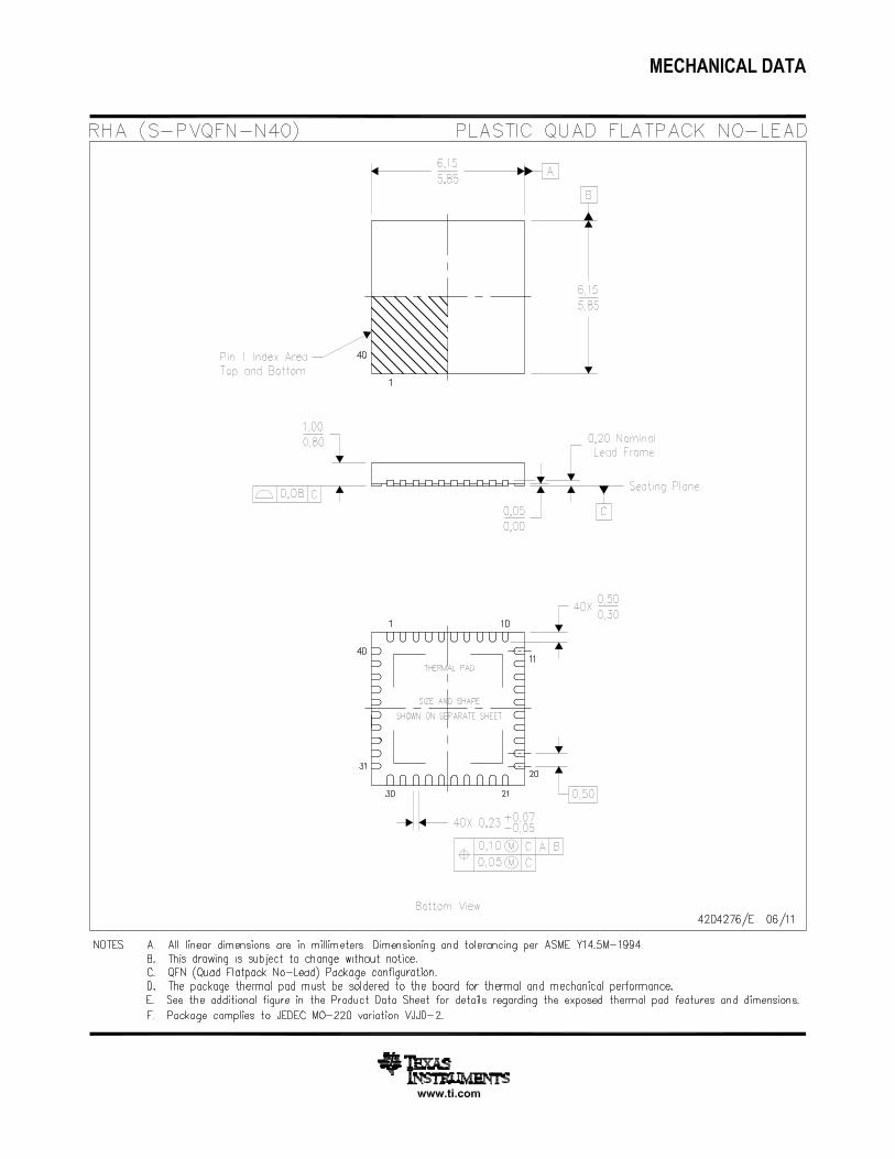
Asynchronous Networks – AES Security Coprocessor– Space-Saving 6-mm × 6-mm QFN40 – Two Powerful USARTs With Support for
Package UART and SPI– Suitable for Systems Targeting Compliance – I2C Interface
With Worldwide Radio-Frequency– 23 General-Purpose I/O PinsRegulations: ETSI EN 300 328 and EN 300– Watchdog Timer440 (Europe), FCC CFR47 Part 15 (US), and
ARIB STD-T-66 (Japan) • Development Tools– Pin- and Software-Compatible With the – CC2533 Remote Control Development Kit
CC2530Fxxx Series for RF4CE• Low Power – CC2533 Development Kit
– Active-Mode RX (CPU Idle): 25 mA – CC2533EMK Evaluation Modules– Active Mode TX at 0 dBm (CPU Idle): – SmartRF™ Software
28.5 mA – Packet Sniffer– Power Mode 1 (4 ms Wake-Up): 0.2 mA – IAR Embedded Workbench™ Available– Power Mode 2 (Sleep Timer Running): 1 mA
APPLICATIONS– Power Mode 3 (External Interrupts): 0.5 mA• ZigBee™ RF4CE Remote Control Target and– Wide Supply-Voltage Range (2 V–3.6 V)
Device• Microcontroller
• 2.4-GHz IEEE 802.15.4 Systems Based on– High-Performance and Low-Power 8051 TIMAC or SimpliciTI™ Network Protocol
Microcontroller Core With Code Prefetch • Consumer Electronics– 64- or 96-KB In-System-Programmable • Electronic Shelf Labeling
Flash– 4- or 6-KB RAM With Retention in All Power
Modes– Hardware Debug Support
1
Please be aware that an important notice concerning availability, standard warranty, and use in critical applications of TexasInstruments semiconductor products and disclaimers thereto appears at the end of this data sheet.
2SmartRF, SimpliciTI, RemoTI are trademarks of Texas Instruments.3IAR Embedded Workbench is a trademark of IAR Systems AB.4ZigBee is a trademark of ZigBee Alliance.
DESCRIPTIONThe CC2533 is an optimized system-on-chip (SoC) solution for IEEE 802.15.4 based remote-control systems. Itenables single-chip remote controls to be built with low bill-of-material cost when used as a flexible SoC. It alsoprovides a simple path to adding RF4CE capability to a device or target when used in the wireless networkprocessor configuration of the RemoTI™ RF4CE stack. Robust network nodes can be built with very low totalbill-of-material costs.
The CC2533 combines the excellent performance of a leading RF transceiver with a single-cycle 8051 compliantCPU, up to 96-KB in-system programmable flash memory, up to 6-KB RAM, and many other powerful features.The CC2533 has efficient power modes with RAM and register retention below 1 µA, making it highly suited forlow-duty-cycle systems where ultralow power consumption is required. Short transition times between operatingmodes further ensure low energy consumption.
Combined with the golden-unit-status RemoTI stack from Texas Instruments, the CC2533 provides a robust andcomplete ZigBee RF4CE remote-control solution. It is also ideal for implementing the target side of aremote-control system in a network processor configuration with an SPI/UART/I2C interface. The CC2533 comescomplete with reference designs and example software that implement a remote control system to ensureefficient design-in.
The CC2533 exists in three memory-size configurations:
This integrated circuit can be damaged by ESD. Texas Instruments recommends that all integrated circuits be handled withappropriate precautions. Failure to observe proper handling and installation procedures can cause damage.
ESD damage can range from subtle performance degradation to complete device failure. Precision integrated circuits may be moresusceptible to damage because very small parametric changes could cause the device not to meet its published specifications.
Supply voltage All supply pins must have the same voltage –0.3 3.9 V
–0.3 VDD + 0.3,Voltage on any digital pin V≤ 3.9
Input RF level 10 dBm
Storage temperature range –40 125 °C
All pads, according to human-body model, JEDEC STD 22, method 2 kVA114
ESD (2) According to charged-device model, JEDEC STD 22, method C101 500 V
All pads excluding RF pads, according to machine model, JEDEC STD 200 V22, method A115
(1) Stresses beyond those listed under Absolute Maximum Ratings may cause permanent damage to the device. These are stress ratingsonly, and functional operation of the device at these or any other conditions beyond those indicated under Recommended OperatingConditions is not implied. Exposure to absolute-maximum-rated conditions for extended periods may affect device reliability.
(2) CAUTION: ESD-sensitive device. Precautions should be used when handling the device in order to prevent permanent damage.
RECOMMENDED OPERATING CONDITIONSMIN MAX UNIT
Operating ambient temperature range, TA –40 125 °C
Operating supply voltage 2 3.6 V
ELECTRICAL CHARACTERISTICSMeasured on Texas Instruments CC2533 EM reference design with TA = 25°C and VDD = 3 V, unless otherwise noted.Boldface limits apply over the entire operating range, TA = –40°C to 125°C, VDD = 2 V to 3.6 V, and fc = 2394 MHz to2507 MHz.
PARAMETER TEST CONDITIONS MIN TYP MAX UNIT
Digital regulator on. 16-MHz RCOSC running. No radio,crystals, or peripherals active. 3.6 mAMedium CPU activity: normal flash access (1), no RAM access
32-MHz XOSC running. No radio or peripherals active.6.6 7.7 mA
Medium CPU activity: normal flash access (1), no RAM access
32-MHz XOSC running, radio in RX mode, –50-dBm input 21.6 mApower, no peripherals active, CPU idle
32-MHz XOSC running, radio in RX mode at –100-dBm input 25.1 29.8 mApower (waiting for signal), no peripherals active, CPU idle
32-MHz XOSC running, radio in TX mode, 0-dBm output 28.5 mApower, no peripherals active, CPU idle
32-MHz XOSC running, radio in TX mode, 4.5-dBm outputIcore Core current consumption 32.3 40.6 mApower, no peripherals active, CPU idle
32-MHz XOSC running, radio in boost mode TX, 7-dBm output 38.8 mApower, no peripherals active, CPU idle
Power mode 1. Digital regulator on; 16-MHz RCOSC and32-MHz crystal oscillator off; 32.768-kHz XOSC, POR, BOD, 0.2 0.3 mAand sleep timer active; RAM and register retention
Power mode 2. Digital regulator off; 16-MHz RCOSC and32-MHz crystal oscillator off; 32.768-kHz XOSC, POR, and 1 1.5 mAsleep timer active; RAM and register retention
Power mode 3. Digital regulator off; no clocks; POR active; 0.4 0.7 mARAM and register retention
During reset with supply voltage of 1.2 V 54 mA
(1) Normal flash access means that the code used exceeds the cache storage, so cache misses happen frequently.
ELECTRICAL CHARACTERISTICS (continued)Measured on Texas Instruments CC2533 EM reference design with TA = 25°C and VDD = 3 V, unless otherwise noted.Boldface limits apply over the entire operating range, TA = –40°C to 125°C, VDD = 2 V to 3.6 V, and fc = 2394 MHz to2507 MHz.
PARAMETER TEST CONDITIONS MIN TYP MAX UNIT
Peripheral Current Consumption (Adds to core current Icore for each peripheral unit activated)
Timer 1 Timer running, 32-MHz XOSC used 90 mA
Timer 2 Timer running, 32-MHz XOSC used 90 mA
Timer 3 Timer running, 32-MHz XOSC used 60 mA
Iperi Timer 4 Timer running, 32-MHz XOSC used 70 mA
Sleep timer Including 32.753-kHz RCOSC 0.6 mA
Battery monitor When comparing 93 mA
Erase 0.2 mAFlash
Burst-write peak current 6 mA
GENERAL CHARACTERISTICSMeasured on Texas Instruments CC2533 EM reference design with TA = 25°C and VDD = 3 V, unless otherwise noted.
PARAMETER TEST CONDITIONS MIN TYP MAX UNIT
WAKE-UP AND TIMING
Digital regulator on, 16-MHz RCOSC and 32-MHz crystalPower mode 1 → active 4 msoscillator off. Start-up of 16-MHz RCOSC
Digital regulator off, 16-MHz RCOSC and 32-MHz crystalPower mode 2 or 3 → active 0.1 msoscillator off. Start-up of regulator and 16-MHz RCOSC
Initially running on 16-MHz RCOSC, with 32-MHz XOSC 0.6 msOFFActive → TX or RXWith 32-MHz XOSC initially on 192 ms
RX/TX and TX/RX turnaround 192 ms
RADIO PART
Programmable in 1-MHz steps, 5 MHz between channelsRF frequency range 2394 2507 MHzfor compliance with [1]
RF RECEIVE SECTIONMeasured on Texas Instruments CC2533 EM reference design with TA = 25°C, VDD = 3 V, and fc = 2440 MHz, unlessotherwise noted.Boldface limits apply over the entire operating range, TA = –40°C to 125°C, VDD = 2 V to 3.6 V, and fc = 2394 MHz to2507 MHz.
PARAMETER TEST CONDITIONS MIN TYP MAX UNIT
PER = 1%, as specified by [1] –97 –93Receiver sensitivity dBm–89[1] requires –85 dBm
PER = 1%, as specified by [1]Saturation (maximum input level) 10 dBm
[1] requires –20 dBm
Wanted signal –82 dBm, adjacent modulated channel atAdjacent-channel rejection, 5-MHz 5 MHz, PER = 1%, as specified by [1]. 49 dBchannel spacing
[1] requires 0 dB
Wanted signal –82 dBm, adjacent modulated channel atAdjacent-channel rejection, –5-MHz –5 MHz, PER = 1%, as specified by [1]. 49 dBchannel spacing
[1] requires 0 dB
Wanted signal –82 dBm, adjacent modulated channel atAlternate-channel rejection, 10-MHz 10 MHz, PER = 1%, as specified by [1] 57 dBchannel spacing
[1] requires 30 dB
Wanted signal –82 dBm, adjacent modulated channel atAlternate-channel rejection, –10-MHz –10 MHz, PER = 1%, as specified by [1] 57 dBchannel spacing
[1] requires 30 dB
Channel rejection Wanted signal at –82 dBm. Undesired signal is an IEEE≥ 20 MHz 802.15.4 modulated channel, stepped through all channels 57 dB
from 2405 to 2480 MHz. Signal level for PER = 1%.≤ –20 MHz 57
Wanted signal at –82 dBm. Undesired signal is 802.15.4Co-channel rejection modulated at the same frequency as the desired signal. Signal –2 dB
level for PER = 1%.
Blocking/desensitization
Measured according to ETSI EN 300 440-1 V1.6.1 (2010-04)–250 MHz from band edge -37blocking/desensitization. Wanted signal 3 dB above sensitivity
–100 MHz from band edge -35limit, interferer at 10×, 20× and 50× bandwidth from receiverdBm–50 MHz from band edge channel band edge. Limit > –45dBm for class-2 receiver. -40
50 MHz from band edge -38
100 MHz from band edge -33
250 MHz from band edge -32
Spurious emission. Only largest spuriousemission stated within each band. Conducted measurement with a 50-Ω single-ended load.
Suitable for systems targeting compliance with EN 300 328, dBm30 MHz–1000 MHz <EN 300 440, FCC CFR47 Part 15, and ARIB STD-T-66. –801 GHz–12.75 GHz
(1) Difference between center frequency of the received RF signal and local oscillator frequency.(2) Difference between incoming symbol rate and the internally generated symbol rate
RF TRANSMIT SECTIONMeasured on Texas Instruments CC2533 EM reference design with TA = 25°C, VDD = 3 V and fc = 2440 MHz, unlessotherwise noted.Boldface limits apply over the entire operating range, TA = –40°C to 125°C, VDD = 2 V to 3.6 V, and fc = 2394 MHz to 2507MHz.
PARAMETER TEST CONDITIONS MIN TYP MAX UNIT
Delivered to a single-ended 50-Ω load through a balun using 4.51 4.5 7dBm output-power settingNominal output power dBm–3 8
[1] requires minimum –3 dBm
Delivered to a single-ended 50-Ω load through a balun using boostBoost mode 7 dBmmode TX settings
Programmable output-power 27 dBrange
Spurious emissions 4.5 dBm output power setting (1)
25 MHz–1000 MHz (outside restricted bands) (2) (2) –6025 MHz–2400 MHz (within FCC restricted bands) (2) –6025 MHz–1000 MHz (within ETSI restricted bands) (2) –601800–1900 MHz (ETSI restricted band) (2) –565150–5300 MHz (ETSI restricted band) (2) –54 dBmAt 2 × fc and 3 × fc (FCC restricted band) (2) –48At 2 × fc and 3 × fc (ETSI EN 300-440 and EN 300-328) (3) (2) –391 GHz–12.75 GHz (outside restricted bands) (2) –60At 2483.5 MHz and above (FCC restricted band) (2)
fc= 2480 MHz (4) (2)–45
Measured as defined by [1] using 4.5 dBm output-power settingError vector magnitude (EVM) 3%
[1] requires maximum 35%.
Differential impedance as seen from the RF port (RF_P and RF_N)Optimum load impedance 69 + j29 Ωtowards the antenna
(1) Texas Instruments CC2533 EM reference design is suitable for systems targeting compliance with EN 300 328, EN 300 440, FCCCFR47 Part 15, and ARIB STD-T-66.
(2) Measurement conducted according to stated regulations. Only largest spurious emission stated within each band.(3) Margins for passing conducted requirements at the third harmonic can be improved by using a simple band-pass filter connected
between matching network and RF connector (1.8 pF in parallel with 1.6 nH); this filter must be connected to a good RF ground.(4) Margins for passing FCC requirements at 2483.5 MHz and above when transmitting at 2480 MHz can be improved by using a lower
output-power setting or having less than 100% duty cycle.
(1) Including aging and temperature dependency, as specified by [1]
32-kHz RC OSCILLATORMeasured on Texas Instruments CC2533 EM reference design with TA = 25°C and VDD = 3 V, unless otherwise noted.
PARAMETER TEST CONDITIONS MIN TYP MAX UNIT
Calibrated frequency (1) 32.753 kHz
Frequency accuracy after calibration ±0.2%
Temperature coefficient (2) 0.4 %/°C
Supply-voltage coefficient (3) 3 %/V
Calibration time (4) 2 ms
(1) The calibrated 32-kHz RC oscillator frequency is the 32-MHz XTAL frequency divided by 977.(2) Frequency drift when temperature changes after calibration(3) Frequency drift when supply voltage changes after calibration(4) When the 32-kHz RC oscillator is enabled, it is calibrated when a switch from the 16-MHz RC oscillator to the 32-MHz crystal oscillator
16-MHz RC OSCILLATORMeasured on Texas Instruments CC2533 EM reference design with TA = 25°C and VDD = 3 V
PARAMETER TEST CONDITIONS MIN TYP MAX UNIT
Frequency (1) 16 MHz
Uncalibrated frequency accuracy ±18%
Calibrated frequency accuracy ±0.6% ±1%
Start-up time 10 ms
Initial calibration time (2) 50 ms
(1) The calibrated 16-MHz RC oscillator frequency is the 32-MHz XTAL frequency divided by 2.(2) When the 16-MHz RC oscillator is enabled, it is calibrated when a switch from the 16-MHz RC oscillator to the 32-MHz crystal oscillator
is performed while SLEEPCMD.OSC_PD is set to 0.
RSSI/CCA CHARACTERISTICSMeasured on Texas Instruments CC2533 EM reference design with TA = 25°C and VDD = 3 V
PARAMETER TEST CONDITIONS MIN TYP MAX UNIT
RSSI range 100 dB
Absolute uncalibrated RSSI/CCA accuracy ±4 dB
RSSI/CCA offset 73 dB
Step size (LSB value) 1 dB
FREQEST CHARACTERISTICSMeasured on Texas Instruments CC2533 EM reference design with TA = 25°C and VDD = 3 V
PARAMETER TEST CONDITIONS MIN TYP MAX UNIT
FREQEST range ±250 kHz
FREQEST accuracy ±40 kHz
FREQEST offset 20 kHz
Step size (LSB value) 7.8 kHz
FREQUENCY SYNTHESIZER CHARACTERISTICSMeasured on Texas Instruments CC2533 EM reference design with TA = 25°C, VDD = 3 V, and fc = 2440 MHz
PARAMETER TEST CONDITIONS MIN TYP MAX UNIT
At ±1-MHz offset from carrier –110
Phase noise, unmodulated carrier At ±2-MHz offset from carrier –117 dBc/Hz
At ±5-MHz offset from carrier –122
BATTERY MONITOR CHARACTERISTICSMeasured on Texas Instruments CC2533 EM reference design with TA = 25°C and VDD = 3 V
PARAMETER TEST CONDITIONS MIN TYP MAX UNIT
Settling time 2 µs
For voltages up to 2.5 V 24 mVStep size
For voltages above 2.5 V 169 mV
Across 1.95 V to 2.5 V, with single-point calibration at 1.95 V 2 20 mVCalibrated accuracy
Across 2.5 V to 3.6 V, with single-point calibration at 1.95 V 10 55 mV
CONTROL INPUT AC CHARACTERISTICSTA = –40°C to 125°C, VDD = 2 V to 3.6 V
PARAMETER TEST CONDITIONS MIN TYP MAX UNIT
System clock, fSYSCLK The undivided system clock is 32 MHz when crystal oscillator is used.The undivided system clock is 16 MHz when calibrated 16-MHz RC 16 32 MHztSYSCLK = 1/fSYSCLKoscillator is used.
CONTROL INPUT AC CHARACTERISTICS (continued)TA = –40°C to 125°C, VDD = 2 V to 3.6 V
PARAMETER TEST CONDITIONS MIN TYP MAX UNIT
See item 1, Figure 1. This is the shortest pulse that is recognized asa complete reset-pin request. Note that shorter pulses may beRESET_N low duration 1 msrecognized but might not lead to complete reset of all modules withinthe chip.
See item 2, Figure 1.This is the shortest pulse that is recognized asInterrupt pulse duration 20 nsan interrupt request.
TIMER INPUT AC CHARACTERISTICSTA = –40°C to 125°C, VDD = 2 V to 3.6 V
PARAMETER TEST CONDITIONS MIN TYP MAX UNIT
Synchronizers determine the shortest input pulse that can be recognized. tSYSCLKInput capture pulse duration The synchronizers operate at the current system clock rate (16 MHz or 32 1.5
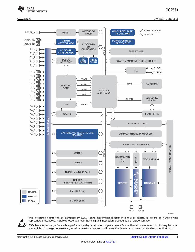
A block diagram of the CC2533 is shown in Figure 8. The modules can be roughly divided into one of threecategories: CPU- and memory-related modules; modules related to peripherals, clocks, and power management;and radio-related modules. In the following subsections, a short description of each module that appears inFigure 8 is given.
For more details about the modules and their usage, see the corresponding chapters in the CC253x User'sGuide (SWRU191).
CPU and Memory
The 8051 CPU core used in the CC253x device family is a single-cycle 8051-compatible core. It has threedifferent memory-access buses (SFR, DATA, and CODE/XDATA) with single-cycle access to SFR, DATA, andthe main SRAM. It also includes a debug interface and an 18-input extended interrupt unit.
The interrupt controller services a total of 18 interrupt sources, divided into six interrupt groups, each of whichis associated with one of four interrupt priorities. Any interrupt service request is serviced also when the device isin idle mode by going back to active mode. Some interrupts can also wake up the device from sleep mode(power modes 1–3).
The memory arbiter is at the heart of the system, as it connects the CPU and DMA controller with the physicalmemories and all peripherals through the SFR bus. The memory arbiter has four memory access points, accessof which can map to one of three physical memories: an 8-KB SRAM, flash memory, and XREG/SFR registers. Itis responsible for performing arbitration and sequencing between simultaneous memory accesses to the samephysical memory.
The 4- or 6-KB SRAM maps to the DATA memory space and to parts of the XDATA memory spaces. The 6-KBSRAM is an ultralow-power SRAM that retains its contents even in the lowest power modes (PM2/3). This is animportant feature for low-power applications.
The 64- or 96-KB flash block provides in-circuit programmable non-volatile program memory for the device, andmaps into the CODE and XDATA memory spaces. In addition to holding program code and constants, thenon-volatile memory allows the application to save data that must be preserved such that it is available afterrestarting the device. Using this feature, one can, e.g., use saved network-specific data to avoid the need for afull start-up and network find-and-join process.
Clocks and Power Management
The digital core and peripherals are powered by a 1.8-V low-dropout voltage regulator. It provides powermanagement functionality that enables low-power operation for long battery life using different power modes.Five different reset sources exist to reset the device.
Peripherals
The CC2533 includes many different peripherals that allow the application designer to develop advancedapplications.
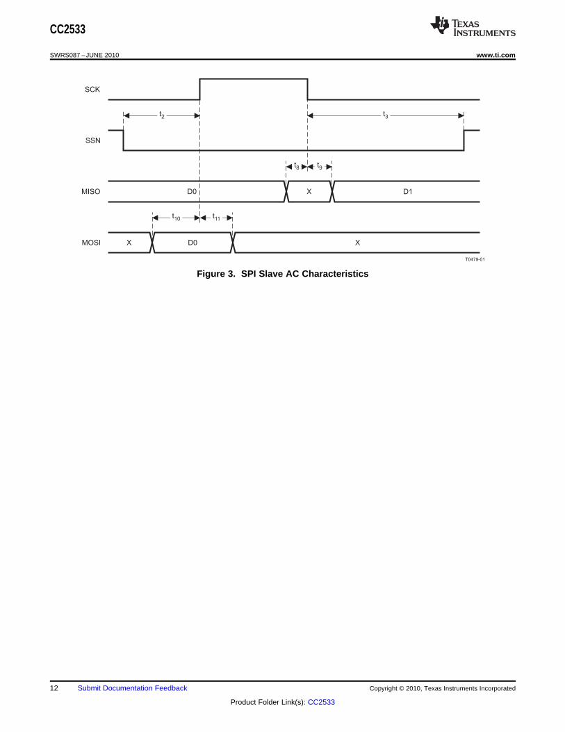
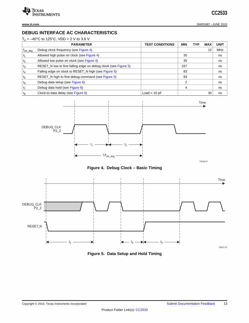
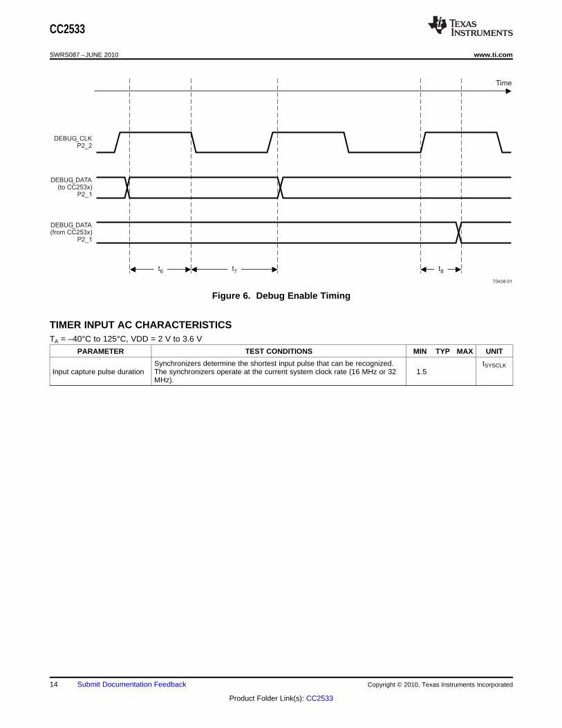
The debug interface implements a proprietary two-wire serial interface that is used for in-circuit debugging.Through this debug interface, it is possible to perform an erasure of the entire flash memory, control whichoscillators are enabled, stop and start execution of the user program, execute supplied instructions on the 8051core, set code breakpoints, and single-step through instructions in the code. Using these techniques, it ispossible to perform in-circuit debugging and external flash programming elegantly.
The device contains flash memory for storage of program code. The flash memory is programmable from theuser software and through the debug interface. The flash controller handles writing and erasing the embeddedflash memory. The flash controller allows page-wise erasure and 4-bytewise programming.
The I/O controller is responsible for all general-purpose I/O pins. The CPU can configure whether peripheralmodules control certain pins or whether they are under software control, and if so, whether each pin is configuredas an input or output and if a pullup or pulldown resistor in the pad is connected. CPU interrupts can be enabledon each pin individually. Each peripheral that connects to the I/O pins can choose between two different I/O pinlocations to ensure flexibility in various applications.
A versatile five-channel DMA controller is available in the system, accesses memory using the XDATA memoryspace, and thus has access to all physical memories. Each channel (trigger, priority, transfer mode, addressingmode, source and destination pointers, and transfer count) is configured with DMA descriptors anywhere inmemory. Many of the hardware peripherals (AES core, flash controller, USARTs, timers, ADC interface) achievehighly efficient operation by using the DMA controller for data transfers between SFR or XREG addresses andflash/SRAM.
Timer 1 is a 16-bit timer with timer/counter/PWM functionality. It has a programmable prescaler, a 16-bit periodvalue, and five individually programmable counter/capture channels, each with a 16-bit compare value. Each ofthe counter/capture channels can be used as a PWM output or to capture the timing of edges on input signals. Itcan also be configured in IR Generation Mode, where it counts Timer 3 periods and the output is ANDed withthe output of Timer 3 to generate modulated consumer IR signals with minimal CPU interaction.
Timer 2 (the MAC Timer) is specially designed for supporting an IEEE 802.15.4 MAC or other time-slottedprotocol in software. The timer has a configurable timer period and a 24-bit overflow counter that can be used tokeep track of the number of periods that have transpired. A 40-bit capture register is also used to record theexact time at which a start-of-frame delimiter is received/transmitted or the exact time at which transmissionends, as well as two 16-bit output compare registers and two 24-bit overflow compare registers that can sendvarious command strobes (start RX, start TX, etc.) at specific times to the radio modules.
Timer 3 and Timer 4 are 8-bit timers with timer/counter/PWM functionality. They have a programmableprescaler, an 8-bit period value, and one programmable counter channel with an 8-bit compare value. Each ofthe counter channels can be used as a PWM output.
The sleep timer is an ultralow-power timer that counts 32-kHz crystal oscillator or 32-kHz RC oscillator periods.The sleep timer runs continuously in all operating modes except power mode 3 (PM3). Typical applications ofthis timer are as a real-time counter or as a wake-up timer to come out of power mode 1 (PM1) or 2 (PM2).
The battery monitor comparator enables simple voltage monitoring in the devices that do not include an ADC. Itis designed such that it is accurate in the voltage areas around 2 V, with lower resolution at higher voltages.
The random-number generator uses a 16-bit LFSR to generate pseudorandom numbers, which can be read bythe CPU or used directly by the command strobe processor. It can be seeded with random data from noise in theradio ADC.
The AES encryption/decryption core allows the user to encrypt and decrypt data using the AES algorithm with128-bit keys. The core is able to support the security operations required by IEEE 802.15.4 MAC security, theZigBee network layer, and the application layer.
A built-in watchdog timer allows the CC2533 to reset itself in case the firmware hangs. When enabled bysoftware, the watchdog timer must be cleared periodically; otherwise, it resets the device when it times out. It canalternatively be configured for use as a general 32-kHz timer.
USART 0 and USART 1 are each configurable as either a SPI master/slave or a UART. They provide doublebuffering on both RX and TX, as well as hardware flow control, and are thus well suited to high-throughputfull-duplex applications. Each has its own high-precision baud-rate generator, thus leaving the ordinary timersfree for other uses.
The I2C module provides a digital peripheral connection with two pins and supports both master and slaveoperation.
Radio
The CC2533 features an IEEE 802.15.4-compliant radio transceiver. The RF core controls the analog radiomodules. In addition, it provides an interface between the MCU and the radio which makes it possible to issuecommands, read status, and automate and sequence radio events. The radio also includes a packet-filtering andaddress-recognition module.
This section contains a summary of the register settings that must be updated from their default value to haveoptimal performance. The following settings should be set for both RX and TX. Although not all settings arenecessary for both RX and TX, it is recommended for simplicity (allowing one set of settings to be written at theinitialization of the code).
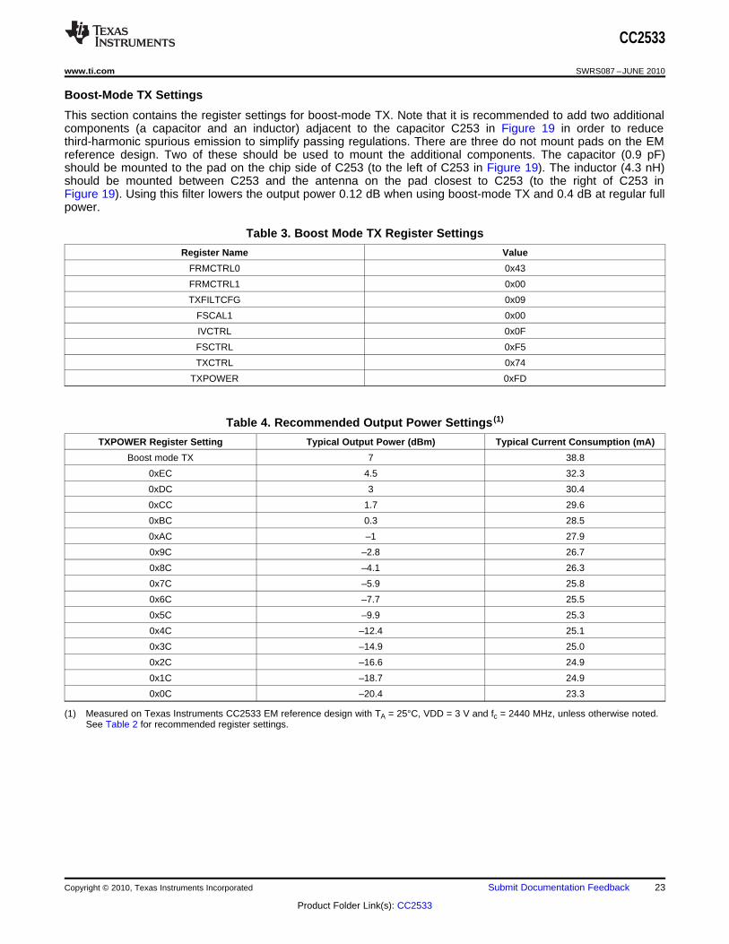
This section contains the register settings for boost-mode TX. Note that it is recommended to add two additionalcomponents (a capacitor and an inductor) adjacent to the capacitor C253 in Figure 19 in order to reducethird-harmonic spurious emission to simplify passing regulations. There are three do not mount pads on the EMreference design. Two of these should be used to mount the additional components. The capacitor (0.9 pF)should be mounted to the pad on the chip side of C253 (to the left of C253 in Figure 19). The inductor (4.3 nH)should be mounted between C253 and the antenna on the pad closest to C253 (to the right of C253 inFigure 19). Using this filter lowers the output power 0.12 dB when using boost-mode TX and 0.4 dB at regular fullpower.
Table 3. Boost Mode TX Register Settings
Register Name Value
FRMCTRL0 0x43
FRMCTRL1 0x00
TXFILTCFG 0x09
FSCAL1 0x00
IVCTRL 0x0F
FSCTRL 0xF5
TXCTRL 0x74
TXPOWER 0xFD
Table 4. Recommended Output Power Settings (1)
TXPOWER Register Setting Typical Output Power (dBm) Typical Current Consumption (mA)
Boost mode TX 7 38.8
0xEC 4.5 32.3
0xDC 3 30.4
0xCC 1.7 29.6
0xBC 0.3 28.5
0xAC –1 27.9
0x9C –2.8 26.7
0x8C –4.1 26.3
0x7C –5.9 25.8
0x6C –7.7 25.5
0x5C –9.9 25.3
0x4C –12.4 25.1
0x3C –14.9 25.0
0x2C –16.6 24.9
0x1C –18.7 24.9
0x0C –20.4 23.3
(1) Measured on Texas Instruments CC2533 EM reference design with TA = 25°C, VDD = 3 V and fc = 2440 MHz, unless otherwise noted.See Table 2 for recommended register settings.
Power-Supply Decoupling Capacitors Are Not ShownDigital I/O Not Connected
Antenna
(50 )W
S0383-02
L251
CC2533
SWRS087 –JUNE 2010 www.ti.com
APPLICATION INFORMATION
Few external components are required for the operation of the CC2533. A typical application circuit is shown inFigure 19. Typical values and description of external components are shown in Table 5.
Figure 19. CC2533 Application Circuit
Table 5. Overview of External Components (Excluding Supply DecouplingCapacitors)
Component Description Value
C221 32-MHz xtal loading capacitor 27 pF
C231 32-MHz xtal loading capacitor 27 pF
C251 Part of the RF matching network 18 pF
C252 Part of the RF matching network 1 pF
C253 Part of the RF matching network 2.2 pF
C261 Part of the RF matching network 18 pF
C262 Part of the RF matching network 1 pF
C321 32-kHz xtal loading capacitor 15 pF
C331 32-kHz xtal loading capacitor 15 pF
C401 Decoupling capacitor for the internal digital regulator 1 mF
Table 5. Overview of External Components (Excluding Supply DecouplingCapacitors) (continued)
Component Description Value
L261 Part of the RF matching network 2 nH
R301 Resistor used for internal biasing 56 kΩ
Input/Output Matching
When using an unbalanced antenna such as a monopole, a balun should be used to optimize performance. Thebalun can be implemented using low-cost discrete inductors and capacitors. The recommended balun shownconsists of C262, L261, C252, and L252.
If a balanced antenna such as a folded dipole is used, the balun can be omitted.
Crystal
An external 32-MHz crystal, XTAL1, with two loading capacitors (C221 and C231) is used for the 32-MHz crystaloscillator. See the 32-MHz Crystal Oscillator section for details. The load capacitance seen by the 32-MHzcrystal is given by:
(1)
XTAL2 is an optional 32.768-kHz crystal, with two loading capacitors (C321 and C331) used for the 32.768-kHzcrystal oscillator. The 32.768-kHz crystal oscillator is used in applications where both very low sleep-currentconsumption and accurate wake-up times are needed. The load capacitance seen by the 32.768-kHz crystal isgiven by:
(2)
A series resistor may be used to comply with the ESR requirement.
On-Chip 1.8-V Voltage-Regulator Decoupling
The 1.8-V on-chip voltage regulator supplies the 1.8-V digital logic. This regulator requires a decoupling capacitor(C401) for stable operation.
Power-Supply Decoupling and Filtering
Proper power-supply decoupling must be used for optimum performance. The placement and size of thedecoupling capacitors and the power supply filtering are very important to achieve the best performance in anapplication. TI provides a compact reference design that should be followed very closely.
REFERENCES1. IEEE Std. 802.15.4-2006: Wireless Medium Access Control (MAC) and Physical Layer (PHY) Specifications
for Low-Rate Wireless Personal Area Networks (LR-WPANs)http://standards.ieee.org/getieee802/download/802.15.4-2006.pdf
2. CC253x User's Guide – CC253x System-on-Chip Solution for 2.4 GHz IEEE 802.15.4 and ZigBeeApplications (SWRU191)
Texas Instruments offers a wide selection of cost-effective, low-power RF solutions for proprietary andstandard-based wireless applications for use in industrial and consumer applications. Our selection includes RFtransceivers, RF transmitters, RF front ends, and System-on-Chips as well as various software solutions for thesub-1-GHz and 2.4-GHz frequency bands.
In addition, Texas Instruments provides a large selection of support collateral such as development tools,technical documentation, reference designs, application expertise, customer support, third-party and universityprograms.
The Low-Power RF E2E Online Community provides technical support forums, videos and blogs, and the chanceto interact with fellow engineers from all over the world.
With a broad selection of product solutions, end application possibilities, and a range of technical support, TexasInstruments offers the broadest low-power RF portfolio. We make RF easy!
The following subsections point to where to find more information.
Texas Instruments Low-Power RF Web Site
Texas Instruments’ Low-Power RF Web site has all our latest products, application and design notes, FAQsection, news and events updates, and much more. Just go to www.ti.com/lprf.
Texas Instruments has launched an extensive network of low-power RF development partners to help customersspeed up their application development. The network consists of recommended companies, RF consultants, andindependent design houses that provide a series of hardware module products and design services, including:• RF circuit, low-power RF, and ZigBee design services• Low-power RF and ZigBee module solutions and development tools• RF certification services and RF circuit manufacturing
Need help with modules, engineering services or development tools?
Search the Low-Power RF Developer Network to find a suitable partner. www.ti.com/lprfnetwork
Low-Power RF eNewsletter
The Low-Power RF eNewsletter keeps you up-to-date on new products, news releases, developers’ news, andother news and events associated with low-power RF products from TI. The Low-Power RF eNewsletter articlesinclude links to get more online information.
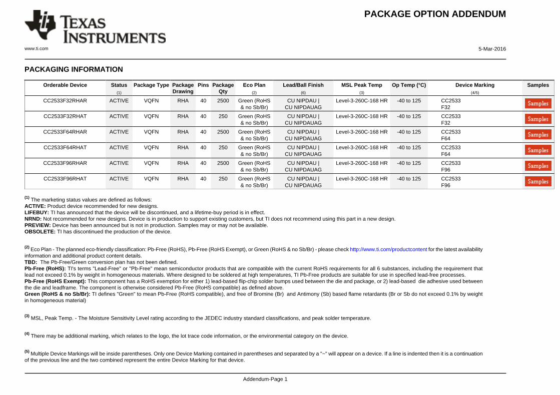
CC2533F32RHAR ACTIVE VQFN RHA 40 2500 Green (RoHS& no Sb/Br)
CU NIPDAU |CU NIPDAUAG
Level-3-260C-168 HR -40 to 125 CC2533F32
CC2533F32RHAT ACTIVE VQFN RHA 40 250 Green (RoHS& no Sb/Br)
CU NIPDAU |CU NIPDAUAG
Level-3-260C-168 HR -40 to 125 CC2533F32
CC2533F64RHAR ACTIVE VQFN RHA 40 2500 Green (RoHS& no Sb/Br)
CU NIPDAU |CU NIPDAUAG
Level-3-260C-168 HR -40 to 125 CC2533F64
CC2533F64RHAT ACTIVE VQFN RHA 40 250 Green (RoHS& no Sb/Br)
CU NIPDAU |CU NIPDAUAG
Level-3-260C-168 HR -40 to 125 CC2533F64
CC2533F96RHAR ACTIVE VQFN RHA 40 2500 Green (RoHS& no Sb/Br)
CU NIPDAU |CU NIPDAUAG
Level-3-260C-168 HR -40 to 125 CC2533F96
CC2533F96RHAT ACTIVE VQFN RHA 40 250 Green (RoHS& no Sb/Br)
CU NIPDAU |CU NIPDAUAG
Level-3-260C-168 HR -40 to 125 CC2533F96
(1) The marketing status values are defined as follows:ACTIVE: Product device recommended for new designs.LIFEBUY: TI has announced that the device will be discontinued, and a lifetime-buy period is in effect.NRND: Not recommended for new designs. Device is in production to support existing customers, but TI does not recommend using this part in a new design.PREVIEW: Device has been announced but is not in production. Samples may or may not be available.OBSOLETE: TI has discontinued the production of the device.
(2) Eco Plan - The planned eco-friendly classification: Pb-Free (RoHS), Pb-Free (RoHS Exempt), or Green (RoHS & no Sb/Br) - please check http://www.ti.com/productcontent for the latest availabilityinformation and additional product content details.TBD: The Pb-Free/Green conversion plan has not been defined.Pb-Free (RoHS): TI's terms "Lead-Free" or "Pb-Free" mean semiconductor products that are compatible with the current RoHS requirements for all 6 substances, including the requirement thatlead not exceed 0.1% by weight in homogeneous materials. Where designed to be soldered at high temperatures, TI Pb-Free products are suitable for use in specified lead-free processes.Pb-Free (RoHS Exempt): This component has a RoHS exemption for either 1) lead-based flip-chip solder bumps used between the die and package, or 2) lead-based die adhesive used betweenthe die and leadframe. The component is otherwise considered Pb-Free (RoHS compatible) as defined above.Green (RoHS & no Sb/Br): TI defines "Green" to mean Pb-Free (RoHS compatible), and free of Bromine (Br) and Antimony (Sb) based flame retardants (Br or Sb do not exceed 0.1% by weightin homogeneous material)
(3) MSL, Peak Temp. - The Moisture Sensitivity Level rating according to the JEDEC industry standard classifications, and peak solder temperature.
(4) There may be additional marking, which relates to the logo, the lot trace code information, or the environmental category on the device.
(5) Multiple Device Markings will be inside parentheses. Only one Device Marking contained in parentheses and separated by a "~" will appear on a device. If a line is indented then it is a continuationof the previous line and the two combined represent the entire Device Marking for that device.
(6) Lead/Ball Finish - Orderable Devices may have multiple material finish options. Finish options are separated by a vertical ruled line. Lead/Ball Finish values may wrap to two lines if the finishvalue exceeds the maximum column width.
Important Information and Disclaimer:The information provided on this page represents TI's knowledge and belief as of the date that it is provided. TI bases its knowledge and belief on informationprovided by third parties, and makes no representation or warranty as to the accuracy of such information. Efforts are underway to better integrate information from third parties. TI has taken andcontinues to take reasonable steps to provide representative and accurate information but may not have conducted destructive testing or chemical analysis on incoming materials and chemicals.TI and TI suppliers consider certain information to be proprietary, and thus CAS numbers and other limited information may not be available for release.
In no event shall TI's liability arising out of such information exceed the total purchase price of the TI part(s) at issue in this document sold by TI to Customer on an annual basis.
Texas Instruments Incorporated (TI) reserves the right to make corrections, enhancements, improvements and other changes to itssemiconductor products and services per JESD46, latest issue, and to discontinue any product or service per JESD48, latest issue. Buyersshould obtain the latest relevant information before placing orders and should verify that such information is current and complete.TI’s published terms of sale for semiconductor products (http://www.ti.com/sc/docs/stdterms.htm) apply to the sale of packaged integratedcircuit products that TI has qualified and released to market. Additional terms may apply to the use or sale of other types of TI products andservices.Reproduction of significant portions of TI information in TI data sheets is permissible only if reproduction is without alteration and isaccompanied by all associated warranties, conditions, limitations, and notices. TI is not responsible or liable for such reproduceddocumentation. Information of third parties may be subject to additional restrictions. Resale of TI products or services with statementsdifferent from or beyond the parameters stated by TI for that product or service voids all express and any implied warranties for theassociated TI product or service and is an unfair and deceptive business practice. TI is not responsible or liable for any such statements.Buyers and others who are developing systems that incorporate TI products (collectively, “Designers”) understand and agree that Designersremain responsible for using their independent analysis, evaluation and judgment in designing their applications and that Designers havefull and exclusive responsibility to assure the safety of Designers' applications and compliance of their applications (and of all TI productsused in or for Designers’ applications) with all applicable regulations, laws and other applicable requirements. Designer represents that, withrespect to their applications, Designer has all the necessary expertise to create and implement safeguards that (1) anticipate dangerousconsequences of failures, (2) monitor failures and their consequences, and (3) lessen the likelihood of failures that might cause harm andtake appropriate actions. Designer agrees that prior to using or distributing any applications that include TI products, Designer willthoroughly test such applications and the functionality of such TI products as used in such applications.TI’s provision of technical, application or other design advice, quality characterization, reliability data or other services or information,including, but not limited to, reference designs and materials relating to evaluation modules, (collectively, “TI Resources”) are intended toassist designers who are developing applications that incorporate TI products; by downloading, accessing or using TI Resources in anyway, Designer (individually or, if Designer is acting on behalf of a company, Designer’s company) agrees to use any particular TI Resourcesolely for this purpose and subject to the terms of this Notice.TI’s provision of TI Resources does not expand or otherwise alter TI’s applicable published warranties or warranty disclaimers for TIproducts, and no additional obligations or liabilities arise from TI providing such TI Resources. TI reserves the right to make corrections,enhancements, improvements and other changes to its TI Resources. TI has not conducted any testing other than that specificallydescribed in the published documentation for a particular TI Resource.Designer is authorized to use, copy and modify any individual TI Resource only in connection with the development of applications thatinclude the TI product(s) identified in such TI Resource. NO OTHER LICENSE, EXPRESS OR IMPLIED, BY ESTOPPEL OR OTHERWISETO ANY OTHER TI INTELLECTUAL PROPERTY RIGHT, AND NO LICENSE TO ANY TECHNOLOGY OR INTELLECTUAL PROPERTYRIGHT OF TI OR ANY THIRD PARTY IS GRANTED HEREIN, including but not limited to any patent right, copyright, mask work right, orother intellectual property right relating to any combination, machine, or process in which TI products or services are used. Informationregarding or referencing third-party products or services does not constitute a license to use such products or services, or a warranty orendorsement thereof. Use of TI Resources may require a license from a third party under the patents or other intellectual property of thethird party, or a license from TI under the patents or other intellectual property of TI.TI RESOURCES ARE PROVIDED “AS IS” AND WITH ALL FAULTS. TI DISCLAIMS ALL OTHER WARRANTIES ORREPRESENTATIONS, EXPRESS OR IMPLIED, REGARDING RESOURCES OR USE THEREOF, INCLUDING BUT NOT LIMITED TOACCURACY OR COMPLETENESS, TITLE, ANY EPIDEMIC FAILURE WARRANTY AND ANY IMPLIED WARRANTIES OFMERCHANTABILITY, FITNESS FOR A PARTICULAR PURPOSE, AND NON-INFRINGEMENT OF ANY THIRD PARTY INTELLECTUALPROPERTY RIGHTS. TI SHALL NOT BE LIABLE FOR AND SHALL NOT DEFEND OR INDEMNIFY DESIGNER AGAINST ANY CLAIM,INCLUDING BUT NOT LIMITED TO ANY INFRINGEMENT CLAIM THAT RELATES TO OR IS BASED ON ANY COMBINATION OFPRODUCTS EVEN IF DESCRIBED IN TI RESOURCES OR OTHERWISE. IN NO EVENT SHALL TI BE LIABLE FOR ANY ACTUAL,DIRECT, SPECIAL, COLLATERAL, INDIRECT, PUNITIVE, INCIDENTAL, CONSEQUENTIAL OR EXEMPLARY DAMAGES INCONNECTION WITH OR ARISING OUT OF TI RESOURCES OR USE THEREOF, AND REGARDLESS OF WHETHER TI HAS BEENADVISED OF THE POSSIBILITY OF SUCH DAMAGES.Unless TI has explicitly designated an individual product as meeting the requirements of a particular industry standard (e.g., ISO/TS 16949and ISO 26262), TI is not responsible for any failure to meet such industry standard requirements.Where TI specifically promotes products as facilitating functional safety or as compliant with industry functional safety standards, suchproducts are intended to help enable customers to design and create their own applications that meet applicable functional safety standardsand requirements. Using products in an application does not by itself establish any safety features in the application. Designers mustensure compliance with safety-related requirements and standards applicable to their applications. Designer may not use any TI products inlife-critical medical equipment unless authorized officers of the parties have executed a special contract specifically governing such use.Life-critical medical equipment is medical equipment where failure of such equipment would cause serious bodily injury or death (e.g., lifesupport, pacemakers, defibrillators, heart pumps, neurostimulators, and implantables). Such equipment includes, without limitation, allmedical devices identified by the U.S. Food and Drug Administration as Class III devices and equivalent classifications outside the U.S.TI may expressly designate certain products as completing a particular qualification (e.g., Q100, Military Grade, or Enhanced Product).Designers agree that it has the necessary expertise to select the product with the appropriate qualification designation for their applicationsand that proper product selection is at Designers’ own risk. Designers are solely responsible for compliance with all legal and regulatoryrequirements in connection with such selection.Designer will fully indemnify TI and its representatives against any damages, costs, losses, and/or liabilities arising out of Designer’s non-compliance with the terms and provisions of this Notice.