JOURNAL OF LIGHTWAVE TECHNOLOGY, VOL. 22, NO. 2, FEBRUARY 2004 589
An Optimum Approach for Reduction of FiberAlignment Shift of Fiber-Solder-Ferrule
Joints in Laser Module PackagingWood-Hi Cheng, Senior Member, IEEE, Member, OSA, Maw-Tyan Sheen, Member, IEEE, Chia-Ming Chang,
and Yih-Tun Tseng
Abstract—The results of experimental and numerical inves-tigations leading to an optimum approach for the reduction offiber alignment shift of fiber-solder-ferrule (FSF) joints in lasermodule packaging under temperature cycling test is presented.Using a novel image capture camera system as a monitor probeand the Sn -based solders as bonding materials, we have achievedthe minimum fiber eccentric offsets of 8 and 20 � in FSFjoints with the PbSn and AuSn solders, respectively. After a500-temperature cycling test, the fiber alignment shifts for thesesmall initial fiber eccentric offsets of FSF joints were found to be0.7 and 0.3 � with the PbSn and AuSn solders, respectively. Themeasured fiber shifts were in good agreement with the numericalresults of the finite-element method (FEM) analysis when boththe residual stresses and the creep deformation within the solderwere considered. This study have demonstrated that by solderingthe fiber near to the center of the ferrule, and hence minimizingthe fiber eccentric offset, the fiber alignment shifts of FSF jointsin laser diode module packaging under temperature cycling testcan be reduced significantly.
Index Terms—Fiber-solder-ferrule (FSF) joint, finite-elementmethod (FEM), image capture camera system, laser modulepackaging.
I. INTRODUCTION
THERE are various types of laser diode module packagedesigns. The coaxial and box-type are the most common
styles [1], [2]. The coaxial-type package designs based onTO (transistor outline)-Can are usually selected when thefabrication cost is important and the performance requirementin lightwave transmission systems is not so high. The box-typedesign, by contrast, is widely used in higher performancedevices that require high power output, high speed, high relia-bility, a thermoelectric cooler, and multiple components. Forhigh performance laser-based transmitters in lightwave com-munication systems, the box-type design of butterfly packageswith fiber pigtails are commonly used [1]–[4]. The connectedcomponents of the butterfly package have different physical
Manuscript received July 10, 2003; revised October 14, 2003. This work wassupported in part by the MOE Program for Promoting University AcademicExcellence under Contract 91-E-FA08-1-4.
W.-H. Cheng and C.-M. Chang are with the Institute of Electro-Optical En-gineering, National Sun Yat-sen University, Kaohsiung, Taiwan, R.O.C.
M.-T. Sheen is with the Department of Electronic Engineering, Yung Ta In-stitute of Technology and Commerce, Ping-Tung, Taiwan.
Y.-T. Tseng is with the Department of Mechanical & Electro-Mechanical En-gineering, National Sun Yat-sen University, Kaohsiung, Taiwan.
Digital Object Identifier 10.1109/JLT.2004.824462
and material properties such as different coefficients of thermalexpansion (CTE), thermal conductivities, Poisson’s ratios, andyield strengths. Due to CTE mismatch, different elongationsand contractions during solidification of the solder, the op-toelectronic components may experience relative amount ofpost-solder-shifts in the solidification process initially becauseof a distribution of the residual stresses that are induced on thesolder joint assembly [5]. As a result of temperature cycles, thefluctuation of the thermal stress may introduce some plasticyielding locally and redistribute the residual stresses in solderjoints. An alignment shift of the fiber in the butterfly packagemay be accumulated from successive temperature cycles. In atypical single-mode fiber application, even a few micrometersof fiber alignment shift induced by the temperature cyclingcan incur up to a 50% loss in coupled power and degradethe performance of the packaged lasers. Therefore, how tominimize the fiber alignment shift in the temperature cyclingtest is one of the key research topics in the study of yield andreliability in laser module packaging applications.
Since there are many optoelectronic components in the but-terfly packages, it is difficult to identify the specific compo-nents responsible for the fiber alignment shift under tempera-ture cycling test. Furthermore, the order of the fiber alignmentshift is quite small, usually in the micron range. It is also verydifficult task to find the proper reference system to measurethe fiber alignment shift in butterfly packages. Recently, thefiber alignment shifts introduced in the key component of thefiber-solder-ferrule (FSF) assembly in laser module package byusing the PbSn and AuSn solders have been reported [3], [4]. Inthis work, we have extensively studied the optimum approachfor the reduction of the fiber alignment shifts of FSF joints inlaser module package by using a novel image capture camerasystem as a monitor probe to fabricate the FSF joints and byusing the metallographic lines as a reference mark to measurethe fiber alignment shifts. The benefit of using an image capturecamera system as a monitor probe to fabricate the FSF joint isthat we are able to achieve minimum fiber eccentric offset of 8and 20 in FSF joints with the PbSn and AuSn solders, re-spectively. The small initial fiber eccentric offset is shown to sig-nificantly reduce the fiber alignment shifts of FSF joints in lasermodule packaging under a 500 temperature cycling test. The re-sults of this study may lead to fabricating reliable high-yield,and high-performance laser module packages for use in light-wave communication system applications.
590 JOURNAL OF LIGHTWAVE TECHNOLOGY, VOL. 22, NO. 2, FEBRUARY 2004
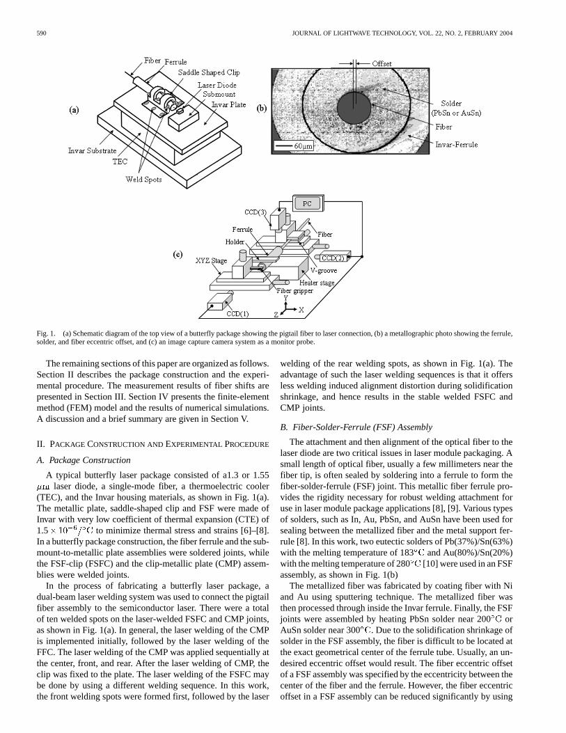
Fig. 1. (a) Schematic diagram of the top view of a butterfly package showing the pigtail fiber to laser connection, (b) a metallographic photo showing the ferrule,solder, and fiber eccentric offset, and (c) an image capture camera system as a monitor probe.
The remaining sections of this paper are organized as follows.Section II describes the package construction and the experi-mental procedure. The measurement results of fiber shifts arepresented in Section III. Section IV presents the finite-elementmethod (FEM) model and the results of numerical simulations.A discussion and a brief summary are given in Section V.
II. PACKAGE CONSTRUCTION AND EXPERIMENTAL PROCEDURE
A. Package Construction
A typical butterfly laser package consisted of a1.3 or 1.55laser diode, a single-mode fiber, a thermoelectric cooler
(TEC), and the Invar housing materials, as shown in Fig. 1(a).The metallic plate, saddle-shaped clip and FSF were made ofInvar with very low coefficient of thermal expansion (CTE) of1.5 to minimize thermal stress and strains [6]–[8].In a butterfly package construction, the fiber ferrule and the sub-mount-to-metallic plate assemblies were soldered joints, whilethe FSF-clip (FSFC) and the clip-metallic plate (CMP) assem-blies were welded joints.
In the process of fabricating a butterfly laser package, adual-beam laser welding system was used to connect the pigtailfiber assembly to the semiconductor laser. There were a totalof ten welded spots on the laser-welded FSFC and CMP joints,as shown in Fig. 1(a). In general, the laser welding of the CMPis implemented initially, followed by the laser welding of theFFC. The laser welding of the CMP was applied sequentially atthe center, front, and rear. After the laser welding of CMP, theclip was fixed to the plate. The laser welding of the FSFC maybe done by using a different welding sequence. In this work,the front welding spots were formed first, followed by the laser
welding of the rear welding spots, as shown in Fig. 1(a). Theadvantage of such the laser welding sequences is that it offersless welding induced alignment distortion during solidificationshrinkage, and hence results in the stable welded FSFC andCMP joints.
B. Fiber-Solder-Ferrule (FSF) Assembly
The attachment and then alignment of the optical fiber to thelaser diode are two critical issues in laser module packaging. Asmall length of optical fiber, usually a few millimeters near thefiber tip, is often sealed by soldering into a ferrule to form thefiber-solder-ferrule (FSF) joint. This metallic fiber ferrule pro-vides the rigidity necessary for robust welding attachment foruse in laser module package applications [8], [9]. Various typesof solders, such as In, Au, PbSn, and AuSn have been used forsealing between the metallized fiber and the metal support fer-rule [8]. In this work, two eutectic solders of Pb(37%)/Sn(63%)with the melting temperature of 183 and Au(80%)/Sn(20%)with the melting temperature of 280 [10] were used in an FSFassembly, as shown in Fig. 1(b)
The metallized fiber was fabricated by coating fiber with Niand Au using sputtering technique. The metallized fiber wasthen processed through inside the Invar ferrule. Finally, the FSFjoints were assembled by heating PbSn solder near 200 orAuSn solder near 300 . Due to the solidification shrinkage ofsolder in the FSF assembly, the fiber is difficult to be located atthe exact geometrical center of the ferrule tube. Usually, an un-desired eccentric offset would result. The fiber eccentric offsetof a FSF assembly was specified by the eccentricity between thecenter of the fiber and the ferrule. However, the fiber eccentricoffset in a FSF assembly can be reduced significantly by using
CHENG et al.: OPTIMUM APPROACH FOR REDUCTION OF FIBER ALIGNMENT SHIFT OF FSF JOINTS 591
an image capture camera system as a monitor probe, as shownin Fig. 1(b) for an 8 fiber eccentric offset.
C. An Image Capture Camera System
An image capture camera monitor system consisted of animage acquisition card, a computer, three charge-coupled de-vices (CCDs), and two stages, as shown in Fig. 1(c). Ametallized single-mode fiber (SMF) of 125 diameter and 1m long was inserted into the Invar ferrule of 400 inner diam-eter and 5 mm long. The front-end and rear-end fibers were heldby the fiber gripper and v-groove, respectively. Three CCD’swith a resolution of 640 480 pixels were used as the feedbacksensor to improve the position accuracy by capturing the imageof the FSF cross section and displaying the image processingresults on the monitor. The CCD 1) facing along the -axisfrom an end view was used to monitor the eccentric offset inthe front-end fiber, whereas the CCD 2) facing along the -axisand CCD 3) facing along the -axis from side views were usedto monitor the eccentric offset in the rear-end fiber, as shown inFig. 1(c). Using these three CCDs as a monitor probe, the fibercan be adjusted and moved to the center of the ferrule by using
stages according to the measured eccentric offsets.The Invar ferrule with the fiber and solder assembly was then
heated by a hot plate. While the fiber was sealed by solderingwith the ferrule to form the FSF joint, a homogenous temper-ature distribution along the Invar ferrule is essential in orderto maintain good wetting for solder flowing into the ferrule bysurface tension. In this case, a good solder joint of the FSF as-sembly was obtained. A pre-offset eccentricity of the fiber ofabout 10 in and -axis using the monitor system of theCCD (1), CCD (2), and CCD (3) may also be applied to com-pensate the thermal expansion of hot plate due to the heatingof the PbSn solder near 200 or the AuSn solder near 300 .Therefore, the fiber eccentric offset in a FSF assembly can be re-duced significantly by using the proposed image capture camerasystem as a monitor probe.
D. Temperature Cycling Test
The process of the temperature cycling test followed theprocedure proposed by the Bellcore Reliability AssurancePractices of TA-TSY-000983 [11]. During the temperaturecycle testing, the surrounding temperature was controlled from
to 85 with a cycle time of 40 min. The ramp ratewas greater than 10 /min and the dwell time was 30 minfor a total of 500 cycles. The fiber shifts were measured andrecorded after every 100 cycles.
III. MEASUREMENTS AND RESULTS
A. Fiber Alignment Shift Measurements
In this study, a novel metallographic technique using scratchlines in the FSF joints was used to provide reference marksfor the fiber alignment shift measurement [3], [4]. The scratchlines in the FSF assembly were due to the grinding and pol-ishing marks left by the metallographic preparation. The refer-ence coordinates were obtained by choosing the intersection oftwo scratch lines. Five reference coordinates were chosen as thefix references located on the ferrule to specify the fiber center
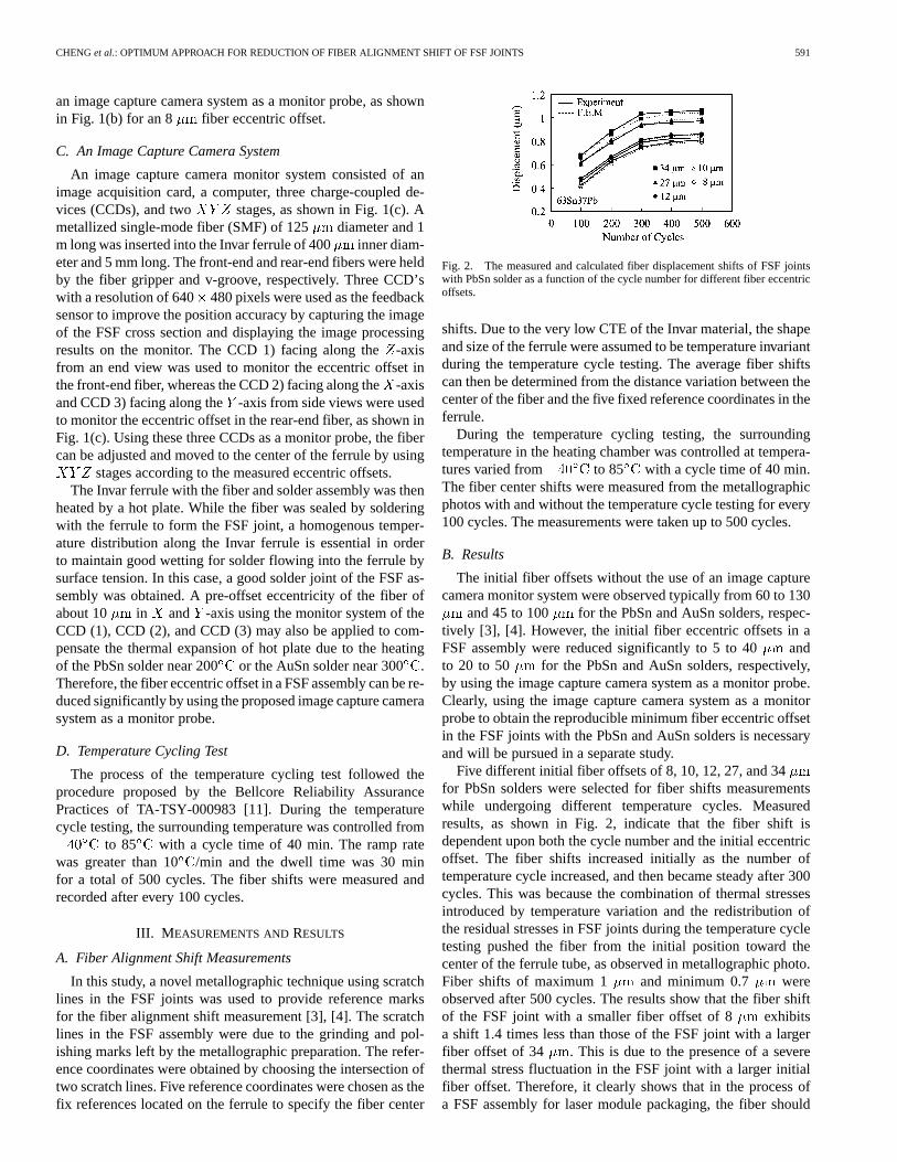
Fig. 2. The measured and calculated fiber displacement shifts of FSF jointswith PbSn solder as a function of the cycle number for different fiber eccentricoffsets.
shifts. Due to the very low CTE of the Invar material, the shapeand size of the ferrule were assumed to be temperature invariantduring the temperature cycle testing. The average fiber shiftscan then be determined from the distance variation between thecenter of the fiber and the five fixed reference coordinates in theferrule.
During the temperature cycling testing, the surroundingtemperature in the heating chamber was controlled at tempera-tures varied from to 85 with a cycle time of 40 min.The fiber center shifts were measured from the metallographicphotos with and without the temperature cycle testing for every100 cycles. The measurements were taken up to 500 cycles.
B. Results
The initial fiber offsets without the use of an image capturecamera monitor system were observed typically from 60 to 130
and 45 to 100 for the PbSn and AuSn solders, respec-tively [3], [4]. However, the initial fiber eccentric offsets in aFSF assembly were reduced significantly to 5 to 40 andto 20 to 50 for the PbSn and AuSn solders, respectively,by using the image capture camera system as a monitor probe.Clearly, using the image capture camera system as a monitorprobe to obtain the reproducible minimum fiber eccentric offsetin the FSF joints with the PbSn and AuSn solders is necessaryand will be pursued in a separate study.
Five different initial fiber offsets of 8, 10, 12, 27, and 34for PbSn solders were selected for fiber shifts measurementswhile undergoing different temperature cycles. Measuredresults, as shown in Fig. 2, indicate that the fiber shift isdependent upon both the cycle number and the initial eccentricoffset. The fiber shifts increased initially as the number oftemperature cycle increased, and then became steady after 300cycles. This was because the combination of thermal stressesintroduced by temperature variation and the redistribution ofthe residual stresses in FSF joints during the temperature cycletesting pushed the fiber from the initial position toward thecenter of the ferrule tube, as observed in metallographic photo.Fiber shifts of maximum 1 and minimum 0.7 wereobserved after 500 cycles. The results show that the fiber shiftof the FSF joint with a smaller fiber offset of 8 exhibitsa shift 1.4 times less than those of the FSF joint with a largerfiber offset of 34 . This is due to the presence of a severethermal stress fluctuation in the FSF joint with a larger initialfiber offset. Therefore, it clearly shows that in the process ofa FSF assembly for laser module packaging, the fiber should
592 JOURNAL OF LIGHTWAVE TECHNOLOGY, VOL. 22, NO. 2, FEBRUARY 2004
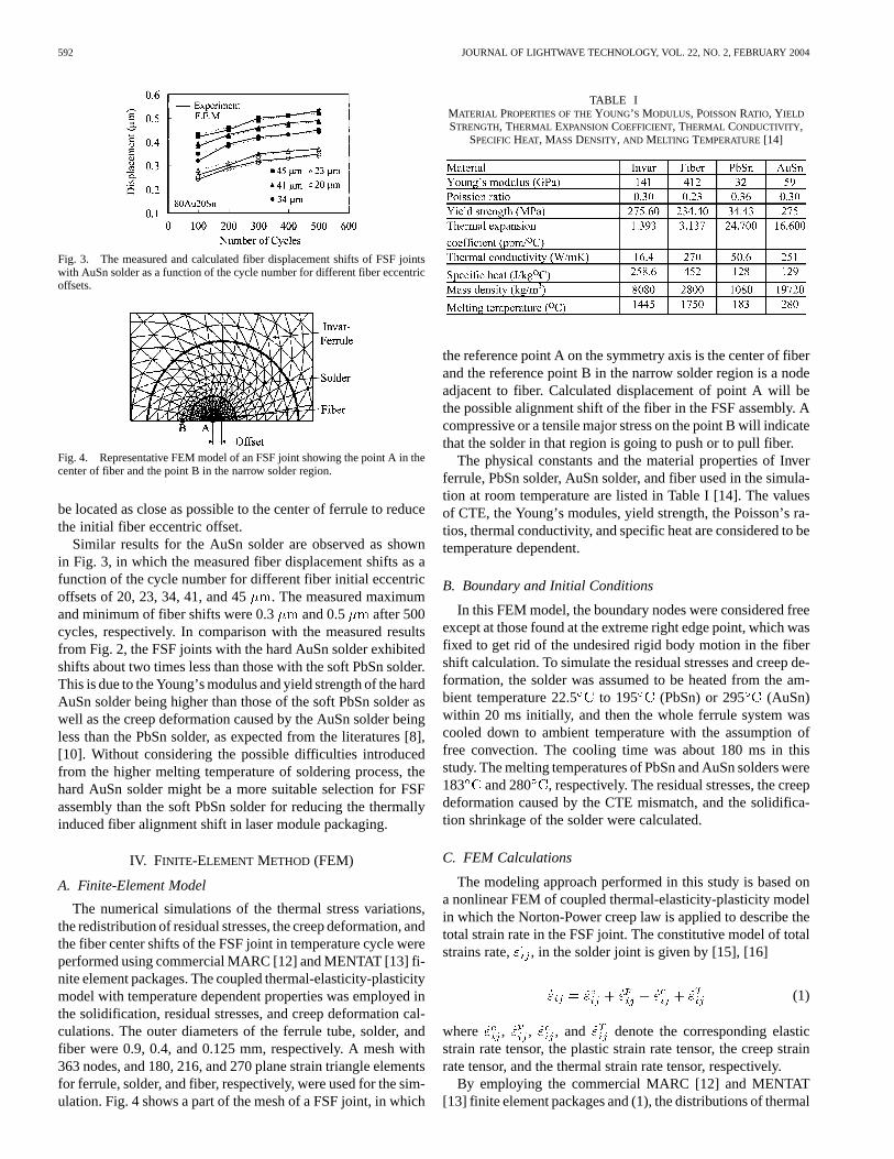
Fig. 3. The measured and calculated fiber displacement shifts of FSF jointswith AuSn solder as a function of the cycle number for different fiber eccentricoffsets.
Fig. 4. Representative FEM model of an FSF joint showing the point A in thecenter of fiber and the point B in the narrow solder region.
be located as close as possible to the center of ferrule to reducethe initial fiber eccentric offset.
Similar results for the AuSn solder are observed as shownin Fig. 3, in which the measured fiber displacement shifts as afunction of the cycle number for different fiber initial eccentricoffsets of 20, 23, 34, 41, and 45 . The measured maximumand minimum of fiber shifts were 0.3 and 0.5 after 500cycles, respectively. In comparison with the measured resultsfrom Fig. 2, the FSF joints with the hard AuSn solder exhibitedshifts about two times less than those with the soft PbSn solder.This is due to the Young’s modulus and yield strength of the hardAuSn solder being higher than those of the soft PbSn solder aswell as the creep deformation caused by the AuSn solder beingless than the PbSn solder, as expected from the literatures [8],[10]. Without considering the possible difficulties introducedfrom the higher melting temperature of soldering process, thehard AuSn solder might be a more suitable selection for FSFassembly than the soft PbSn solder for reducing the thermallyinduced fiber alignment shift in laser module packaging.
IV. FINITE-ELEMENT METHOD (FEM)
A. Finite-Element Model
The numerical simulations of the thermal stress variations,the redistribution of residual stresses, the creep deformation, andthe fiber center shifts of the FSF joint in temperature cycle wereperformed using commercial MARC [12] and MENTAT [13] fi-nite element packages. The coupled thermal-elasticity-plasticitymodel with temperature dependent properties was employed inthe solidification, residual stresses, and creep deformation cal-culations. The outer diameters of the ferrule tube, solder, andfiber were 0.9, 0.4, and 0.125 mm, respectively. A mesh with363 nodes, and 180, 216, and 270 plane strain triangle elementsfor ferrule, solder, and fiber, respectively, were used for the sim-ulation. Fig. 4 shows a part of the mesh of a FSF joint, in which
TABLE IMATERIAL PROPERTIES OF THE YOUNG’S MODULUS, POISSON RATIO, YIELD
STRENGTH, THERMAL EXPANSION COEFFICIENT, THERMAL CONDUCTIVITY,SPECIFIC HEAT, MASS DENSITY, AND MELTING TEMPERATURE [14]
the reference point A on the symmetry axis is the center of fiberand the reference point B in the narrow solder region is a nodeadjacent to fiber. Calculated displacement of point A will bethe possible alignment shift of the fiber in the FSF assembly. Acompressive or a tensile major stress on the point B will indicatethat the solder in that region is going to push or to pull fiber.
The physical constants and the material properties of Inverferrule, PbSn solder, AuSn solder, and fiber used in the simula-tion at room temperature are listed in Table I [14]. The valuesof CTE, the Young’s modules, yield strength, the Poisson’s ra-tios, thermal conductivity, and specific heat are considered to betemperature dependent.
B. Boundary and Initial Conditions
In this FEM model, the boundary nodes were considered freeexcept at those found at the extreme right edge point, which wasfixed to get rid of the undesired rigid body motion in the fibershift calculation. To simulate the residual stresses and creep de-formation, the solder was assumed to be heated from the am-bient temperature 22.5 to 195 (PbSn) or 295 (AuSn)within 20 ms initially, and then the whole ferrule system wascooled down to ambient temperature with the assumption offree convection. The cooling time was about 180 ms in thisstudy. The melting temperatures of PbSn and AuSn solders were183 and 280 , respectively. The residual stresses, the creepdeformation caused by the CTE mismatch, and the solidifica-tion shrinkage of the solder were calculated.
C. FEM Calculations
The modeling approach performed in this study is based ona nonlinear FEM of coupled thermal-elasticity-plasticity modelin which the Norton-Power creep law is applied to describe thetotal strain rate in the FSF joint. The constitutive model of totalstrains rate, , in the solder joint is given by [15], [16]
(1)
where , , , and denote the corresponding elasticstrain rate tensor, the plastic strain rate tensor, the creep strainrate tensor, and the thermal strain rate tensor, respectively.
By employing the commercial MARC [12] and MENTAT[13] finite element packages and (1), the distributions of thermal
CHENG et al.: OPTIMUM APPROACH FOR REDUCTION OF FIBER ALIGNMENT SHIFT OF FSF JOINTS 593
Fig. 5. Variations of the maximum principal stress as a function of temperaturecycle time of FSF joints at point B for PbSn solder with fiber eccentric offset of8 ��.
Fig. 6. Variations of the maximum principal stress as a function of temperaturecycle time of FSF joints at point B for AuSn solder with fiber eccentric offsetof 20 ��.
stresses, residual stresses, creep deformation, and fiber displace-ment shifts in the FSF joints were obtained [4], [17] and are pre-sented in Section IV-D.
D. Simulation Results
1) PbSn Solder: The variation of the major principal stressat point B of Fig. 4 during the temperature cycle testing is shownin Fig. 5. The result indicates that a residual stress up to 15.8MPa may be introduced at point B for the FSF joint with an8 initial fiber offset. Our results showed that the residualstress at point B varied from 15.8 MPa after solidification to 14.2(without considering creep deformation) and 11.2 MPa (withconsidering creep deformation) after undergoing 500 tempera-ture cycles. This indicates that an additional 19% of the stressrelaxation in the PbSn solder may be introduced in the FEMmodel if creep deformation is considered. Therefore, the stressrelaxation of creep deformation in the PbSn solder plays an im-portant role in the FSF joint for the deformation analyzes in tem-perature cycle testing.
Fig. 2 shows the fiber shifts calculated by the FEM model.The numerical results of the fiber shifts with PbSn solder werein good agreement with experimental measurements if both theresidual stresses and creep deformation within the solder wereconsidered.
2) AuSn Solder: Similar results were calculated for the FSFjoints with the AuSn solder. The variation of the stress peakswith the number of temperature cycles is shown in Fig. 6. Fig. 6indicates that a residual stress of 47.6 MPa was calculated atpoint B for the FSF joint with an initial offset of 20 . The cal-culated residual stresses at point B became 46.6 (without consid-ering creep deformation) and 45 MPa (with considering creep
deformation) after 500 cycle tests, as shown in Fig. 6. Only a3% difference was found for the AuSn joint. From the results ofFigs. 5 and 6, it can be seen that the FSF joints with the AuSnsolder exhibits a less creep effect than the PbSn solder, as ex-pected from the literatures [8], [10].
A comparison of calculated results in Figs. 5 and 6 indicatesthat the creep deformation effect in the AuSn joint simulation isnot as critical as the one in the PbSn joint simulation. A highermelting temperature of the solder is the key reason to make thecreep effect insignificant in the temperature cycle testing simu-lation of an AuSn solder joint. Fig. 3 also shows the variation ofthe fiber shifts of joints with the initial offsets of 20, 23, 34, 41,and 45 . An excellent agreement between the measured andcalculated data is shown in Fig. 3.
V. DISCUSSION AND CONCLUSION
We have demonstrated an optimum approach for the reduc-tion of fiber alignment shift of the fiber-solder-ferrule (FSF)joints in laser module packaging under temperature cyclingtesting by using a novel image capture camera system as a mon-itor probe and the Sn-based solders as bonding materials. Thenumerical calculations of fiber shifts were in good agreementwith the experimental measurements, if both the residual stressin solidification and the creep deformation in stress relaxationwithin solder were considered in the FEM model. The resultsof this study may be useful for fabricating reliable, high-yieldand high-performance laser module packages used in lightwavecommunication system applications. The following conclusionscan be drawn from the analysis which has been demonstratedin this study.
1) The numerical calculations of fiber shifts were in goodagreement with experimental measurements when boththe residual stresses and the creep deformation within thesolder were considered. This indicates that the proposedFEM model is an effective method for predicting the fiberalignment shifts in soldering joints.
2) The minimum of 8 and 20 and the maximum of 34and 45 for the initial fiber eccentric offsets of FSFjoints with the PbSn and AuSn solders, respectively, werefabricated by using an image capture camera system as amonitor probe.
3) The minimum of 0.7 and 0.3 and the maximum of 1and 0.5 for the fiber alignment shifts in FSF jointsusing the PbSn and AuSn solders, respectively, werefound after 500 temperature cycles testing. Comparisonbetween the measured results showed that the fiber shiftsof FSF joints with the hard AuSn solder exhibited shiftstwo times less than those with the soft PbSn solder.
4) Without considering the higher melting temperatureof soldering process, the hard AuSn solder might be amore suitable selection for FSF assembly than the softPbSn solder for reducing the thermally induced fiberalignment shift. This is due to the Young’s modulusand yield strength of the hard AuSn solder being higherthan those of the soft PbSn solder as well as the creepdeformation caused by the AuSn solder being less thanthe PbSn solder.
594 JOURNAL OF LIGHTWAVE TECHNOLOGY, VOL. 22, NO. 2, FEBRUARY 2004
5) An optimum approach for the reduction of the fiber align-ment shifts of FSF joints in laser module packages undertemperature cycling test was to solder the fiber near tothe center of the ferrule to reduce the initial fiber eccen-tric offsets and to select the AuSn hard solder for bettermaterial properties.
ACKNOWLEDGMENT
The authors would like to thank T. Y. Chang, S. Y. Huang,and J. H. Kuang of National Sun Yat-sen University for theirstimulation discussion and valuable suggestions of this work.
REFERENCES
[1] D. S. Alles, “Trends in laser packaging,” in Proc. 40th ECTC, 1990, pp.185–192.
[2] M. R. Matthews, B. M. Macdonald, and K. R. Preston, “Optical compo-nents-the new challenge in packaging,” IEEE Trans. Comp., Hybr. Man-ufact. Technol., vol. 3, pp. 798–806, 1990.
[3] W. H. Cheng, M. T. Sheen, C. P. Chien, H. L. Chang, and K. J. Kuang,“Reduction of fiber alignment shifts in laser module packaging,” J.Lightwave Technol., vol. 18, pp. 842–848, 2000.
[4] W. H. Cheng, M. T. Sheen, G. L. Wang, S. Z. Wang, and K. J. Kuang,“Fiber alignment shifts formation mechanisms of fiber-solder-ferrulejoints in laser module packaging,” J. Lightwave Technol., vol. 19, pp.1177–1184, 2001.
[5] C. Basaran and R. Chandaroy, “Finite element simulation of the temper-ature cycling tests,” IEEE Trans. Comp., Hybr. Manufact. Technol., vol.20, pp. 530–536, 1997.
[6] “Low-expansion alloys,” in Metals Handbook, 8th ed: ASM, 1973, vol.8, pp. 266–267.
[7] R. Chanchani and P. M. Hall, “Temperature dependence of thermal ex-pansion of ceramics and metals for electronic packages,” IEEE Trans.Comp., Hybr. Manufact. Technol., vol. 13, pp. 743–750, 1990.
[8] E. Suhir, “Thermally induced stresses in an optical glass fiber solderedinto a ferrule,” J. Lightwave Techol., vol. 12, pp. 1766–1770, 1994.
[9] W. H. Cheng, Y. D. Yang, S. C. Wang, S. Chi, M. T. Sheen, and J. H.Kuang, “Effect of Au thickness on laser beam penetration in semicon-ductor laser packages,” IEEE Trans. Comp., Hybr. Manufact. Technol.,vol. 20, pp. 396–402, 1997.
[10] A. R. Mickelson, N. R. Basavanhally, and Y. C. Lee, OptoelectronicPackaging. New York: Wiley, 1997, ch. 5.
[12] MARC 6.3,User Guide, MARC Analysis Research Corporation, PaloAlto, CA, 1996.
[13] MENTAL II, User Guide, MARC Analysis Research Corporation, PaloAlto, CA, 1996.
[14] J. H. Lau and Y. H. Pao, Solder Joint Reliability of BGA, CSP, Flip Chips,and Fine Pitxh SMT Assemblies. New York: McGraw-Hill, 1997, ch.4.
[15] T. Y. Pan, “Thermal cycling induced plastic deformation in solderjoints-part 1: Accumulated deformation in surface mount joints,” J.Electron. Packaging, vol. 113, pp. 8–15, 1991.
[16] B. Z. Hong and L. G. Burrell, “Nonlinear finite element simulationof thermoviscoplastic deformation of C4 solder joints in high densitypackaging under thermal cycling,” IEEE Trans. Comp., Hybr. Manufact.Technol.-Part A, vol. 18, pp. 585–591, 1995.
[17] M. T. Sheen, “A Study on Residual Stresses and Creep Deformationin Laser Module Packaging,” Ph.D. dissertation, Nattional Sun Yat-senUniversity, Taiwan, 2000.
Wood-Hi Cheng (M’95–SM’00) was born inChanghua, Taiwan, R.O.C., on June 3, 1944. Hereceived the Ph.D. degree in physics from OklahomaState University, Stillwater, in 1978.
From 1978 to 1980, he was a Research Associateat Telecommunication Laboratories, Taiwan. From1980 to 1984, he was a Research Engineer atGeneral Optronics, Edison, NJ. From 1984 to 1991,he was a Principal Design Engineer at RockwellInternational, Newbury Park, CA. From 1991 to1994, he was an Optoelectronic Packaging Manager
at Tacan Corporation. Carlsbad, CA. He is now a Professor at the Institute ofElectro-Optical Engineering and Dean of Engineering, National Sun Yat-senUniversity, Kaoshiung, Taiwan, R.O.C. His research and development activitieshave been focused on the design and fabrication of high-speed semiconductorlasers for lightwave communications, highly efficient light coupling from lasersand LEDs into fibers, fiber couplers, characterization of III–V semiconductorsmaterials, and optoelectronic packaging. His current research interests arethe design, fabrication, and finite-element method analysis for laser modulepackaging, high-speed laser module packaging for digital lightwave systems,novel materials for electromagnetic shielding, and fabrication of high densityWDM components. He served as a consultant for Chunghwa Telecom Labora-tories, Opto-Electronics and System Laboratories, and Chung-Shan Institute ofScience and Technology, all from Taiwan.
Dr. Cheng is a Member of the Optical Society of America (OSA) and thePhotonics Society of Chinese-Americans. He served as a Chair for the IEEELasers and Electro-Optics Society (LEOS), Taipei Chapter during 1999–2000,and serves as a Treasurer for the OSA, Taipei Chapter.
Maw-Tyan Sheen (M’03) received the B.S. andM.S. degrees in mechanical engineering fromNational Cheng Kung University, Tainan, Taiwan,R.O.C., in 1989 and 1994, respectively, and thePh.D. degree in mechanical engineering fromthe National Sun Yat-sen University, Kaoshiung,Taiwan, in 2000.
From 1994 to 1995, he was a teacher at Yang-MingHigh School, Tainan, Taiwan. From 2000 to 2003,he was a Research Associate with the Institute ofElectro-Optical Engineering, National Sun Yat-sen
University, Kaoshiung, Taiwan. He is currently an Assistant Professor at theDepartment of Electronic Engineering, Yung Ta Institute of Technology andCommerce, Ping-Tung, Taiwan. His research interests are OptoelectronicPackaging, laser welding technology for low-cost and high-speed lasermodules, and finite-element method for laser packaging.
Chia-Ming Chang received the B.S. degree in elec-trical engineering, in 1991, from Tatung University,Taipei, Taiwan, R.O.C., and the M.S. degree inelectro-optical engineering, in 2001, from NationalSun Yat-sen University, Kaohsiung, Taiwan, R.O.C.,where he is pursuing the Ph.D. degree.
He currently is a Test Engineer at Philips Semicon-ductor Kaohsiung, Kaohsiung, Taiwan. His researchinterests are optoelectronic packaging for telecom-munication applications.
Yih-Tun Tseng received the B.S. degree in mechan-ical engineering from National Taiwan University,Taipei, Taiwan, R.O.C., in 1971 and the Ph.D. degreein mechanical engineering from the University ofMichigan, Ann Arbor, in 1991.
He is currently is an Associate Professor with theDepartment of Mechanical and Electro-MechanicalEngineering, National Sun Yat-sen University,Kaoshiung, Taiwan. His primary research focuses inthe area of optoelectronic packaging automation.