20
TLE6389-x – Using the Demo Board TLE6389-2GV50 TLE6389-3GV50 TLE6389-2GV DC-DC Buck Converter Z8F52274261 Automotive Power Application Note Rev. 1.01, 2015-07-27
TLE6389-x – Using the Demo BoardTLE6389-2GV50TLE6389-3GV50TLE6389-2GV
DC-DC Buck ConverterZ8F52274261
Automotive Power
Application NoteRev. 1.01, 2015-07-27
TLE6389-x – Using the Demo BoardZ8F52274261
Application Note 2 Rev. 1.01, 2015-07-27
Table of Contents . . . . . . . . . . . . . . . . . . . . . . . . . . . . . . . . . . . . . . . . . . . . . . . . . . . . . . . . . . . . . . . . . 2
1 Abstract . . . . . . . . . . . . . . . . . . . . . . . . . . . . . . . . . . . . . . . . . . . . . . . . . . . . . . . . . . . . . . . . . . . . . . . . . 3
2 Introduction . . . . . . . . . . . . . . . . . . . . . . . . . . . . . . . . . . . . . . . . . . . . . . . . . . . . . . . . . . . . . . . . . . . . . 4
3 Application Schematic for 5 V Output Versions . . . . . . . . . . . . . . . . . . . . . . . . . . . . . . . . . . . . . . . . 53.1 Notes on the 5V Demo Boards . . . . . . . . . . . . . . . . . . . . . . . . . . . . . . . . . . . . . . . . . . . . . . . . . . . . . . . . . . . . . . .6
4 Application Circuit of the Variable Output Voltage Version . . . . . . . . . . . . . . . . . . . . . . . . . . . . . . 74.1 Notes on the Variable Voltage Demo Board . . . . . . . . . . . . . . . . . . . . . . . . . . . . . . . . . . . . . . . . . . . . . . . . . . .8
5 Dimensioning of the external components . . . . . . . . . . . . . . . . . . . . . . . . . . . . . . . . . . . . . . . . . . . 95.1 5 V-Versions . . . . . . . . . . . . . . . . . . . . . . . . . . . . . . . . . . . . . . . . . . . . . . . . . . . . . . . . . . . . . . . . . . . . . . . . . . . . . . .95.2 Variable Output Voltage . . . . . . . . . . . . . . . . . . . . . . . . . . . . . . . . . . . . . . . . . . . . . . . . . . . . . . . . . . . . . . . . . . .11
6 Components placement and PCB layout . . . . . . . . . . . . . . . . . . . . . . . . . . . . . . . . . . . . . . . . . . . . 13
7 Layout Recommendations . . . . . . . . . . . . . . . . . . . . . . . . . . . . . . . . . . . . . . . . . . . . . . . . . . . . . . . . 14
8 TLE6389 vs. TLE6389-2 and TLE6389-3 . . . . . . . . . . . . . . . . . . . . . . . . . . . . . . . . . . . . . . . . . . . . . . 16
9 Foldback Current Limitation . . . . . . . . . . . . . . . . . . . . . . . . . . . . . . . . . . . . . . . . . . . . . . . . . . . . . . 17
10 Additional Information . . . . . . . . . . . . . . . . . . . . . . . . . . . . . . . . . . . . . . . . . . . . . . . . . . . . . . . . . . . 18
11 Revision History . . . . . . . . . . . . . . . . . . . . . . . . . . . . . . . . . . . . . . . . . . . . . . . . . . . . . . . . . . . . . . . . . 19
Table of Contents

Application Note 3 Rev. 1.01, 2015-07-27
TLE6389-x – Using the Demo BoardZ8F52274261
Abstract
1 Abstract
Note: The following information is given as a hint for the implementation of the device only and shall not be regarded as a description or warranty of a certain functionality, condition or quality of the device.
This Application Note provides information on using the demo board of the switched mode regulators TLE6389-2GV50, TLE 6389-3GV50 and TLE 6389-2GV. The reader should be enabled to understand thedimensioning of the components and change them in order to adapt the function for his application needs.

Application Note 4 Rev. 1.01, 2015-07-27
TLE6389-x – Using the Demo BoardZ8F52274261
Introduction
2 IntroductionSelection of appropriate external components as well as the layout of the PCB is a key factor when designingDC-DC applications in automotive environment. The goal is to achieve optimum functionality with minimumoutput voltage ripple and good EMC performance. This application note gives a proposal for selectingcomponents and recommendations for layout with an example.
Figure 1 Demo Board with the TLE 63689-2GV50

Application Note 5 Rev. 1.01, 2015-07-27
TLE6389-x – Using the Demo BoardZ8F52274261
Application Schematic for 5 V Output Versions
3 Application Schematic for 5 V Output VersionsFigure 2 shows the minimum application circuit as proposed in the TLE6389 datas heet which applies for to5 V output versions TLE6389-2GV50 and TLE6389-3GV50.
Figure 2 Minimum Application Circuit for TLE6389-2GV50 and TLE6389-3GV50
The circuitry of the demo board is extended slightly. Figure 3 shows the complete circuitry of the demo board. The circuitry of the demo board ...• covers a wider load current range• improves EMC performance• allows using only one PCB, also applicable for the variable device TLE6389-2GV (see Chapter 4).
Figure 3 Schematic of the Demo Board for TLE6389-2GV50 and TLE6389-3GV50

Application Note 6 Rev. 1.01, 2015-07-27
TLE6389-x – Using the Demo BoardZ8F52274261
Application Schematic for 5 V Output Versions
3.1 Notes on the 5V Demo BoardsTLE6389-2GV50 and TLE6389-3GV50 have an integrated pull up resistor of typically 20 kΩ at the outputs ROand SO. The integrated pull up resistor connects RO, respectively SO, to the 5 V output voltage present at theVOUT pin. Therefore the resistors R12 and R13 are optional for these devices. On the demo board theseresistors are connected to the VEXT connector. The VEXT connector can be left open. In case a reduced pull upresistance is desired, VEXT can be connected externally to VOUT. VEXT should not be connected to othervoltage sources. The synchronizing function is disabled by the 0ΩΩ resistor R8 connecting pin 5 directly toGND. In case the synchronizing function is needed make sure R8 is removed before connecting a TTL-Levelfrequency source to the SYNC connector of the demo board. On the demo board the feedback input FB isconnected via R4 (0 Ω) to the output voltage, whereas the basic circuitry shows an open FB pin. The feedbackpin connection is optional for the 5 V devices since the voltage feedback of the error amplifier is connected tothe VOUT pin in the TLE6389-2GV50 and TLE6389-3GV50.
Table 1 Recommended Components - BOM for TLE6389-2GV50 and TLE6389-3GV50Device Supplier Type Value & RemarkL1 Coilcraft DO-3340P-333 33 µH, 2.0 A, 80 mΩ
L2 Coilcraft DO-3340P-223 22 µH, 2.5 A, 66 mΩ
C1 Various Al-Electrolytic capacitor 100 µF, 63 V
C2 Ceramic capacitor X7R, 100 nF, > 60 V1)
1) Mounted on PCB back side
C3 Ceramic capacitor X7R, 2.2 nF, 16 V
C4_1, C4_2 TDK Ceramic capacitor C4532X7R1H475M X7R, 4.7 µF, 50 V
C5 EPCOS Tantalum electrolytic capacitor B45010D1076M506 Low ESR, ‘Speed Power’
C6 Ceramic capacitor X7R, 100 nF, 16 V
C7 TDK Ceramic capacitor C3216X7R2A224 X7R, 220 nF, 100 V
C8 various Ceramic capacitor X7R, 220 nF, 16 V
C9 not assembled
R1 Resistor 22 mΩ, ±1 %
R2, R4, R6, R8 0 Ω
R3 Resistor 68 0Ω
R5, R7, R9 not assembled
R10 Resistor 68 Ω
R11 Resistor 390 Ω
R12, R13 Resistor 5.1 Ω
D1 ON Schottky Diode MBRD 360, 3 A, 60 V
D2 various Diode, S3D 3 A
M1 P-channel MOSFET BSP 613P2)
2) Pin 2 (GND) to be cut before assembly on demo board

Application Note 7 Rev. 1.01, 2015-07-27
TLE6389-x – Using the Demo BoardZ8F52274261
Application Circuit of the Variable Output Voltage Version
4 Application Circuit of the Variable Output Voltage VersionTLE6389-2GV shows the minimum application circuit as proposed in the TLE6389 data sheet for the variableoutput voltage version TLE6389-2GV.
Figure 4 Minimum Application Circuit for TLE6389-2GV
Similar to the fixed 5 V output voltage version, the circuitry of the TLE6389-2GV demo board is extendedslightly. Thus a wider load current range and improved EMC performance of the application can be achieved.Figure 5 shows the schematic of the demo board.
Figure 5 Schematic of the Demo Board for TLE 6389-2GV

Application Note 8 Rev. 1.01, 2015-07-27
TLE6389-x – Using the Demo BoardZ8F52274261
Application Circuit of the Variable Output Voltage Version
4.1 Notes on the Variable Voltage Demo BoardThe TLE6389-2GV has open drain outputs at the pins RO and SO. The pull up resistors R12 and R13 on the demoboard are connected to the V_EXT pad. V_EXT should be connected to an appropriate pull up voltage source(usually the microcontroller I/O voltage source). The pull up resistors have a value of R11 = R12 = 5.1 kΩ. Thisresistor value should be checked in respect to the actual I/O voltage and microcontroller requirements. Thedriving capability of the reset output and sense output are described in the data sheet (electricalcharacteristics, items 4.52, 4.53, 4.69 and 4.70). The synchronizing function is disabled by the 0 Ω resistor R8 connecting pin 5 directly to GND. In case thesynchronizing function is needed, make sure R8 is removed before connecting a TTL frequency source tothe SYNC connector of the demo board.
Table 2 Components recommendation - BOM for TLE 6389-2GVDevice Supplier Type Value & RemarkL1 Coilcraft DO-3340P-333 33 µH, 2.0 A, 80 mΩ
L2 Coilcraft DO-3340P-223 22 µH, 2.5 A, 66 mΩ
C1 Various Al-Electrolytic capacitor 100 µF, 63 V
C2 Ceramic capacitor X7R, 100 nF, > 60 V1)
1) Pin 2 (GND) to be cut before assembly on demo board
C3 Ceramic capacitor X7R, 2.2 nF, 16 V
C4_1, C4_2 TDK Ceramic capacitor C4532X7R1H475M X7R, 4.7 µF, 50 V
C5 EPCOS Tantalum electrolytic capacitor B45010D1076M506 Low ESR, ‘Speed Power’
C6 Ceramic capacitor X7R, 100 nF, 16 V
C7 TDK Ceramic capacitor C3216X7R2A224 X7R, 220 nF, 100 V
C8 various Ceramic capacitor X7R, 220 nF, 16 V
C9 not assembled
R1 Resistor 22 mΩ, ±1 %
R2, R4, R6, R8 0 Ω
R3 Resistor 680 Ω
R5, R7, R9 not assembled
R10 Resistor 68 Ω
R11 Resistor 390 Ω
R12, R13 Resistor 5. 1Ω
D1 ON Schottky Diode MBRD 360, 3 A, 60 V
D2 various Diode, S3D 3 A
M1 P-channel MOSFET BSP 613P1)

Application Note 9 Rev. 1.01, 2015-07-27
TLE6389-x – Using the Demo BoardZ8F52274261
Dimensioning of the external components
5 Dimensioning of the external componentsThe equations for dimensioning of the external components L1, R1 are given in the data sheet in chapter 7.Data sheet, chapter 7 also discusses the dimensioning of the feedback divider resistors R4 and R5. This Application Note shows a practical approach on how to apply these equations for given applicationrequirements.
5.1 5 V-VersionsThe maximum operating supply voltage at VBAT connector of the application board should be up to 58 V.Therefore all components connected to VBAT have to withstand 60 V, leaving some room for voltage ripplecaused by switching: C1, C4 (sum of rated voltage C4_1 +C4_2), C7, M1, D1. In the first step the right value of the current sensing shunt resistor R1 is determined. The application board isdesigned to supply a permanent output current of up to 2.0 A at 13.5 V input voltage with a target current of1.0 A. The (worst case = lowest) maximum current of 2.0 A is allowed to be in the foldback range of the outputcurrent characteristic (see Fig. 5). The data sheet, chapter 7.10.2 delivers the equation:
(5.1)
VLIM is specified in the electrical characteristics as item 4.36 ‘peak current limit threshold voltage’,50 mV …. 90 mV. To get the worst case (lowest) current the equation above is used, but without the factor 2,as entering the foldback part of the current characteristic is accepted:
(5.2)
Figure 6 Example of Typical Characteristics of the Output Current Limit (Foldback)
R1 = VLIM
2 × IPeak,PWM
R1max = 50 mV
2.0 A = 25 mΩ

Application Note 10 Rev. 1.01, 2015-07-27
TLE6389-x – Using the Demo BoardZ8F52274261
Dimensioning of the external components
The following equation takes into account the current ripple which reduces the maximum load currentavailable:
(5.3)
In the next step R1 is selected:
(5.4)
Using this value, the maximum current ripple allowed can be calculated, still assuming a load current of 2.0 A:
(5.5)
In order to keep the output voltage ripple as low as possible, a current ripple of 300 mA in the typical operationcondition with 13.5 V VBAT is chosen, corresponding to 15 % of the 2.0 A maximum load current. The datasheet, chapter 7.10.1 delivers the following equation:
(5.6)
This equation is now used to define the buck inductance L1:
(5.7)
A matching IEC 60063 E6 value is selected:
(5.8)
The following equation serves to check if the stability conditions arising from the slope compensation arefulfilled:
(5.9)
The result matches the allowed range of 500 Ω/H to 1000 Ω/H (data sheet, chapter 7.10.1).
IPeak,PWM = ILOAD + 0.5 × ∆I
R1 = 22 mΩ
∆Imax= 50 mV/22 mΩ − 2.0 A
0.5 = 545 mA
∆I = (V
IN− VOUT) × VOUT
fSW × VIN × L1
L1 = (13.5 V − 5.0 V) × 5.0 V
370 kHz × 13.5 V × 300 mA = 28 μH
L1 = 33 μH
RSENSE
L1 = 667 ΩH-1

Application Note 11 Rev. 1.01, 2015-07-27
TLE6389-x – Using the Demo BoardZ8F52274261
Dimensioning of the external components
5.2 Variable Output VoltageFor the TLE6389-2GV variable device demo board we use the same output current target as for the fixedvoltage version: 2.0 A, with permission to be in the foldback current limit range (see Fig. 5). The desired outputvoltage should be typically 7.10 V.Now the feedback output voltage divider should be fixed. The data sheet (chapter 7.3) allows a range from5 kΩ to 500 kΩ for R5 (corresponds to RFB2) of 5 kΩ to 500 kΩ. We have selected a value of R5 = 47 kΩ.R4 can be calculated using the feedback voltage value of 1.25 V (item 4.17 of the electrical characteristics inthe data sheet):
(5.10)
The following procedure is quite the same as for dimensioning the 5 V versions . The shunt resistor is given bythe current limitation target. The data sheet, chapter 7.10.2 provides the following equation:
(5.11)
VLIM is specified in the electrical characteristics as item 4.36 ‘peak current limit threshold voltage’,50 mV …. 90 mV. To get the worst case (lowest) current the equation above is used, but without the factor 2,as entering the foldback part of the current characteristic is accepted:
(5.12)
The following equation takes into account the current ripple which reduces the maximum load currentavailable:
(5.13)
In the next step R1 is selected:
(5.14)
Using this value, the maximum current ripple allowed can be calculated, still assuming a load current of 2.0 A:
(5.15)
R4 = 47 kΩ × (7.10 V
1.25 V − 1) = 220 kΩ
R1 = VLIM
2 × IPeak,PWM
R1max = 50 mV
2.0 A = 25 mΩ
IPeak,PWM = ILOAD + 0.5 × ∆I
R1 = 22 mΩ
∆Imax= 50 mV/22 mΩ − 2.0 A
0.5 = 545 mA

Application Note 12 Rev. 1.01, 2015-07-27
TLE6389-x – Using the Demo BoardZ8F52274261
Dimensioning of the external components
In order to keep the output voltage ripple as low as possible, a current ripple of 300 mA in the typical operationcondition with 13.5 V VBAT is chosen, corresponding to 15 % of the 2.0 A maximum load current. The datasheet, chapter 7.10.1 delivers the following equation:
(5.16)
This equation is now used to define the buck inductance L1:
(5.17)
The best matching IEC 60063 E6 value is selected:
(5.18)
The following inequation serves to check if the stability conditions arising from the slope compensation arefulfilled:
(5.19)
Thus, the inductance selected is good for maintaining stability.
∆I = (V
IN− VOUT) × VOUT
fSW × VIN × L1
L1 = (13.5 V − 5.0 V) × 5.0 V
370 kHz × 13.5 V × 300 mA = 28 μH
L1 = 33 μH
[(2.0 × 10⁻⁴ s
V) × VOUT × RSENSE] < L1 < [(4.0 × 10⁻⁴
s
V) × VOUT × RSENSE]
[(2.0 × 10⁻⁴ s
V) × 7.1 V × 22 mΩ] < L1 < [(4.0 × 10⁻⁴
s
V) × 7.1 V × 22 mΩ]
31 μH < L1 < 62 μH

Application Note 13 Rev. 1.01, 2015-07-24
TLE6389-x – Using the Demo BoardZ8F52274261
Components placement and PCB layout
6 Components placement and PCB layoutFor EMC optimization the demo board comes with an input Π-Filter (C4, L2, C1). Thus emission from the VBATline is largely suppressed. For both proper operation and avoiding stray inductance paths, the external catch diode, the Buck inductanceand the input capacitor CIN1 have to be connected to the PMOS device as close as possible. Also the path fromthe GDRV pin of the controller to the switching transistor should be as short as possible. A small area locatednext to the drain of the PMOS is best suitable for the connection of the catch diode’s cathode to one terminalof the inductance. The GND connection of the catch diode also must be as short as possible. In general the GND level should beimplemented as surface area over the whole PCB in a second layer. The most sensitive points to coupled switching noise are the feedback path to the pins FB and VOUT and theinput path. Switching noise coupled back to the SYNC input must be avoided also. These paths should be keptaway from the switching node. On the demo board also the ceramic capacitor C6 helps suppress potentialnoise on the feedback line.
Figure 7 PCB Layout
Application Note 14 Rev. 1.01, 2015-07-27
TLE6389-x – Using the Demo BoardZ8F52274261
Layout Recommendations
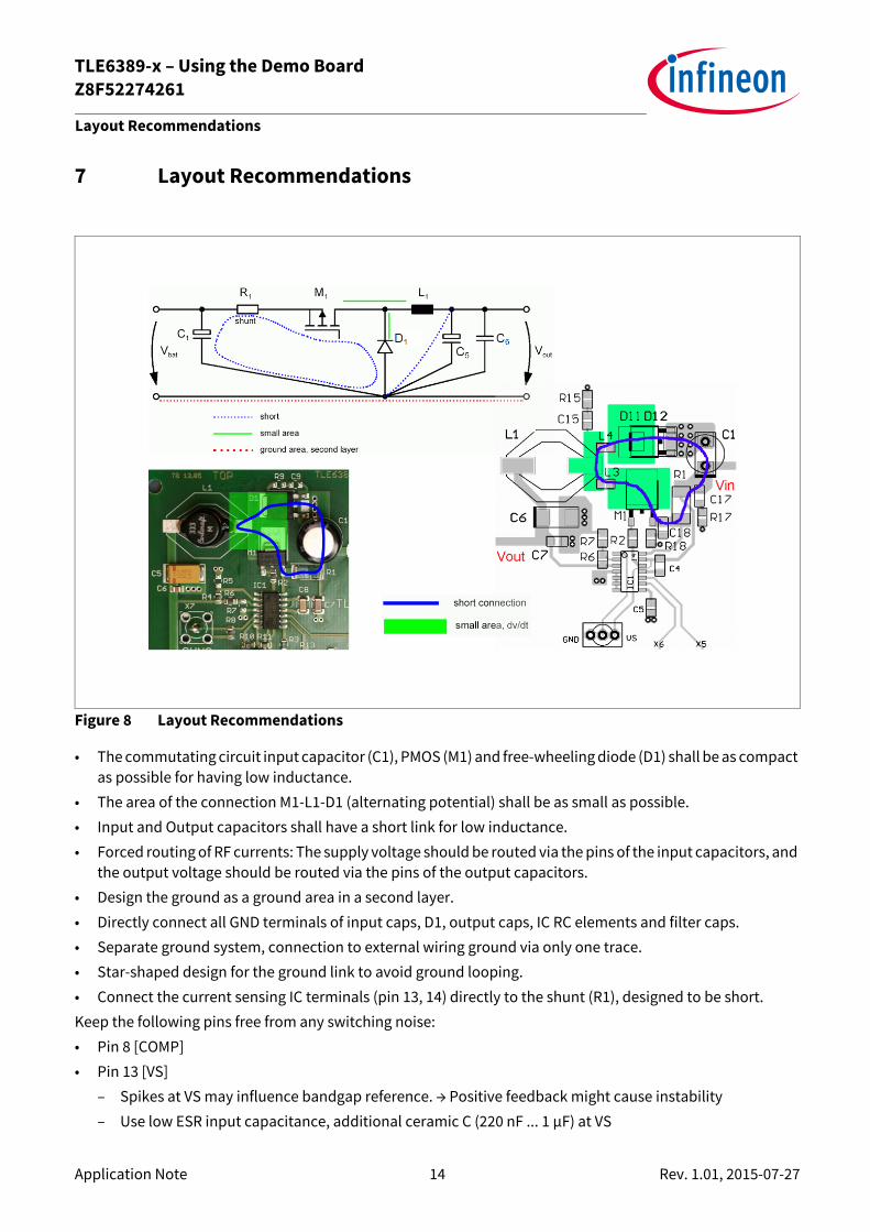
7 Layout Recommendations
Figure 8 Layout Recommendations
• The commutating circuit input capacitor (C1), PMOS (M1) and free-wheeling diode (D1) shall be as compact as possible for having low inductance.
• The area of the connection M1-L1-D1 (alternating potential) shall be as small as possible. • Input and Output capacitors shall have a short link for low inductance. • Forced routing of RF currents: The supply voltage should be routed via the pins of the input capacitors, and
the output voltage should be routed via the pins of the output capacitors. • Design the ground as a ground area in a second layer. • Directly connect all GND terminals of input caps, D1, output caps, IC RC elements and filter caps. • Separate ground system, connection to external wiring ground via only one trace. • Star-shaped design for the ground link to avoid ground looping. • Connect the current sensing IC terminals (pin 13, 14) directly to the shunt (R1), designed to be short. Keep the following pins free from any switching noise: • Pin 8 [COMP]• Pin 13 [VS]
– Spikes at VS may influence bandgap reference. → Positive feedback might cause instability– Use low ESR input capacitance, additional ceramic C (220 nF ... 1 µF) at VS

Application Note 15 Rev. 1.01, 2015-07-27
TLE6389-x – Using the Demo BoardZ8F52274261
Layout Recommendations
• Pin 2 [FB]– Keep PCB traces far from switching nodes to prevent from coupled switching noise– Use low-ESR output capacitance, additional ceramic recommended
• Pin 2 [VOUT]– Use low-ESR output capacitance, additional ceramic recommended
• Pin 5 [SYNC]
Application Note 16 Rev. 1.01, 2015-07-27
TLE6389-x – Using the Demo BoardZ8F52274261
TLE6389 vs. TLE6389-2 and TLE6389-3
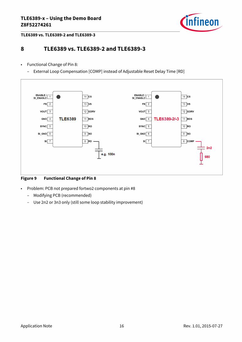
8 TLE6389 vs. TLE6389-2 and TLE6389-3
• Functional Change of Pin 8: – External Loop Compensation [COMP] instead of Adjustable Reset Delay Time [RD]
Figure 9 Functional Change of Pin 8
• Problem: PCB not prepared fortwo2 components at pin #8– Modifying PCB (recommended)– Use 2n2 or 3n3 only (still some loop stability improvement)

Application Note 17 Rev. 1.01, 2015-07-27
TLE6389-x – Using the Demo BoardZ8F52274261
Foldback Current Limitation
9 Foldback Current Limitation
Figure 10 Foldback Current Limitation
• Safe Operation:– IMAX ≥ (2 × INOM) → RSENSE = VLIM / (2 × IPeak,PWM)
• Assuming that the load current at reset condition is only half of the nominal output current– RSENSE = VLIM / IPeak,PWM

Application Note 18 Rev. 1.01, 2015-07-27
TLE6389-x – Using the Demo BoardZ8F52274261
Additional Information
10 Additional Information
• For further information you may contract http://www.infineon.com/

Application Note 19 Rev. 1.01, 2015-07-27
TLE6389-x – Using the Demo BoardZ8F52274261
Revision History
11 Revision History
Revision Date Changes1.01 2015-07-27 Infineon Style Guide update.
Editorial changes.
1.0 2006-08-31 Application Note initial revision.

Trademarks of Infineon Technologies AGAURIX™, C166™, CanPAK™, CIPOS™, CIPURSE™, CoolGaN™, CoolMOS™, CoolSET™, CoolSiC™, CORECONTROL™, CROSSAVE™, DAVE™, DI-POL™, DrBLADE™,EasyPIM™, EconoBRIDGE™, EconoDUAL™, EconoPACK™, EconoPIM™, EiceDRIVER™, eupec™, FCOS™, HITFET™, HybridPACK™, ISOFACE™, IsoPACK™, i-Wafer™, MIPAQ™, ModSTACK™, my-d™, NovalithIC™, OmniTune™, OPTIGA™, OptiMOS™, ORIGA™, POWERCODE™, PRIMARION™, PrimePACK™,PrimeSTACK™, PROFET™, PRO-SIL™, RASIC™, REAL3™, ReverSave™, SatRIC™, SIEGET™, SIPMOS™, SmartLEWIS™, SOLID FLASH™, SPOC™, TEMPFET™,thinQ!™, TRENCHSTOP™, TriCore™.Other TrademarksAdvance Design System™ (ADS) of Agilent Technologies, AMBA™, ARM™, MULTI-ICE™, KEIL™, PRIMECELL™, REALVIEW™, THUMB™, µVision™ of ARM Limited,UK. ANSI™ of American National Standards Institute. AUTOSAR™ of AUTOSAR development partnership. Bluetooth™ of Bluetooth SIG Inc. CAT-iq™ of DECTForum. COLOSSUS™, FirstGPS™ of Trimble Navigation Ltd. EMV™ of EMVCo, LLC (Visa Holdings Inc.). EPCOS™ of Epcos AG. FLEXGO™ of MicrosoftCorporation. HYPERTERMINAL™ of Hilgraeve Incorporated. MCS™ of Intel Corp. IEC™ of Commission Electrotechnique Internationale. IrDA™ of Infrared DataAssociation Corporation. ISO™ of INTERNATIONAL ORGANIZATION FOR STANDARDIZATION. MATLAB™ of MathWorks, Inc. MAXIM™ of Maxim IntegratedProducts, Inc. MICROTEC™, NUCLEUS™ of Mentor Graphics Corporation. MIPI™ of MIPI Alliance, Inc. MIPS™ of MIPS Technologies, Inc., USA. muRata™ ofMURATA MANUFACTURING CO., MICROWAVE OFFICE™ (MWO) of Applied Wave Research Inc., OmniVision™ of OmniVision Technologies, Inc. Openwave™ ofOpenwave Systems Inc. RED HAT™ of Red Hat, Inc. RFMD™ of RF Micro Devices, Inc. SIRIUS™ of Sirius Satellite Radio Inc. SOLARIS™ of Sun Microsystems, Inc.SPANSION™ of Spansion LLC Ltd. Symbian™ of Symbian Software Limited. TAIYO YUDEN™ of Taiyo Yuden Co. TEAKLITE™ of CEVA, Inc. TEKTRONIX™ ofTektronix Inc. TOKO™ of TOKO KABUSHIKI KAISHA TA. UNIX™ of X/Open Company Limited. VERILOG™, PALLADIUM™ of Cadence Design Systems, Inc.VLYNQ™ of Texas Instruments Incorporated. VXWORKS™, WIND RIVER™ of WIND RIVER SYSTEMS, INC. ZETEX™ of Diodes Zetex Limited.
Trademarks Update 2014-07-17
www.infineon.com
Edition 2015-07-27Published by Infineon Technologies AG81726 Munich, Germany
© 2014 Infineon Technologies AG.All Rights Reserved.
Do you have a question about any aspect of this document?Email: [email protected]
Document referenceDoc_Number
Legal DisclaimerTHE INFORMATION GIVEN IN THIS APPLICATION NOTE(INCLUDING BUT NOT LIMITED TO CONTENTS OFREFERENCED WEBSITES) IS GIVEN AS A HINT FOR THEIMPLEMENTATION OF THE INFINEON TECHNOLOGIESCOMPONENT ONLY AND SHALL NOT BE REGARDED ASANY DESCRIPTION OR WARRANTY OF A CERTAINFUNCTIONALITY, CONDITION OR QUALITY OF THEINFINEON TECHNOLOGIES COMPONENT. THERECIPIENT OF THIS APPLICATION NOTE MUST VERIFYANY FUNCTION DESCRIBED HEREIN IN THE REALAPPLICATION. INFINEON TECHNOLOGIES HEREBYDISCLAIMS ANY AND ALL WARRANTIES ANDLIABILITIES OF ANY KIND (INCLUDING WITHOUTLIMITATION WARRANTIES OF NON-INFRINGEMENT OFINTELLECTUAL PROPERTY RIGHTS OF ANY THIRDPARTY) WITH RESPECT TO ANY AND ALL INFORMATIONGIVEN IN THIS APPLICATION NOTE.
InformationFor further information on technology, delivery termsand conditions and prices, please contact the nearestInfineon Technologies Office (www.infineon.com).WarningsDue to technical requirements, components maycontain dangerous substances. For information on thetypes in question, please contact the nearest InfineonTechnologies Office. Infineon Technologiescomponents may be used in life-support devices orsystems only with the express written approval ofInfineon Technologies, if a failure of such componentscan reasonably be expected to cause the failure of thatlife-support device or system or to affect the safety oreffectiveness of that device or system. Life supportdevices or systems are intended to be implanted in thehuman body or to support and/or maintain andsustain and/or protect human life. If they fail, it isreasonable to assume that the health of the user orother persons may be endangered.


