1 / 16 2018-10-12 | Document No.: AN026 www.osram-os.com Application Note Manual lead-free soldering of LEDs from OSRAM Opto Semiconductors Abstract In addition to a brief fundamental consideration of the manual lead-free and lead-containing soldering process, this application note describes the essential influencing factors and their effect on the lead-free soldering process. Furthermore, the basic rules and specific guidelines associated with the manual lead-free soldering process are illustrated. Also, possible risks are discussed and the general procedure of the lead-free soldering process is described. In conclusion, an overview of the solderability of the various LED types from OSRAM Opto Semiconductors is presented, along with their ability to be reworked and repaired. Valid for: all OSRAM Opto Semiconductors LEDs Authors: Bartling Hanna / Lang Kurt-Jürgen Application Note No. AN026
Transcript
1 / 162018-10-12 | Document No.: AN026
www.osram-os.com
Application Note
Manual lead-free soldering of LEDs from OSRAM Opto Semiconductors
Abstract
In addition to a brief fundamental consideration of the manual lead-free and lead-containingsoldering process, this application note describes the essential influencing factors and theireffect on the lead-free soldering process.
Furthermore, the basic rules and specific guidelines associated with the manual lead-freesoldering process are illustrated. Also, possible risks are discussed and the generalprocedure of the lead-free soldering process is described.
In conclusion, an overview of the solderability of the various LED types from OSRAM OptoSemiconductors is presented, along with their ability to be reworked and repaired.
Valid for:all OSRAM Opto Semiconductors LEDs
Authors: Bartling Hanna / Lang Kurt-Jürgen
Application Note No. AN026
www.osram-os.com
Table of contents
A. Introduction .............................................................................................................2
B. Underlying considerations ......................................................................................3
C. Important influencing factors and their implications ..............................................4
Important LED-specific points ..........................................................................12
G. Conclusion ............................................................................................................14
A. Introduction
With the introduction and ratification of Directive 2002/95 (RoHS directive “onthe restriction of the use of certain hazardous substances in electrical andelectronic devices”) in June 2006, many production lines have switched to lead-free, RoHS-conformant technologies.
In automated production sequences, the implementation of lead-free solderingprocesses has been carried out without huge difficulties, despite of the smallerprocessing window due to the higher melting temperature of the new solder.
2 / 162018-10-12 | Document No.: AN026
www.osram-os.com
The quality, reproducibility and process stability has achieved an equally highlevel, although the solder heat resistance of individual SMD components such asLEDs makes it difficult to conform to the lead-free soldering process.
In contrast, the introduction of a manual lead-free soldering process is stillchallenging, as it is more difficult to control.
Today, manual soldering is almost exclusively used for the manufacture ofprototypes and for repair or rework of production components, qualityassurance represents the largest challenge, here.
With manual lead-free soldering, the quality is essentially influenced anddetermined by the solder materials and equipment, the experience and ability ofthe operator and a continuous process control.
It is therefore recommended to only carry out manual lead-free soldering withappropriate equipment and trained personnel.
In addition, it should be noted than not all available LED types are suited formanual soldering or repair.
B. Underlying considerations
In principle, manual soldering with lead-free solder is not much more difficultthan soldering with lead-containing solder. In order to achieve good results andgood solder connections, the properties and differences of the two solderingprocesses must be thoroughly understood and considered from a technicalstandpoint.
The essential differences between lead-free solder and tin-lead compounds isfirst of all, the higher melting temperature (up to 40 °C higher than tin-leadcompounds, depending on the solder used), and secondly, the poorer wettingcharacteristic of lead-free solders. For soldering, this means that the timerequired for wetting the solder joints increases and the lead-free solder takeslonger to spread. In addition, differences can arise in the appearance of thesolder joints; lead-free connections appear to be dull and matt (without luster) incomparison to lead-containing solder connections.
The quality and steadiness of soldering created manually with a soldering iron isgenerally influenced by several factors, including:
• Composition of the solder
• Activity of the flux material
• Thermal characteristics of the soldering iron
• Angle of soldering, dependent on the handling of the operator
• Joint clearance of the two surfaces
In addition to the above mentioned factors, the solder connection is ultimatelydependent on the prevailing temperature and effective time.
3 / 162018-10-12 | Document No.: AN026
www.osram-os.com
Figure 1: Different appearance of lead-containing (SnPb) and lead-free (SnAgCu) solder
C. Important influencing factors and their implications
Solder
The type of solder used represents the most important parameter and has adecisive influence on the entire soldering process and on the subsequentconnection.
Through the composition of the solder and the associated properties such assolder temperature, wetting and oxidation characteristics etc, a certain processwindow for the soldering process is predefined.
Figure 2: Side by side comparison of the process windows — lead-containing vs. lead-free
SnPb alloy SnAgCu alloy
205 °C
260 °C
235 °C
260 °C
Damage level LED Damage level LED
Process areaProcess area
Low temperature Low temperature
Lead-containing solderSnPb solder alloy183 °C - 210 °C
Lead-free solderSnAgCu solder alloy
221 °C - 227 °C
4 / 162018-10-12 | Document No.: AN026
www.osram-os.com
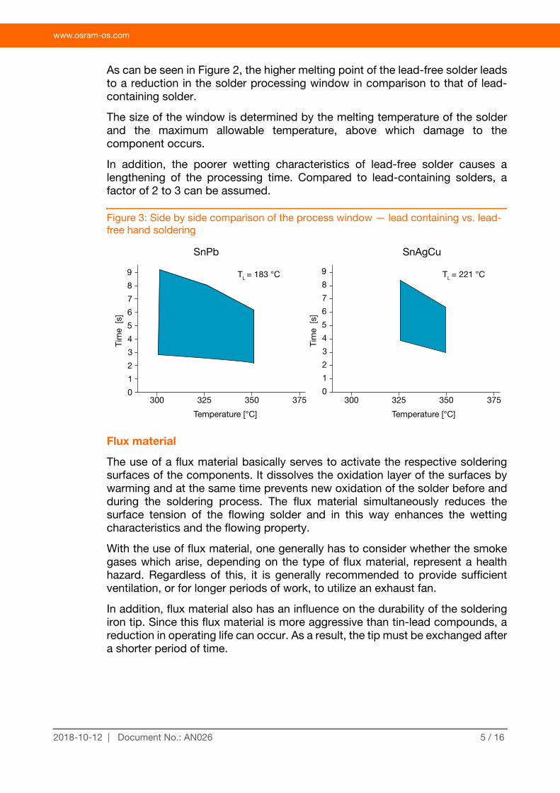
As can be seen in Figure 2, the higher melting point of the lead-free solder leadsto a reduction in the solder processing window in comparison to that of lead-containing solder.
The size of the window is determined by the melting temperature of the solderand the maximum allowable temperature, above which damage to thecomponent occurs.
In addition, the poorer wetting characteristics of lead-free solder causes alengthening of the processing time. Compared to lead-containing solders, afactor of 2 to 3 can be assumed.
Figure 3: Side by side comparison of the process window — lead containing vs. lead-free hand soldering
Flux material
The use of a flux material basically serves to activate the respective solderingsurfaces of the components. It dissolves the oxidation layer of the surfaces bywarming and at the same time prevents new oxidation of the solder before andduring the soldering process. The flux material simultaneously reduces thesurface tension of the flowing solder and in this way enhances the wettingcharacteristics and the flowing property.
With the use of flux material, one generally has to consider whether the smokegases which arise, depending on the type of flux material, represent a healthhazard. Regardless of this, it is generally recommended to provide sufficientventilation, or for longer periods of work, to utilize an exhaust fan.
In addition, flux material also has an influence on the durability of the solderingiron tip. Since this flux material is more aggressive than tin-lead compounds, areduction in operating life can occur. As a result, the tip must be exchanged aftera shorter period of time.
9
8
7
6
5
4
3
2
1
0300 325 350 375
Tim
e [s
]
SnPb
TL = 183 °C 9
8
7
6
5
4
3
2
1
0300 325 350 375
Tim
e [s
]
SnAgCu
TL = 221 °C
Temperature [°C]Temperature [°C]
5 / 162018-10-12 | Document No.: AN026
www.osram-os.com
Type of soldering iron
Many types of soldering irons are available. The main differences are the heatingpower and the precision of temperature regulation.
With older soldering iron models, the temperature measurement and regulationusually occurs at the internal heating element. Due to the distance from thesoldering tip, large deviations from the actual temperature of the soldering tip (upto 50 °C) can occur. Combined with higher melting temperatures of lead-freesolder, this increases the risk of overheating or can lead to temperature lossesduring the manual soldering process.
Better results can be achieved for lead-free solder with the help of modernsoldering stations which possess regulated heat management as well as internalprocess monitoring. With modern soldering irons, temperature regulation occursat the soldering tip rather than at the heating element. In addition, the solderingirons are equipped with sufficient heating power (> 80 W) and exhibit extremelyfast warming characteristics. This ensures that all solder joints are created withnearly the same temperature.
Soldering temperature
In general, it is recommended to use the lowest temperature possible,depending on the solder used. On the one hand, this prevents damage to heat-sensitive components and on the other the operating life of the soldering iron isextended.
With an increase in temperature, the wetting time for lead-free solder can indeedbe reduced, but this can damage certain types of components and reduce theoperating life of the soldering iron.
Since the melting point of lead-free solder is around 40 °C higher than themelting point of typical tin-lead compounds, the temperature of the soldering tipmust be set higher as a consequence.
In general, it is typical and also acceptable that the temperature of the solderingtip is set to be 50 °C higher than the melting point of the solder. However,soldering temperatures are often selected which are 100 °C higher than themelting temperature. This excess temperature is ultimately dependent on theheat capacity of the LED to be soldered, the extent of the solder joint and the sizeof the soldering tip.
D. Possible problem / risks
Prototyping
With manual soldering, the most common problems are damaging the LEDs orthe circuit board (base material, solder resist mask, pads etc.) and poor solderjoints. Soldering of larger LEDs with a higher heat binding potential causes thegreatest difficulty in most cases. An improvement can possibly be achieved withthe use of an additional heat source (heating pad, IR radiator, etc.).
6 / 162018-10-12 | Document No.: AN026
www.osram-os.com
Poor solder joints most often occur if the surfaces are not clean or are stronglyoxidized. With lead-free compounds, this is seen more often. One possibleremedy is the use of an aggressive flux material. However, this can lead toadditional problems. Since solder wire is produced with several types of flux,some of which are more corrosive than others, an initial test should be performedwith respect to its suitability. A further possibility is the use of an additional fluxmaterial for the components.
Rework
When reworking components already soldered with lead-free solder, it should benoted that not all alloys can be mixed together. Some combinations can lead tounreliable solder connections. Normally the same alloy as for to the formersoldering is used.
In case different alloys are used in parallel, it would be advantageous to mark orlabel the solder pads and possibly the components, in order to provideinformation about the solder used.
Since a higher temperature is required during rework due to a change in thecomposition of the material, it can happen that both the components and circuitboard can be damaged in the process. Careful, skilled work along with processand temperature monitoring are thus strongly recommended.
Furthermore, depending on the condition and storage time of the components tobe processed, a more aggressive flux material may possibly be required.
E. Basic rules for manual soldering
• A good heat contact between the soldering tip and the solder joint(component and PCB) must be created. This can only be achieved withflowing solder.
• The flux material should perform its effect at the appropriate locations andshould therefore flow freely to the locations to be soldered. This alsoenhances the heat transfer.
• The contact between the soldering iron and the location to be solderedshould only be maintained until the solder has freely flowed.
• Only as much solder as needed should be used. For stranded-wireconnections, the contour of the wires should remain visible.
• The LEDs must not be permitted to move during the solidification process.
Additional rules for lead-free soldering
• The temperature of the soldering tip must be raised in comparison to thatrequired for lead-containing solder (+ 25 °C to + 40 °C)
• The upper limit must not be increased, as this would result in delaminationof the circuit board or thermal damage to the components. For thesoldering procedure, this means that the processing window becomes
7 / 162018-10-12 | Document No.: AN026
www.osram-os.com
narrower.
• With lead-free solder, the flow behavior is poorer; the solder time increasesby 50 – 100 % in comparison to lead-containing solder.
• Exertion of pressure during soldering should be avoided so that thesoldering tip does become deformed or the components will damaged.
• Since lead-free solder is more aggressive, there is more wear and tear onthe soldering tip. The soldering stations should be switched off when not inuse or when no standby function is available.
• The use of fast heating soldering tips is preferable, since these are morequickly placed into operation.
• After the soldering, the tip should be cleaned and tin-plated.
F. Lead-free hand soldering process
In general, it is recommended to prepare and provide all necessary tools,materials and additional auxiliary tools before the soldering process.
This also means that the circuit board should be cleaned if necessary, in orderto remove oxidation or other impurities. Care should be taken that cleansingitself does not cause damage to the circuit board or circuit traces which couldinterfere or inhibit the wetting of the solder. In order to minimize or preventadditional effort, it is advantageous to populate new circuit boards directly aftermanufacture, or package them in a vacuum or inert gas for later processing.Contamination or progressive oxidation is thereby prevented.
In case of rework of already populated boards, this means that if necessary, theboards should be preheated in an appropriate oven, depending on storageconditions and time. Preheating serves to remove absorbed moisture andprevent the so-called “popcorn” effect with components. The duration andtemperature of the preheating procedure is individually determined, dependenton the components on the circuit board and the storage and environmentalconditions.
Tools and materials
As mentioned previously, lead-free solder places special demands andrequirements on the soldering equipment. Representative of equipmentavailable on the market, three appropriate and proven soldering stations arelisted here.
ERSA: i-CON Soldering Station & i-Tool Soldering Iron, 150 W
WELLER: WD2M Soldering Station, 160 W
METCAL: Soldering Station PS 800
All three systems were specially developed and optimized for lead-freesoldering. In comparison to older soldering stations for example, the solderingsystem from ERSA possesses precise temperature regulation at the soldering tip
8 / 162018-10-12 | Document No.: AN026
www.osram-os.com
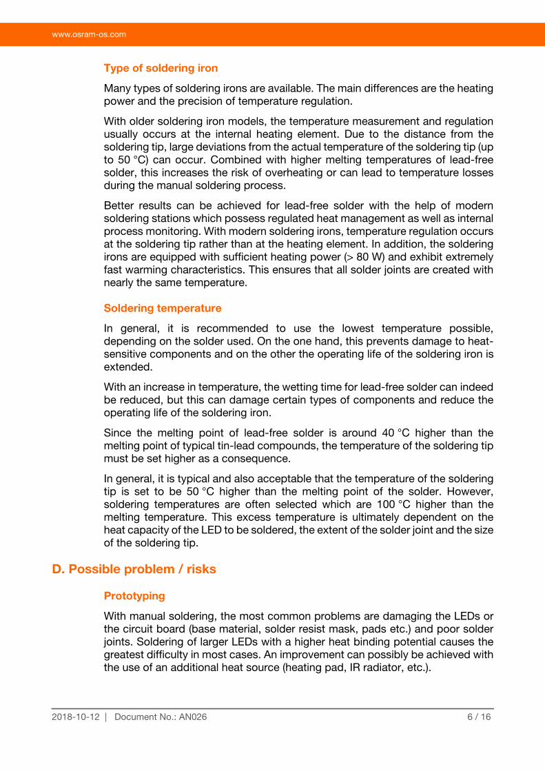
and extremely fast warm-up characteristics. In addition, it is equipped with aprocess window alarm and an automatic standby sensor as well as other user-friendly functions. Other systems are similarly equipped. For the soldering ironsmentioned above, several different soldering tips are available which can bespecifically adapted and optimized for the component.
Figure 4: Tip selection — correct geometry for each application
As auxiliary tools, various sizes of tweezers are recommended for better handlingof LEDs along with a desoldering braid or pump for removal of solder pasteduring repair work. In addition, the use of a so-called “third hand”, an adjustablefixture for holding the circuit board, and a magnifying glass can also be helpful.In general, ESD protection should additionally be provided for the componentsand/or the populated circuit board. This can be achieved with a groundingarmband, grounded table or support, etc. When soldering, the use of solder wirewith flux core is preferable. This is available in several diameters and provides asufficient amount of flux in most cases.
As an example, solder wire from EDSYN consisting of SnAgCu with NO-CLEANflux as per F SW34 can be used. For soldering of LEDs, particularly for miniaturecomponents, a diameter of 0.35 mm is sufficient. Depending on the size of theLED or component to be soldered, heavier solder wire can be used.
With the use of solder wire with a flux core, the solder and flux can spray out dueto the very quick warming of the solder.The flux tends to carbonize in the processand the desired effectiveness is reduced. An improvement can be achieved witha V-formed notch in the solder wire, permitting more effective use of the fluxmaterial.
General solder technique / procedure
The soldering technique and correct procedure is basically not different from theold technique for lead-containing solder.
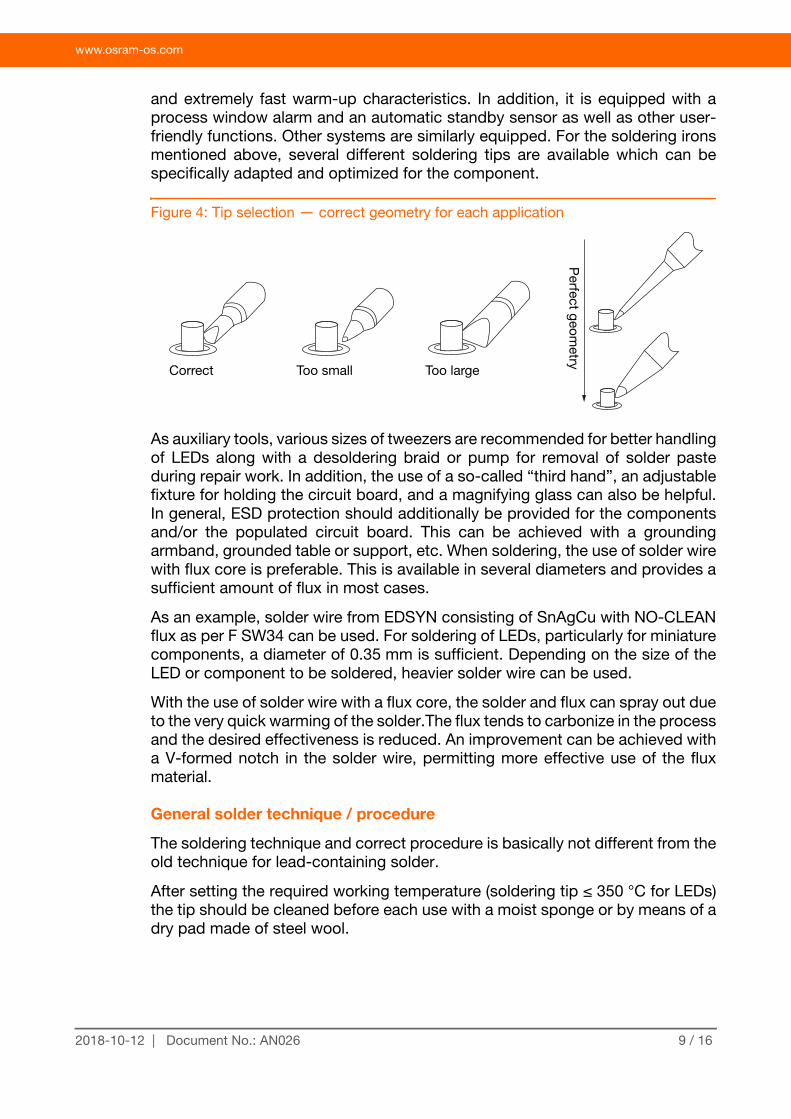
After setting the required working temperature (soldering tip ≤ 350 °C for LEDs)the tip should be cleaned before each use with a moist sponge or by means of adry pad made of steel wool.
Correct Too small Too large
Perfect geom
etry
9 / 162018-10-12 | Document No.: AN026
www.osram-os.com
Figure 5: Example of moist sponge for cleaning soldering tips
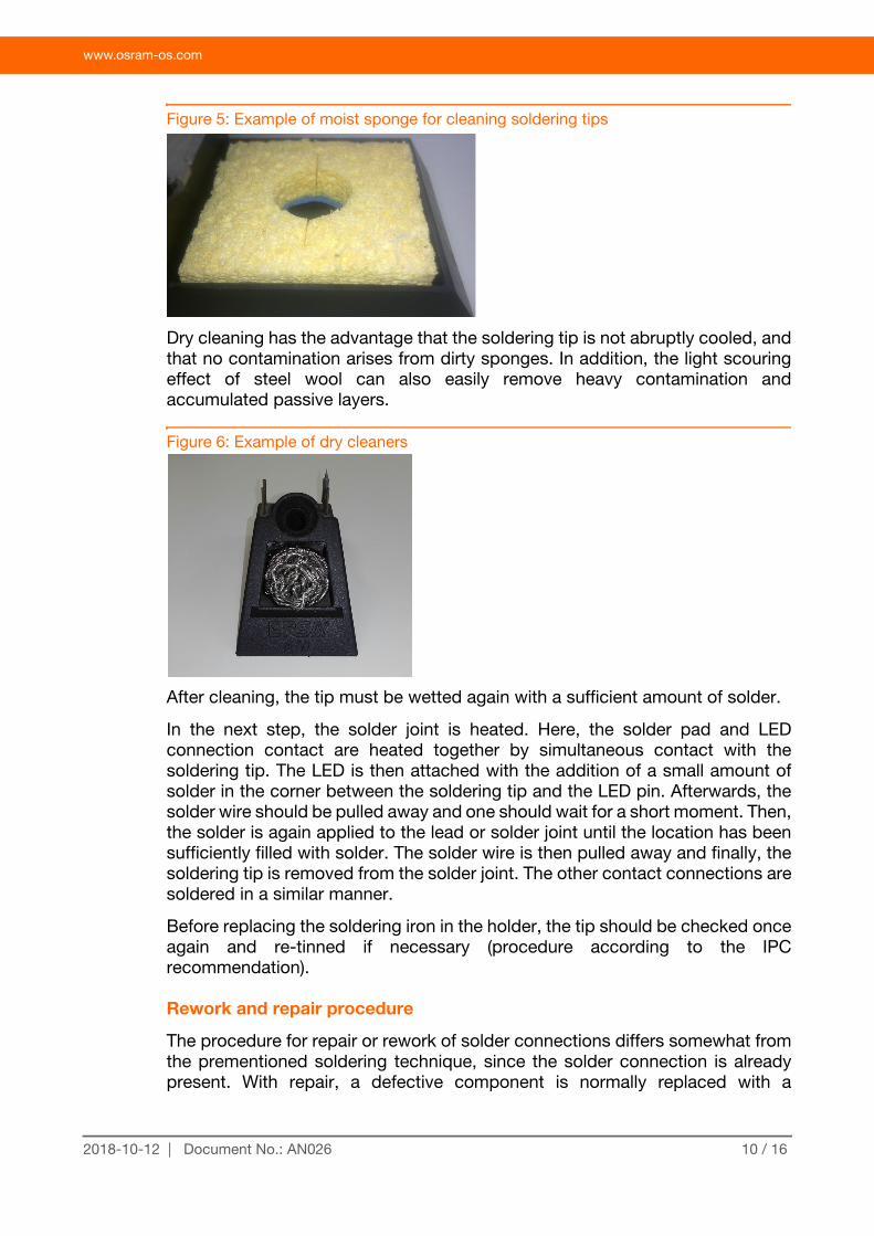
Dry cleaning has the advantage that the soldering tip is not abruptly cooled, andthat no contamination arises from dirty sponges. In addition, the light scouringeffect of steel wool can also easily remove heavy contamination andaccumulated passive layers.
Figure 6: Example of dry cleaners
After cleaning, the tip must be wetted again with a sufficient amount of solder.
In the next step, the solder joint is heated. Here, the solder pad and LEDconnection contact are heated together by simultaneous contact with thesoldering tip. The LED is then attached with the addition of a small amount ofsolder in the corner between the soldering tip and the LED pin. Afterwards, thesolder wire should be pulled away and one should wait for a short moment. Then,the solder is again applied to the lead or solder joint until the location has beensufficiently filled with solder. The solder wire is then pulled away and finally, thesoldering tip is removed from the solder joint. The other contact connections aresoldered in a similar manner.
Before replacing the soldering iron in the holder, the tip should be checked onceagain and re-tinned if necessary (procedure according to the IPCrecommendation).
Rework and repair procedure
The procedure for repair or rework of solder connections differs somewhat fromthe prementioned soldering technique, since the solder connection is alreadypresent. With repair, a defective component is normally replaced with a
10 / 162018-10-12 | Document No.: AN026
www.osram-os.com
functioning part. The existing solder connection must be melted and the solderremoved by means of a desoldering braid or a pump. With rework, however,individual solder joints are reworked because they are possibly damaged or notsufficiently formed. Here, it is also generally true that the soldering iron tip shouldbe cleaned and wetted with solder before use.
1. Heat the solder connections until the solder completely meltsIn general, the soldering iron should be held at the connection location withthe largest amount of solder. In order to achieve a good heat transfer, thetip should be simultaneously held against the solder pad and theconnection contact of the component.
2. Remove the liquid solder by means of a desoldering braid or a pump (repair)
3. Apply appropriate solder if necessary (rework)The solder wire is applied to the surface of the melted solder so that thesolder is melted there instead of at the soldering tip. In order to preventdamage to the component of the circuit board material, a maximum contacttime of 3 seconds should not be exceeded.
4. Solidification of the solder connectionAfter the soldering tip is removed, the connection solidifies again after a fewseconds and other leads of the component can be soldered.
5. Cleaning the solder jointsIn case cleaning is required, it is recommended to eliminate the flux residueas soon as possible. As a rule, dried residue adheres more tenaciously andcan only be removed with greater difficulty and by more aggressive means.
Visual assessment of the solder joints
After soldering, a visual assessment should be performed in any case, withrespect to the appearance and quality of the connection. The person carrying outthis assessment should be trained in this regard and have sufficient experience.For a confident and reliable assessment, criteria according to IPC-Standard(IPC-A-610) are drawn upon worldwide. A few excerpts include:
• The solder joint should be uniform and smooth in appearance (shiny is notrequired).
• The solder should taper off from the inserted parts (small contact angle).
• The surface of the solder joint should be unbroken.
• The contours of the soldered parts should be recognizable in the solderjoint.
• The solder joint must contain sufficient solder.
Additional information and exact details can be obtained from the IPC Standard.
11 / 162018-10-12 | Document No.: AN026
www.osram-os.com
Cleaning
In most cases, final cleaning is only necessary to remove any flux residue whichmay be present. Essentially, other residues or contamination should not bepresent.
Often, various cleansing solutions or cleaning by means of an ultrasonic bath isrecommended by solder manufacturers. With the presence of LEDs, however,this is only conditionally or not at all possible.
In principle, isopropyl alcohol (IPA) can be used, since this is also suitable andapproved for cleaning LEDs from OSRAM Opto Semiconductors.
If other cleansing solutions are applied, their suitability should be testedbeforehand, particularly if there is associated damage to the LED. Because ofworldwide regulations, cleansers such as FREON or other compoundscontaining chloroflurocarbons (CFCs) should not be used.
Cleaning by means of an ultrasonic bath is not recommended for LEDs. Thereason for this is that the influence on the LEDs is dependent on the ultrasonicpower, the duration of treatment and the cleansing solution used. If ultrasoniccleaning cannot be avoided, it must first be determined whether the LEDs will bedamaged in the process.
In the best and ideal case, cleaning is not required if solder with so-called NO-CLEAN flux is used. With this type of flux material, it is not necessary to removethe remaining residue from the connections or circuit board in order to guaranteereliability.
It is simpler as well to resort to water-soluble flux material. Meanwhile, there aresystems which also permit better wetting of lead-free materials without nitrogen.
Important LED-specific points
Since LED packages predominantly consist of plastic and ceramic, the directcontact with a hot soldering tip can often lead to damage of the device.
This applies exceptionally to the plastic optics of the LEDs. In addition, it shouldbe noted that with higher soldering tip temperatures, heat is transferred faster tothe package via the connection contacts.The prescribed solder times should notbe exceeded, since this can otherwise damage the component. It should also benoted that with the various packaging types, the size and form of the connectioncontacts vary as well. For optimal soldering results, it is recommended to useindividually adapted soldering tips. If a soldering tip is too large or wide forminiature components, for example, this can lead to overheating and thusdamages to the component package. If a small, narrow tip is used for largercontacts, however, insufficient heat is available for a good solder connection.
Particular experience combined with special care and higher demands arerequired for the processing of LED with high power housings. The reason for thisis the heat slug integrated in the package base. For optimal heat transfer, thismust be affixed or soldered to the circuit board. Soldering of the heat slug itselfcan only occur with the help of solder paste and an additional heating plate.
12 / 162018-10-12 | Document No.: AN026
www.osram-os.com
Since the heat slug is embedded in the package base, direct contact with thesoldering iron is not possible; for this reason, rework at the heat slug cannot becarried out.
Generally it is advisable to use an additional heating plate for lead-free solderingof LEDs, especially if an insulated metal substrate is utilized.
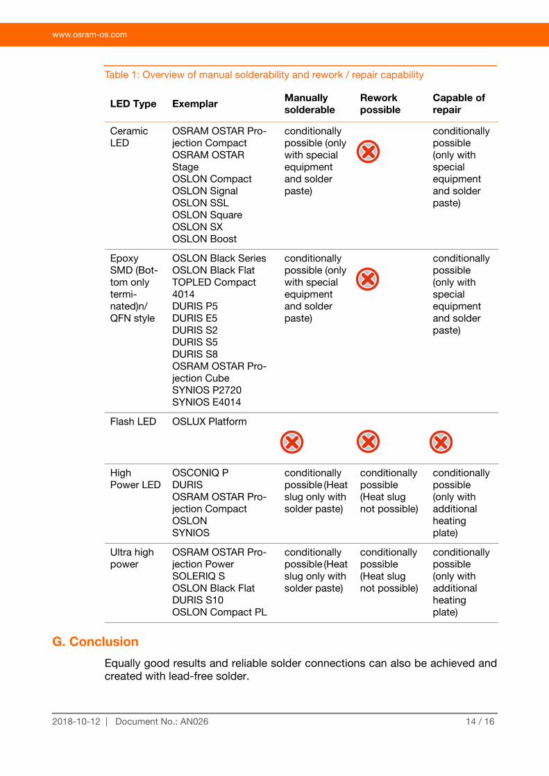
In the following, Table 1 provides an overview of the manual solderability ofvarious LED types from OSRAM Opto Semiconductors as well as their repair andrework capability.
Table 1: Overview of manual solderability and rework / repair capability
LED Type Exemplar Manually solderable
Rework possible
Capable of repair
Radial or Through-hole LED
T1T1 3/4Sidelooker
Miniature Compo-nents
Smart LEDCHPILEDFIREFLY 0402
Mini Top Locker
Mini TOPLEDTOPLED E1608FIREFLY E1608Point LED
Side Looker
FIREFLY 0402Micro SIDELEDSIDELED
Top Looker
TOPLEDTOPLED with lensTOPLED BlackTOPLED Black Sur-faceTOPLED E3014Multi TOPLEDMULTILEDCHIPLEDMulti CHIPLEDDISPLIXDURIS EDURIS PDURIS S
Mid power LED
Adv. Power TOPLED
13 / 162018-10-12 | Document No.: AN026
www.osram-os.com
G. Conclusion
Equally good results and reliable solder connections can also be achieved andcreated with lead-free solder.
conditionally possible (Heat slug only with solder paste)
conditionally possible (Heat slug not possible)
conditionally possible (only with additional heating plate)
Ultra high power
OSRAM OSTAR Pro-jection PowerSOLERIQ SOSLON Black FlatDURIS S10OSLON Compact PL
conditionally possible (Heat slug only with solder paste)
conditionally possible (Heat slug not possible)
conditionally possible (only with additional heating plate)
Table 1: Overview of manual solderability and rework / repair capability
LED Type Exemplar Manually solderable
Rework possible
Capable of repair
14 / 162018-10-12 | Document No.: AN026
www.osram-os.com
The prerequisite for this, however, is that one thoroughly understands theproperties and differences of the new solder and also considers thecorresponding process from a technical standpoint. In addition, with manualsoldering, it is generally recommended to take into account the specific featuresof the component or LED such as the package form, lead size, etc. when definingthe process window.
Basically, manual soldering with lead-free solder is not much more difficult thansoldering with lead-containing solder, so long as work is performed withappropriate equipment, qualified employees and the fundamental ground rulesare strictly maintained.
15 / 162018-10-12 | Document No.: AN026
www.osram-os.com
Don't forget: LED Light for you is your place tobe whenever you are looking for information orworldwide partners for your LED Lightingproject.
www.ledlightforyou.com
ABOUT OSRAM OPTO SEMICONDUCTORS
OSRAM, Munich, Germany is one of the two leading light manufacturers in the world. Its subsidiary, OSRAMOpto Semiconductors GmbH in Regensburg (Germany), offers its customers solutions based on semiconduc-tor technology for lighting, sensor and visualization applications. OSRAM Opto Semiconductors has produc-tion sites in Regensburg (Germany), Penang (Malaysia) and Wuxi (China). Its headquarters for North Americais in Sunnyvale (USA), and for Asia in Hong Kong. OSRAM Opto Semiconductors also has sales offices th-roughout the world. For more information go to www.osram-os.com.
DISCLAIMER
PLEASE CAREFULLY READ THE BELOW TERMS AND CONDITIONS BEFORE USING THE INFORMA-TION SHOWN HEREIN. IF YOU DO NOT AGREE WITH ANY OF THESE TERMS AND CONDITIONS, DONOT USE THE INFORMATION.
The information provided in this general information document was formulated using the utmost care; howe-ver, it is provided by OSRAM Opto Semiconductors GmbH on an “as is” basis. Thus, OSRAM Opto Semicon-ductors GmbH does not expressly or implicitly assume any warranty or liability whatsoever in relation to thisinformation, including – but not limited to – warranties for correctness, completeness, marketability, fitnessfor any specific purpose, title, or non-infringement of rights. In no event shall OSRAM Opto SemiconductorsGmbH be liable – regardless of the legal theory – for any direct, indirect, special, incidental, exemplary, con-sequential, or punitive damages arising from the use of this information. This limitation shall apply even ifOSRAM Opto Semiconductors GmbH has been advised of possible damages. As some jurisdictions do notallow the exclusion of certain warranties or limitations of liabilities, the above limitations and exclusions mightnot apply. In such cases, the liability of OSRAM Opto Semiconductors GmbH is limited to the greatest extentpermitted in law.
OSRAM Opto Semiconductors GmbH may change the provided information at any time without giving noticeto users and is not obliged to provide any maintenance or support related to the provided information. Theprovided information is based on special conditions, which means that the possibility of changes cannot beprecluded.
Any rights not expressly granted herein are reserved. Other than the right to use the information provided inthis document, no other rights are granted nor shall any obligations requiring the granting of further rights beinferred. Any and all rights and licenses regarding patents and patent applications are expressly excluded.
It is prohibited to reproduce, transfer, distribute, or store all or part of the content of this document in any formwithout the prior written permission of OSRAM Opto Semiconductors GmbH unless required to do so in ac-cordance with applicable law.