2014 Microchip Technology Inc. DS00001785A-page 1 INTRODUCTION In many microcontroller-based applications, the microcontroller is subjected to various types of electromagnetic noise. Electrical noises may cause undesirable behavior on the application. Two of these types of noise events are referred to as Electrostatic Discharge (ESD) and Electrical Overstress (EOS). This application note discusses these two types of events, what causes them and how to minimize the impact of them on the application. WHAT IS ESD? The Electrostatic Discharge (ESD) is the most common phenomena of Electro-Magnetic Compliance (EMC). The word, electrostatic, indicates static electricity accu- mulated by specific materials that come into contact with one another, such as rubbing your feet on a wool carpet. The electric spark that is sometimes experienced when touching metal, or a car, is the phenomenon of Electro- static Discharge (ESD). The amount of electric discharge depends upon the material and environment, including humidity. ESD discharge not only happens when a human comes in contact with a statically charged material. Machines and furniture, such as lab tables, can also accumulate static electricity, and discharge when electrical components come in contact with them. Specification IEC 61000-4-6 defines the static electric- ity accumulated by humans and machines. The models are called: “Human Body Model (HBM)” and “Machine Model (MM)”. Figure 1 below shows the ESD voltages as defined by the IEC standards. FIGURE 1: ESD VOLTAGES As described in Figure 1, the accumulated static electric- ity depends on the relative humidity of the environment. When the humidity is lower, the accumulated static electricity is higher. Table 1 describes typical voltages with very common materials used in daily life with respect to the relative humidity. TABLE 1: COMMON STATIC VOLTAGES Authors: Padmaraja Yedamale Enrique Aleman Microchip Technology Inc. Static Voltages as a Function of Relative Humidity (RH) 20% RH (kV) 80% RH (kV) Walking across a vinyl floor 12 0.25 Walking across a synthetic carpet 35 1.5 Arising from a foam cushion 18 1.5 Picking up a polyethylene bag 20 0.6 Sliding a styrene box on a carpet 18 1.5 Removing mylar tape from a PC board 12 1.5 Shrinkable film on a PC board 16 3.0 Triggering a vacuum solder remover 8 1.0 Aerosol circuit freeze spray 15 5.0 15 13 9 5 1 15 35 40 80 100 Relative Humidity % } e.g., Office Room without Humidity Control (Winter Time) Synthetic Wool Anti-Static Peak Voltage (kV) AN1785 ESD and EOS Causes, Differences and Prevention
Transcript
AN1785ESD and EOS Causes, Differences and Prevention
INTRODUCTIONIn many microcontroller-based applications, themicrocontroller is subjected to various types ofelectromagnetic noise. Electrical noises may causeundesirable behavior on the application. Two of thesetypes of noise events are referred to as ElectrostaticDischarge (ESD) and Electrical Overstress (EOS).This application note discusses these two types ofevents, what causes them and how to minimize theimpact of them on the application.
WHAT IS ESD?The Electrostatic Discharge (ESD) is the most commonphenomena of Electro-Magnetic Compliance (EMC).The word, electrostatic, indicates static electricity accu-mulated by specific materials that come into contact withone another, such as rubbing your feet on a wool carpet.The electric spark that is sometimes experienced whentouching metal, or a car, is the phenomenon of Electro-static Discharge (ESD). The amount of electric dischargedepends upon the material and environment, includinghumidity.
ESD discharge not only happens when a humancomes in contact with a statically charged material.Machines and furniture, such as lab tables, can alsoaccumulate static electricity, and discharge whenelectrical components come in contact with them.
Specification IEC 61000-4-6 defines the static electric-ity accumulated by humans and machines. The modelsare called: “Human Body Model (HBM)” and “MachineModel (MM)”.
Figure 1 below shows the ESD voltages as defined bythe IEC standards.
FIGURE 1: ESD VOLTAGES
As described in Figure 1, the accumulated static electric-ity depends on the relative humidity of the environment.When the humidity is lower, the accumulated staticelectricity is higher. Table 1 describes typical voltageswith very common materials used in daily life withrespect to the relative humidity.
TABLE 1: COMMON STATIC VOLTAGES
Authors: Padmaraja YedamaleEnrique AlemanMicrochip Technology Inc.
Static Voltages as a Function ofRelative Humidity (RH)
20% RH(kV)
80% RH(kV)
Walking across a vinyl floor 12 0.25Walking across a synthetic carpet 35 1.5Arising from a foam cushion 18 1.5Picking up a polyethylene bag 20 0.6Sliding a styrene box on a carpet 18 1.5Removing mylar tape from a PC board 12 1.5Shrinkable film on a PC board 16 3.0Triggering a vacuum solder remover 8 1.0Aerosol circuit freeze spray 15 5.0
15
13
9
5
115 35 40 80 100
Relative Humidity %
} e.g., Office Room withoutHumidity Control (Winter Time)
Synthetic
Wool
Anti-Static
PeakVoltage
(kV)
2014 Microchip Technology Inc. DS00001785A-page 1
AN1785
ESD testing is done at various levels in a product cycle,such as at the component level (for example, Microchip’sMCU), at the board level (such as control board) and atthe end equipment level (such as a washing machine).
From the standpoint of Microchip’s products, there areprotection circuits built into the chip to avoid any dam-age that can be caused by typical levels of ESD. As perthe quality process, all Microchip devices are testedbased on the following standards:
• ANSI/ESDA/JEDEC JS-001-2012 for Electrostatic Discharge Sensitivity Testing, Human Body Model (HBM) – Component Level
• JESD22-A115 for Electrostatic Discharge (ESD) Sensitivity Testing, Machine Model (MM)
• ANSI/ESD S5.2-2009 for Electrostatic Discharge Sensitivity Testing, Machine Model (MM) – Component Level
Microchip publishes the “Quality Handbook” (DS00169)that can be downloaded from Microchip’s website byclicking on this link: http://www.microchip.com/quality
After the chip is assembled on a PCB, a systemdesigner will test the application for ESD sensitivity atthe PCB level. Typically, at this level, the connectorsand the cables have a conducted discharge applied tothem.
An end equipment manufacturer, such as an appliancemanufacturer, will test the end equipment for ESD sen-sitivity based on the first point of contact. The first pointof contact is defined as the point of contact for the enduser or assembly equipment. For example, on a refrig-erator, the point of contact is the door handle ordispenser keys; on a washing machine, it could be thekeys of a display or control knobs. An example of anESD immunity testing specification for PCBs and endproducts can be found in the international standard,IEC-61000-4-2.
In general, to minimize the effects of ESD on PCBs andend products, the design should shunt the ESD energyto ground in the most effective way possible.
WHAT IS EOS?In a semiconductor environment, Electrical Overstress(EOS) is a term used to describe the phenomenon thatmay occur when an electronic device is subjected to acurrent or voltage that is beyond the specification limitsof the device. The Electrical Overstress may result inthermal damage to the entire device or a portion of thedevice. The thermal damage is the result of the exces-sive heat generated during the EOS event. When adevice is subjected to high voltage or current, resistiveheating in the connections within the device generatesexcessive temperatures. Typically, the excessive heat islocalized around the area where the electrical stress isexerted. This results in damage to the device, and mostof the time, this damage is visible to the naked eye.
EOS can be the result of a single non-recurring event orthe result of ongoing periodic, or non-periodic events. AnEOS event can be a momentary event, lasting only milli-seconds, or can last as long as the conditions persist.After the EOS energy is dissipated, the device may bepermanently damaged and may become non-functionalor partially functional.
Possible Causes of EOSThe following is a list of issues that can cause EOS:
1. Power supply voltage surge beyond the absolutemaximum voltage range.
2. Switching circuits on the board may cause high-voltage spikes internal to the board, propagatedto other devices on the board.
3. External connections, such as capacitive chargeon an external cable, antenna pick-up of externalswitching noise and inductive loads can createvoltage spikes.
4. Excessive noise on the ground plane due topoor grounding.
5. I/O switching creating voltage overshoots orundershoots.
6. EMI (Electromagnetic Interference) due to poorshielding in an electrically noisy environment.
7. Improper power-up sequences can applyunintended voltage levels or polarities to thedevice.
8. ESD events that cause damage, or weaken thedevice, making it more susceptible to futureEOS events.
9. Latch-up events may result in EOS damage ifthe current is high or if it persists for an extendedperiod of time.
DS00001785A-page 2 2014 Microchip Technology Inc.
AN1785
ESD VERSUS EOSThe primary difference between ESD and EOS eventsis their time duration. ESD events are generallybetween 500V and 8000V, and last for less than300 nS. During an ESD event, the peak current canreach many amps of current, but because the event isso short, a well designed ESD protection circuit canshunt this energy to ground which causes no damage.While voltage and current levels can be similar, an EOSevent has a much longer duration, typically from 1 mSto many minutes.
Electrical failure in an application may show one ormore of the following symptoms:
1. Excess supply current.2. Low resistance between the supply voltage and
ground.3. Shorted input or output pins to either the supply
voltage, or ground.4. Open connections to one or multiple pins – I/O,
supply voltage or ground.5. Functional failure due to internal damage to the
The difference between the observed symptoms ofEOS and ESD are often not clear, and in some cases,a wrong diagnosis can lead to an ineffective solution.The following section contains some guidelines thatmay help identify an EOS failure versus an ESD failure,along with photos and diagrams that illustrate thetypical damage seen for each type of failure.
The goal of the “Characteristics of an ESD Failure”section is to help in understanding the differences, soproper feedback can be provided to achieve timelysolutions to the failures.
2014 Microchip Technology Inc. DS00001785A-page 3
AN1785
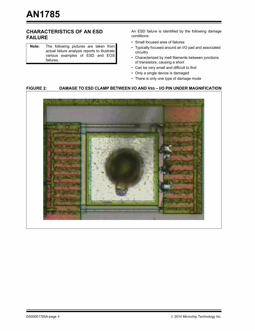
CHARACTERISTICS OF AN ESD FAILURE
An ESD failure is identified by the following damageconditions:
• Small focused area of failures• Typically focused around an I/O pad and associated
circuitry• Characterized by melt filaments between junctions
of transistors, causing a short• Can be very small and difficult to find• Only a single device is damaged• There is only one type of damage mode
FIGURE 2: DAMAGE TO ESD CLAMP BETWEEN I/O AND VSS – I/O PIN UNDER MAGNIFICATION
Note: The following pictures are taken fromactual failure analysis reports to illustratevarious examples of ESD and EOSfailures.
DS00001785A-page 4 2014 Microchip Technology Inc.
AN1785
Figure 3 shows ESD damage to gate oxide, indicativeof a charged device ESD failure, an input without anyprotection or where there is no secondary protection.
FIGURE 3: ESD DAMAGE TO GATE OXIDE – IMAGE OF A DEPROCESSED CHIP LAYER
2014 Microchip Technology Inc. DS00001785A-page 5
AN1785
FIGURE 4: ESD DAMAGE TO METAL INTERCONNECTS
FIGURE 5: ESD DAMAGE TO SILICON JUNCTION
DS00001785A-page 6 2014 Microchip Technology Inc.
AN1785
Figure 6 shows ESD damage that is so severe it almostresembles EOS. This could be a condition where anEOS event further damaged the circuit which wasalready weakened by ESD.
FIGURE 6: SEVERE ESD DAMAGE
2014 Microchip Technology Inc. DS00001785A-page 7
AN1785
CHARACTERISTICS OF AN EOS FAILUREAn EOS failure is identified by the following damageconditions:
• Large areas of damage are seen• Characterized by a large amount of melted metal• Can be localized to an I/O pad or internal to the die
in the case of an EOS event on a supply pin• Damage can encompass many devices• Can have many different simultaneous damage
types
Other causes of EOS are:
• Output currents which exceed device maximums (short circuits or low-impedance loads)
• I/O pins which spike above VDD or below VSS
• VDD which exceeds the VDD maximum specification
EOS is a long-term event and is usually caused by useror test errors (e.g., the part may have been put in thesocket backwards). The most common cause of EOSis overvoltage on either the I/O pin or the supply pin.
Visual Damage Due to EOSWhen failure analysis is done on a device, typically,EOS damage can be seen as visual damage on thedevice using only an optical microscope. This damageis the result of the high temperature experienced duringthe EOS event. External damage to the package may also be seen asa result of EOS stress and is characterized by:1. Cracked package.2. Visible bulge in mold compound.3. Physical hole in mold compound.4. Burnt/discolored mold compound.The sample may be damaged more than listed above,but a careful analysis, by removing the capsulatingmaterial from the part, may show the following internaldamage due to excessive temperature:1. Package/die delamination from excessive heat.2. Melted or burnt metal layers.3. Carbonized mold compound.4. Discoloration to metal lines.5. Melted or vaporized bond wires.
Examples of EOS FailureThe following figures illustrate the different examples ofEOS failure.
FIGURE 7: MOLD COMPOUND CARBONIZATION DUE TO EOS EXCESSIVE HEAT
DS00001785A-page 8 2014 Microchip Technology Inc.
AN1785
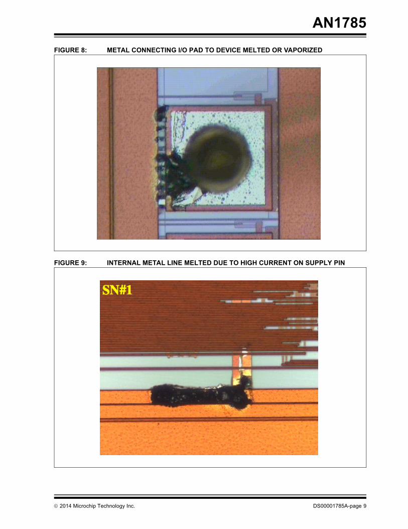
FIGURE 8: METAL CONNECTING I/O PAD TO DEVICE MELTED OR VAPORIZED
FIGURE 9: INTERNAL METAL LINE MELTED DUE TO HIGH CURRENT ON SUPPLY PIN
2014 Microchip Technology Inc. DS00001785A-page 9
AN1785
FIGURE 10: MELTED AND DISCOLORED METAL IN COMBINATION WITH CARBONIZED MOLD
COMPOUND
FIGURE 11: CARBONIZED MOLD COMPOUND, MELTED AND DISCOLORED METAL
DS00001785A-page 10 2014 Microchip Technology Inc.
AN1785
FIGURE 12: EOS DAMAGE TO PACKAGING
2014 Microchip Technology Inc. DS00001785A-page 11
AN1785
ESD AND EOS TESTING
Device Robustness DesignMicrochip devices are designed with protection cir-cuitry to avoid damage due to an ESD event during thehandling and assembly process. As part of the qualityprocess, all Microchip devices are tested against twoJEDEC standards, as described below.
Device TestingAll of the Microchip Technology devices are designedto withstand ESD testing according to the followingstandards:
• ANSI/ESDA/JEDEC JS-001-2012 for Electrostatic Discharge Sensitivity Testing, Human Body Model (HBM) – Component Level
• JESD22-A115 for Electrostatic Discharge (ESD) Sensitivity Testing, Machine Model (MM)
Other ESD standards used for reference:
• MIL-STD 883 Notice 8 Method 3015.7 “Military Standard for Test Methods and Procedures Microelectronics: ESD Sensitivity Classification”
• ANSI/ESD S5.3.1-2009 for Electrostatic Discharge Sensitivity Testing, Charged Device Model (CDM) – Component Level
• JESD22-C101 “Field-Induced Charged Device Model Test Method for Electrostatic Discharge Withstand Thresholds of Microelectronic Components”
• ANSI/ESD S5.2-2009 for Electrostatic Discharge Sensitivity Testing, Machine Model (MM) – Component Level
• AEC - Q100-002 for Human Body Model Electrostatic Discharge Test
• AEC - Q100-003 for Machine Model Electrostatic Discharge Test
• AEC - Q100-011 for Charged Device Model (CDM) Electrostatic Discharge Test
Additionally, latch-up sensitivity is tested according toJESD-78, and is performed on sample units with aminimum stress current of ±100 mA and an overvoltageof 1.5 * VMAX.
MINIMUM GUIDELINES2000V – HBM Sample: 12 (3 per voltage level)200V – MM Sample: 12 (3 per voltage level)500V – (corner pins: 750V) CDM Sample: 5
Human Body Model (HBM)The Human Body Model (HBM) is the most widely usedand quoted model for ESD testing.
The HBM simulates a human body dischargingaccumulated static charge through a grounded device.
FIGURE 13: HUMAN BODY MODEL (HBM)
Human Body Model
Grounded Surface
DS00001785A-page 12 2014 Microchip Technology Inc.
AN1785
The graph in Figure 14 shows the characteristics of theHBM test waveform. The Human Body Model has apeak of 1.2 to 1.3 amps for a 2 kV test. The rise time is2-10 ns, with the waveform decaying to 50% by 150 ns.The entire cycle is 500 ns.
FIGURE 14: HBM TEST WAVEFORM GRAPH CHARACTERISTICS
2014 Microchip Technology Inc. DS00001785A-page 13
AN1785
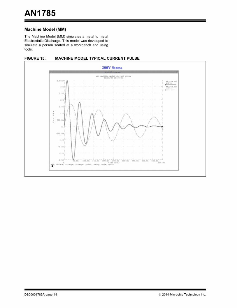
Machine Model (MM)The Machine Model (MM) simulates a metal to metalElectrostatic Discharge. This model was developed tosimulate a person seated at a workbench and usingtools.
FIGURE 15: MACHINE MODEL TYPICAL CURRENT PULSE
DS00001785A-page 14 2014 Microchip Technology Inc.
AN1785
The Machine Model uses ‘0 Ohms’ (see Figure 16) inthe test setup, the discharge current exhibits LC tankbehavior. Rise time is between 5 and 15 ns. The wave-form duration, peak and rise time are dependent on theparasitic inductance and capacitance in the DUT.
Both the Human Body and Machine Models are thesame test with different values for the test setup. Thebasic test circuit setup is detailed below.
FIGURE 16: BASIC TEST CIRCUIT SETUP
In the above circuit, R1 is the body resistance set tomimic the resistance of a human body or the toolsbeing used to handle the device.
Cc is the body capacitance set to mimic the total capacityof the human body. In a Machine Model, the capacitanceis higher since the person is seated.
CsL1
V+
Cc Ct
R1
Rt
Cc = Capacitance of Human Body/MachineHBM = 100 pFMM = 200 pF
L1 = Parasitic Line InductanceR1 = Source Resistance:
2014 Microchip Technology Inc. DS00001785A-page 15
AN1785
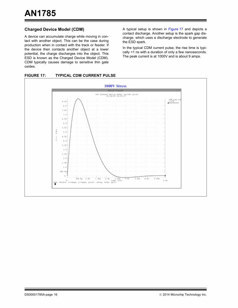
Charged Device Model (CDM)A device can accumulate charge while moving in con-tact with another object. This can be the case duringproduction when in contact with the track or feeder. Ifthe device then contacts another object at a lowerpotential, the charge discharges into the object. ThisESD is known as the Charged Device Model (CDM).CDM typically causes damage to sensitive thin gateoxides.
A typical setup is shown in Figure 17 and depicts acontact discharge. Another setup is the spark gap dis-charge, which uses a discharge electrode to generatethe ESD spark.
In the typical CDM current pulse, the rise time is typi-cally <1 ns with a duration of only a few nanoseconds.The peak current is at 1000V and is about 9 amps.
FIGURE 17: TYPICAL CDM CURRENT PULSE
DS00001785A-page 16 2014 Microchip Technology Inc.
AN1785
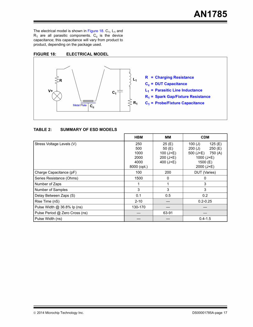
The electrical model is shown in Figure 18. C1, L1 andR1 are all parasitic components. Cc is the devicecapacitance; this capacitance will vary from product toproduct, depending on the package used.
FIGURE 18: ELECTRICAL MODEL
TABLE 2: SUMMARY OF ESD MODELS
L1
V+ C1
R1
R = Charging ResistanceCc = DUT CapacitanceL1 = Parasitic Line InductanceR1 = Spark Gap/Fixture ResistanceC1 = Probe/Fixture Capacitance
CcMetal Plate
R
HBM MM CDM
Stress Voltage Levels (V) 250500
100020004000
8000 (opt.)
25 (E)50 (E)
100 (J+E)200 (J+E)400 (J+E)
100 (J) 125 (E)200 (J) 250 (E)500 (J+E) 750 (A)
1000 (J+E)1500 (E)
2000 (J+E)Charge Capacitance (pF) 100 200 DUT (Varies)Series Resistance (Ohms) 1500 0 0Number of Zaps 1 1 3Number of Samples 3 3 3Delay Between Zaps (S) 0.1 0.5 0.2Rise Time (nS) 2-10 — 0.2-0.25Pulse Width @ 36.8% Ip (ns) 130-170 — —Pulse Period @ Zero Cross (ns) — 63-91 —Pulse Width (ns) — — 0.4-1.5
2014 Microchip Technology Inc. DS00001785A-page 17
AN1785
ESD CONTROL MECHANISMSElectrostatic Discharges can come from a variety ofsources. The traditional ESD pulse is caused by a body ata very high potential coming into contact, or near contact,with a grounded object. This could be a human body, apiece of electrical equipment or even a piece of furniture.
In a dry environment, where static dissipation is low, ahuman body can develop tens of thousands of volts ofpotential. Incorrectly placed ionizers, meant to improvestatic dissipation, can build large potentials on office orlaboratory furniture. Any person touching such a piece offurniture might feel a shock. Any devices being placedon a table with a large potential can suffer damage.
Personnel Grounding DevicesThe potential for ESD damage at assembly can beavoided by careful personnel grounding procedures.Ground straps for manual handling of devices is essen-tial. Other procedures include grounded tables and worksurfaces with anti-static surfaces, such as specificallydesigned plastic mats.
In addition, static dissipative garments can help drainany charge assembly personnel may accumulate.
A Faraday cage can be used to protect devices on theboard. The devices can be microprobed in the Faradaycage room and then stored in the cage room.
An ESD gun can be unintentionally used to createfailures. Check these into proper locations if applicable.
ESD PackagingProtective material packaging techniques are essentialto prevent any ESD damage. Packaging can be in theform of bags, package filler, magazines, boxes, carri-ers, trays, etc. They all must protect from the followingvery distinct threats:
• Direct Discharge:- An ESD discharge directly to the bag or container
• Static Fields:- Static fields can induce destructive currents
within the circuit or device• Triboelectric Charging:
- Contact between the bag or container and the device can produce damaging static voltage and fields
When selecting appropriate packaging, it is importantto differentiate between static dissipative and anti-staticmaterials as they each work differently.
An anti-static material has the ability to suppress chargegeneration or to prevent static buildup. The material willnot safely attract or decay a static charge beforedischarging it randomly. Anti-static materials have anelectrical resistance in the range of 1 to 1X10¹⁰ Ohms.
The most common example of an anti-static material isthe ‘pink’ poly bags. They will not charge up whencoming into contact with other materials. The drawbackis that they have no shielding ability; a static field canpenetrate the bag and cause harm to the contents.
Anti-static materials are useful for packing items thathave no static susceptibility or for support packing. Themain use is in processing material that will be in closeproximity to static-sensitive devices, so as to keep staticgenerating materials away from sensitive contents.
Conductive materials have a lower resistance than‘static dissipative’ materials, in the range of200 kOhms. They offer the lowest charge generationand quickest charge dissipation. An example of thesematerials is the ‘black’ poly bags. With these bags, anycharge will dissipate very fast, which also significantlyreduces the potential for a ‘spark’ or ESD event. Sincethe material is conductive, it provides some shielding ofthe contents, but still the charge may be transferred tothe device.
Static dissipative materials can safely discharge anyelectrostatic buildup to ground. Static dissipativematerials have an electrical resistance in the range of1 to 1X10⁶ Ohms. Resistance in this range is desired tosafely drain the ESD buildup without generating a largespike or discharge.
Static shielding bags and containers provide anexcellent level of protection, since they provide bothdissipative and anti-static protection to the contents. Inaddition, they include a metal shield and a dielectric tostop static from entering the bag.
DS00001785A-page 18 2014 Microchip Technology Inc.
AN1785
ESD in Test and Production EquipmentESD failures can occur in any equipment that handles,tests, processes or comes in contact with unprotecteddevices if the device picks up a charge by:
• Contacting an insulator• Contacting an ungrounded conductor• Coming in close proximity to a charged surface
then discharges when it subsequently touches agrounded metal surface, such as an electrical testhead.
Most equipment manufacturers are not yet designingtheir equipment to be CDM resistant. There are noindustry equipment design rules being followed tominimize CDM problems; therefore, it is up to the userto verify that CDM problems are not present in anyequipment being used in the production line.
How to Make Equipment ESD ResistantThe following guidelines will help minimize the probabilityof ESD issues in the production line:
• Equipment should be checked for any insulator materials which come in close contact with, or are in close proximity (6 inches) to, devices as they pass through the equipment.
• If possible, replace the insulators with static dissipative materials.
• Where not possible, use an anti-static or air ionizer to neutralize surfaces that generate static charges.
• Make sure all metal which comes in contact with devices is grounded. Do not depend on visual verification; use an ohmmeter. Check all metal in the path of devices as they move through the equipment.
• Make sure the equipment itself is properly grounded.
There are many circuit examples that can help an appli-cation to reduce the effect of ESD/EOS from the outsideworld. These circuit examples help reduce the energytransferred from the ESD/EOS phenomenon to themicrocontroller circuit. Some of the circuit examples are:
• A series resistor on the input pin of a microcontroller reduces the current flowing into the input pin due to an ESD event. A typical value range is from 1-10 kOhms.
• An R-C-R pie filter on the Input pins of a microcontroller.
• Transorbs/protection diodes/diode clamps.• ESD spark gaps on the PCB.• Power supply decoupling capacitors.• Spacing between HV lines (UL spacing standards)
and PIC® MCU pins.
EOS CONTROL MECHANISMSCare should be taken during product assembly andtesting to prevent any potential voltage or currentspikes that may cause an EOS failure on the device.
Most failures can be traced to flaws in the equipmentground or electrical connections, such as:
• Poor Test Equipment Grounding• Multiple Ground Connections:
- Can cause a voltage differential between two ground connections
• Ground Loop Currents:- Mix-ups between a chassis ground and
electrical safety ground
Other factors to consider during programming andtesting of devices:
• AC power line surges (large switching currents) on test equipment
• Inductive/capacitive loads• Connecting long cables to active circuits;
programming and testing cables to the device should be short
• Damaged or poorly maintained sockets on programmers
• Incorrect insertion into programmer sockets• Component board is mounted in the wrong
orientation• Neutral/ground reversal• Current Induction:
- Motors or other inductive components con-nected to the test equipment can generate strong magnetic fields, which can produce currents and voltages that can spread through wires, and other connections
For an in-depth discussion of transient suppressionmechanisms, which can be used to prevent ESD orEOS events in an application, please refer to the “EMCNewsletter 3” at: http://www.microchip.com\emc.
2014 Microchip Technology Inc. DS00001785A-page 19
AN1785
Product/Application LevelCircuit design and PCB layout are fundamental in pre-venting EOS conditions from reaching the device.There are several publications that offer great adviceon properly designing circuits to prevent overstressconditions.
The recommendations in the publications concentrateon the following:
• Clean VCC and VSS Supplies:- Avoid excessive ringing and power-up
overshoot/undershoot• Controlled VCC Ramp at Power-up and
Power-Down:- Too fast power-up or power-down could
cause excessive inrush currents through the circuit
• Proper Power/Ground:- Avoid ground loops and ground differentials
• Correct Decoupling Capacitor Values:- Essential for filtering high-frequency spikes
• Data Bus Contentions• Connecting External Cable to an Unprotected
I/O Port• Proper Component Placement• Short Trace Lengths
RECOMMENDED READING“EMC and the Printed Circuit Board: Design, Theoryand Layout Made Simple” by Mark I. Montrose, ISBN 0-7803-4703-X
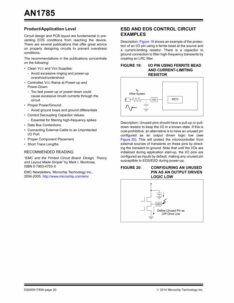
ESD AND EOS CONTROL CIRCUIT EXAMPLESDescription: Figure 19 shows an example of the protec-tion of an I/O pin using a ferrite bead at the source anda current-limiting resistor. There is a capacitor toground connection to filter high-frequency transients bycreating an LRC filter.
FIGURE 19: I/O PIN USING FERRITE BEAD AND CURRENT-LIMITING RESISTOR
Description: Unused pins should have a pull-up or pull-down resistor to keep the I/O in a known state. If this iscost-prohibitive, an alternative is to have an unused pinconfigured as an output driven logic low (seeFigure 20). This will protect the microcontroller fromexternal sources of transients on these pins by direct-ing the transient to ground. Note that until the I/Os areinitialized during application start-up, the I/O pins areconfigured as inputs by default, making any unused pinsusceptible to EOS/ESD during power-up.
FIGURE 20: CONFIGURING AN UNUSED PIN AS AN OUTPUT DRIVEN LOGIC LOW
MCUI/O
ToOther System
I/O
Define Unused Pin asO/P Drive Low
DS00001785A-page 20 2014 Microchip Technology Inc.
AN1785
Description: In PIC® microcontrollers, MCLR also servesas a VPP pin. This pin has no internal ESD clampingdiodes. It is necessary then, to protect the pin from ESDor EOS events. A current-limiting resistor, as shown (R2)in Figure 21, will limit the energy transferred to theMCLR pin during an ESD or EOS event.
FIGURE 21: USE OF CURRENT-LIMITING RESISTOR AND MCLR
Description: Figure 22 shows an example of decouplingthe power supply line. It is important to maintain a cleanpower feed to the microcontroller. Use a decouplingcapacitor close to the device’s VDD and VSS input pins tofilter out transients, and noise to the device. The bestpractice is to add a ferrite bead close to the power sourceto create an LC filter. Note that many devices may havemore than one VDD and VSS pin. Each pin pair shouldhave a decoupling capacitor as a standard practice.
FIGURE 22: DECOUPLING OF POWER SUPPLY LINE
Description: Figure 23 shows an example layout. Thereturn paths for the high-power, digital and analogblocks of the application circuit must be separated. Thiswill reduce the amount of switching noise, voltagespikes or transients transferred from one circuit block toanother. The grounds should be connected together atthe power supply entry point.
FIGURE 23: LAYOUT CONSIDERATIONS
R2 = 1 k
VDD
MCLR/VPP
PIC® MCUR1 = 10 k
0.1 F
Best
Better
VDD
VSS
VDD
VSS
High-PowerBlock
DigitalBlock
Ana
log
Blo
ck
High-Power Supply
High-Power Ground
Digital Supply
Digital Ground
Analog Supply
AIN
Analog Ground
2014 Microchip Technology Inc. DS00001785A-page 21
AN1785
Description: The transient suppressor devices havelimited current capability. Line impedance can beextremely low, so it is often necessary to include somelimiting resistance in series with the supply lines toreduce the stress on the shunt suppressors. Althoughresistors can be used, it is recommended that inductors
be used to increase efficiency and also add filtering(see Figure 24). This will help to reject line-borne noiseand will filter out power supply generated noise. Thewinding resistance and inductance can provide thenecessary series impedance to limit the transientcurrent for efficient transient suppression.
FIGURE 24: EFFICIENT TRANSIENT SUPPRESSION
Description: When using cables to connect to sensors,make sure to use the proper termination. Shieldedcabling is recommended (see Figure 25). In caseswhere a long cable is used, a 100 Ohm series resistor,
close to the microcontroller input, can help minimize theimpact of ESD events that may occur at the far end of thecable.
FIGURE 25: SHIELDED CABLING EXAMPLE
FUSE
V1120 Vac
C1MOV1 C2
L2
L1
Z3
Z2Z1C3 C4
L
N
GND
MOV3MOV2
Shielded Cable
DS00001785A-page 22 2014 Microchip Technology Inc.
AN1785
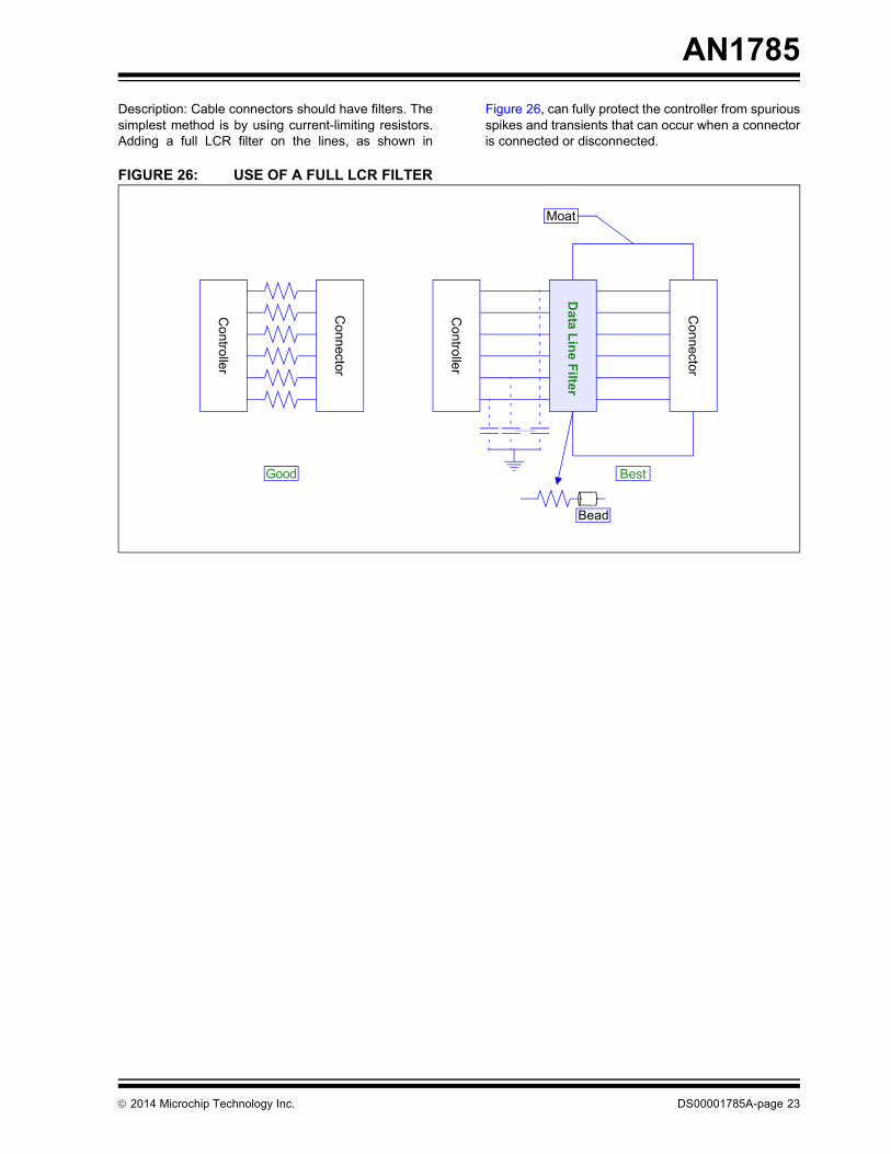
Description: Cable connectors should have filters. Thesimplest method is by using current-limiting resistors.Adding a full LCR filter on the lines, as shown in
Figure 26, can fully protect the controller from spuriousspikes and transients that can occur when a connectoris connected or disconnected.
FIGURE 26: USE OF A FULL LCR FILTER
Controller
Connector
Controller
Data Line Filter
Connector
Moat
Bead
BestGood
2014 Microchip Technology Inc. DS00001785A-page 23
AN1785
EXAMPLE FA REPORT
EOS Failure
BACKGROUNDA customer returned one USB82640AM unit for failureanalysis. USB Pins 3, 4 and 42 are shorted to ground.Power Pins 5, 15, 34, 26, 25, 16 and 12 are shorted toground.
SUMMARYFailure analysis was able to confirm a failure for thereturned unit. The device arrived with a crater in thepackage. There was no apparent damage to the leads.Several shorts were observed during curve tracer analy-sis, including I/Os (Pins 3, 4 and 42) as well as powerpins (Pins 5, 12, 15, 16, 25, 26 and 34). Anomalies wereobserved during X-ray analysis. The anomalies appearat the location of the package damage. Acousticmicroscopy revealed an anomaly at the location of thepackage damage. SN#1 was decapsulated using redfuming nitric acid. The unit was then thoroughlyinspected with a low-power microscope. EOS damagewas observed. The failure mechanism for SN#1 isdamage by Electrical Overstress.
ANALYSISEXTERNAL VISUAL: The device arrived with a craterin the package. There was no apparent damage to theleads (see Figure 27).
CURVE TRACE: Several shorts were observed duringcurve tracer analysis, including I/Os (Pins 3, 4 and 42)as well as power pins (Pins 5, 12, 15, 16, 25, 26 and34). The short observed on the mentioned pins isrepresented in Figure 28.
X-RAY/C-SAM ANALYSIS: Anomalies observed duringX-ray analysis. The anomalies appear at the location ofthe package damage (see Figure 29). Acousticmicroscopy revealed an anomaly at the location of thepackage damage (see Figure 30 and Figure 31).
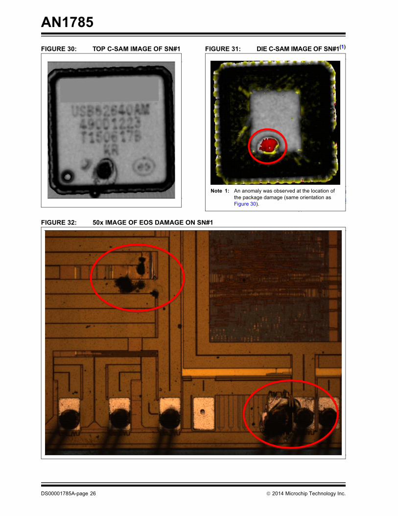
DECAPSULATION/ OPTICAL INSPECTION: SN#1was decapsulated using heated, fuming nitric acid. Theunit was then thoroughly inspected with a low-powermicroscope. EOS damage was observed (Figure 32).
CONCLUSION: The failure mechanism for SN#1 isdamage by Electrical Overstress.
DS00001785A-page 24 2014 Microchip Technology Inc.
AN1785
FIGURE 27: OPTICAL IMAGE OF SN#1
FIGURE 28: IMAGE OF SHORT OBSERVED ON SEVERAL I/O PINS AND POWER PINS
FIGURE 29: X-RAY IMAGE OF SN#1
2014 Microchip Technology Inc. DS00001785A-page 25
AN1785
FIGURE 30: TOP C-SAM IMAGE OF SN#1 FIGURE 31: DIE C-SAM IMAGE OF SN#1(1)
FIGURE 32: 50x IMAGE OF EOS DAMAGE ON SN#1
Note 1: An anomaly was observed at the location of the package damage (same orientation as Figure 30).
DS00001785A-page 26 2014 Microchip Technology Inc.
AN1785
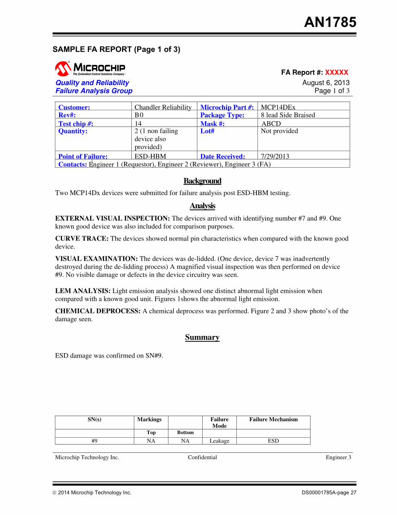
SAMPLE FA REPORT (Page 1 of 3)
�� �
FA Report #: �
Quality and Reliability� August 6, 2013�Failure Analysis Group Page 1 of 3
SN(s) Markings Failure
Mode Failure Mechanism
Top Bottom
#9 NA NA Leakage ESD Microchip Technology Inc. Confidential
Customer: Chandler Reliability Microchip Part #: MCP14DEx Rev#: B0 Package Type: 8 lead Side Braised Test chip #: 14 Mask #: Quantity: 2 (1 non failing
device also provided)
Lot# Not provided
Point of Failure: ESD-HBM Date Received: 7/29/2013 Contacts: (Requestor) (Reviewer), (FA)
Background
Two MCP14Dx devices were submitted for failure analysis post ESD-HBM testing.
Analysis
EXTERNAL VISUAL INSPECTION: The devices arrived with identifying number #7 and #9. One known good device was also included for comparison purposes.
CURVE TRACE: The devices showed normal pin characteristics when compared with the known good device.
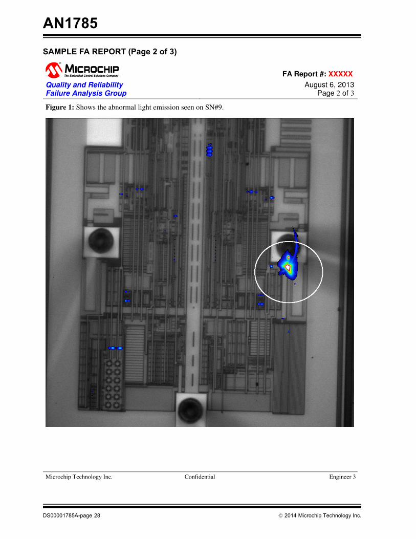
VISUAL EXAMINATION: The devices was de-lidded. (One device, device 7 was inadvertently destroyed during the de-lidding process) A magnified visual inspection was then performed on device #9. No visible damage or defects in the device circuitry was seen. LEM ANALYSIS: Light emission analysis showed one distinct abnormal light emission when compared with a known good unit. Figures 1shows the abnormal light emission.
CHEMICAL DEPROCESS: A chemical deprocess was performed. Figure 2 and 3 show photo’s of the damage seen.
Summary
ESD damage was confirmed on SN#9.
2014 Microchip Technology Inc. DS00001785A-page 27
AN1785
SAMPLE FA REPORT (Page 2 of 3)
�� �
FA Report #: �
Quality and Reliability� August 6, 2013�Failure Analysis Group Page 2 of 3
Microchip Technology Inc. Confidential
Figure 1: Shows the abnormal light emission seen on SN#9.
DS00001785A-page 28 2014 Microchip Technology Inc.
AN1785
SAMPLE FA REPORT (Page 3 of 3)
�� �
FA Report #: �
Quality and Reliability� August 6, 2013�Failure Analysis Group Page 3 of 3
Microchip Technology Inc. Confidential
Figure 2 and 3: Show the location and damage to SN#9. (Figure 2)
(Figure 3)
2014 Microchip Technology Inc. DS00001785A-page 29
AN1785
NOTES:
DS00001785A-page 30 2014 Microchip Technology Inc.
Note the following details of the code protection feature on Microchip devices:• Microchip products meet the specification contained in their particular Microchip Data Sheet.
• Microchip believes that its family of products is one of the most secure families of its kind on the market today, when used in the intended manner and under normal conditions.
• There are dishonest and possibly illegal methods used to breach the code protection feature. All of these methods, to our knowledge, require using the Microchip products in a manner outside the operating specifications contained in Microchip’s Data Sheets. Most likely, the person doing so is engaged in theft of intellectual property.
• Microchip is willing to work with the customer who is concerned about the integrity of their code.
• Neither Microchip nor any other semiconductor manufacturer can guarantee the security of their code. Code protection does not mean that we are guaranteeing the product as “unbreakable.”
Code protection is constantly evolving. We at Microchip are committed to continuously improving the code protection features of ourproducts. Attempts to break Microchip’s code protection feature may be a violation of the Digital Millennium Copyright Act. If such actsallow unauthorized access to your software or other copyrighted work, you may have a right to sue for relief under that Act.
Information contained in this publication regarding deviceapplications and the like is provided only for your convenienceand may be superseded by updates. It is your responsibility toensure that your application meets with your specifications.MICROCHIP MAKES NO REPRESENTATIONS ORWARRANTIES OF ANY KIND WHETHER EXPRESS ORIMPLIED, WRITTEN OR ORAL, STATUTORY OROTHERWISE, RELATED TO THE INFORMATION,INCLUDING BUT NOT LIMITED TO ITS CONDITION,QUALITY, PERFORMANCE, MERCHANTABILITY ORFITNESS FOR PURPOSE. Microchip disclaims all liabilityarising from this information and its use. Use of Microchipdevices in life support and/or safety applications is entirely atthe buyer’s risk, and the buyer agrees to defend, indemnify andhold harmless Microchip from any and all damages, claims,suits, or expenses resulting from such use. No licenses areconveyed, implicitly or otherwise, under any Microchipintellectual property rights.
2014 Microchip Technology Inc.
QUALITY MANAGEMENT SYSTEM CERTIFIED BY DNV
== ISO/TS 16949 ==
Trademarks
The Microchip name and logo, the Microchip logo, dsPIC, FlashFlex, flexPWR, JukeBlox, KEELOQ, KEELOQ logo, Kleer, LANCheck, MediaLB, MOST, MOST logo, MPLAB, OptoLyzer, PIC, PICSTART, PIC32 logo, RightTouch, SpyNIC, SST, SST Logo, SuperFlash and UNI/O are registered trademarks of Microchip Technology Incorporated in the U.S.A. and other countries.
The Embedded Control Solutions Company and mTouch are registered trademarks of Microchip Technology Incorporated in the U.S.A.
Analog-for-the-Digital Age, BodyCom, chipKIT, chipKIT logo, CodeGuard, dsPICDEM, dsPICDEM.net, ECAN, In-Circuit Serial Programming, ICSP, Inter-Chip Connectivity, KleerNet, KleerNet logo, MiWi, MPASM, MPF, MPLAB Certified logo, MPLIB, MPLINK, MultiTRAK, NetDetach, Omniscient Code Generation, PICDEM, PICDEM.net, PICkit, PICtail, RightTouch logo, REAL ICE, SQI, Serial Quad I/O, Total Endurance, TSHARC, USBCheck, VariSense, ViewSpan, WiperLock, Wireless DNA, and ZENA are trademarks of Microchip Technology Incorporated in the U.S.A. and other countries.
SQTP is a service mark of Microchip Technology Incorporated in the U.S.A.
Silicon Storage Technology is a registered trademark of Microchip Technology Inc. in other countries.
GestIC is a registered trademarks of Microchip Technology Germany II GmbH & Co. KG, a subsidiary of Microchip Technology Inc., in other countries.
All other trademarks mentioned herein are property of their respective companies.
Microchip received ISO/TS-16949:2009 certification for its worldwide
DS00001785A-page 31
headquarters, design and wafer fabrication facilities in Chandler and Tempe, Arizona; Gresham, Oregon and design centers in California and India. The Company’s quality system processes and procedures are for its PIC® MCUs and dsPIC® DSCs, KEELOQ® code hopping devices, Serial EEPROMs, microperipherals, nonvolatile memory and analog products. In addition, Microchip’s quality system for the design and manufacture of development systems is ISO 9001:2000 certified.
DS00001785A-page 32 2014 Microchip Technology Inc.
AMERICASCorporate Office2355 West Chandler Blvd.Chandler, AZ 85224-6199Tel: 480-792-7200 Fax: 480-792-7277Technical Support: http://www.microchip.com/supportWeb Address: www.microchip.comAtlantaDuluth, GA Tel: 678-957-9614 Fax: 678-957-1455Austin, TXTel: 512-257-3370 BostonWestborough, MA Tel: 774-760-0087 Fax: 774-760-0088ChicagoItasca, IL Tel: 630-285-0071 Fax: 630-285-0075ClevelandIndependence, OH Tel: 216-447-0464 Fax: 216-447-0643DallasAddison, TX Tel: 972-818-7423 Fax: 972-818-2924DetroitNovi, MI Tel: 248-848-4000Houston, TX Tel: 281-894-5983IndianapolisNoblesville, IN Tel: 317-773-8323Fax: 317-773-5453Los AngelesMission Viejo, CA Tel: 949-462-9523 Fax: 949-462-9608New York, NY Tel: 631-435-6000San Jose, CA Tel: 408-735-9110Canada - TorontoTel: 905-673-0699 Fax: 905-673-6509