2016 Microchip Technology Inc. DS00002049A-page 1 AN2049 INTRODUCTION This application note describes a drive solution for the Single-Phase Brushless DC (BLDC) motor. The feature-rich peripherals of Microchip’s PIC16F1618 enable the control of the H-bridge switches, set motor speed, predict rotor position, correct speed error, detect fault events, optimize commutation and ensure program memory data integrity. The solution described in this application note has the following key features: • Full-Bridge Motor Control • External PWM Speed Control • Software-Configurable, Hardware-Implemented PID • Overcurrent Detection • Overtemperature Detection • Motor Stall Detection • Supports IEC60730 Standard Class B Certification for Invariable Memory Testing BLOCK DIAGRAM Figure 1 shows the block diagram of a Single-Phase BLDC motor driver based on the PIC16F1618 microcontroller. The motor driver utilizes the Core Independent Peripheral (CIP) in the microcontroller to perform motor control function with minimum interven- tion from its Central Processing Unit (CPU). These are the CIPs used in the design: • Signal Measurement Timer (SMT) • Complementary Waveform Generator (CWG) • Cyclic Redundancy Checking (CRC/Scan) • Hardware Limit Timer (HLT) • Math Accelerator (MathACC) • Peripheral Pin Select (PPS) • Temperature Indicator (TempIndi) • Comparator (CMP) Combining the CIPs with other on-chip peripherals, such as I/O ports, Analog-to-Digital Converter (ADC), Fixed Voltage Reference (FVR), Digital-to-Analog Converter (DAC), Pulse-Width Modulation (PWM) and Timers, brings the intelligence of the whole system. These peripherals are internally connected by firmware, significantly reducing the number of external pins required for the implementation. Refer to Appendix A: “Circuit Schematic” for the detailed schematic diagram. FIGURE 1: BLOCK DIAGRAM Authors: Mike Gomez, Mark Pallones Microchip Technology Inc. Single-Phase BLDC Motor Driver
Transcript
AN2049Single-Phase BLDC Motor Driver
INTRODUCTION
This application note describes a drive solution for theSingle-Phase Brushless DC (BLDC) motor. Thefeature-rich peripherals of Microchip’s PIC16F1618enable the control of the H-bridge switches, set motorspeed, predict rotor position, correct speed error,detect fault events, optimize commutation and ensureprogram memory data integrity.
The solution described in this application note has thefollowing key features:
• Full-Bridge Motor Control• External PWM Speed Control• Software-Configurable, Hardware-Implemented
PID• Overcurrent Detection• Overtemperature Detection• Motor Stall Detection• Supports IEC60730 Standard Class B
Certification for Invariable Memory Testing
BLOCK DIAGRAM
Figure 1 shows the block diagram of a Single-PhaseBLDC motor driver based on the PIC16F1618microcontroller. The motor driver utilizes the CoreIndependent Peripheral (CIP) in the microcontroller toperform motor control function with minimum interven-tion from its Central Processing Unit (CPU). These arethe CIPs used in the design:
• Signal Measurement Timer (SMT)• Complementary Waveform Generator (CWG)• Cyclic Redundancy Checking (CRC/Scan)• Hardware Limit Timer (HLT)• Math Accelerator (MathACC)• Peripheral Pin Select (PPS)• Temperature Indicator (TempIndi)• Comparator (CMP)
Combining the CIPs with other on-chip peripherals,such as I/O ports, Analog-to-Digital Converter (ADC),Fixed Voltage Reference (FVR), Digital-to-AnalogConverter (DAC), Pulse-Width Modulation (PWM) andTimers, brings the intelligence of the whole system.
These peripherals are internally connected by firmware,significantly reducing the number of external pins requiredfor the implementation. Refer to Appendix A: “CircuitSchematic” for the detailed schematic diagram.
FIGURE 1: BLOCK DIAGRAM
Authors: Mike Gomez, Mark Pallones Microchip Technology Inc.
2016 Microchip Technology Inc. DS00002049A-page 1
AN2049
CONTROLLING THE MOTOR
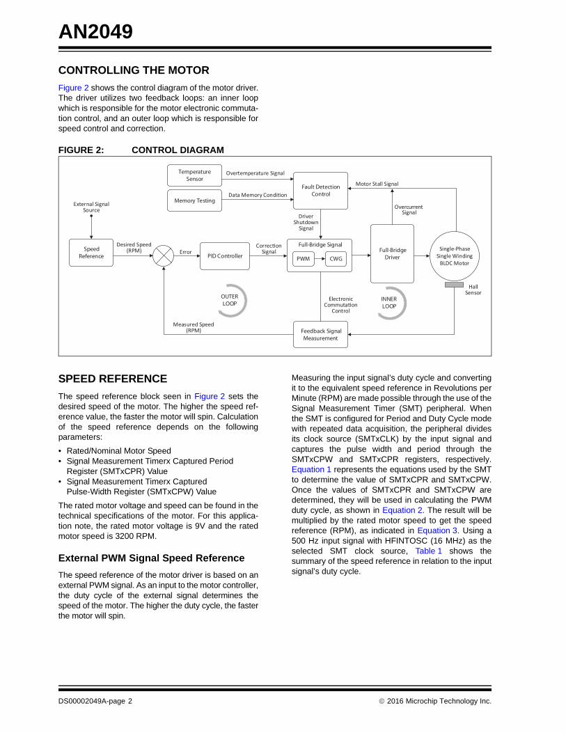
Figure 2 shows the control diagram of the motor driver.The driver utilizes two feedback loops: an inner loopwhich is responsible for the motor electronic commuta-tion control, and an outer loop which is responsible forspeed control and correction.
FIGURE 2: CONTROL DIAGRAM
SPEED REFERENCE
The speed reference block seen in Figure 2 sets thedesired speed of the motor. The higher the speed ref-erence value, the faster the motor will spin. Calculationof the speed reference depends on the followingparameters:
• Rated/Nominal Motor Speed • Signal Measurement Timerx Captured Period
Register (SMTxCPR) Value• Signal Measurement Timerx Captured
Pulse-Width Register (SMTxCPW) Value
The rated motor voltage and speed can be found in thetechnical specifications of the motor. For this applica-tion note, the rated motor voltage is 9V and the ratedmotor speed is 3200 RPM.
External PWM Signal Speed Reference
The speed reference of the motor driver is based on anexternal PWM signal. As an input to the motor controller,the duty cycle of the external signal determines thespeed of the motor. The higher the duty cycle, the fasterthe motor will spin.
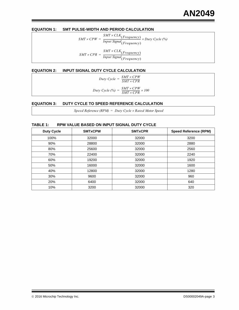
Measuring the input signal’s duty cycle and convertingit to the equivalent speed reference in Revolutions perMinute (RPM) are made possible through the use of theSignal Measurement Timer (SMT) peripheral. Whenthe SMT is configured for Period and Duty Cycle modewith repeated data acquisition, the peripheral dividesits clock source (SMTxCLK) by the input signal andcaptures the pulse width and period through theSMTxCPW and SMTxCPR registers, respectively.Equation 1 represents the equations used by the SMTto determine the value of SMTxCPR and SMTxCPW.Once the values of SMTxCPR and SMTxCPW aredetermined, they will be used in calculating the PWMduty cycle, as shown in Equation 2. The result will bemultiplied by the rated motor speed to get the speedreference (RPM), as indicated in Equation 3. Using a500 Hz input signal with HFINTOSC (16 MHz) as theselected SMT clock source, Table 1 shows thesummary of the speed reference in relation to the inputsignal’s duty cycle.
Full-Bridge SignalSpeed
Reference PID Controller
Feedback Signal Measurement
Full-Bridge Driver
Single-Phase Single Winding
BLDC Motor
Hall Sensor
Measured Speed (RPM)
Electronic Commuta on
Control
ErrorDesired Speed
(RPM)Correc on
Signal
Fault Detection Control
Temperature Sensor
Driver Shutdown
Signal
Overtemperature Signal
Motor Stall Signal
Overcurrent Signal
OUTER LOOP
PWM CWG
Memory Testing Data Memory Condi on
External Signal Source
INNER LOOP
DS00002049A-page 2 2016 Microchip Technology Inc.
AN2049
EQUATION 1: SMT PULSE-WIDTH AND PERIOD CALCULATION
EQUATION 2: INPUT SIGNAL DUTY CYCLE CALCULATION
EQUATION 3: DUTY CYCLE TO SPEED REFERENCE CALCULATION
SMT CPWSMT CLK Frequency
Input Signal Frequency ---------------------------------------------------------------- Duty Cycle (%)=
SMT CPRSMT CLK Frequency
Input Signal Frequency ----------------------------------------------------------------=
Speed Reference (RPM) Duty Cycle Rated Motor Speed=
TABLE 1: RPM VALUE BASED ON INPUT SIGNAL DUTY CYCLE
Duty Cycle SMTxCPW SMTxCPR Speed Reference (RPM)
100% 32000 32000 3200
90% 28800 32000 2880
80% 25600 32000 2560
70% 22400 32000 2240
60% 19200 32000 1920
50% 16000 32000 1600
40% 12800 32000 1280
30% 9600 32000 960
20% 6400 32000 640
10% 3200 32000 320
2016 Microchip Technology Inc. DS00002049A-page 3
AN2049
INNER LOOP
In a Single-Phase BLDC motor, the four-slot statorcontains the windings and the rotor is a four-pole per-manent magnet. Figure 3 shows the standard structureof a Single-Phase BLDC motor. The rotor is the onethat produces the rotating motion of the motor. To makethe rotor spin, there must be a rotating magnetic field
produced by the stator. The single winding iselectrically activated to create a rotating field. To pro-vide continuous rotation and prevent the permanentmagnet rotor from getting locked with the stator, theexcitation on the stator winding must be sequenced ina specific manner while knowing the exact position ofthe rotor magnets. The rotor magnet position isdetermined by using a Hall effect sensor.
FIGURE 3: SINGLE-PHASE BLDC MOTOR STRUCTURE
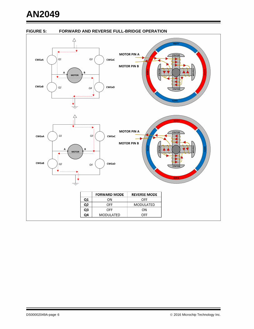
Figure 4 shows the timing control based on the Hallsensor. The Complementary Waveform Generator(CWG) output, which controls the excitation of the statorwinding, is dependent on the state of the Hall sensor out-put. In order to control the CWG output, the Hall sensoroutput is compared to a Fixed Voltage Reference (FVR)by the comparator. The comparator hysteresis is enabledto disregard the noise that might add to the Hall sensoroutput. The output of the comparator toggles theCWG1MODE0 bit of CWG’s CWG1CON0 register. Whenthe CWG1MODE0 bit is active, the CWG output is inForward Full-Bridge mode and when inactive, the CWGoutput is in Reverse Full-Bridge mode. The toggling fromForward-to-Reverse mode produces a clockwise rotation,while toggling from Reverse-to-Forward mode producesa counter-clockwise rotation.
The CWG output is fed to the switches’ input of thefull(H)-bridge circuit. Figure 5 shows the forward andreverse full-bridge operation and the correspondingmagnetic polarity that the four-slot stator shouldproduce based on the CWG output. In Forward mode,Q1 is on, Q2 and Q3 are off and Q4 is modulated. Whilein Reverse mode, Q1 and Q4 are off, Q2 is modulatedand Q3 is on. In order to produce one electrical cycle,a forward-reverse combination must be executed. Onemechanical revolution of the motor requires twoelectrical cycles, therefore, two forward-reversecombinations must be executed to complete a singleclockwise rotation of the motor.
STATOR
STATOR COILSSTATOR COILSHALL SENSOR FAN BLADE
ROTOR
STATOR
STATOR
STATOR
STAT
OR
MOTOR PIN A
MOTOR PIN B
DS00002049A-page 4 2016 Microchip Technology Inc.
AN2049
FIGURE 4: SENSOR AND DRIVE TIMING DIAGRAM
Comp/Hall Sensor
CWG1A
CWG1B
CWG1C
CWG1D
CWG Input Source
(PWM3)
0 90 180 270 0 90 180
Forward Mode Reverse Mode Forward ModeCWG1MODE
270 0
Reverse Mode
+V
-V+V
-V
+V
GND
+V
GND
+V
GND
+V
GND
+V
GND
+V
GND
Motor Pin A
Motor Pin B
1 Electrical Cycle 1 Electrical Cycle
1 Mechanical Cycle (1 Rotation)
2016 Microchip Technology Inc. DS00002049A-page 5
AN2049
FIGURE 5: FORWARD AND REVERSE FULL-BRIDGE OPERATION
MOTOR PIN A
MOTOR PIN B
STATOR
STAT
OR STATO
R
STATOR
NORTH
NORTH
SOU
TH SOU
TH
MOTOR PIN A
MOTOR PIN B
STATOR
STAT
OR STATO
R
STATOR
CWGxA
MOTOR
CWGxC
CWGxB CWGxD
Q1 Q3
Q2 Q4
A B
CWGxA
MOTOR
CWGxC
CWGxB CWGxD
Q1 Q3
Q2 Q4
A B
DS00002049A-page 6 2016 Microchip Technology Inc.
AN2049
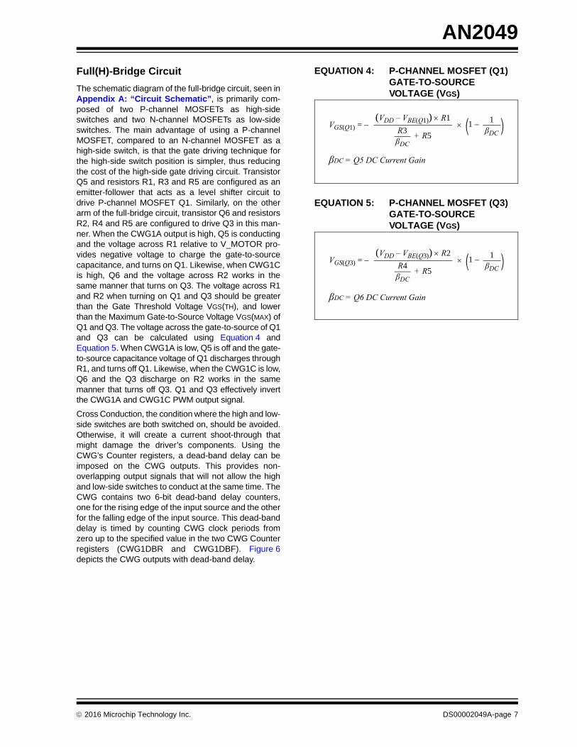
Full(H)-Bridge Circuit
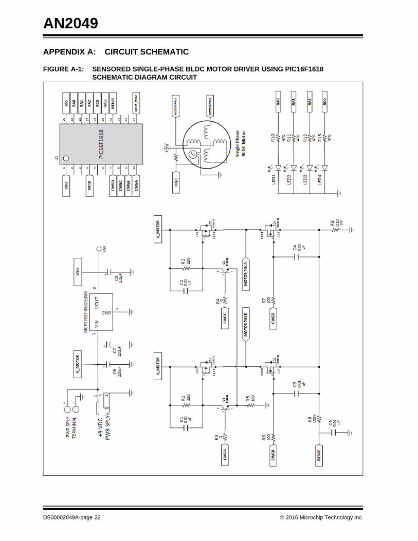
The schematic diagram of the full-bridge circuit, seen inAppendix A: “Circuit Schematic”, is primarily com-posed of two P-channel MOSFETs as high-sideswitches and two N-channel MOSFETs as low-sideswitches. The main advantage of using a P-channelMOSFET, compared to an N-channel MOSFET as ahigh-side switch, is that the gate driving technique forthe high-side switch position is simpler, thus reducingthe cost of the high-side gate driving circuit. TransistorQ5 and resistors R1, R3 and R5 are configured as anemitter-follower that acts as a level shifter circuit todrive P-channel MOSFET Q1. Similarly, on the otherarm of the full-bridge circuit, transistor Q6 and resistorsR2, R4 and R5 are configured to drive Q3 in this man-ner. When the CWG1A output is high, Q5 is conductingand the voltage across R1 relative to V_MOTOR pro-vides negative voltage to charge the gate-to-sourcecapacitance, and turns on Q1. Likewise, when CWG1Cis high, Q6 and the voltage across R2 works in thesame manner that turns on Q3. The voltage across R1and R2 when turning on Q1 and Q3 should be greaterthan the Gate Threshold Voltage VGS(TH), and lowerthan the Maximum Gate-to-Source Voltage VGS(MAX) ofQ1 and Q3. The voltage across the gate-to-source of Q1and Q3 can be calculated using Equation 4 andEquation 5. When CWG1A is low, Q5 is off and the gate-to-source capacitance voltage of Q1 discharges throughR1, and turns off Q1. Likewise, when the CWG1C is low,Q6 and the Q3 discharge on R2 works in the samemanner that turns off Q3. Q1 and Q3 effectively invertthe CWG1A and CWG1C PWM output signal.
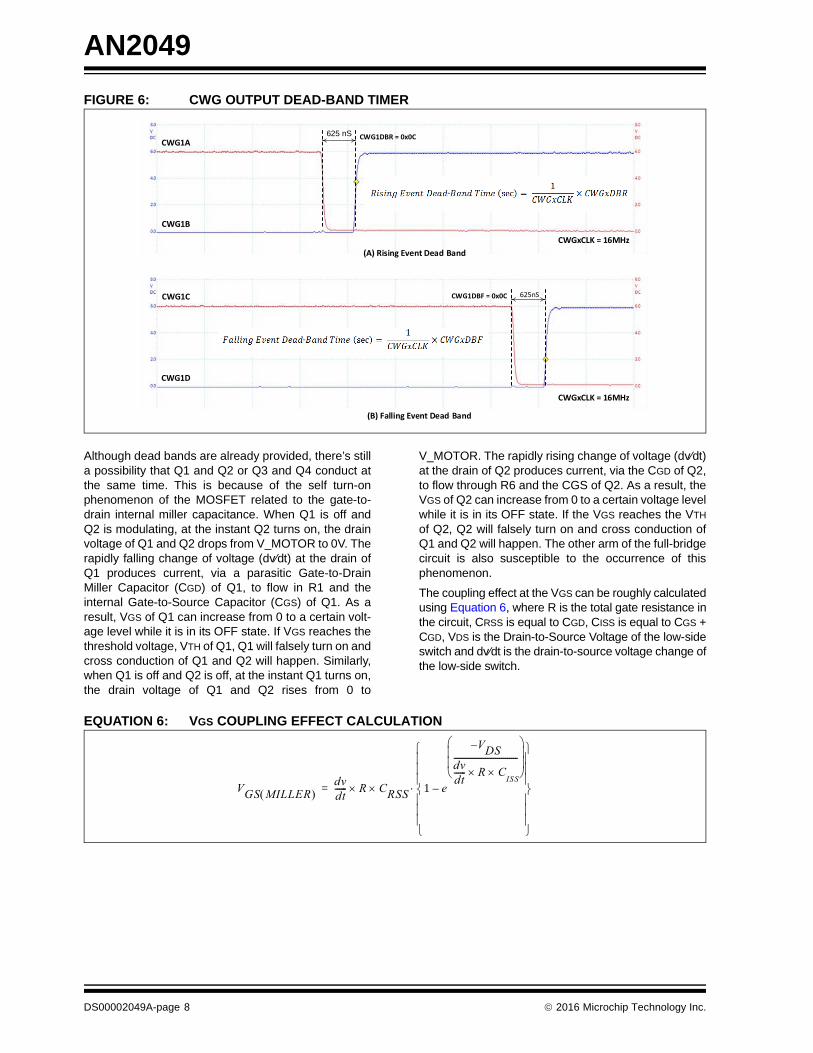
Cross Conduction, the condition where the high and low-side switches are both switched on, should be avoided.Otherwise, it will create a current shoot-through thatmight damage the driver’s components. Using theCWG’s Counter registers, a dead-band delay can beimposed on the CWG outputs. This provides non-overlapping output signals that will not allow the highand low-side switches to conduct at the same time. TheCWG contains two 6-bit dead-band delay counters,one for the rising edge of the input source and the otherfor the falling edge of the input source. This dead-banddelay is timed by counting CWG clock periods fromzero up to the specified value in the two CWG Counterregisters (CWG1DBR and CWG1DBF). Figure 6depicts the CWG outputs with dead-band delay.
EQUATION 4: P-CHANNEL MOSFET (Q1) GATE-TO-SOURCE VOLTAGE (VGS)
EQUATION 5: P-CHANNEL MOSFET (Q3) GATE-TO-SOURCE VOLTAGE (VGS)
βDC = Q5 DC Current Gain
VGS(Q1) = –(VDD – VBE(Q1)) R1
R3βDC
+ R5( )1 – 1
βDC
βDC = Q6 DC Current Gain
VGS(Q3) = –(VDD – VBE(Q3)) R2
R4βDC
+ R5( )1 – 1
βDC
2016 Microchip Technology Inc. DS00002049A-page 7
AN2049
FIGURE 6: CWG OUTPUT DEAD-BAND TIMER
Although dead bands are already provided, there’s stilla possibility that Q1 and Q2 or Q3 and Q4 conduct atthe same time. This is because of the self turn-onphenomenon of the MOSFET related to the gate-to-drain internal miller capacitance. When Q1 is off andQ2 is modulating, at the instant Q2 turns on, the drainvoltage of Q1 and Q2 drops from V_MOTOR to 0V. Therapidly falling change of voltage (dv⁄dt) at the drain ofQ1 produces current, via a parasitic Gate-to-DrainMiller Capacitor (CGD) of Q1, to flow in R1 and theinternal Gate-to-Source Capacitor (CGS) of Q1. As aresult, VGS of Q1 can increase from 0 to a certain volt-age level while it is in its OFF state. If VGS reaches thethreshold voltage, VTH of Q1, Q1 will falsely turn on andcross conduction of Q1 and Q2 will happen. Similarly,when Q1 is off and Q2 is off, at the instant Q1 turns on,the drain voltage of Q1 and Q2 rises from 0 to
V_MOTOR. The rapidly rising change of voltage (dv⁄dt)at the drain of Q2 produces current, via the CGD of Q2,to flow through R6 and the CGS of Q2. As a result, theVGS of Q2 can increase from 0 to a certain voltage levelwhile it is in its OFF state. If the VGS reaches the VTH
of Q2, Q2 will falsely turn on and cross conduction ofQ1 and Q2 will happen. The other arm of the full-bridgecircuit is also susceptible to the occurrence of thisphenomenon.
The coupling effect at the VGS can be roughly calculatedusing Equation 6, where R is the total gate resistance inthe circuit, CRSS is equal to CGD, CISS is equal to CGS +CGD, VDS is the Drain-to-Source Voltage of the low-sideswitch and dv⁄dt is the drain-to-source voltage change ofthe low-side switch.
EQUATION 6: VGS COUPLING EFFECT CALCULATION
625nS CWG1DBR = 0x0C
625nSCWG1DBF = 0x0C
(A) Rising Event Dead-Band
(B) Falling Event Dead-Band
CWG1A
CWG1B
CWG1C
CWG1D
CWGxCLK = 16MHz
CWGxCLK = 16MHz
625 nS
-
-
VGS MILLER dvdt------ R CRSS 1 e
V– DSdvdt------ R C
ISS
--------------------------------
–
=
DS00002049A-page 8 2016 Microchip Technology Inc.
AN2049
In order to reduce the internal coupling effect, an externalcapacitor is connected across the gate-to-source termi-nal of the MOSFETs. In the schematic diagram, C1, C2,C3 and C4 are connected across the gate-to-sourceterminals of Q1, Q2, Q3 and Q4, respectively. Thesecapacitors increase the effective CISS for each respectiveMOSFET. For example, when C1 is connected acrossthe gate-to-source of Q1, the effective value of the CISS
of Q1 is equal to CGS + CGD + C1. In reference toEquation 6, when CISS increases, the VGS of Q1, due toMiller coupling, decreases.
In this application, the key parameters in selectingMOSFETs are based on the device RDS(ON) (On-Resistance) and QG (Total Gate Charges). Ideally, theN-channel and P-channel MOSFETs in the full-bridgecircuit should have the same RDS(ON) and QG in order toattain the optimal switching performance. Therefore,it is convenient to choose a complementary pair of aP-channel and an N-channel device in order to matchthese parameters. However, this is impossible due to thedifference of construction of the two MOSFETs. The chipsize of the P-channel must be two to three times that ofthe N-channel in order to match the N-channel RDS(ON)performance, but the larger the chip size, the larger theeffect on its dynamic performance, such as QG. On theother side, when the P-channel has the same QG as theN-channel, the P-channel and N-channel have the samechip size, but the P-channel has larger RDS(ON) than theN-channel. Because of this trade-off, it will be necessaryto choose which parameter between RDS(ON) and QG willmostly affect the switching performance of the MOSFET.The decision is determined based on the MOSFET’soperating switching frequency. At high-frequencyoperation (greater than 50 kHz), switching losses aredominant. When the QG of P-channel is comparable withthe N-channel MOSFET, it will significantly reduce thetotal MOSFET power losses. Otherwise, at low-frequencyoperation (less than 50 kHz), conduction losses are dom-inant. When RDS(ON) of the P-channel is comparable withthe N-channel MOSFET, it will significantly reduce thetotal MOSFET power losses. In this motor driver solution,the switching frequency is 15.625 kHz; therefore, theP-channel and N-channel MOSFETs were chosenthrough their comparable RDS(ON), as shown in Table 2.
TABLE 2: MOSFET CHARACTERISTICS (QG AND RDS(ON))
MOSFET Type
P/N QG RDS(ON)
P-Channel FDS6375 26 nC 0.024at VGS = -4.5V
N-Channel NDS8425 11 nC 0.022at VGS = 4.5V
Note: An alternate Micrel MOSFET driver canalso be used with the designed full-bridgecircuit in this application note. Refer towww.micrel.com for the complete list ofavailable full-bridge drivers.
The outer loop, shown in Figure 2, provides measure-ment and control of the motor’s speed. The objective incontrolling the motor’s speed is to maintain the speed ofthe motor at the desired value under various conditions,such as change in load demand, disturbances and tem-perature drift. To implement an outer loop control, themotor’s actual speed should be determined by applyingnecessary speed correction to maintain the desired value.
Actual Speed Measurement
Aside from calculating the desired speed reference,SMT is also used to measure the actual motor speedresponse. Measuring the motor’s actual speed is donethrough the use of SMT Period and Duty Cycle Acqui-sition mode with repeated data acquisition. By enablingthis mode, the peripheral will automatically measurethe period of the input signal (SMTxIN) relative to theSMTx clock source (SMTxCLK) and the result will bestored in the SMTx Captured Period register(SMTxCPR), as shown in Equation 7. By combiningEquation 7 and the general formula of the BLDC motorfor calculating RPM, shown in Equation 8, the actualspeed of the motor in RPM can be calculated asdemonstrated in Equation 9.
EQUATION 7: SMT CAPTURED PERIOD REGISTER CALCULATION
EQUATION 8: MOTOR RPM CALCULATION
EQUATION 9: COMBINED EQUATION TO CALCULATE ACTUAL SPEED
The speed reference described in Equation 3 and actualspeed described in Equation 9 are now compared todetermine the error. This error can be positive ornegative, which indicates that the actual speed is higheror lower than the speed reference. This error is fed to aPID controller to calculate a value that compensates thevariation in speed.
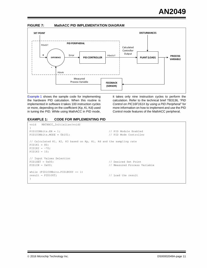
The PID controller is an algorithm that provides stabilityin a system. It is usually implemented through software,which takes several instructions in performing a series ofoperation and iteration. In contrast with the usual imple-mentation of the PID, the PID controller used in thisdesign uses the on-chip MathACC with PID modemodule of the PIC16F1618. This hardware-implementedPID performs the calculation very efficiently in thediscrete time domain.
Figure 7 shows that the calculated speed reference isused as the PIDx Set Point (PIDxSET) while the actualspeed of the motor is used as the PIDx Input(PIDxIN).The module will automatically calculate thecompensating value and yield it as a PIDx Output(PIDxOUT). This value will be used to adjust the dutycycle of the CWG PWM output.
Number of Poles-----------------------------------------------------------=
Actual Speed (RPM)120 SMT CLK
Number of Poles SMT CPR-------------------------------------------------------------------------------=
DS00002049A-page 10 2016 Microchip Technology Inc.
AN2049
FIGURE 7: MathACC PID IMPLEMENTATION DIAGRAM
Example 1 shows the sample code for implementingthe hardware PID calculation. When this routine isimplemented in software it takes 100 instruction cyclesor more, depending on the coefficient (Kp, Ki, Kd) usedin tuning the PID. While using MathACC in PID mode,
it takes only nine instruction cycles to perform thecalculation. Refer to the technical brief TB3136, “PIDControl on PIC16F161X by using a PID Peripheral” formore information on how to implement and use the PIDControl mode features of the MathACC peripheral.
// Calculated K1, K2, K3 based on Kp, Ki, Kd and the sampling rate PID1K1 = 80;PID1K2 = -70;PID1K3 = 10;
// Input Values Selection PID1SET = 0x00; // Desired Set PointPID1IN = 0x00; // Measured Process Variable
while (PID1CONbits.PID1BUSY == 1) result = PID1OUT; // Load the result}
2016 Microchip Technology Inc. DS00002049A-page 11
AN2049
MOTOR DRIVER PROTECTION FEATURE
In order to avoid system failure, damage or motor driverperformance degradation, appropriate early Faultdetection strategies are implemented in this application.
Overcurrent Detection
Exceeding the motor’s maximum allowable torqueloading can cause the motor winding to take themaximum allowed current, which may cause the motorto rise above its allowed operating temperature. Toprotect the motor from overheating, Fault detection forovercurrent must be implemented.
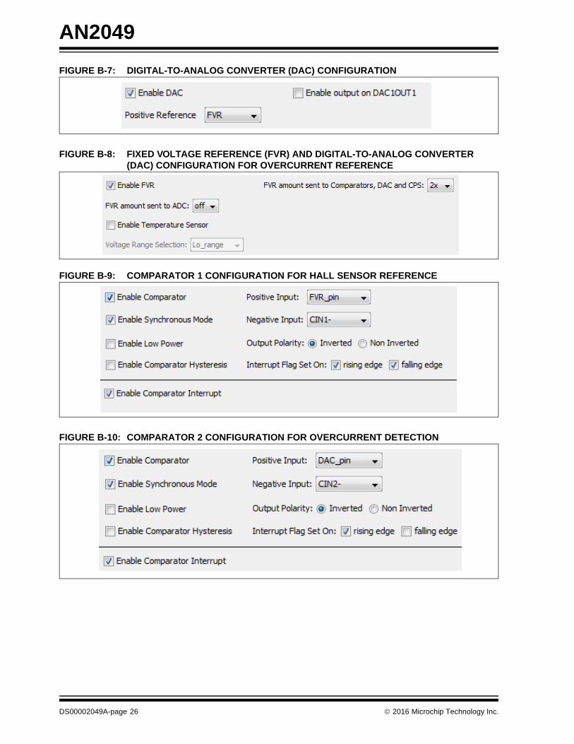
To implement overcurrent detection, an RSHUNT isadded to the drive circuitry that gives a voltage corre-sponding to the current flowing in the motor winding. Thevoltage drop across this resistor varies linearly withrespect to the motor current. The voltage is fed to theinverting input of the comparator and compared to acertain reference voltage. This reference voltage isbased on the result between the RSHUNT resistance andthe maximum allowable stall current of the motor. Thereference voltage can be provided by the FVR, whichcan be narrowed down further by the DAC. In thismanner, a very small reference voltage can be used,
allowing the RSHUNT resistance to be kept low. Keepingthe resistance low reduces the RSHUNT power dissipa-tion. If the RSHUNT voltage exceeds the reference, thecomparator output will trigger the auto-shutdown featureof the CWG.
Overtemperature Detection
Overtemperature can be detected using the deviceon-chip temperature indicator peripheral present withinthe PIC16F161X family. The indicator measures thedevice temperature, corresponding to the temperaturein its environment with some delay.
The indicator is used to measure the device temperaturebetween -40°C and +85°C. The internal circuit of thetemperature indicator produces a variable voltage rela-tive to temperature using an internal transistor junctionthreshold voltage. This voltage is converted to a digitalform by the Analog-to-Digital Converter (ADC). TheADC result will be used to determine the actual tempera-ture reading defined by Equation 10. For a moreaccurate temperature indicator reading, a single-pointcalibration is implemented. Refer to the application noteAN1333, “Use and Calibration of the Internal Tempera-ture Indicator” for more details regarding the calibrationprocess.
Note: High-Range mode = 4 Low-Range mode = 2 n = Number of bits of ADC Resolution ADCRESULT = ADRES Register Value
DS00002049A-page 12 2016 Microchip Technology Inc.
AN2049
The implementation of the overtemperature detectionuses the ADC internal Channel Input Selection (CHS)bit. The Temperature Indicator (TempInd) module isused as the channel input for the ADC. For every timerinterrupt, the completed ADC conversion result will becompared to the desired maximum temperature limit.When the ADC result exceeds the maximum temperaturelimit, the output of the CWG disables.
Table 3 summarizes the ADC result that the temperatureindicator produces relative to the temperature.
Motor Stall Detection
When the motor is spinning, the Hall sensor providesperiodic pulses. If the motor stalls, the Hall sensor alsostops from providing the pulses. The controller uses theHall sensor response to detect the motor stalledcondition. To implement the motor stall detection, theedge-triggered Hardware Limit Timer (HLT) mode inthe Timer2/4/6 peripheral is used. Its main function is tomonitor any changes in a periodic signal and iseffectively set up as a retriggerable monostable. Referto Figure 8 for HLT implementation on motor controldesign.
FIGURE 8: HLT STALL DETECTION
TABLE 3: TEMPERATURE INDICATOR ADC RESULT SUMMARY
Temperature (°C)
VTEMP mV8-Bit ADC
Result10-Bit ADC
Result
-40 2,364 121 484
-30 2,4168 123 494
-20 2,4696 126 505
-10 2,5224 129 516
0 2,5752 131 527
10 2,628 134 538
20 2,6808 137 548
30 2,7336 139 559
40 2,7864 142 570
50 2,8392 145 581
60 2,892 147 592
70 2,9448 150 603
80 2,9976 153 613
85 3,024 154 619
Hall Sensor
C1
Full-Bridge Driver
Single-Phase BLDC Motor
CWG
FVR
/4/2 Shutdown Signal
Timer2 HLT Mode
2016 Microchip Technology Inc. DS00002049A-page 13
AN2049
In this application, the Comparator 1 output, which isconnected to the Hall sensor signal, is set as the exter-nal signal source for the HLT. The Hall sensor producessignals ranging from 32 Hz (31.25 mS) up to 110 Hz(9 mS) depending on the motor speed. The Period(PR2) register of the Timer2 is then set to a value thatis sufficiently larger than the minimum input frequency(32 Hz). By doing this, motor stall condition can bedetected at a much wider speed range. Refer toEquation 11 for the PR2 value calculation based on theHall sensor’s signal.
EQUATION 11: PR2 CALCULATION
The reason for a larger PR2 value is for the Hall sensorpulse to occur first and reset the Timer2 count beforethe PR2 period match occurs. In case of a rotatingmotor, Hall sensor pulses are always present to contin-uously reset the Timer2 count, avoiding the periodmatch to occur. Otherwise, in case of a stalled motor,Hall sensor pulses are not present to reset the Timer2count, hence the timer continues to increment until theperiod match occurs. An interrupt event is triggeredevery time a period match occurs. This can be used toshut down the CWG output and indicate that the motoris not spinning or is in a stalled condition. Refer toFigure 9 for the implementation of HLT mode as stalldetection.
FIGURE 9: STALL DETECTION IMPLEMENTATION
PR2TMR2 Clock Source
Input Signal MIN Prescaler Postscaler-------------------------------------------------------------------------------------------------------------------
PR2LFINTOSC
35 Hz------------------------------
3100032 1 8------------------------ 121
Note: PR2 register value should be greater than 121.
Hall Sensor
Motor Normal Running Condition
Motor Stall Condition
150PR2 Value
Timer Clock
Timer Count
Reset Signal1 2 3 4 5 . . .
121
1 2 3 4 5 . . .
Timer Interrupt
Motor stalled at this point
150
Timer Clock
Timer Count 1 2 3 4 5 . . .
121
Timer Interrupt
PR2 Value
150 PR2 and Timer Count Matched at this point
(PR2 Match)
Hall Sensor
Start Timer Count at Rising Edge
Start Timer Count at Rising Edge
DS00002049A-page 14 2016 Microchip Technology Inc.
AN2049
Program Memory Data Monitoring and Checking
In a motor control application, data integrity is necessaryto ensure the safe operation of the motor and all theFault detection features are functioning reliably. A failurein the implementation of the motor function and all itssafety features, due to corrupted program memory, mayresult in the damage of the drivers and of the controlcircuitry. To avoid this scenario, an error detectiontechnique can be added in the control system to monitorthe program memory data integrity. Using the CyclicRedundancy Check (CRC) peripheral, along with thebuilt-in Program Memory Scan module, a memory testprocedure can be performed periodically during systemrun time without conflicting with the motor’s operation.This hardware CRC periodic memory test implementa-tion is also helpful in complying with the IEC 60730standard Class B certification in invariable memory(Flash/EEPROM) test. Refer to the application noteAN1799, “Class B Safety Software Library for 8-bit PIC®
MCUs”, for more details regarding the program memorychecking compliance procedure according to theIEC-60730 standard Class B certification.
The CRC peripheral provides a means for calculating acheck value (checksum) of the program memory. Byusing the built-in Program Memory Scanner module,program memory can be converted into equivalentbinary data and used as input data (CRCDAT) to theCRC. The CRC checksum (CRCACC) is generated bydividing the CRC input data (CRCDAT) by anotherbinary number, called the CRC polynomial (CRCXOR).The CRC polynomial can be any polynomial up to17 bits, or any commonly used standard polynomials,such as CRC-16-ANSI/0x8005, CRC-8/0xD5 andCRC-16/CCITT/0x1021. Figure 10 shows the simplifiedblock diagram of CRC implementation in this applica-tion. Refer to the technical brief TB3128, “CRC andMemory Scan on 8-Bit Microcontrollers Technical Brief”for more details regarding the implementation of CRCand memory scan.
FIGURE 10: CRC AND MEMORY SCAN SIMPLIFIED BLOCK DIAGRAM
MEMORY SCAN
Scan Program Memory Addresses Indicate the desired program memory addresses to be scanned
Generate Equivalent Binary Data
CRC DATA
PROGRAM MEMORY SCAN MODULE
CRC DATA(CRCDATH/L)
CRC POLYNOMIAL
Pre-Define Polynomials
CRC-16/0x8005 CRC-8/0xD5 CRC-16-CCITT/0x1021
Result Checksum(CRCACCH/L)
CRC MODULEProgram Memory Scan
CRC DATA SOURCEUser Define
CRC DATA SOURCE
CRC CALCULATION
2016 Microchip Technology Inc. DS00002049A-page 15
AN2049
At the first system start-up, an initial memory scan isperformed at the whole program memory addressusing the Burst mode operation. The Burst mode pro-duces the highest scanner throughput at the expenseof stalling other CPU functions. Therefore, it is usuallyused only during start-up. Scanner output will be usedby the CRC to calculate the reference checksum value.Then, during the system run time, the scanner and theCRC calculation are periodically called to generateanother checksum value of the same program memory
address. The scanner scans in Peek mode to avoid thestalling of other CPU functions, but it produces thelowest scanner throughput. If the reference and theperiodically generated checksum values match, anindicator can be set by the user to indicate that the pro-gram memory has passed the test and no errors werefound. In case of a failed program memory testing, or incase errors were found, the CWG output shutdown willbe triggered. Figure 11 shows the diagram of the CRCcalculation routine used in this application.
FIGURE 11: CRC AND MEMORY SCAN IMPLEMENTATION ROUTINE
AT SYSTEM START- -UP
START
Ini lize St rt-up Progr m Memory Sc n
CRCFLAG = 0?
Ini lize CRC C lcul on
Store C lcul tedReference Checksum V lue
Set CRCFLAG = 1;
END
Ini lize other Peripher ls
Execute Motor Func on
DURING SYSTEM RUN TIME
Comp re Reference Checksum nd Periodic Checksum V lue
Ini lize Periodic Progr m Memory Sc n
Ini lize CRC C lcul on
Sign l n Error Stop l Control
Check for Mism tch
Peek Mode Sc nning
Periodic Checksum C lcul on
YES NO
DS00002049A-page 16 2016 Microchip Technology Inc.
AN2049
MOTOR DRIVER FIRMWARE
FIGURE 12: FIRMWARE FLOWCHART
Figure 12 shows the motor driver firmware flowchart.During system start-up, the firmware initializes theperipherals and the connection amongst each other.After peripherals are initialized, the firmware enablesthe program memory scan and runs a CRC calculationto determine the initial checksum value of the programmemory. This value is used as a reference andperiodically compared with another checksum value,generated during system run time, to check and ensurethe integrity of the program memory data.
PID_Routine
Reset Sampling Time (Timer1)
Set PID Inputs (PIDxIN, PIDxSET)
PID Calculation Done?
Load New PWM Value
Clear PID Flag
YES
NO
START
Initialization(I/O, ADC, Timer, PWM3, CWG,
Comparator, DAC, FVR, SMT, MATHACC, CRC)
SpeedReference_Calculation()
PID Flag Set?
Do PID_Routine()
NO
Burst Mode Memory Scan
Reference Checksum Calculation
Input Signal Available?
ActualSpeed_Calculation()
SMT1 Result to RPM Conversion
SMT2 Result to RPM Conversion
YES
CRCFlag = 0?YES
NO
CRCFlag = 1;
NO
YES
2016 Microchip Technology Inc. DS00002049A-page 17
AN2049
After all the initialization, the firmware will enter acontinuous loop, allowing the execution of the followingrepeated tasks:
1. Monitors the changes in the duty cycle of theinput PWM signal and updates the speed refer-ence setting. This task is performed by theSpeedReference_Calculation() routine.
2. Monitors the changes in the actual motor speedresponse and updates the speed reading. Thistask is performed by the ActualSpeed_Calculation() routine.
3. Monitors every Timer1 overflow interrupt andsignals the firmware to start the PID calculation.Timer1 overflow corresponds to the desired PIDcontroller sampling time and is equivalent to10ms for this application.
FIGURE 13: TIMER3, COMPARATOR 1 AND COMPARATOR 2 FLOWCHART
Over Current Detected
Comparator2 ISR
Shutdown CWG Module
Over Temperature?
ADC Ready?
Calibrate Temperature Indicator Module
Get Temperature Reading
Clear Timer Flag
Set ADC Channel to Temperature Indicator
Shutdown CWG Module
Timer3 ISR(Every 300secs)
YES
NO
RETURN
Turn ON Over TemperatureLED Indicator
Turn ON Over Current LED Indicator
(ADRESH:L) ± (Calibration Value)
Comparator1 ISR
Is MC1OUT High?
YES
NO
CWG Reverse Mode
RETURN
CWG Forward Mode
DS00002049A-page 18 2016 Microchip Technology Inc.
AN2049
FIGURE 14: HLT AND TIMER4 ISR FLOWCHART
Additionally, the firmware executes several InterruptService Routines (ISRs) indicating a certain motorcondition. These interrupt handlers are automaticallyexecuted when certain peripheral criteria have beenmet. Refer to Figure 13 and Figure 14 for the peripheralISR flowchart.
1. Comparator 1 ISR – Monitors the motor’s Hallsensor signal. This is executed every change ofHall sensor output state. When the Hall sensorsignal is high, the CWG Forward mode isenabled, otherwise, the CWG Reverse mode isenabled.
2. Comparator 2 ISR – Monitors the systemovercurrent. This is executed on every risingedge of the inverting input (C2IN1-) pin of thecomparator connected to the sensing resistor(RSHUNT). When set, the CWG output shutdownis triggered.
3. Timer3 ISR – Monitors the systemovertemperature. This is executed every Timer4overflow or every 300s. It signals the ADC tocalculate the equivalent binary data of theon-chip temperature indicator peripheralreading. Exceeding an 85°C reading will triggera CWG output shutdown.
4. Timer4 ISR – Monitors the program memorydata integrity. This is executed every Timer6overflow or every 600s. It signals the ProgramMemory Scanner module and the CyclicRedundancy Check (CRC) peripheral tocalculate a CRC checksum value, and compareit to the previously generated checksum valueduring system start-up. A CWG output shutdownis triggered upon an unequal comparison.
5. HLT Timer2 ISR – Monitors the motor stallcondition. This is executed on every PR2 match.When set, the CWG output shutdown istriggered.
Comparator 2, Timer3, Timer4 and the HLT ISR handlethe system Fault condition. When any one of them isexecuted, the LED indicator turns on and the operationof the motor driver is terminated. The driver will restartits operation after resetting the MCU device and theFault is not existing.
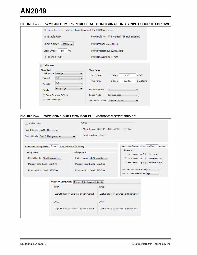
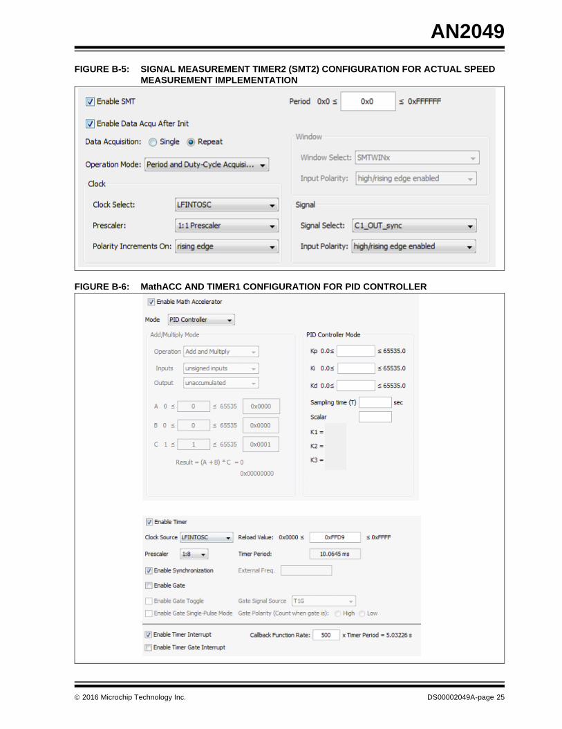
All peripherals used in the firmware are configured andinitialized using the MPLAB® Code Configurator(MCC). Appendix B: “MPLAB® Code Configurator(MCC) Peripheral Initialization” provides the proce-dures on how the peripherals are initialized using MCC.For the complete source code, refer to Appendix C:“Source Code Listing”.
Activate Peek Mode Scanning
Timer4 ISR(Every 600secs)
Do Program Memory Scan
Do CRC Calculation
Mismatch Checksum Value?
RETURN
Shutdown CWG Module
Turn ON Program MemoryLED Indicator
YES
NO
HLT ISR
NOMotor Stall Detected
Shutdown CWG Module
Turn ON Motor Stall LED Indicator
2016 Microchip Technology Inc. DS00002049A-page 19
AN2049
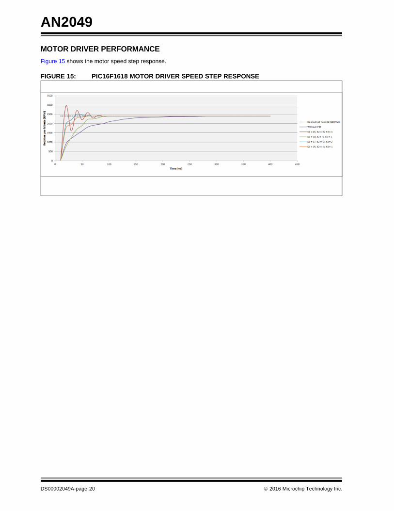
MOTOR DRIVER PERFORMANCE
Figure 15 shows the motor speed step response.
FIGURE 15: PIC16F1618 MOTOR DRIVER SPEED STEP RESPONSE
DS00002049A-page 20 2016 Microchip Technology Inc.
AN2049
CONCLUSION
In cost-sensitive motor control applications, an efficientand flexible microcontroller can have a significant impact.Device efficiency can be measured against the level ofintegrated peripheral optimized to control tasks along withthe number of pins/memory and the size of the package.In addition, ease of use and less time to market areimportant, especially if multiple versions of the designsare required. This application note describes how a low-cost microcontroller meets these requirements. By usingthe PIC16F1618 microcontroller, the motor driver cancontrol the driver switches, set motor speed, predict rotorposition, correct speed error, detect Fault event, andensure program memory data integrity.
2016 Microchip Technology Inc. DS00002049A-page 21
AN2049
APPENDIX A: CIRCUIT SCHEMATIC
FIGURE A-1: SENSORED SINGLE-PHASE BLDC MOTOR DRIVER USING PIC16F1618 SCHEMATIC DIAGRAM CIRCUIT
DS00002049A-page 22 2016 Microchip Technology Inc.
In this section, the MPLAB® Code Configurator (MCC) isutilized to easily configure the peripherals used in thismotor control application. The MCC is a user-friendlyplug-in tool for MPLAB® X IDE which generates drivers
for controlling and driving peripherals of PIC® microcon-trollers, based on the settings and selections made in itsGraphical User Interface (GUI). Refer to the “MPLAB®
Code Configurator User’s Guide” (DS40001725) forfurther information on how to install and set up the MCCin MPLAB X IDE.
The following figures will provide a guide on how toconfigure the PIC16F1618 peripherals in thisapplication note using MCC.
FIGURE B-1: CONFIGURATION REGISTERS SETTINGS
FIGURE B-2: SIGNAL MEASUREMENT TIMER1 (SMT1) CONFIGURATION FOR SPEED REFERENCE IMPLEMENTATION
2016 Microchip Technology Inc. DS00002049A-page 23
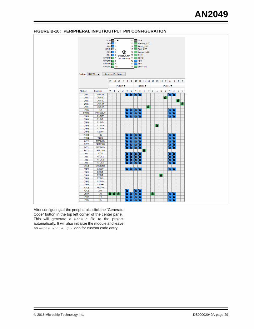
After configuring all the peripherals, click the “GenerateCode” button in the top left corner of the center panel.This will generate a main.c file to the projectautomatically. It will also initialize the module and leavean empty while (1) loop for custom code entry.
2016 Microchip Technology Inc. DS00002049A-page 29
AN2049
APPENDIX C: SOURCE CODE LISTING
The latest software version can be downloaded from theMicrochip web site (www.microchip.com). The user willfind the source code appended to the electronic versionof this application note. The latest version is v3.0.
DS00002049A-page 30 2016 Microchip Technology Inc.
Note the following details of the code protection feature on Microchip devices:
• Microchip products meet the specification contained in their particular Microchip Data Sheet.
• Microchip believes that its family of products is one of the most secure families of its kind on the market today, when used in the intended manner and under normal conditions.
• There are dishonest and possibly illegal methods used to breach the code protection feature. All of these methods, to our knowledge, require using the Microchip products in a manner outside the operating specifications contained in Microchip’s Data Sheets. Most likely, the person doing so is engaged in theft of intellectual property.
• Microchip is willing to work with the customer who is concerned about the integrity of their code.
• Neither Microchip nor any other semiconductor manufacturer can guarantee the security of their code. Code protection does not mean that we are guaranteeing the product as “unbreakable.”
Code protection is constantly evolving. We at Microchip are committed to continuously improving the code protection features of ourproducts. Attempts to break Microchip’s code protection feature may be a violation of the Digital Millennium Copyright Act. If such actsallow unauthorized access to your software or other copyrighted work, you may have a right to sue for relief under that Act.
Information contained in this publication regarding deviceapplications and the like is provided only for your convenienceand may be superseded by updates. It is your responsibility toensure that your application meets with your specifications.MICROCHIP MAKES NO REPRESENTATIONS ORWARRANTIES OF ANY KIND WHETHER EXPRESS ORIMPLIED, WRITTEN OR ORAL, STATUTORY OROTHERWISE, RELATED TO THE INFORMATION,INCLUDING BUT NOT LIMITED TO ITS CONDITION,QUALITY, PERFORMANCE, MERCHANTABILITY ORFITNESS FOR PURPOSE. Microchip disclaims all liabilityarising from this information and its use. Use of Microchipdevices in life support and/or safety applications is entirely atthe buyer’s risk, and the buyer agrees to defend, indemnify andhold harmless Microchip from any and all damages, claims,suits, or expenses resulting from such use. No licenses areconveyed, implicitly or otherwise, under any Microchipintellectual property rights unless otherwise stated.
2016 Microchip Technology Inc.
QUALITY MANAGEMENT SYSTEM CERTIFIED BY DNV
== ISO/TS 16949 ==
Trademarks
The Microchip name and logo, the Microchip logo, dsPIC, FlashFlex, flexPWR, JukeBlox, KEELOQ, KEELOQ logo, Kleer, LANCheck, MediaLB, MOST, MOST logo, MPLAB, OptoLyzer, PIC, PICSTART, PIC32 logo, RightTouch, SpyNIC, SST, SST Logo, SuperFlash and UNI/O are registered trademarks of Microchip Technology Incorporated in the U.S.A. and other countries.
The Embedded Control Solutions Company and mTouch are registered trademarks of Microchip Technology Incorporated in the U.S.A.
Analog-for-the-Digital Age, BodyCom, chipKIT, chipKIT logo, CodeGuard, dsPICDEM, dsPICDEM.net, ECAN, In-Circuit Serial Programming, ICSP, Inter-Chip Connectivity, KleerNet, KleerNet logo, MiWi, motorBench, MPASM, MPF, MPLAB Certified logo, MPLIB, MPLINK, MultiTRAK, NetDetach, Omniscient Code Generation, PICDEM, PICDEM.net, PICkit, PICtail, RightTouch logo, REAL ICE, SQI, Serial Quad I/O, Total Endurance, TSHARC, USBCheck, VariSense, ViewSpan, WiperLock, Wireless DNA, and ZENA are trademarks of Microchip Technology Incorporated in the U.S.A. and other countries.
SQTP is a service mark of Microchip Technology Incorporated in the U.S.A.
Silicon Storage Technology is a registered trademark of Microchip Technology Inc. in other countries.
GestIC is a registered trademark of Microchip Technology Germany II GmbH & Co. KG, a subsidiary of Microchip Technology Inc., in other countries.
All other trademarks mentioned herein are property of their respective companies.
Microchip received ISO/TS-16949:2009 certification for its worldwide
DS00002049A-page 31
headquarters, design and wafer fabrication facilities in Chandler and Tempe, Arizona; Gresham, Oregon and design centers in California and India. The Company’s quality system processes and procedures are for its PIC® MCUs and dsPIC® DSCs, KEELOQ® code hopping devices, Serial EEPROMs, microperipherals, nonvolatile memory and analog products. In addition, Microchip’s quality system for the design and manufacture of development systems is ISO 9001:2000 certified.
DS00002049A-page 32 2016 Microchip Technology Inc.
AMERICASCorporate Office2355 West Chandler Blvd.Chandler, AZ 85224-6199Tel: 480-792-7200 Fax: 480-792-7277Technical Support: http://www.microchip.com/supportWeb Address: www.microchip.com
AtlantaDuluth, GA Tel: 678-957-9614 Fax: 678-957-1455
Austin, TXTel: 512-257-3370
BostonWestborough, MA Tel: 774-760-0087 Fax: 774-760-0088
ChicagoItasca, IL Tel: 630-285-0071 Fax: 630-285-0075