2017 Microchip Technology Inc. DS00002059B-page 1 AN2059 INTRODUCTION LIN (Local Interconnect Network) is a low-cost serial communications protocol implemented mostly in automotive networks. It is typically used for mechatronic nodes in automobiles, but is also well- suited for industrial applications. Users new to LIN communication often struggle with the overhead of the high layers of LIN protocol intricacies (e.g., LDF, NCF files). When in fact, the goal is to simply and quickly evaluate LIN MCUs and LIN PHYs hardware with very basic LIN message transmission. To assist with rapid prototyping, the complimentary MCC LIN Code Generator was created. When your LIN application is ready for production, customizable production-proven LIN Stacks and support are available from Microchip’s LIN design and third party partners. The first part of this application note covers the basics of LIN to provide a brief background on how it works. However, it is highly recommended that the reader is familiar with the LIN specification v2.2A (the most current specification available at the time of this publication). The second part describes a sample demonstration of the LIN protocol using the Microchip MPLAB ® Code Configurator (MCC) LIN Stack Library. The default library supports PIC ® MCUs that have a hardware EUSART peripheral. The latest MCC LIN updates also add support for bit-banged EUART, enhanced checksum and slave automatic bit rate detection using the bit-banged EUART.This document provides step- by-step procedures on how to generate both LIN master and slave drivers quickly and easily. MCC LIN Stack Features The MCC generates code for following basic LIN functions: • Constructs LIN message frame by combining EUART bytes • Automates LIN PID generation with user-defined frame names • Generates LIN classic or enhanced checksum value based on LIN message frame configuration • Generates a scheduler example code showing the use of generated LIN APIs • Supports only unconditional type frame • Allows user-defined frame names • Allows user-defined data length (1 to 8 bytes) • Configurable time out and period down to one millisecond • Supports hardware interrupts • Auto-baud Detection for LIN Slave Nodes using the Bit-Banged EUART LIN BASICS The following sections provide a brief description on the basics of LIN to help readers understand the MCC LIN Stack implementation more easily. LIN Network Configuration A LIN cluster is composed of a single-wire bus, a master node and up to 15 slave nodes. A typical network connection is shown in Figure 1. The master controls the bus activity while the slaves send or receive information depending on the scheduled tasks. Author: Mary Tamar Tan Brian Bailey Han Lin Microchip Technology Inc. Note: The MCC LIN Stack is intended for basic LIN introduction and for prototype purposes only. It is limited to low-level LIN layer to allow the most basic LIN message transmis- sion. Refer to the LIN Stack section for more detail about the limitations. LIN Basics and Implementation of the MCC LIN Stack Library on 8-Bit PIC ® Microcontrollers
Transcript
AN2059LIN Basics and Implementation of the MCC LIN Stack Library
on 8-Bit PIC® Microcontrollers
INTRODUCTIONLIN (Local Interconnect Network) is a low-cost serialcommunications protocol implemented mostly inautomotive networks. It is typically used formechatronic nodes in automobiles, but is also well-suited for industrial applications. Users new to LINcommunication often struggle with the overhead of thehigh layers of LIN protocol intricacies (e.g., LDF, NCFfiles). When in fact, the goal is to simply and quicklyevaluate LIN MCUs and LIN PHYs hardware with verybasic LIN message transmission. To assist with rapidprototyping, the complimentary MCC LIN CodeGenerator was created. When your LIN application isready for production, customizable production-provenLIN Stacks and support are available from Microchip’sLIN design and third party partners.
The first part of this application note covers the basicsof LIN to provide a brief background on how it works.However, it is highly recommended that the reader isfamiliar with the LIN specification v2.2A (the mostcurrent specification available at the time of thispublication).
The second part describes a sample demonstration ofthe LIN protocol using the Microchip MPLAB® CodeConfigurator (MCC) LIN Stack Library. The defaultlibrary supports PIC® MCUs that have a hardwareEUSART peripheral. The latest MCC LIN updates alsoadd support for bit-banged EUART, enhancedchecksum and slave automatic bit rate detection usingthe bit-banged EUART.This document provides step-by-step procedures on how to generate both LINmaster and slave drivers quickly and easily.
MCC LIN Stack FeaturesThe MCC generates code for following basic LINfunctions:
• Constructs LIN message frame by combining EUART bytes
• Automates LIN PID generation with user-defined frame names
• Generates LIN classic or enhanced checksum value based on LIN message frame configuration
• Generates a scheduler example code showing the use of generated LIN APIs
• Supports only unconditional type frame• Allows user-defined frame names• Allows user-defined data length (1 to 8 bytes)• Configurable time out and period down to one
millisecond• Supports hardware interrupts• Auto-baud Detection for LIN Slave Nodes using
the Bit-Banged EUART
LIN BASICSThe following sections provide a brief description onthe basics of LIN to help readers understand the MCCLIN Stack implementation more easily.
LIN Network ConfigurationA LIN cluster is composed of a single-wire bus, amaster node and up to 15 slave nodes. A typicalnetwork connection is shown in Figure 1. The mastercontrols the bus activity while the slaves send orreceive information depending on the scheduled tasks.
Author: Mary Tamar TanBrian BaileyHan LinMicrochip Technology Inc.
Note: The MCC LIN Stack is intended for basicLIN introduction and for prototype purposesonly. It is limited to low-level LIN layer toallow the most basic LIN message transmis-sion. Refer to the LIN Stack section for moredetail about the limitations.
2017 Microchip Technology Inc. DS00002059B-page 1
AN2059
FIGURE 1: LIN NETWORK CONFIGURATION
The MCC LIN Stack, which is the core focus of thisapplication note, provides the interface between thephysical interface and the higher-level applicationfirmware. The EUSART module is the key elementused in LIN communications. It acts as the serialengine for LIN putting serial control in hardware ratherthan in software. Thus, miscellaneous processing canbe done while data is being transmitted or received.The transceiver acts as a bidirectional, half-duplexcommunication physical interface between theEUSART module and the bus. See Section“Electrical Connections” for more informationregarding the LIN physical layer.
Electrical ConnectionsThe LIN bus operates between 9V and 18V. Typically,the microcontroller LIN I/O pins voltage levels areadjusted to the LIN bus levels by a transceiver. Thisallows the microcontrollers to operate at 5V levels,while the bus operates at higher levels. Microchipoffers a portfolio of LIN transceivers, some havingadditional built-in features, such as Internal VoltageRegulator (VREG) and Windowed Watchdog Timer(WWDT). A sample block diagram for a MCP202XALIN transceiver is shown in Figure 2.
Master
TX RX
Transceiver
•••
LIN Bus
EUSART
LIN Protocol Driver
Higher Level
Applications
Slave 1
TX RX
Transceiver
EUSART
LIN Protocol Driver
Higher Level
Applications
Slave 1
TX RX
Transceiver
EUSART
LIN Protocol Driver
Higher Level
Applications
DS00002059B-page 2 2017 Microchip Technology Inc.
AN2059
FIGURE 2: LIN TRANSCEIVER MCP202XA BLOCK DIAGRAM
Refer to www.microchip.com/lin for the complete list ofLIN transceivers from Microchip.
The bus is terminated to VBAT at each node. Themaster should be terminated through a 1 kΩ resistorwhile the slave through a 30 kΩ resistor. As shown inFigure 2, the MCP202XA LIN transceivers alreadyhave an internal 30 kΩ terminating resistor, henceexternal termination for slaves are no longer required.The maximum bus length is designed to be 40 meters.Figure 3 shows a sample LIN physical connection.
Refer to MCP202XA data sheet (DS20002298) for“Typical Application Circuit” at www.microchip.com/MCP2021A.
Frames and SignalsA frame is defined as the entity that is being transferredon the LIN bus. A frame is divided into two parts: theframe header and the frame response. Each serial databyte starts with a Start bit (Dominant signal) and isterminated by a Stop bit (Recessive signal). Whensignal logic is zero, it is called the dominant signal.When signal logic is one, it is called the recessivesignal.
FIGURE 4: FRAME STRUCTURE
The frame header is always sent by the master and itconsists of the Break Field, the Sync Field and theProtected Identifier (PID) Field.
The Break Field consists of at least 13-bit time long ofdominant signal followed by a Break delimiter. TheBreak delimiter is at least one-bit time long of recessivesignal. This is followed by a Sync Field with a datavalue of 0x55. The Break Field sequence enables aslave to identify the beginning of a new frame. TheSync Field allows the slave to synchronize with themaster clock.
The PID field consists of six frame identifier bits andtwo parity bits. The frame ID denotes a uniquemessage address, but does not necessarily define aspecific destination of the message. The MCC LINStack includes an algorithm to automatically calculatethe parity of the frame ID.
The frame response can be from the master itself orany slave. Only the node with the matching IDs willsend the response. The response consists of the DataField and the Checksum Field.
The Data Field is composed of signals. A signal iseither a scalar value or a byte array. A scalar signalcarries value between 1 bit to 16 bits. The byte arraysignal carries value between 1 byte to 8 bytes. A signalis always present at the same position of the data fieldfor all frames with the same frame identifier. It shouldalso be sent by a single publisher, though there are nolimits to the number of subscribers. These signals areused in the higher-level application. A frame is alwaysended by the checksum field. The MCC LIN Stackprovides an option between classic and enhancedchecksum. Classic checksum calculation is performedon the data bytes only. The enhanced checksumcalculation includes both the data bytes and the PID.
The inter-byte space is the time between the end of theStop bit of the previous field and the Start bit of thesucceeding byte. The response space is the timebetween the header and response field. Lastly, inter-frame space is the time between the end of a frame tothe start of a next frame.
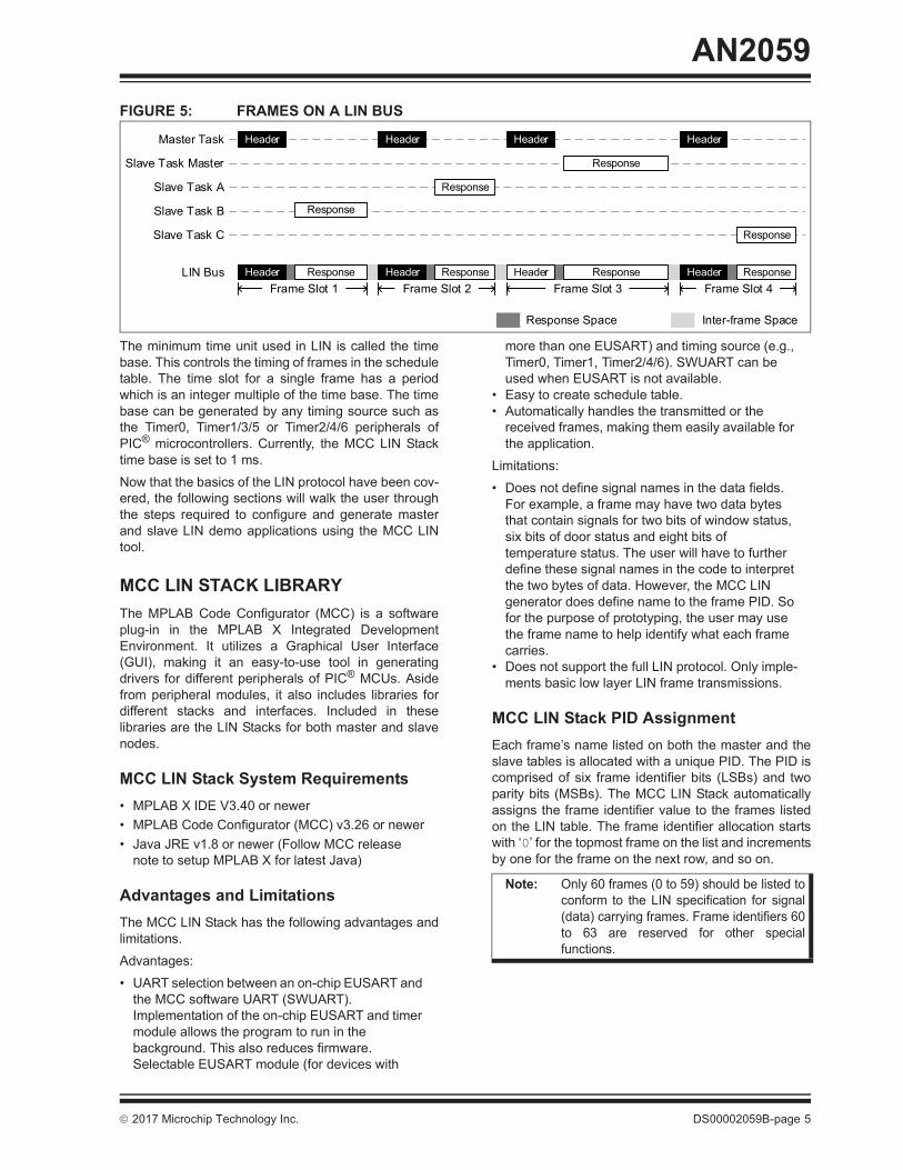
LIN Bus TimingThe transmission and reception in a LIN bus areconsidered to be both deterministic and periodic. Thisrequirement is made possible through the use ofschedule tables. The schedule table lists all the framesthat need to be present on the bus at a predefined timeinterval. This prevents the bus from overloading andalso ensures that each frame is properly transmittedand received. Figure 5 shows a sample transmission offrames with different response publishers. Thesubscribers of the signals packed in these frames canbe any of the nodes connected to the bus.
Break Field SYNC Field PID Field Data Field 1 Data Field 8•••
Checksum
Field
Response Space
Inter-byte Space
Header Response
Frame
Inter-frame Space
DS00002059B-page 4 2017 Microchip Technology Inc.
AN2059
FIGURE 5: FRAMES ON A LIN BUS
The minimum time unit used in LIN is called the timebase. This controls the timing of frames in the scheduletable. The time slot for a single frame has a periodwhich is an integer multiple of the time base. The timebase can be generated by any timing source such asthe Timer0, Timer1/3/5 or Timer2/4/6 peripherals ofPIC® microcontrollers. Currently, the MCC LIN Stacktime base is set to 1 ms.
Now that the basics of the LIN protocol have been cov-ered, the following sections will walk the user throughthe steps required to configure and generate masterand slave LIN demo applications using the MCC LINtool.
MCC LIN STACK LIBRARYThe MPLAB Code Configurator (MCC) is a softwareplug-in in the MPLAB X Integrated DevelopmentEnvironment. It utilizes a Graphical User Interface(GUI), making it an easy-to-use tool in generatingdrivers for different peripherals of PIC® MCUs. Asidefrom peripheral modules, it also includes libraries fordifferent stacks and interfaces. Included in theselibraries are the LIN Stacks for both master and slavenodes.
MCC LIN Stack System Requirements• MPLAB X IDE V3.40 or newer• MPLAB Code Configurator (MCC) v3.26 or newer• Java JRE v1.8 or newer (Follow MCC release
note to setup MPLAB X for latest Java)
Advantages and LimitationsThe MCC LIN Stack has the following advantages andlimitations.
Advantages:
• UART selection between an on-chip EUSART and the MCC software UART (SWUART). Implementation of the on-chip EUSART and timer module allows the program to run in the background. This also reduces firmware. Selectable EUSART module (for devices with
more than one EUSART) and timing source (e.g., Timer0, Timer1, Timer2/4/6). SWUART can be used when EUSART is not available.
• Easy to create schedule table.• Automatically handles the transmitted or the
received frames, making them easily available for the application.
Limitations:
• Does not define signal names in the data fields. For example, a frame may have two data bytes that contain signals for two bits of window status, six bits of door status and eight bits of temperature status. The user will have to further define these signal names in the code to interpret the two bytes of data. However, the MCC LIN generator does define name to the frame PID. So for the purpose of prototyping, the user may use the frame name to help identify what each frame carries.
• Does not support the full LIN protocol. Only imple-ments basic low layer LIN frame transmissions.
MCC LIN Stack PID AssignmentEach frame’s name listed on both the master and theslave tables is allocated with a unique PID. The PID iscomprised of six frame identifier bits (LSBs) and twoparity bits (MSBs). The MCC LIN Stack automaticallyassigns the frame identifier value to the frames listedon the LIN table. The frame identifier allocation startswith ‘0’ for the topmost frame on the list and incrementsby one for the frame on the next row, and so on.
Master Task
Slave Task Master
Slave Task A
Slave Task B
Slave Task C
Header
Response
Header
Response
Header
Response
Header
Response
Header Response Header Response Header Response Header ResponseLIN Bus
Note: Only 60 frames (0 to 59) should be listed toconform to the LIN specification for signal(data) carrying frames. Frame identifiers 60to 63 are reserved for other specialfunctions.
2017 Microchip Technology Inc. DS00002059B-page 5
AN2059
The parity bits P0 and P1 are automatically calculatedby the stack. Alternately, an ID to PID look-up table isprovided in Appendix A: “Frame PID Look-UpTable”. This table can be useful when the user usestesting tools such as LIN Serial Analyzer from Micro-chip. The user can find the corresponding PID valuebased on the frame ID to transmit frames.
Checksum CalculationThe MCC LIN Stack calculates both the classic check-sum used in LIN spec 1.x and the Enhanced Checksumused in LIN spec 2.x. The user can select either check-sum type via the MCC GUI. Both Master and Slavenodes will use the same checksum type.
Classic checksum returns the inverted 8-bit sum withCarry bit value over all of the data bytes in the frame.The enhanced checksum simply adds the PID byte inaddition to the data bytes.
While testing, make sure the LIN analyzer that you usealso selects the corresponding checksum type, other-wise it may misread the frame as error.
Associated PeripheralsAside from the LIN Stack Library, two peripheralmodules also need to be configured. These are theEUSART module for the transmission and thereception of frames and a timer module for the LIN bustime base.
EUSART MODULEThe Enhanced Universal Synchronous AsynchronousReceiver Transmitter (EUSART) module of 8-bit PICmicrocontrollers is a serial communications peripheralthat contains all the clock generators, shift registersand data buffers necessary to perform an input or out-put serial data transfer independent of device programexecution. Besides the basic USART features, themodule exhibits a few capabilities which make it idealfor use in LIN bus systems:
• Automatic detection and calibration of the baud rate• Wake-up on Break reception• 13-bit Break character transmit
To comply with the LIN standard, each charactertransmission should be configured to have one Start bitfollowed by one or up to eight data bytes and alwaysterminated by a Stop bit. The Start bit is always a ‘0’and a Stop bit is always a ‘1’. Each bit persists for aperiod of 1/(baud rate). The Baud Rate Generator(BRG) of the EUSART module automatically derivesthe baud rate from the system oscillator frequency. TheEUSART transmits and receives the LSB first.
Moreover, enabling the EUSART interrupt allows theLIN application program to run in the background whilethe microcontroller is performing other important tasks.This allows the MCU to perform other applications andimprove time and power performance.
TIMER MODULEThe timing source can be selected from the availabletimer modules. Timer1, for example, is a 16-bit timerthat increments on every instruction cycle whenimplemented with no prescaler and generates aninterrupt-on-overflow. Timer2/4/6, on the other hand, isan 8-bit timer which generates an interrupt when amatch between the timer and the period registeroccurs. Selection of timing source depends upon theavailability of the module and the requirements of thespecific application. The selected timer’s period shouldalways be set to 1 ms. This 1 ms time base is used tocontrol the timing of each message frame in a scheduletable.
The step-by-step instructions on how to configure theLIN library, as well as its associated peripherals arecovered in the subsequent sections.
MCC LIN STACK DEMOThe demo programs presented in this application noteuse MCC 3.26. Refer to www.microchip.com/mcc fordetails on how to download and install the latest versionof MCC.
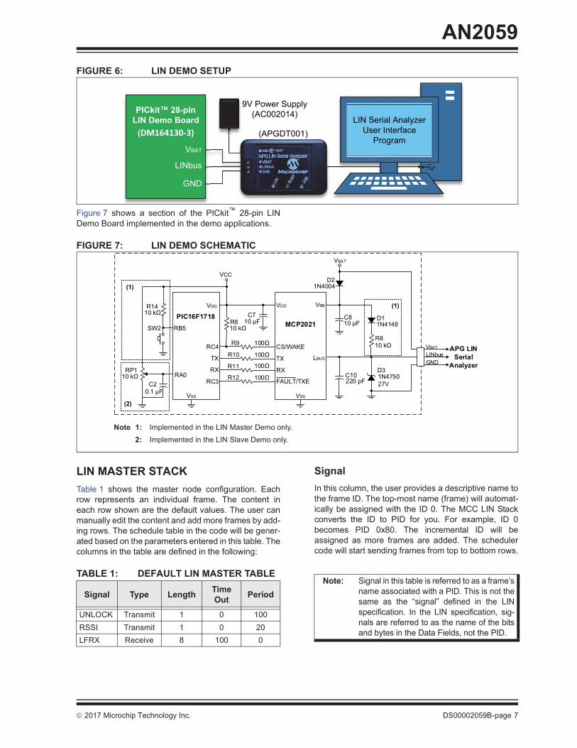
The demo hardware for both the LIN master and theLIN slave stacks make use of the PICkit™ 28-pin LINDemo Board (Part Number DM164130-3) and the LINSerial Analyzer (Part Number APGDT001). A simplifiedsetup is shown in Figure 6.
Note: LIN specification requires Frame identifi-ers 60 (0x3C) to 61 (0x3D) to always useclassic checksum.
Figure 7 shows a section of the PICkit™ 28-pin LINDemo Board implemented in the demo applications.
FIGURE 7: LIN DEMO SCHEMATIC
LIN MASTER STACKTable 1 shows the master node configuration. Eachrow represents an individual frame. The content ineach row shown are the default values. The user canmanually edit the content and add more frames by add-ing rows. The schedule table in the code will be gener-ated based on the parameters entered in this table. Thecolumns in the table are defined in the following:
TABLE 1: DEFAULT LIN MASTER TABLE
SignalIn this column, the user provides a descriptive name tothe frame ID. The top-most name (frame) will automat-ically be assigned with the ID 0. The MCC LIN Stackconverts the ID to PID for you. For example, ID 0becomes PID 0x80. The incremental ID will beassigned as more frames are added. The schedulercode will start sending frames from top to bottom rows.
LIN Serial Analyzer
User Interface
Program
9V Power Supply
(AC002014)
(APGDT001)
LINbus
GND
VBAT
PICkit™ 28-pin LIN Demo Board
(DM164130 3)
PIC16F1718
RC4
TX
RX
RC3
VSS VSS
R9
R10
R11
R12
100Ω
100Ω
100Ω
100Ω
VDD
VCC
R810 kΩ
CS/WAKE
TX
RX
FAULT/TXE
LBUS
RB5
R1410 kΩ
VDD
C710 µF
VBB
VBAT
R810 kΩ
D21N4004
D11N4148
C10220 pF
D31N4750
27V
MCP2021C810 µF
RA0
SW2
C2
0.1 µF
RP110 kΩ
(1)
(1)
(2)
APG LIN Serial
Analyzer
VBAT
LINbus
GND
Note 1: Implemented in the LIN Master Demo only.2: Implemented in the LIN Slave Demo only.
Note: Signal in this table is referred to as a frame’sname associated with a PID. This is not thesame as the “signal” defined in the LINspecification. In the LIN specification, sig-nals are referred to as the name of the bitsand bytes in the Data Fields, not the PID.
2017 Microchip Technology Inc. DS00002059B-page 7
AN2059
TypeThe frame can either be a Transmit or a Receive type.Configuring the frame as Transmit type means that theframe’s data will be from the master. In other words, theresponse will be transmitted from the master itself fol-lowing the header. Configuring the frame as Receivetype means that the frame’s data will be from a slave.In other words, after the master sends out the header,the master is expecting a response from a slave node.
LengthThe length is the number of bytes in the data field. Itshould be a value between 1 to 8.
Time OutTime out is the interval in millisecond (ms) between theend of the frame’s header and the expected time whena node should finish transmitting the response. If anode takes longer than the expected time out tocomplete a response, the master stops transmitting thecurrent frame and moves on to transmitting the nextframe. Make sure the time out is at least longer thanresponse space and the frame’s response combined.Otherwise, the current frame will keep getting skippedand act as if it does not work.
PeriodThe period is the time interval in milliseconds (ms)between the start of the current frame to the start of thenext frame. The period should be longer than theamount of time it takes to transmit the current frame.This allows more inter-frame time to account for thenode to process the previous frame before it is ready totake in the next frame.
IMPLEMENTATION OF THE LIN MASTER STACKThis section presents a simple application of the LINmaster library. A PICkit™ 28-pin LIN Demo Board ispopulated with a PIC16F1718 microcontroller and isconfigured as a master to communicate with a LINSerial Analyzer configured as a slave. See Section“MCC LIN Stack Demo” for the proper hardwaresetup.
In the following demo example, only two unconditionalframes will be entered on the schedule table GUI.
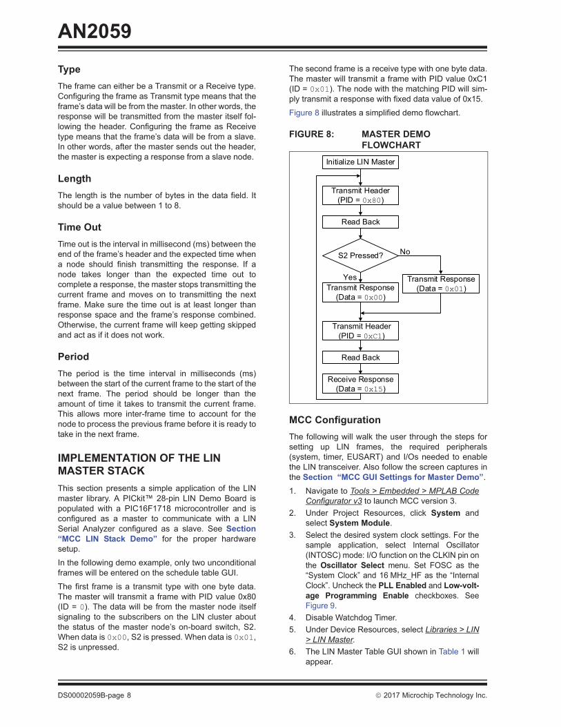
The first frame is a transmit type with one byte data.The master will transmit a frame with PID value 0x80(ID = 0). The data will be from the master node itselfsignaling to the subscribers on the LIN cluster aboutthe status of the master node’s on-board switch, S2.When data is 0x00, S2 is pressed. When data is 0x01,S2 is unpressed.
The second frame is a receive type with one byte data.The master will transmit a frame with PID value 0xC1(ID = 0x01). The node with the matching PID will sim-ply transmit a response with fixed data value of 0x15.
Figure 8 illustrates a simplified demo flowchart.
FIGURE 8: MASTER DEMO FLOWCHART
MCC ConfigurationThe following will walk the user through the steps forsetting up LIN frames, the required peripherals(system, timer, EUSART) and I/Os needed to enablethe LIN transceiver. Also follow the screen captures inthe Section “MCC GUI Settings for Master Demo”.
1. Navigate to Tools > Embedded > MPLAB CodeConfigurator v3 to launch MCC version 3.
2. Under Project Resources, click System andselect System Module.
3. Select the desired system clock settings. For thesample application, select Internal Oscillator(INTOSC) mode: I/O function on the CLKIN pin onthe Oscillator Select menu. Set FOSC as the“System Clock” and 16 MHz_HF as the “InternalClock”. Uncheck the PLL Enabled and Low-volt-age Programming Enable checkboxes. SeeFigure 9.
4. Disable Watchdog Timer.5. Under Device Resources, select Libraries > LIN
> LIN Master.6. The LIN Master Table GUI shown in Table 1 will
appear.
Initialize LIN Master
Transmit Header
(PID = 0x80)
Read Back
S2 Pressed?
Transmit Response
(Data = 0x00)
Transmit Response
(Data = 0x01)
Transmit Header
(PID = 0x )
Read Back
Receive Response
(Data = 0x15)
No
Yes
DS00002059B-page 8 2017 Microchip Technology Inc.
AN2059
7. To add a frame, click Add. An additional row will
appear below the “Signal-Type-Length-Timeout-Period” columns.
8. Edit the fields as shown in Figure 10. Eachcolumn is defined in Section “LIN MasterStack”.
9. Set Checksum Type to Classic and select Tim-er2 as timer. Select EUSART in the EUSARTselection tab.
10. Click the Notifications tab. This tab lists all theadditional configurations that must be done forthe LIN Stack to become fully functional. Takenote of the “HINT” type notification as this will beused later after the MCC settings are generated.
11. One of the notifications describes that the LINmodule uses Timer2. Hence, Timer2 should beconfigured. To do this, navigate to DeviceResources > Peripherals > Timer > TMR2.
12. Check both Enable Timer and Enable TimerInterrupt.
13. Set the Timer Period to 1 ms. When using ahigh-frequency system clock, the prescaler andpostscaler ratios might need some adjustments.
14. Another notification tells that the LIN moduleuses EUSART. Hence, the EUSART moduleneeds to be configured. To do this, navigate toDevice Resources > Peripherals > EUSART >EUSART.
15. In the MCC EUSART GUI, set the mode to asyn-chronous. Check Enable EUSART, EnableTransmit and Enable EUSART Interrupts. Setboth Transmission bits and Reception bits to8-bit, and Clock Polarity to Non-Inverted.
16. Setup the baud rate. The baud rate should be avalue between 1 and 20000. For the sampleapplication, a baud rate of 9600 is used.
17. Set the corresponding EUSART TX and RX pinson the “Pin Manager Grid” at the lower right partof the MCC window. For this example, RC6 andRC7 are assigned as the TX and RX pins,respectively.
18. After setting up both the Timer2 and EUSARTmodules, configure the I/O ports to enable theconnected LIN transceiver (MCP2021). Notethat different transceivers may require differentset up. Refer to the particular transceiver datasheet. For a 28-pin LIN Demo Board, the CS/WAKE and FAULT/TXE pins of the transceiverare connected to the RC4 and RC3 pins,respectively. CS/WAKE should be configured asan output and set high, while FAULT/TXE shouldbe an input with weak pull-ups enabled.
19. Other peripherals can now be configureddepending upon the specific application. For thesample application, only an external switchconnected to RB5 is used. It is configured as adigital input pin. The pin module GUI is shown inFigure 14.
20. Click Generate. When generating the MCCcode for the first time, a pop-up window willappear asking for the configuration settings tobe saved in a .mc3 file format. Enter the desiredfile name then click Save. The configuration set-tings are summarized in Section “MCC GUISettings for Master Demo”.
21. The configuration settings are now generated.However, the configuration process is not yetcomplete. The “HINT” type notification, “AddLIN_handler() in the main.c while loop”should be implemented on the generated code.
22. Uncomment INTERRUPT_GlobalInter-ruptEnable() and INTERRUPT_Peripher-alInterruptEnable() in main.c.
23. The LIN Master driver is now set. For the sampleapplication, the while (1) loop of main.c isshown in Example 1.
EXAMPLE 1: MASTER DEMO CODE SNIPPET
while (1)
// Add your application code
LIN_handler();
if (PORTBbits.RB5 == HIGH)
Master_Switch_Data[0] = 0x01;
else
Master_Switch_Data[0] = 0x00;
2017 Microchip Technology Inc. DS00002059B-page 9
AN2059
MCC GUI Settings for Master DemoThe following figures show the MCC Composer Areaview of the different peripheral modules settingsimplemented in the MCC LIN Stack Master Demo.
FIGURE 9: SYSTEM MODULE SETTINGS
FIGURE 10: LIN MASTER SETTINGS
FIGURE 11: LIN MASTER NOTIFICATIONS
DS00002059B-page 10 2017 Microchip Technology Inc.
AN2059
FIGURE 12: ASSOCIATED MODULE SETTINGS – EUSART
FIGURE 13: ASSOCIATED MODULE SETTINGS – TMR2
2017 Microchip Technology Inc. DS00002059B-page 11
Slave SettingsThe settings for the LIN Serial Analyzer are shown inFigure 15. The implementation of the LIN Serial Ana-lyzer will not be elaborated in this application note.Refer to www.microchip.com for more info.
FIGURE 15: LIN SERIAL ANALYZER SETTINGS
Master Demo ResultsFigure 16 and Figure 17 show the Serial Analyzer andthe Logic Analyzer readings for the master demo appli-cation, respectively. When S2 is pressed (RB5 is low),the master transmits 0x00. Conversely, when S2 is notpressed (RB5 is high), the master transmits 0x01.
DS00002059B-page 12 2017 Microchip Technology Inc.
FIGURE 16: LIN SERIAL ANALYZER DISPLAY FOR MASTER DEMO
Switc
h is
Pr
esse
dSw
itch
is N
ot
Pres
sed
2017 Microchip Technology Inc. DS00002059B-page 13
AN2059
FIGURE 17: LOGIC ANALYZER DISPLAY FOR MASTER DEMO
LIN SLAVE STACKThe default slave node is shown in Table 2. Unlike themaster table, the slave table is only composed of threecolumns for signal, type and length.
TABLE 2: DEFAULT LIN SLAVE TABLE
Master_Switch Frame(Switch Not Pressed: Data = 0x01)
Master_Switch Frame(Switch Pressed: Data = 0x00)
Serial_Analyzer Frame(Slave Response Data = 0x15)
Communication Matrix
Signal Type Length
UNLOCK Receive 1RSSI Receive 1LFRX Transmit 8
DS00002059B-page 14 2017 Microchip Technology Inc.
AN2059
SignalIf the MCC LIN master stack is implemented on themaster node connected on the same bus with thisslave, all the frames listed in the master table shouldalso be entered in the same order on the LIN slavetable. This is due to the PID assignment system imple-mented in the MCC LIN Stack. Using a different mastermay not require this but the user should take note of thespecific PID for the given frame (see Section “MCCLIN Stack PID Assignment”).
TypeConfiguring the frame as Transmit type means theslave is going to transmit the response after receivingthe header with the matching PID from the master.Configuring frame as Receive type means the slave isa subscriber to the data in the Data Field of the corre-sponding frame (PID).
LengthThe length is the number of bytes in a frame’s datafield. The length should be the same on both masternode or slave nodes for a corresponding frame PID.For example, if PID 0x80 frame has length of two databytes, so should the slave.
IMPLEMENTATION OF THE LIN SLAVE STACKThis section presents a sample application of the MCCLIN slave driver using a LIN Serial Analyzer as themaster and a PICkit™ 28-pin LIN Demo Board popu-lated with a PIC16F1718 microcontroller as slave. Thisdemo makes use of the on-board potentiometer RP1and the on-chip Analog-to-Digital Converter (ADC)module of the PIC16F1718. See Section “MCC LINStack Demo” for the hardware setup.
A simplified flowchart for the slave demo is shown inFigure 18. The slave will only transmit a response if aPID of 0xC1 is received. It will send a data byte with avalue equal to the eight LSBs of the ADC reading of thepotentiometer input.
FIGURE 18: SLAVE DEMO FLOWCHART
MCC ConfigurationTo configure the MCC LIN slave driver, follow thesesteps:
1. Navigate to Tools > Embedded > MPLAB CodeConfigurator v3 to launch MCC version 3.
2. Under “Project Resources”, click System andselect System Module.
3. Select the desired system clock settings. For thesample application, select Internal Oscillator(INTOSC) mode: I/O function on the CLKIN pin onthe Oscillator Select menu. Set FOSC as the“System Clock” and 16 MHz_HF as the “InternalClock.” Uncheck the PLL Enabled and Low-volt-age Programming Enable checkboxes. SeeFigure 9.
4. Disable Watchdog Timer.5. Under “Device Resources”, select Libraries >
LIN > LIN Slave.6. The LIN Slave Table GUI shown in Table 2 will
appear.7. To add a frame, click the Easy Setup tab then
Add. An additional row will appear below the“Signal-Type-Length” columns.
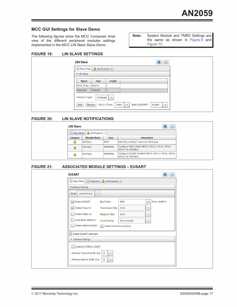
8. Edit the fields as shown in Figure 19. Each columnis defined in Section “LIN Slave Stack”.
9. Set Checksum Type to Enhanced and selectTimer2 as timer. Select EUSART in the EUSARTselection tab.
Note: In a LIN cluster, we may have multiplesubscribers (receivers or listeners) to amaster’s frame. However, only oneresponse to a frame header (only onepublisher) is allowed at a given time. Forexample, if the master configures frameID 0 to be a transmit type, it is allowed tohave multiple slave nodes to have thesame frame ID 0 to be as receive type. Inanother example, if the master configuresframe ID 0 to be a receive type, only oneslave node is allowed to configure astransmit type to respond to the frame ID 0.
Initialize LIN Slave
PID = 0xC1?
Transmit Response
(Data = ADRESL)
No
Yes
Receive Header
ADC of RP1
Channel
2017 Microchip Technology Inc. DS00002059B-page 15
AN2059
10. Click the Notifications tab. This tab lists all the
additional configurations that must be done forthe LIN Stack to become fully functional. Takenote of the “HINT” type notification, as this willbe used later after the MCC settings are gener-ated.
11. One of the notifications describes that the LINmodule uses Timer2. Hence, Timer2 should beconfigured. To do this, navigate to DeviceResources > Peripherals > Timer > TMR2.
12. Check both Enable Timer and Enable TimerInterrupt.
13. Set the Timer Period to 1 ms. When using highfrequency system clock, the prescaler and post-scaler ratios might need some adjustments.
14. Another notification tells that the LIN moduleuses EUSART. Hence, the EUSART moduleneeds to be configured. To do this, navigate toDevice Resources > Peripherals > EUSART >EUSART [PIC10 / PIC12 / PIC16 / PIC18 MCUsby Microchip Technology, Inc.].
15. In the MCC EUSART GUI, set the mode to asyn-chronous. Check Enable EUSART, EnableTransmit, Enable Continuous Receive andEnable EUSART Interrupts. Set both Trans-mission bits and Reception bits to 8-bit, andClock Polarity to Non-Inverted.
16. Setup the baud rate. The baud rate should be avalue between 1 and 20000. For the sampleapplication, a baud rate of 9600 is used.
17. Set the corresponding EUSART TX and RX pinson the “Pin Manager Grid” at the lower right part ofthe MCC window. For this example, RC6 and RC7are assigned as the TX and RX pins, respectively.
18. After setting up both the Timer2 and EUSARTmodules, configure the I/O ports to enable theconnected LIN transceiver (MCP2021). Notethat different transceivers may require differentsetup. Refer to the particular transceiver data
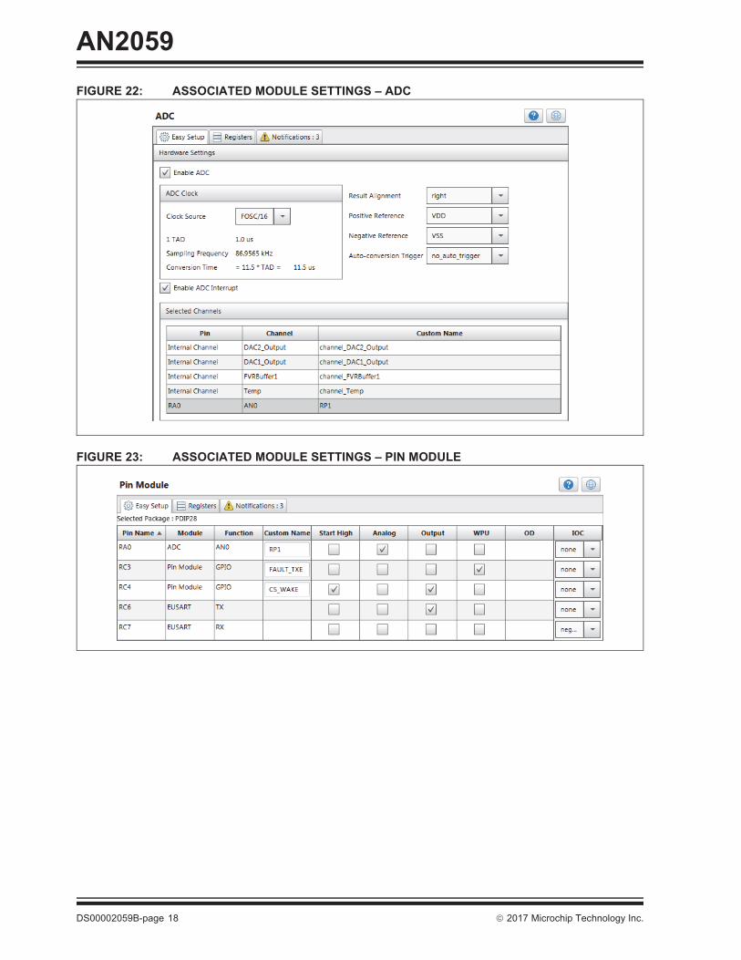
sheet. For a 28-pin LIN Demo Board, the CS/WAKE and FAULT/TXE pins of the transceiverare connected to RC4 and RC3, respectively.CS/WAKE should be configured as an outputand set high, while FAULT/TXE should be aninput with weak pull-ups enabled. The pin mod-ule GUI is shown in Figure 23.
19. Other peripherals can now be configureddepending upon the specific application. Thesample application uses an analog input; there-fore, the ADC module must be setup.
20. To configure the ADC, go to Device Resources> Peripherals > ADC > ADC [PIC10 / PIC12 /PIC16 / PIC18 MCUs by Microchip Technology,Inc.]. In “Table View”, select RA0 as an ADCInput pin. AN0 will then be added automaticallyto the “Selected Channels” list in the “ComposerArea”. Use “RP1” as a custom name for thischannel. Figure 22 details the complete ADCsettings.
21. Click Generate. When generating the MCCcode for the first time, a pop-up window willappear asking for the configuration settings tobe saved in a .mc3 file format. Enter the desiredfile name then click Save. The configuration set-tings are summarized in Section “MCC GUISettings for Slave Demo”.
22. The configuration settings are now generated.However, the configuration process is not yetcomplete. The “HINT” type notification, “AddLIN_handler() in the main.c while loop”,should be implemented on the generated code.
23. Uncomment INTERRUPT_GlobalInter-ruptEnable() and INTERRUPT_Peripher-alInterruptEnable() in main.c.
24. The LIN Slave driver is now set. For the sampleapplication, ../adc.h should be included inlin_app.c, and processLIN() is modifiedas shown in Example 2.
EXAMPLE 2: SLAVE DEMO CODE SNIPPETvoid processLIN(void)
uint8_t tempRxData[8];
uint8_t cmd;
cmd = LIN_getPacket(tempRxData);
switch(cmd)
case Serial_Analyzer:
break;
case Slave_Pot:
Slave_Pot_Data[0] = ADC_GetConversion(RP1);
break;
default:
break;
DS00002059B-page 16 2017 Microchip Technology Inc.
AN2059
MCC GUI Settings for Slave DemoThe following figures show the MCC Composer Areaview of the different peripheral modules settingsimplemented in the MCC LIN Stack Slave Demo.
FIGURE 19: LIN SLAVE SETTINGS
FIGURE 20: LIN SLAVE NOTIFICATIONS
FIGURE 21: ASSOCIATED MODULE SETTINGS – EUSART
Note: System Module and TMR2 Settings arethe same as shown in Figure 9 andFigure 13.
2017 Microchip Technology Inc. DS00002059B-page 17
DS00002059B-page 18 2017 Microchip Technology Inc.
AN2059
Slave Demo ResultsFigure 24 and Figure 25 show the Serial Analyzer andthe Logic Analyzer readings for the slave demo,respectively. The master periodically sends data with ahex value of 0x07, while the slave responds with theeight LSBs of the ADC reading from the potentiometerinput every time the PID of 0xC1 is broadcasted by themaster.
FIGURE 24: LIN SERIAL ANALYZER DISPLAY FOR SLAVE DEMO
2017 Microchip Technology Inc. DS00002059B-page 19
AN2059
FIGURE 25: LOGIC ANALYZER DISPLAY FOR SLAVE DEMO
Slave_Pot Frame(Data = ADRESL)
Serial_Analyzer Frame(Master Transmit Data = 0x07)
Communication Matrix
DS00002059B-page 20 2017 Microchip Technology Inc.
AN2059
SWUART IMPLEMENTATIONThis section provides information on how to implementthe SWUART (bit-banged EUART or software EUART)module in MCC as serial engine for both the LIN Masterand slave drivers. The SWUART is an option whenhardware EUART is not available. The SWUART mod-ule is included in the Foundation Services Library thatcan be downloaded from the Microchip website. Thedriver described here is discussed in detail in AN2290“Bit-Banged Enhanced UART for 8-bit PIC® Microcon-trollers”.
Using the MCC SWUART ModuleMCC configuration is almost similar with the examplesshown in the previous sections. The only differencesare:
• SWUART is selected instead of the hardware EUSART module
• TMR0 is used for bit timing. When using SWUART, TMR0 is not allowed to be used as LIN Master/Slave timing source.
The steps presented here are applicable to both theMCC LIN Master and LIN Slave projects. To implementthe SWUART in the previous examples, the followingchanges should be made in the MCC Configurationsteps presented earlier.
1. Select SWUART as the EUSART in the LINMaster or Slave module GUI, as shown inFigure 26.
2. Skip all steps related to EUSART and pin mod-ule configuration (steps 14 to 18 on both the LINMaster and Slave demos). Instead, continuewith the steps shown here.
3. Navigate to Device Resources Libraries Foundation Services SWUART. SelectTMR0 as timer. Set baud rate to 9600, Transmitbuffer size to 8 and Receive buffer size to 8. Itcan be observed that the actual baud rate isequal to 0.0 b/s. To set the actual baud rate,TMR0 should be configured with the requiredtimer period of 104.17 us.
4. To configure TMR0, go to Device Resources Peripherals Timer TMR0
5. Set Clock Source to FOSC/4. To achieve thedesired timer period, check Enable Prescalerand set to 1:2. Set the Requested Period to104.17 us. The actual period should be 104 us,which is the nearest possible value due to inte-ger arithmetic truncation (see Figure 27).
FIGURE 26: SELECTING THE SWUART
6. Go to “Project Resources” and select Pin Module.7. Edit the Pin Module GUI, as shown in Figure 28.
2017 Microchip Technology Inc. DS00002059B-page 21
AN2059
FIGURE 27: TMR0 SETTINGS FOR SWUART IMPLEMENTATION
FIGURE 28: PIN MODULE SETTINGS FOR SWUART IMPLEMENTATION
8. When using the SWUART, make sure that thePreemptive interrupt routine checkbox ischecked and the interrupt priority order is thesame with the one shown in Figure 29. To verify,go to Project Resources Interrupt Module.
FIGURE 29: INTERRUPT MODULE SETTINGS FOR SWUART IMPLEMENTATION
DS00002059B-page 22 2017 Microchip Technology Inc.
AN2059
9. Continue with Step 19 presented in the LIN
Master demo or LIN Slave demo.10. The driver is now set. The application should
give results similar to the examples presentedusing the hardware EUSART.
AUTO-BAUD IMPLEMENTATIONAutomatic detection and calibration of bit rates in LINSlave nodes is performed by timing the period of thereceived Sync character (55h or ASCII “U”). Theunique feature of this character is that it has five risingedges including the Stop bit edge. Both the hardwareEUSART and bit-banged EUART support auto-bauddetection and calibration.
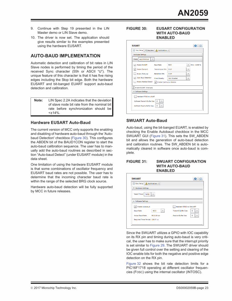
Hardware EUSART Auto-BaudThe current version of MCC only supports the enablingand disabling of hardware auto-baud through the 'Auto-baud Detection' checkbox (Figure 30). This configuresthe ABDEN bit of the BAUD1CON register to start theauto-baud calibration sequence. The user has to man-ually add the auto-baud routines as described in sec-tion “Auto-baud Detect” (under EUSART module) in thedata sheet.
One limitation of using the hardware EUSART moduleis that some combinations of oscillator frequency andEUSART baud rates are not possible. The user has todetermine that the incoming character baud rate iswithin the range of the selected BRG clock source.
Hardware auto-baud detection will be fully supportedby MCC in future releases.
FIGURE 30: EUSART CONFIGURATION WITH AUTO-BAUD ENABLED
SWUART Auto-BaudAuto-baud, using the bit-banged EUART, is enabled bychecking the Enable Autobaud checkbox in the MCCSWUART GUI (Figure 31). This sets the SW_ABDENbit and allows the generation of auto-baud detectionand calibration routines. The SW_ABDEN bit is auto-matically cleared in software once auto-baud is com-plete.
FIGURE 31: SWUART CONFIGURATION WITH AUTO-BAUD ENABLED
Since the SWUART utilizes a GPIO with IOC capabilityon its RX pin and timing during auto-baud is very criti-cal, the user has to make sure that the interrupt priorityis set similar to Figure 29. The SWUART driver shouldbe given full control over the setting and clearing of theIOC enable bits for both the negative and positive edgedetection on the RX pin.
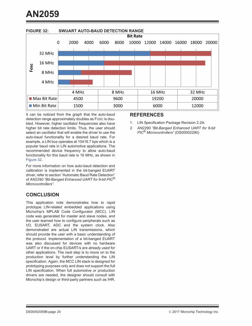
Figure 32 shows the bit rate detection limits for aPIC16F1718 operating at different oscillator frequen-cies (FOSC) using the internal oscillator (INTOSC).
Note: LIN Spec 2.2A indicates that the deviationof slave node bit rate from the nominal bitrate before synchronization should be<±14%.
2017 Microchip Technology Inc. DS00002059B-page 23
AN2059
FIGURE 32: SWUART AUTO-BAUD DETECTION RANGE
It can be noticed from the graph that the auto-bauddetection range approximately doubles as FOSC is dou-bled. However, higher oscillator frequencies also havehigher bit rate detection limits. Thus, the user shouldselect an oscillator that will enable the driver to use theauto-baud functionality for a desired baud rate. Forexample, a LIN bus operates at 10416.7 bps which is apopular baud rate in LIN automotive applications. Therecommended device frequency to allow auto-baudfunctionality for this baud rate is 16 MHz, as shown inFigure 32.
For more information on how auto-baud detection andcalibration is implemented in the bit-banged EUARTdriver, refer to section “Automatic Baud Rate Detection”of AN2290 “Bit-Banged Enhanced UART for 8-bit PIC®
Microcontrollers”.
CONCLUSIONThis application note demonstrates how to rapidprototype LIN-related embedded applications usingMicrochip’s MPLAB Code Configurator (MCC). LINcode was generated for master and slave nodes, andthe user learned how to configure peripherals such asI/O, EUSART, ADC and the system clock. Alsodemonstrated are actual LIN transmissions, whichshould provide the user with a basic understanding ofthe protocol. Implementation of a bit-banged EUARTwas also discussed for devices with no hardwareUART or if the on-chip EUSART/s are already used forother applications. The next step is to move on to theproduction level by further understanding the LINspecification. Again, the MCC LIN stack is designed forprototyping purposes only and does not support the fullLIN specification. When full automotive or productiondrivers are needed, the designer should consult withMicrochip’s design or third-party partners such as IHR.
REFERENCES1. LIN Specification Package Revision 2.2A.2. AN2290 “Bit-Banged Enhanced UART for 8-bit
DS00002059B-page 26 2017 Microchip Technology Inc.
Note the following details of the code protection feature on Microchip devices:• Microchip products meet the specification contained in their particular Microchip Data Sheet.
• Microchip believes that its family of products is one of the most secure families of its kind on the market today, when used in the intended manner and under normal conditions.
• There are dishonest and possibly illegal methods used to breach the code protection feature. All of these methods, to our knowledge, require using the Microchip products in a manner outside the operating specifications contained in Microchip’s Data Sheets. Most likely, the person doing so is engaged in theft of intellectual property.
• Microchip is willing to work with the customer who is concerned about the integrity of their code.
• Neither Microchip nor any other semiconductor manufacturer can guarantee the security of their code. Code protection does not mean that we are guaranteeing the product as “unbreakable.”
Code protection is constantly evolving. We at Microchip are committed to continuously improving the code protection features of ourproducts. Attempts to break Microchip’s code protection feature may be a violation of the Digital Millennium Copyright Act. If such actsallow unauthorized access to your software or other copyrighted work, you may have a right to sue for relief under that Act.
Information contained in this publication regarding deviceapplications and the like is provided only for your convenienceand may be superseded by updates. It is your responsibility toensure that your application meets with your specifications.MICROCHIP MAKES NO REPRESENTATIONS ORWARRANTIES OF ANY KIND WHETHER EXPRESS ORIMPLIED, WRITTEN OR ORAL, STATUTORY OROTHERWISE, RELATED TO THE INFORMATION,INCLUDING BUT NOT LIMITED TO ITS CONDITION,QUALITY, PERFORMANCE, MERCHANTABILITY ORFITNESS FOR PURPOSE. Microchip disclaims all liabilityarising from this information and its use. Use of Microchipdevices in life support and/or safety applications is entirely atthe buyer’s risk, and the buyer agrees to defend, indemnify andhold harmless Microchip from any and all damages, claims,suits, or expenses resulting from such use. No licenses areconveyed, implicitly or otherwise, under any Microchipintellectual property rights unless otherwise stated.
2017 Microchip Technology Inc.
Microchip received ISO/TS-16949:2009 certification for its worldwide headquarters, design and wafer fabrication facilities in Chandler and Tempe, Arizona; Gresham, Oregon and design centers in California and India. The Company’s quality system processes and procedures are for its PIC® MCUs and dsPIC® DSCs, KEELOQ® code hopping devices, Serial EEPROMs, microperipherals, nonvolatile memory and analog products. In addition, Microchip’s quality system for the design and manufacture of development systems is ISO 9001:2000 certified.
QUALITY MANAGEMENT SYSTEM CERTIFIED BY DNV
== ISO/TS 16949 ==
TrademarksThe Microchip name and logo, the Microchip logo, AnyRate, AVR, AVR logo, AVR Freaks, BeaconThings, BitCloud, chipKIT, chipKIT logo, CryptoMemory, CryptoRF, dsPIC, FlashFlex, flexPWR, Heldo, JukeBlox, KEELOQ, KEELOQ logo, Kleer, LANCheck, LINK MD, maXStylus, maXTouch, MediaLB, megaAVR, MOST, MOST logo, MPLAB, OptoLyzer, PIC, picoPower, PICSTART, PIC32 logo, Prochip Designer, QTouch, RightTouch, SAM-BA, SpyNIC, SST, SST Logo, SuperFlash, tinyAVR, UNI/O, and XMEGA are registered trademarks of Microchip Technology Incorporated in the U.S.A. and other countries.
ClockWorks, The Embedded Control Solutions Company, EtherSynch, Hyper Speed Control, HyperLight Load, IntelliMOS, mTouch, Precision Edge, and Quiet-Wire are registered trademarks of Microchip Technology Incorporated in the U.S.A.
Adjacent Key Suppression, AKS, Analog-for-the-Digital Age, Any Capacitor, AnyIn, AnyOut, BodyCom, CodeGuard, CryptoAuthentication, CryptoCompanion, CryptoController, dsPICDEM, dsPICDEM.net, Dynamic Average Matching, DAM, ECAN, EtherGREEN, In-Circuit Serial Programming, ICSP, Inter-Chip Connectivity, JitterBlocker, KleerNet, KleerNet logo, Mindi, MiWi, motorBench, MPASM, MPF, MPLAB Certified logo, MPLIB, MPLINK, MultiTRAK, NetDetach, Omniscient Code Generation, PICDEM, PICDEM.net, PICkit, PICtail, PureSilicon, QMatrix, RightTouch logo, REAL ICE, Ripple Blocker, SAM-ICE, Serial Quad I/O, SMART-I.S., SQI, SuperSwitcher, SuperSwitcher II, Total Endurance, TSHARC, USBCheck, VariSense, ViewSpan, WiperLock, Wireless DNA, and ZENA are trademarks of Microchip Technology Incorporated in the U.S.A. and other countries.
SQTP is a service mark of Microchip Technology Incorporated in the U.S.A.
Silicon Storage Technology is a registered trademark of Microchip Technology Inc. in other countries.
GestIC is a registered trademark of Microchip Technology Germany II GmbH & Co. KG, a subsidiary of Microchip Technology Inc., in other countries.
All other trademarks mentioned herein are property of their respective companies.