2016 Microchip Technology Inc. DS00002080A-page 1 AN2080 INTRODUCTION This application note provides a 230V AC off-line LED driver, three steps dimming solution with load-side short-circuit protection using the HV9805 device. Based on a boost topology with power factor correction (PFC) and output overvoltage protection (OVP) fol- lowed by a linear output current regulator, this solution also offers soft enable-disable control. HV9805 DEVICE GENERAL DESCRIPTION The HV9805 driver integrated circuit (IC) is targeted at general LED lighting products, such as LED lamps and LED lighting fixtures with a maximum power rating of about 25W at 120V AC and 50W at 230V AC . A two-stage topology provides true constant current drive for the LED load while drawing mains power with high power factor. The first stage, a boundary conduc- tion mode boost converter, transfers power from the AC line to a second stage linear current regulator with high power factor and high efficiency. The linear current regulator, arranged for operation with low overhead voltage, transfers power from the first stage to the LED load with true constant current (no ripple) and protects the LED load from the overvoltage that may pass from mains to the output of the first stage. The IC is particularly geared to drive a high voltage LED load. An LED load arranged as a high-voltage load is capable of offering cost advantages in terms of heat management and optics. The boost converter employs a cascode switch for high-speed switching and conve- nient generation of the V DD supply. The control device of the cascode switch is an integral part of the HV9805 and is rated at 700 mA peak. Current for powering the V DD supply is derived by means of an internal connec- tion to the cascode switch. The main characteristics and features of the HV9805 LED driver include a two Stage Driver Topology: •1 st Stage with: - Boundary Conduction Mode (BCM) boost with power factor correction - High power factor (0.98 typical) - High efficiency (90% typical) - Simple V DD supply: no auxiliary winding required - Boost converter cascode switch: internal switch rated at 700 mA peak - Supports up to 25W at 120V AC - Supports up to 50W at 230V AC •2 nd Stage: - Linear post-regulator with low overhead voltage - Zero LED current and brightness ripple - Provides true DC light and protects load from line voltage transients - Output load open circuit protection - High efficiency - ±4% reference over temperature Applications: - LED Lamps - LED Lighting Fixtures - Low Output Voltage Applications, SEPIC Topology Author: Sergiu August Gheorghe Microchip Technology Inc. Note: For the complete list of characteristics, refer to the HV9805 Data Sheet. 230V AC Off-line LED Driver with Dimming and Short-Circuit Load Protection using the HV9805 Controller
Transcript
AN2080230VAC Off-line LED Driver with Dimming and Short-Circuit Load Protection
using the HV9805 Controller
INTRODUCTION
This application note provides a 230VAC off-line LEDdriver, three steps dimming solution with load-sideshort-circuit protection using the HV9805 device.Based on a boost topology with power factor correction(PFC) and output overvoltage protection (OVP) fol-lowed by a linear output current regulator, this solutionalso offers soft enable-disable control.
HV9805 DEVICE GENERAL DESCRIPTION
The HV9805 driver integrated circuit (IC) is targeted atgeneral LED lighting products, such as LED lamps andLED lighting fixtures with a maximum power rating ofabout 25W at 120VAC and 50W at 230VAC.
A two-stage topology provides true constant currentdrive for the LED load while drawing mains power withhigh power factor. The first stage, a boundary conduc-tion mode boost converter, transfers power from theAC line to a second stage linear current regulator withhigh power factor and high efficiency. The linear currentregulator, arranged for operation with low overheadvoltage, transfers power from the first stage to the LEDload with true constant current (no ripple) and protectsthe LED load from the overvoltage that may pass frommains to the output of the first stage.
The IC is particularly geared to drive a high voltageLED load. An LED load arranged as a high-voltage loadis capable of offering cost advantages in terms of heatmanagement and optics. The boost converter employsa cascode switch for high-speed switching and conve-nient generation of the VDD supply. The control deviceof the cascode switch is an integral part of the HV9805and is rated at 700 mA peak. Current for powering theVDD supply is derived by means of an internal connec-tion to the cascode switch.
The main characteristics and features of the HV9805LED driver include a two Stage Driver Topology:
• 1st Stage with:
- Boundary Conduction Mode (BCM) boost with power factor correction
- High power factor (0.98 typical)
- High efficiency (90% typical)
- Simple VDD supply: no auxiliary winding required
- Boost converter cascode switch: internal switch rated at 700 mA peak
- Supports up to 25W at 120VAC
- Supports up to 50W at 230VAC
• 2nd Stage:
- Linear post-regulator with low overhead voltage
- Zero LED current and brightness ripple
- Provides true DC light and protects load from line voltage transients
- Output load open circuit protection
- High efficiency
- ±4% reference over temperature
Applications:
- LED Lamps
- LED Lighting Fixtures
- Low Output Voltage Applications, SEPIC Topology
Author: Sergiu August GheorgheMicrochip Technology Inc.
Note: For the complete list of characteristics,refer to the HV9805 Data Sheet.
For the boost application, the design parameters canbe observed in Table 1.
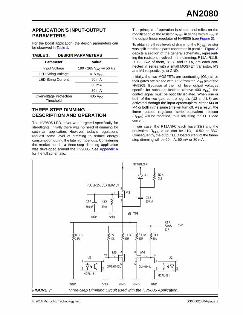
THREE-STEP DIMMING – DESCRIPTION AND OPERATION
The HV9805 LED driver was targeted specifically forstreetlights. Initially there was no need of dimming forsuch an application. However, today’s regulationsrequest some level of dimming to reduce energyconsumption during the late night periods. Consideringthe market needs, a three-step dimming applicationwas developed around the HV9805. See Appendix Afor the full schematic.
The principle of operation is simple and relies on themodification of the resistor RCRS in series with MCRX inthe output linear regulator of HV9805 (see Figure 2).
To obtain the three levels of dimming, the RCRS resistorwas split into three parts connected in parallel. Figure 3depicts a section of the general schematic, represent-ing the resistors involved in the dimming: R11A, R11B,R11C. Two of them, R11C and R11A, are each con-nected in series with a small MOSFET transistor, M3and M4 respectively, to GND.
Initially, the two MOSFETs are conducting (ON) sincetheir gates are biased with 7.5V from the VDD pin of theHV9805. Because of the high level output voltagesspecific for such applications (above 400 VDC), thecontrol signal must be optically isolated. When one orboth of the two gate control signals (U2 and U3) areactivated through the input optocouplers, either M3 orM4 or both in the same time will turn off. As a result, thelinear output regulator series-equivalent resistor(RCRS) will be modified, thus adjusting the LED loadcurrent.
In our case, the R11A/B/C each have 33 and theequivalent RCRS value can be 11, 16.5 or 33.Consequently, the output LED load current of the three-step dimming will be 90 mA, 60 mA or 30 mA.
FIGURE 3: Three-Step Dimming Circuit used with the HV9805 Application.
TABLE 1: DESIGN PARAMETERS
Parameter Value
Input Voltage 190 - 265 VAC @ 50 Hz
LED String Voltage 415 VDC
LED String Current 90 mA
60 mA
30 mA
Overvoltage Protection Threshold
435 VDC
GND GND GND
33RR11A
33RR11B
TP8
33RR11C
VDD
U2U3
33R
R17
21
3
IPD65R250C6XTMA1CT
M2
330kR25
GND
560 pFC14
GND
2k2R26
220 pFC13
10kR9
10kR11
STTH1L06A
D3
DG
S
M4
DMN6140L
DG
S
M3
DMN6140L 23
14
HCPL-181
U2
GND
2 3
1 4
HCPL-181
U3
GND
2016 Microchip Technology Inc. DS00002080A-page 3
AN2080
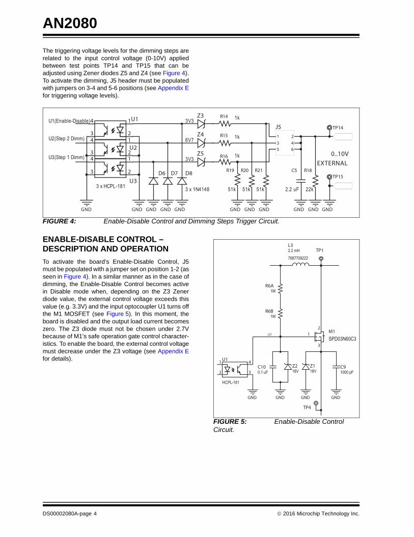
The triggering voltage levels for the dimming steps arerelated to the input control voltage (0-10V) appliedbetween test points TP14 and TP15 that can beadjusted using Zener diodes Z5 and Z4 (see Figure 4).To activate the dimming, J5 header must be populatedwith jumpers on 3-4 and 5-6 positions (see Appendix Efor triggering voltage levels).
FIGURE 4: Enable-Disable Control and Dimming Steps Trigger Circuit.
ENABLE-DISABLE CONTROL – DESCRIPTION AND OPERATION
To activate the board’s Enable-Disable Control, J5must be populated with a jumper set on position 1-2 (asseen in Figure 4). In a similar manner as in the case ofdimming, the Enable-Disable Control becomes activein Disable mode when, depending on the Z3 Zenerdiode value, the external control voltage exceeds thisvalue (e.g. 3.3V) and the input optocoupler U1 turns offthe M1 MOSFET (see Figure 5). In this moment, theboard is disabled and the output load current becomeszero. The Z3 diode must not be chosen under 2.7Vbecause of M1’s safe operation gate control character-istics. To enable the board, the external control voltagemust decrease under the Z3 voltage (see Appendix Efor details).
FIGURE 5: Enable-Disable Control Circuit.
23
14
U3
GND GND
23
14U2
23
14
3 x HCPL-181
U1U1(Enable-Disable)
U2(Step 2 Dimm)
U3(Step 1 Dimm)
1kR15
1kR16
1kR14
TP14
TP15
GND
D6 D7
GND
2.2 uF
C5
GND
3 x 1N4148
D8
GND
22k
R18
GND
11 23 45 6
J5
51k
R19
51k
R20
51k
R21
GND GND GND GND
3V3Z3
6V7Z4
3V3Z5 0..10V
EXTERNAL
21
3SPD03N60C3M1
1MR6A
1MR6B
18VZ2
0.1 uFC10
GND
TP1
TP4
18VZ1
GND
2.2 mH7687709222
L3
U1
1000 pFC9
GND
2 3
1 4
HCPL-181
U1
GND
DS00002080A-page 4 2016 Microchip Technology Inc.
AN2080
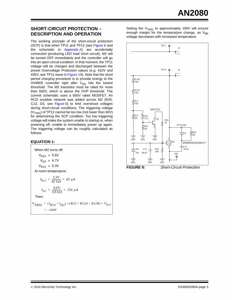
SHORT-CIRCUIT PROTECTION – DESCRIPTION AND OPERATION
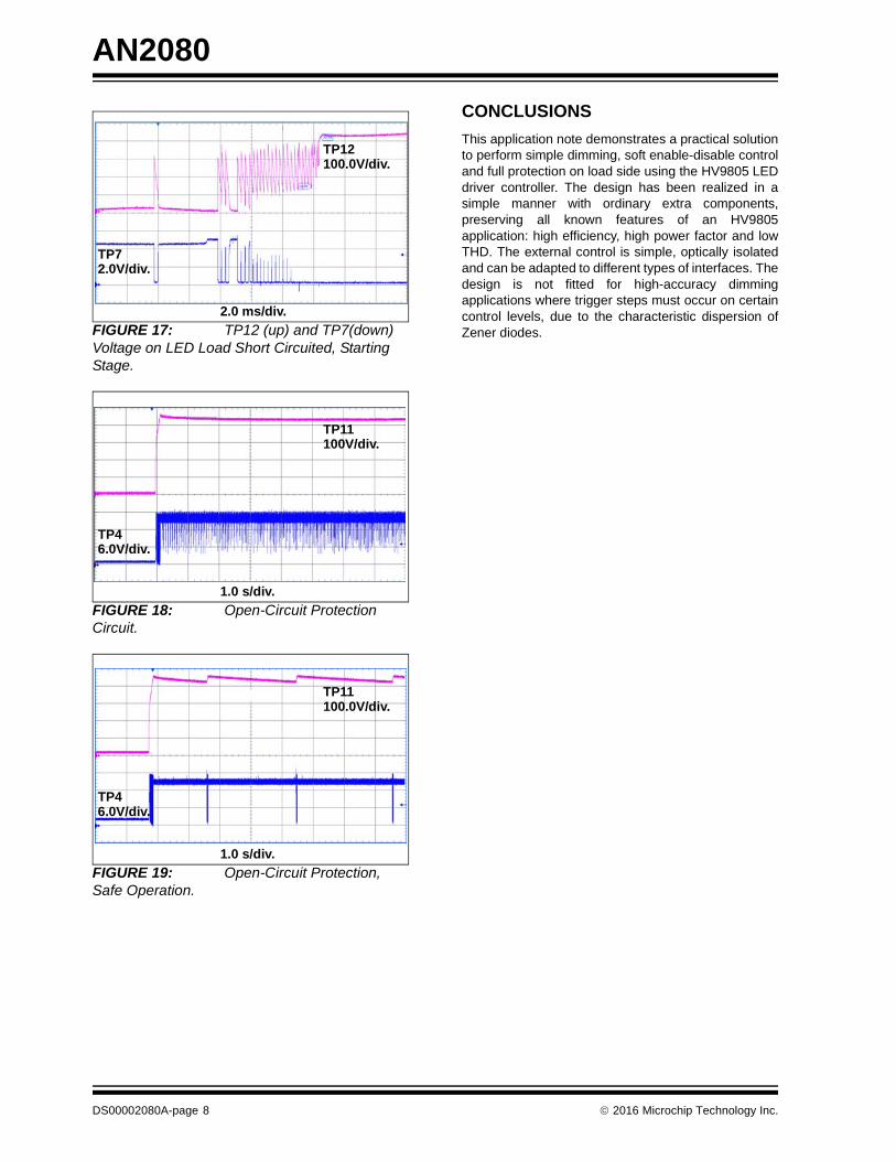
The working principle of the short-circuit protection(SCP) is that when TP11 and TP12 (see Figure 6 andthe schematic in Appendix A) are accidentallyconnected (producing LED load short circuit), M2 willbe turned OFF immediately and the controller will gointo an open-circuit condition. In that moment, the TP11voltage will be charged and discharged between thepreset Overvoltage Protection values (e.g. 410V and435V, see TP11 wave in Figure 19). Note that the shortperiod charging procedure is to provide energy to theHV9805 controller right after VDD hits the lowestthreshold. The M2 transistor must be rated for morethan 500V, which is above the OVP threshold. Thecurrent schematic uses a 650V rated MOSFET. AnRCD snubber network was added across M2 (R26,C13, D3, see Figure 6) to limit overshoot voltagesduring short-circuit conditions. The triggering voltage(VTRIG) of TP12 cannot be too low (not lower than 60V)for determining the SCP condition. Too low triggeringvoltage will make the system unable to startup or, whenpowering off, unable to immediately power up again.The triggering voltage can be roughly calculated asfollows:
EQUATION 1:
Setting the VTRIG to approximately 100V will ensureenough margin for the temperature change, as VBEvoltage decreases with increased temperature.
FIGURE 6: Short-Circuit Protection.
When M2 turns off:
VR23 0.6V
VD2 4.7V
VR13 5.3V
At room temperature:
IR135.3V
82 k--------------- 65 A= =
ID20.6V
3.9 k---------------- 154 A= =
Then:
VTRIG IR13 ID2+ R12 R12A R12B+ + VR13+=
~104V=
82kR13
13
4.7VD2
GND
12
J3
12
J4
TP11
TP12
150kR12A
150kR12
3k9R23
GND
13
2
MMBT2222A
Q1
GND 21
3
IPD65R250C6XTMA1CTM2
150kR12B
0RR24
330kR25
560 pFC14
2k2R26
220 pFC13
STTH1L06A
D3
6V8D4
GNDGNDGND
TP8
2016 Microchip Technology Inc. DS00002080A-page 5
AN2080
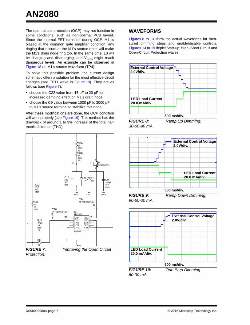
The open-circuit protection (OCP) may not function insome conditions, such as non-optimal PCB layout.Since the internal FET turns off during OCP, M1 isbiased at the common gate amplifier condition; anyringing that occurs at the M1's source node will makethe M1's drain node ring too. In the same time, L3 willbe charging and discharging, and VBUS might reachdangerous levels. An example can be observed inFigure 18 on M1's source waveform (TP4).
To solve this possible problem, the current designschematic offers a solution for the most effective circuitchanges (see TP11 wave in Figure 19). They are asfollows (see Figure 7):
• choose the C22 value from 15 pF to 20 pF for increased damping effect on M1's drain node.
• choose the C9 value between 1000 pF to 3000 pF to M1's source terminal to stabilize this node.
After these modifications are done, the OCP conditionwill work properly (see Figure 19). This method has thedrawback of around 1 to 3% increase of the total har-monic distortion (THD).
FIGURE 7: Improving the Open Circuit Protection.
WAVEFORMS
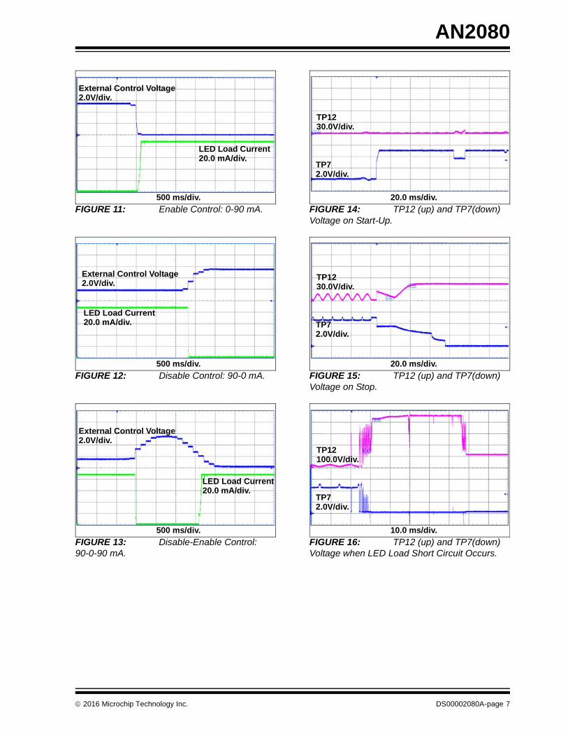
Figures 8 to 13 show the actual waveforms for mea-sured dimming steps and enable/disable controls.Figures 14 to 19 depict Start-up, Stop, Short Circuit andOpen-Circuit Protection waves.
This application note demonstrates a practical solutionto perform simple dimming, soft enable-disable controland full protection on load side using the HV9805 LEDdriver controller. The design has been realized in asimple manner with ordinary extra components,preserving all known features of an HV9805application: high efficiency, high power factor and lowTHD. The external control is simple, optically isolatedand can be adapted to different types of interfaces. Thedesign is not fitted for high-accuracy dimmingapplications where trigger steps must occur on certaincontrol levels, due to the characteristic dispersion ofZener diodes.
TP12
TP7
2.0 ms/div.
100.0V/div.
2.0V/div.
TP11
TP4
1.0 s/div.
100V/div.
6.0V/div.
TP11
TP4
1.0 s/div.
100.0V/div.
6.0V/div.
DS00002080A-page 8 2016 Microchip Technology Inc.
2
01
6 M
icroch
ip T
ech
no
log
y Inc.
DS
00
00
20
80
A-p
ag
e 9
AN
2080
AP
Figap
FIG
6M
L
33R12061%
R11A33R12061%
R11B
GND
82k08051%
R13
13
4.7VD2
D
TP PAD PCB 1.6x1TP8
12
MKDSN2,5/2-5.08
J3
12
MKDSN2,5/2-5.08
J4
TP 11
TP 12
33R12061%
R11C
GND GND
VDD
U2U3T
33R12061%
R17
150k08051%
R12A
150k08051%
R12
3k908051%
R23
GND
13
2
MMBT2222A
Q1
GND 21
3
IPD65R250C6XTMA1CTM2
150k08051%
R12B
0R08051%
R24
330k08051%
R25
GND
560 pF50V
0805
C14
GND
2k225125%
R26
220 pF1KV1206
C13
10k08051%
R910k08051%
R11
1A / 600VSTTH1L06A
D3
DG
S
M4
DMN6140L
DG
S
M3
DMN6140L
D
6V8D4
PENDIX A: BOARD SCHEMATIC
ure 20 shows the complete schematic of a 230VAC Three-Step Dimmingplication using the HV9805 device.
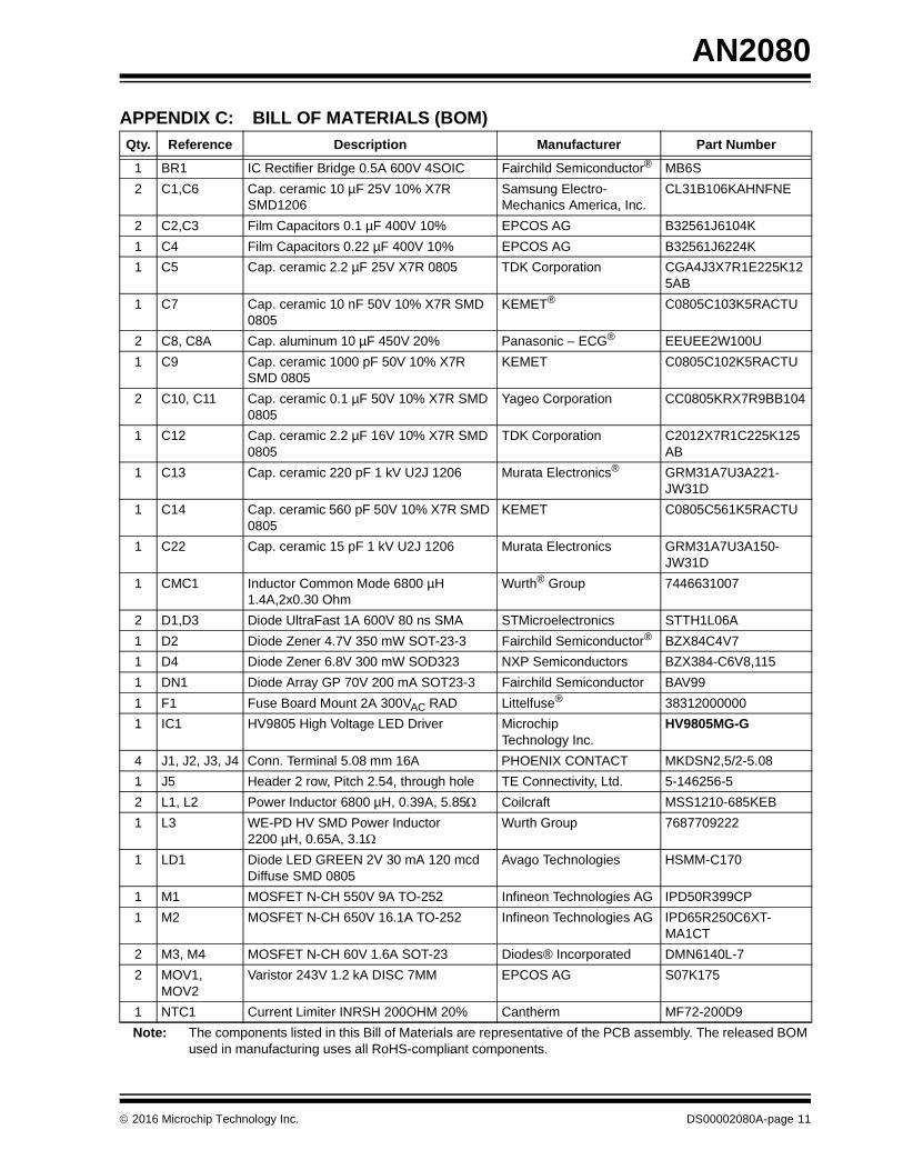
1 NTC1 Current Limiter INRSH 200OHM 20% Cantherm MF72-200D9
Note: The components listed in this Bill of Materials are representative of the PCB assembly. The released BOMused in manufacturing uses all RoHS-compliant components.
2016 Microchip Technology Inc. DS00002080A-page 11
2 Z3,Z5 Diode Zener 3.3V 1.5W SMA ON Semiconductor® 1SMA5913BT3G
1 Z4 Diode Zener 6.8V 1.5W SMA ON Semiconductor 1SMA5921BT3G
APPENDIX C: BILL OF MATERIALS (BOM) (CONTINUED)
Qty. Reference Description Manufacturer Part Number
Note: The components listed in this Bill of Materials are representative of the PCB assembly. The released BOMused in manufacturing uses all RoHS-compliant components.
DS00002080A-page 12 2016 Microchip Technology Inc.
AN2080
APPENDIX D: MEASURED INPUT - OUTPUT PARAMETERS
Input Current (mA)
Output Current (mA)
Input Power (W)
Output Power (W)
Efficiency (%) Power FactorATHD(%)
60 31 13 11.6 89 0.883 16.3
110 58 25 22.7 91 0.962 8.25
160 86 38 34.9 92 0.975 5.86
APPENDIX E: CONFIGURATION TABLE FOR ENABLE-DISABLE AND LED LOAD LIGHT LEVEL RELATED TO EXTERNAL CONTROL VOLTAGE
External Control Voltage
(V)
J5 - Jumper Position LED Load Light Level (%)
Disable1-2 3-4 5-6 100 66 33
0-10
<3.3
>3.3 ON
>6.7
Legend: blank = unpopulated/not active
= populated jumper (position short-circuited)
= either populated or unpopulated
= actual light level
2016 Microchip Technology Inc. DS00002080A-page 13
AN2080
NOTES:
DS00002080A-page 14 2016 Microchip Technology Inc.
Note the following details of the code protection feature on Microchip devices:
• Microchip products meet the specification contained in their particular Microchip Data Sheet.
• Microchip believes that its family of products is one of the most secure families of its kind on the market today, when used in the intended manner and under normal conditions.
• There are dishonest and possibly illegal methods used to breach the code protection feature. All of these methods, to our knowledge, require using the Microchip products in a manner outside the operating specifications contained in Microchip’s Data Sheets. Most likely, the person doing so is engaged in theft of intellectual property.
• Microchip is willing to work with the customer who is concerned about the integrity of their code.
• Neither Microchip nor any other semiconductor manufacturer can guarantee the security of their code. Code protection does not mean that we are guaranteeing the product as “unbreakable.”
Code protection is constantly evolving. We at Microchip are committed to continuously improving the code protection features of ourproducts. Attempts to break Microchip’s code protection feature may be a violation of the Digital Millennium Copyright Act. If such actsallow unauthorized access to your software or other copyrighted work, you may have a right to sue for relief under that Act.
Information contained in this publication regarding deviceapplications and the like is provided only for your convenienceand may be superseded by updates. It is your responsibility toensure that your application meets with your specifications.MICROCHIP MAKES NO REPRESENTATIONS ORWARRANTIES OF ANY KIND WHETHER EXPRESS ORIMPLIED, WRITTEN OR ORAL, STATUTORY OROTHERWISE, RELATED TO THE INFORMATION,INCLUDING BUT NOT LIMITED TO ITS CONDITION,QUALITY, PERFORMANCE, MERCHANTABILITY ORFITNESS FOR PURPOSE. Microchip disclaims all liabilityarising from this information and its use. Use of Microchipdevices in life support and/or safety applications is entirely atthe buyer’s risk, and the buyer agrees to defend, indemnify andhold harmless Microchip from any and all damages, claims,suits, or expenses resulting from such use. No licenses areconveyed, implicitly or otherwise, under any Microchipintellectual property rights unless otherwise stated.
2016 Microchip Technology Inc.
Microchip received ISO/TS-16949:2009 certification for its worldwide headquarters, design and wafer fabrication facilities in Chandler and Tempe, Arizona; Gresham, Oregon and design centers in California and India. The Company’s quality system processes and procedures are for its PIC® MCUs and dsPIC® DSCs, KEELOQ® code hopping devices, Serial EEPROMs, microperipherals, nonvolatile memory and analog products. In addition, Microchip’s quality system for the design and manufacture of development systems is ISO 9001:2000 certified.
QUALITY MANAGEMENT SYSTEM CERTIFIED BY DNV
== ISO/TS 16949 ==
Trademarks
The Microchip name and logo, the Microchip logo, AnyRate, dsPIC, FlashFlex, flexPWR, Heldo, JukeBlox, KeeLoq, KeeLoq logo, Kleer, LANCheck, LINK MD, MediaLB, MOST, MOST logo, MPLAB, OptoLyzer, PIC, PICSTART, PIC32 logo, RightTouch, SpyNIC, SST, SST Logo, SuperFlash and UNI/O are registered trademarks of Microchip Technology Incorporated in the U.S.A. and other countries.
ClockWorks, The Embedded Control Solutions Company, ETHERSYNCH, Hyper Speed Control, HyperLight Load, IntelliMOS, mTouch, Precision Edge, and QUIET-WIRE are registered trademarks of Microchip Technology Incorporated in the U.S.A.
Analog-for-the-Digital Age, Any Capacitor, AnyIn, AnyOut, BodyCom, chipKIT, chipKIT logo, CodeGuard, dsPICDEM, dsPICDEM.net, Dynamic Average Matching, DAM, ECAN, EtherGREEN, In-Circuit Serial Programming, ICSP, Inter-Chip Connectivity, JitterBlocker, KleerNet, KleerNet logo, MiWi, motorBench, MPASM, MPF, MPLAB Certified logo, MPLIB, MPLINK, MultiTRAK, NetDetach, Omniscient Code Generation, PICDEM, PICDEM.net, PICkit, PICtail, PureSilicon, RightTouch logo, REAL ICE, Ripple Blocker, Serial Quad I/O, SQI, SuperSwitcher, SuperSwitcher II, Total Endurance, TSHARC, USBCheck, VariSense, ViewSpan, WiperLock, Wireless DNA, and ZENA are trademarks of Microchip Technology Incorporated in the U.S.A. and other countries.
SQTP is a service mark of Microchip Technology Incorporated in the U.S.A.
Silicon Storage Technology is a registered trademark of Microchip Technology Inc. in other countries.
GestIC is a registered trademarks of Microchip Technology Germany II GmbH & Co. KG, a subsidiary of Microchip Technology Inc., in other countries.
All other trademarks mentioned herein are property of their respective companies.


![SAMA5D3 Layout Recommendations - Microchip Technologyww1.microchip.com/downloads/en/AppNotes/Atmel... · SAMA5D3 Layout Recommendations [APPLICATION NOTE] 3 Atmel-11284B-ATARM-SAMA5D3](https://static.documents.pub/doc/80x56/5ec95b888c0173649011ce25/sama5d3-layout-recommendations-microchip-sama5d3-layout-recommendations-application.jpg)

