2018 Microchip Technology Inc. DS00002790A-page 1 INTRODUCTION The USB-to-SPI bridging feature provides system designers who use Microchip hubs an expanded system control and a potential BOM reduction. The use of a separate USB-to-SPI device is no longer required, and a downstream USB port is not lost as a result of implementing the standalone USB-to-SPI device. This feature is available on Microchip hubs that contain an internal Hub Feature Controller (HFC) and a Serial Peripheral Interface (SPI) interface. These hubs include USB7002, USB7050, USB7051 USB7052, and USB7056. Commands may be sent from the USB Host to the internal HFC device in the Microchip hub to perform the following functions: • Get hub information • Reset the hub • Force boot from internal ROM • Enable SPI pass-through interface • Disable SPI pass-through interface • SPI pass-through read/write Sections This document includes the following topics: General Information on page 2 Part Number Information on page 4 MPLABCC DLL Implementation on page 4 Low-Level Implementation on page 5 References Consult the following documents for details on the specific parts referred to in this document: • USB7002 Data Sheet • USB7050 Data Sheet • USB7051 Data Sheet • USB7052 Data Sheet • USB7056 Data Sheet • SST26VF016B Data Sheet • Configuration of the USB7002 and USB705x Application Note AN2790 USB-to-SPI Bridging with Microchip USB7002 and USB705x Hubs Author: Shiva Balasubramanian Microchip Technology Inc.
Transcript
AN2790USB-to-SPI Bridging with Microchip USB7002 and
USB705x Hubs
INTRODUCTION
The USB-to-SPI bridging feature provides system designers who use Microchip hubs an expanded system control and a potential BOM reduction. The use of a separate USB-to-SPI device is no longer required, and a downstream USB port is not lost as a result of implementing the standalone USB-to-SPI device. This feature is available on Microchip hubs that contain an internal Hub Feature Controller (HFC) and a Serial Peripheral Interface (SPI) interface. These hubs include USB7002, USB7050, USB7051 USB7052, and USB7056.
Commands may be sent from the USB Host to the internal HFC device in the Microchip hub to perform the following functions:
• Get hub information
• Reset the hub
• Force boot from internal ROM
• Enable SPI pass-through interface
• Disable SPI pass-through interface
• SPI pass-through read/write
Sections
This document includes the following topics:
General Information on page 2
Part Number Information on page 4
MPLABCC DLL Implementation on page 4
Low-Level Implementation on page 5
References
Consult the following documents for details on the specific parts referred to in this document:
• USB7002 Data Sheet
• USB7050 Data Sheet
• USB7051 Data Sheet
• USB7052 Data Sheet
• USB7056 Data Sheet
• SST26VF016B Data Sheet
• Configuration of the USB7002 and USB705x Application Note
Author: Shiva BalasubramanianMicrochip Technology Inc.
2018 Microchip Technology Inc. DS00002790A-page 1
AN2790
GENERAL INFORMATION
The USB7002/USB705x series of USB hubs support native USB Type-C on the upstream side and a combination of native USB Type-C and standard USB 2.0 ports on the downstream side. On successful enumeration of the hub, the USB device tree on the host shows a USB2.0 hub instance, a USB3.0 hub instance, and a third device which is the HFC. Refer to Table 1 for details on the default HFC settings by part number.
TABLE 1: DEFAULT SETTINGS FOR HUB FEATURE CONTROLLER ENABLE
Part Number Part SummaryHub Controller Default Setting
USB3 PID USB2 PID
USB7002 4-Port USB3.1 Gen1 Hub Enabled on Port 6 0x7002 0x4002
USB7050 4-Port USB3.1 Gen1 Hub with power delivery on 3 ports
Enabled on Port 6 0x7050 0x4050
USB7051 4-Port USB3.1 Gen1 Hub with power delivery on 2 ports
Enabled on Port 6 0x7051 0x4051
USB7052 4-Port USB3.1 Gen1 Hub with power delivery on 1 port
Enabled on Port 6 0x7052 0x4052
USB7056 6-Port USB3.1 Gen1 Hub with power delivery on 1 port
Enabled on Port 8 0x7056 0x4056
The HFC is a USB device that enumerates on an extra internal non-removable USB2.0 port (Figure 1). For example, in a 4-port hub, the HFC is connected to Port 5. The base Product ID (PID) for the HFC is 0x7040. Based on the features enabled in an SKU, the last nibble of this PID may vary. The HFC is enabled by default in all the SKUs and can be dis-abled by setting bit 8 of the runtime flag register at address 0xBFD23408.
To use the bridging features of the hub, all bridging host commands must be addressed to the HFC which in turn will transmit the data to the appropriate serial interface lines.
The host can get information about the hub by issuing the GET_HUB_INFO command. In response, the hub sends a packet that contains information about the device revision, firmware version, and boot mode.
RESET THE HUB
The host can soft reset the hub externally by issuing the CMD_DEV_RESET command. This forces the hub firmware to start execution from 0x000000 and go through the boot sequence again.
FORCE BOOT FROM INTERNAL ROM
In situations where the hub is executing out of an external SPI ROM and the host wants to perform SPI pass-through transfers with the SPI ROM, this command sequence can be used to force the hub to boot and execute from the internal ROM.
ENABLE THE SPI PASS-THROUGH INTERFACE
To acquire the SPI interface, the host must send a CMD_SPI_ENTER_PASSTHRU SETUP packet before performing any SPI read/write commands. The SPI interface may operate at either 30 MHz or 60 MHz.
DISABLE THE SPI PASS-THROUGH INTERFACE
The SPI pass-through interface can be disabled after read/write operations by sending a CMD_SPI_EXIT_PASSTHRU SETUP packet.
SPI PASS-THROUGH READ/WRITE
The SPI pass-through interface allows single-/multi-byte write access and read access. In case of these operations, the SPI interface functions as a complete pass-through, which means any SPI data sent as a payload in the USB transfer gets transferred to the SPI lines directly. Therefore, the host must properly arrange data payloads in the appropriate SPI-compatible format and bit order, including the SPI slave device address. Up to 256 bytes can be written to an SPI peripheral using an SPI Write command sequence.
Data can also be read from an SPI peripheral using a combination of SPI read/write pass-through transfers. The host first needs to send a SETUP packet that informs the hub about the number of bytes to be read. Following this command, the hub stores the requested data bytes in an internal register at 0xBFD22310. The SPI Read command sequence can then be initiated by the host to retrieve the data. Up to 512 bytes of data can be read per SPI Read command sequence.
SPI Interface SETUP Requirements
SPI MASTER INTERFACE
The SPI interface always acts as an SPI master.
SELECTING SPI FREQUENCY
The SPI interface can operate at either 30 MHz or 60 MHz. The hub firmware configures the SPI interface to operate at 60 MHz by default. This can be changed by writing to bit 7 of the SPI_CTL register at address 0xBF802400, where:
• 0 = 30 MHz
• 1 = 60 MHz
SPI firmware images are designed to operate at specific speeds. Refer to the release notes of the SPI firmware image in use prior to making any modifications to the SPI interface speed.
2018 Microchip Technology Inc. DS00002790A-page 3
AN2790
SPI MODES OF OPERATION
Both SPI modes 0 and 3 are supported:
• Mode 0: Clock Polarity = 0, Clock Edge = 1
• Mode 3: Clock Polarity = 1, Clock Edge = 0
Dual Output Enable mode is also supported.
The default mode of operation is Mode 0 with the Dual Output Enable mode disabled. If the mode of operation is to be modified, a register write to the SPI_CTL (0xBF802400) register must be performed.
PART NUMBER INFORMATION
Part Summary
In USB7002/705x devices, SPI interface signals are associated with dedicated pins. See Table 2 for information on the pins.
TABLE 2: USB7002 AND USB705X SPI INTERFACE PIN NUMBERS
DeviceSPI_DI/SPI_D1
SPI_CE_NSPI_DO/SPI_D0
SPI_CLK SPI_D2 SPI_D3
USB7002 71 69 70 68 72 73
USB7050 71 69 70 68 72 73
USB7051 71 69 70 68 72 73
USB7052 71 69 70 68 72 73
USB7056 71 69 70 68 72 73
MPLABCC DLL IMPLEMENTATION
The simplest method for implementing the USB-to-SPI bridging functions is to use the publicly available MPLABCC DLL. MPLABCC is available for Windows® operating system. Visit the product page on microchip.com for any of the hubs listed in this document and to download the MPLABCC package. Using the libraries available in MPLABCC, the bridging features can be implemented in the C programming language.
The MPLABCC package contains the following:
• User’s guide: A detailed description of how to use the DLL API to call each function
• Release notes
• Library files:
- For Windows, a “.dll” and a “.lib” file
• Example code
Commands Included in SDK
• MchpUsbSpiSetConfig: This API enables or disables the SPI interface.
• MchpUsbSpiFlashWrite: This API performs write operation to the SPI Flash memory.
• MchpUsbSpiFlashRead: This API performs read operation from the SPI Flash memory.
• MchpUsbSpiTransfer: This API performs write operation to the SPI interface. SPI transfer to and from arbitrary SPI slaves is not supported.
For additional details on how to use the MPLABCC DLL for implementation of USB-to-SPI bridging, download the MPLABCC package and refer to the user’s guide.
DS00002790A-page 4 2018 Microchip Technology Inc.
AN2790
LOW-LEVEL IMPLEMENTATION
The USB-to-SPI bridging features may be implemented at the lowest level if you have the ability to build USB packets. This approach is required if Windows or the SDK cannot be used.
The details of these low-level USB packets are shown in the following sub-sections.
Get Hub Information
The following GET_HUB_INFO SETUP packet must be sent to obtain the hub-related information (Figure 2). Refer to Table 3 for the USB SETUP command details.
TABLE 3: USB SETUP COMMAND: GET HUB INFORMATION
SETUP Packet Value Description
bmRequestType 0xC0 Host-to-device data transfer with a vendor-specific command that targets the device
bRequest 0x09 GET_HUB_INFO command
wValue 0x0000 Reserved
wIndex 0x0000 Reserved
wLength 0x0006 Size of the HUB_INFO structure
The hub responds with a Hub Information Structure (HUB_INFO) during the DATA phase (Figure 2). The details on the hub information structure (DATA phase) are in Table 4.
TABLE 4: HUB INFORMATION STRUCTURE (DATA PHASE)
Offset Size Field Description
0x00 2 FW Revision Firmware revision
0x02 1 Device Revision Silicon mask revision
0x03 2 ASIC Type ASIC type:0xA00xB0
0x05 1 Feature Flag Bit 0: Current code execution area; 0: ROM, 1: SPI
FIGURE 2: GET_HUB_INFO (SETUP AND DATA PHASE)
Feature Flag
2018 Microchip Technology Inc. DS00002790A-page 5
AN2790
Reset the Hub
The hub can be soft reset externally from the host by issuing the CMD_DEV_RESET command. This command does not have a DATA phase (Figure 3). The existing device handle becomes invalid when the hub is reset. The host must acquire a new device handle by reopening the hub. See Table 5 for the USB SETUP command information.
TABLE 5: USB SETUP COMMAND: RESETTING THE HUB
SETUP Packet Value Description
bmRequestType 0x41 Host-to-device data transfer with a vendor-specific command that targets the device
bRequest 0x29 CMD_DEV_RESET command
wValue 0x0001 Reserved
wIndex 0x0000 Reserved
wLength 0x0000 No DATA phase
FIGURE 3: RESETTING THE HUB (SETUP PHASE)
Force Boot from Internal ROM
If the hub is executing out of the external SPI ROM and the host must perform SPI pass-through operations on the SPI ROM, then the hub must be forced to execute from the internal ROM for the operations to succeed. This can be achieved with the following command sequence:
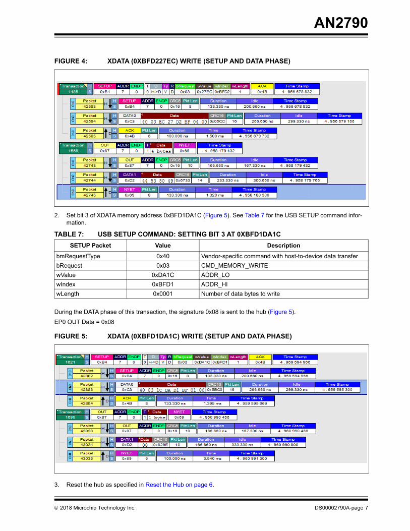
1. Write the disable the SPI (DSPI) signature to the XDATA memory location 0xBFD227EC (Figure 4). The hub checks for this signature during the boot sequence. Refer to Table 6 for the USB SETUP command.
TABLE 6: USB SETUP COMMAND: WRITING DSPI SIGNATURE
SETUP Packet Value Description
bmRequestType 0x40 Vendor-specific command with host-to-device data transfer
bRequest 0x03 CMD_MEMORY_WRITE
wValue 0x27EC ADDR_LO
wIndex 0xBFD2 ADDR_HI
wLength 0x0004 Number of data bytes to write
During the DATA phase of this transaction, the DSPI signature is sent to the hub.
EP0 OUT Data = 0x44, 0x53, 0x50, 0x49 (‘D’, ‘S’, 'P’, ‘I’)
DS00002790A-page 6 2018 Microchip Technology Inc.
AN2790
FIGURE 4: XDATA (0XBFD227EC) WRITE (SETUP AND DATA PHASE)
2. Set bit 3 of XDATA memory address 0xBFD1DA1C (Figure 5). See Table 7 for the USB SETUP command infor-mation.
TABLE 7: USB SETUP COMMAND: SETTING BIT 3 AT 0XBFD1DA1C
SETUP Packet Value Description
bmRequestType 0x40 Vendor-specific command with host-to-device data transfer
bRequest 0x03 CMD_MEMORY_WRITE
wValue 0xDA1C ADDR_LO
wIndex 0xBFD1 ADDR_HI
wLength 0x0001 Number of data bytes to write
During the DATA phase of this transaction, the signature 0x08 is sent to the hub (Figure 5).
EP0 OUT Data = 0x08
FIGURE 5: XDATA (0XBFD1DA1C) WRITE (SETUP AND DATA PHASE)
3. Reset the hub as specified in Reset the Hub on page 6.
2018 Microchip Technology Inc. DS00002790A-page 7
AN2790
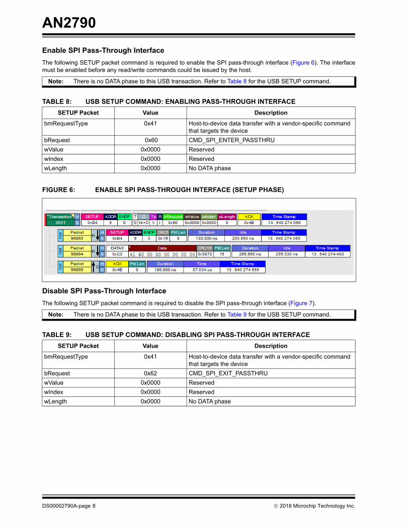
Enable SPI Pass-Through Interface
The following SETUP packet command is required to enable the SPI pass-through interface (Figure 6). The interface must be enabled before any read/write commands could be issued by the host.
TABLE 8: USB SETUP COMMAND: ENABLING PASS-THROUGH INTERFACE
SETUP Packet Value Description
bmRequestType 0x41 Host-to-device data transfer with a vendor-specific command that targets the device
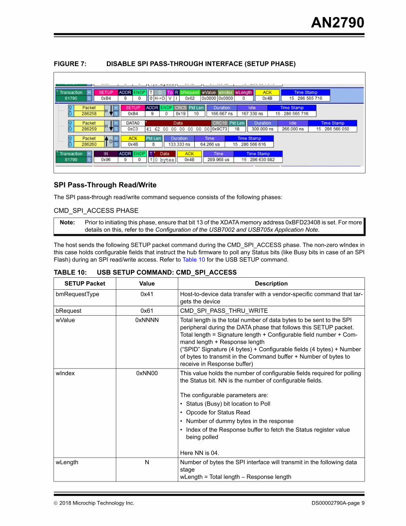
The SPI pass-through read/write command sequence consists of the following phases:
CMD_SPI_ACCESS PHASE
Note: Prior to initiating this phase, ensure that bit 13 of the XDATA memory address 0xBFD23408 is set. For more details on this, refer to the Configuration of the USB7002 and USB705x Application Note.
The host sends the following SETUP packet command during the CMD_SPI_ACCESS phase. The non-zero wIndex in this case holds configurable fields that instruct the hub firmware to poll any Status bits (like Busy bits in case of an SPI Flash) during an SPI read/write access. Refer to Table 10 for the USB SETUP command.
TABLE 10: USB SETUP COMMAND: CMD_SPI_ACCESS
SETUP Packet Value Description
bmRequestType 0x41 Host-to-device data transfer with a vendor-specific command that tar-gets the device
bRequest 0x61 CMD_SPI_PASS_THRU_WRITE
wValue 0xNNNN Total length is the total number of data bytes to be sent to the SPI peripheral during the DATA phase that follows this SETUP packet.Total length = Signature length + Configurable field number + Com-mand length + Response length(“SPID” Signature (4 bytes) + Configurable fields (4 bytes) + Number of bytes to transmit in the Command buffer + Number of bytes to receive in Response buffer)
wIndex 0xNN00 This value holds the number of configurable fields required for polling the Status bit. NN is the number of configurable fields.
The configurable parameters are:
• Status (Busy) bit location to Poll
• Opcode for Status Read
• Number of dummy bytes in the response
• Index of the Response buffer to fetch the Status register value being polled
Here NN is 04.
wLength N Number of bytes the SPI interface will transmit in the following data stagewLength = Total length – Response length
2018 Microchip Technology Inc. DS00002790A-page 9
AN2790
DATA PHASE
During this phase, the host sends an OUT DATA packet to the SPI peripheral. This packet is formatted as follows:
EP0 DATA =
• Index 0: S (0x53)
• Index 1: P (0x50)
• Index 2: I (0x49)
• Index 3: D (0x44)
• Index 4: Busy bit (0x01)
• Index 5: Read Status opcode
• Index 6: Number of dummy bytes in response
• Index 7: Index of the Response buffer to fetch the Status register value being polled
• Index 8 to Index n: Command buffer data (command byte, address byte, dummy bytes, and up to 256 data bytes)
RETRIEVING THE DATA (APPLIES TO BLOCK READ ONLY)
These additional SETUP and DATA phases are applicable only in case of SPI Block Reads. During the previous DATA phase (see Data Phase on page 10), based on the opcode, the hub retrieves the requested number of data bytes from the SPI peripheral and stores it internally in a register at location 0xBFD22310.
During this phase, the hub first sends the following SETUP packet to read the hub’s internal register that contains the requested data. See Table 11 for the USB SETUP command.
TABLE 11: USB SETUP COMMAND: SPI BLOCK READ
SETUP Packet Value Description
bmRequestType 0xC0 Vendor-specific command with device-to-host to data transfer
bRequest 0x04 CMD_MEMORY_READ
wValue 0x2310 ADDR_LO
wIndex 0xBFD2 ADDR_HI
wLength 0xNNNN Number of data bytes to be retrieved
This is followed by a DATA phase where the hub responds to the host with an IN packet containing the requested number of bytes retrieved from the SPI peripheral.
DS00002790A-page 10 2018 Microchip Technology Inc.
AN2790
Single-Byte Instruction Write Example
Figure 8 shows an example where a single-byte instruction (WREN) is written to enable the write latch in case of a SST26VF016B SPI Flash memory. Refer to Table 12 for the USB SETUP command information.
TABLE 12: USB SETUP COMMAND: SPI SINGLE-BYTE WRITE
SETUP Packet Value Description
bmRequestType 0x41 Host-to-device data transfer with a vendor-specific command that targets the device
bRequest 0x61 CMD_SPI_PASS_THRU_WRITE
wValue 0x0009 Total length = Signature length (4 bytes) + Configurable field number (4 bytes) + Command length (1 byte) + Response length (0 byte)
wIndex 0x0400 Number of configurable fields for polling status
The configurable parameters are:
• Busy bit location to Poll (0x01)
• RDSR opcode (0x05)
• Number of dummy bytes in the response (0x00)
• Index of the Response buffer to fetch the Status register value that was returned (0x01)
wLength 0x0009 Number of bytes the SPI interface will transmit in the following data stage.wLength = Total length – Response lengthwLength = 9 – 0 = 9 bytes
0x05 is the Read Status register (RDSR) instruction, and 0xC7 is the Chip Erase instruction for SST26VF016B.
During the DATA phase of this command sequence, the host sends an OUT packet containing nine bytes to the SPI Flash as shown in Figure 8.
EP0 OUT Data =
• Index 0: S (0x53)
• Index 1: P (0x50)
• Index 2: I (0x49)
• Index 3: D (0x44)
• Index 4: Busy Bit (0x01)
• Index 5: Read Status opcode (RDSR:0x05)
• Index 6: Number of dummy bytes in response (0x00)
• Index 7: Index of the Response buffer to fetch the read status byte (0x01)
• Index 8 to Index 9: Command buffer data [Command byte: Chip Erase (0xC7)]
2018 Microchip Technology Inc. DS00002790A-page 11
AN2790
FIGURE 8: SINGLE-BYTE SPI WRITE (SETUP AND DATA PHASE)
Chip Erase
RDSR
SPI Block Write Example
The SPI pass-through interface allows the host to perform a block write of up to 256 bytes. Figure 9 shows the SETUP packet for performing a block write to a SST26VF016B SPI Flash memory. See Table 13 for the USB SETUP command details.
TABLE 13: USB SETUP COMMAND: SPI BLOCK WRITE
SETUP Packet Value Description
bmRequestType 0x41 Host-to-device data transfer with a vendor-specific command that targets the device
bRequest 0x61 CMD_SPI_PASS_THRU_WRITE
wValue 0x010C Total length = Signature length (4 bytes) + Configurable field number (4 bytes) + Command length (1-byte opcode + 3 bytes of address + 256 data bytes) + Response length (0 byte)
wIndex 0x0400 Number of configurable fields for polling status.
The configurable parameters are:
• Busy bit location to Poll (0x01)
• RDSR opcode (0x05)
• Number of dummy bytes in the response (0x00)
• Index of the Response buffer to fetch the Status register value that was returned (0x01)
wLength 0x010C Number of bytes the SPI interface will transmit in the following data stagewLength = Total length – Response lengthwLength = 268 – 0 = 268 bytes (0x010C)
DS00002790A-page 12 2018 Microchip Technology Inc.
AN2790
FIGURE 9: SPI BLOCK WRITE (SETUP PHASE)
During the DATA phase (Figure 10) of this command sequence, 268 bytes are transferred to the SPI Flash via the hub’s pass-through interface. The DATA packet consists of the following:
EP0 OUT Data =
• Index 0: S (0x53)
• Index 1: P (0x50)
• Index 2: I (0x49)
• Index 3: D (0x44)
• Index 4: Busy bit (0x01)
• Index 5: Read Status opcode (RDSR:0x05)
• Index 6: Number of dummy bytes in response (0x00)
• Index 7: Index of the Response buffer to fetch the read status byte (0x01)
• Index 8 to Index 267: Command buffer data [Command byte: PAGE PROGRAM (0x02), address byte (0x00, 0x00, 0x00), dummy byte (none), and up to 256 data bytes]
In this case, PAGE PROGRAM (0x02) instruction is specific to SST26VF016B.
FIGURE 10: SPI BLOCK WRITE (DATA PHASE)
Page Program
2018 Microchip Technology Inc. DS00002790A-page 13
AN2790
SPI Block Read Example
The SPI pass-through interface allows the host to perform a block read of up to 512 bytes. Figure 11 shows the SETUP packet for this transaction in case of a SST26VF016B SPI Flash memory. See Table 14 for the USB SETUP command information.
TABLE 14: USB SETUP COMMAND: SPI BLOCK READ
SETUP Packet Value Description
bmRequestType 0x41 Host-to-device data transfer with a vendor-specific command that targets the device
bRequest 0x61 CMD_SPI_PASS_THRU_WRITE
wValue 0x0212 Total length = Signature length (4 bytes) + Configurable field number (4 bytes) + Command length (1-byte opcode + 3 bytes of address +1 dummy byte) + Response length (512 data bytes) + 5 bytes (first five bytes to be ignored)
wIndex 0x0400 Number of configurable fields for polling status.
The configurable parameters are:
• Busy bit location to Poll (0x01)
• RDSR opcode (0x05)
• Number of dummy bytes in the response (0x00)
• Index of the Response buffer to fetch the Status register value that was returned (0x01)
wLength 0x000D Number of bytes the SPI interface will transmit in the following data stagewLength = Total length – Response lengthwLength = 530 – 517 = 13 bytes (0x000D)
FIGURE 11: SPI BLOCK READ (SETUP PHASE 1 AND DATA PHASE 1)
High Speed Read
During the DATA phase (Figure 11), 13 bytes are transferred to the hub. The DATA packet consists of the following:
EP0 OUT Data =
• Index 0: S (0x53)
• Index 1: P (0x50)
• Index 2: I (0x49)
DS00002790A-page 14 2018 Microchip Technology Inc.
AN2790
• Index 3: D (0x44)
• Index 4: Busy bit (0x01)
• Index 5: Read Status opcode (RDSR:0x05)
• Index 6: Number of dummy bytes in response (0x00)
• Index 7: Index of the Response buffer to fetch the read status byte (0x01)
• Index 8 to Index 12: Command buffer data [Command byte: HIGH SPEED READ (0x0B), address byte (0x02, 0x82, 0x00), dummy byte (0x00)]
In this case, HIGH-SPEED READ (0x0B) instruction is specific to SST26VF016B.
The host then initiates the second SETUP phase by sending a SETUP packet for reading the hub’s internal register at 0xBFD22310 containing the data bytes to be read. Figure 12 shows this SETUP packet. Refer to Table 15 for the USB SETUP command details.
TABLE 15: USB SETUP COMMAND: SPI BLOCK READ
SETUP Packet Value Description
bmRequestType 0xC0 Vendor-specific command with device-to-host-to-data transfer
bRequest 0x04 CMD_MEMORY_READ
wValue 0x2310 ADDR_LO
wIndex 0xBFD2 ADDR_HI
wLength 0x0205 Number of data bytes to be retrieved (517 bytes). The first five bytes of any SPI read must be ignored. There-fore, five must be added to the number of bytes to be read.
FIGURE 12: SPI BLOCK READ (SETUP PHASE 2 AND DATA PHASE 2)
First 5 bytes to be ignored
During the DATA phase that follows this, the hub responds with IN packets (Figure 12) containing a total of 517 bytes retrieved from the SPI Flash via the pass-through interface. The first five bytes returned during the DATA phase are 0s, and they need to be ignored.
2018 Microchip Technology Inc. DS00002790A-page 15
AN2790
APPENDIX A: APPLICATION NOTE REVISION HISTORY
TABLE A-1: REVISION HISTORY
Revision Level & Date Section/Figure/Entry Correction
DS00002790A(09-12-18)
Initial release
DS00002790A-page 16 2018 Microchip Technology Inc.
AN2790
NOTES:
2018 Microchip Technology Inc. DS00002790A-page 17
AN2790
DS00002790A-page 18 2018 Microchip Technology Inc.
THE MICROCHIP WEB SITE
Microchip provides Online support via our WWW site at www.microchip.com. This web site is used as a means to make files and information easily available to customers. Accessible by using your favorite Internet browser, the web site contains the following information:
• Product Support – Data sheets and errata, application notes and sample programs, design resources, user’s guides and hardware support documents, latest software releases and archived software
• General Technical Support – Frequently Asked Questions (FAQ), technical support requests, online discussion groups, Microchip consultant program member listing
• Business of Microchip – Product selector and ordering guides, latest Microchip press releases, listing of seminars and events, listings of Microchip sales offices, distributors and factory representatives
CUSTOMER CHANGE NOTIFICATION SERVICE
Microchip’s customer notification service helps keep customers current on Microchip products. Subscribers will receive e-mail notification whenever there are changes, updates, revisions or errata related to a specified product family or development tool of interest.
To register, access the Microchip web site at www.microchip.com. Under “Support”, click on “Customer Change Notifi-cation” and follow the registration instructions.
CUSTOMER SUPPORT
Users of Microchip products can receive assistance through several channels:
• Distributor or Representative
• Local Sales Office
• Field Application Engineer (FAE)
• Technical Support
Customers should contact their distributor, representative or Field Application Engineer (FAE) for support. Local sales offices are also available to help customers. A listing of sales offices and locations is included in the back of this document.
Technical support is available through the web site at: http://microchip.com/support
2018 Microchip Technology Inc. DS00002790A-page 19
Note the following details of the code protection feature on Microchip devices:
• Microchip products meet the specification contained in their particular Microchip Data Sheet.
• Microchip believes that its family of products is one of the most secure families of its kind on the market today, when used in the intended manner and under normal conditions.
• There are dishonest and possibly illegal methods used to breach the code protection feature. All of these methods, to our knowledge, require using the Microchip products in a manner outside the operating specifications contained in Microchip’s Data Sheets. Most likely, the person doing so is engaged in theft of intellectual property.
• Microchip is willing to work with the customer who is concerned about the integrity of their code.
• Neither Microchip nor any other semiconductor manufacturer can guarantee the security of their code. Code protection does not mean that we are guaranteeing the product as “unbreakable.”
Code protection is constantly evolving. We at Microchip are committed to continuously improving the code protection features of our products. Attempts to break Microchip’s code protection feature may be a violation of the Digital Millennium Copyright Act. If such acts allow unauthorized access to your software or other copyrighted work, you may have a right to sue for relief under that Act.
Microchip received ISO/TS-16949:2009 certification for its worldwide headquarters, design and wafer fabrication facilities in Chandler and Tempe, Arizona; Gresham, Oregon and design centers in California and India. The Company’s quality system processes and procedures are for its PIC® MCUs and dsPIC® DSCs, KEELOQ® code hopping devices, Serial EEPROMs, microperipherals, nonvolatile memory and analog products. In addition, Microchip’s quality system for the design and manufacture of development systems is ISO 9001:2000 certified.
QUALITYMANAGEMENTSYSTEMCERTIFIEDBYDNV
== ISO/TS16949==
Information contained in this publication regarding device applications and the like is provided only for your convenience and may be superseded by updates. It is your responsibility to ensure that your application meets with your specifications. MICROCHIP MAKES NO REPRESENTATIONS OR WARRANTIES OF ANY KIND WHETHER EXPRESS OR IMPLIED, WRITTEN OR ORAL, STATUTORY OR OTHERWISE, RELATED TO THE INFORMATION, INCLUDING BUT NOT LIMITED TO ITS CONDITION, QUALITY, PERFORMANCE, MERCHANTABILITY OR FITNESS FOR PURPOSE. Microchip disclaims all liability arising from this information and its use. Use of Micro-chip devices in life support and/or safety applications is entirely at the buyer’s risk, and the buyer agrees to defend, indemnify and hold harmless Microchip from any and all damages, claims, suits, or expenses resulting from such use. No licenses are conveyed, implicitly or otherwise, under any Microchip intellectual property rights unless otherwise stated.
Trademarks
The Microchip name and logo, the Microchip logo, AnyRate, AVR, AVR logo, AVR Freaks, BitCloud, chipKIT, chipKIT logo, CryptoMemory, CryptoRF, dsPIC, FlashFlex, flexPWR, Heldo, JukeBlox, KeeLoq, Kleer, LANCheck, LINK MD, maXStylus, maXTouch, MediaLB, megaAVR, MOST, MOST logo, MPLAB, OptoLyzer, PIC, picoPower, PICSTART, PIC32 logo, Prochip Designer, QTouch, SAM-BA, SpyNIC, SST, SST Logo, SuperFlash, tinyAVR, UNI/O, and XMEGA are registered trademarks of Microchip Technology Incorporated in the U.S.A. and other countries.
ClockWorks, The Embedded Control Solutions Company, EtherSynch, Hyper Speed Control, HyperLight Load, IntelliMOS, mTouch, Precision Edge, and Quiet-Wire are registered trademarks of Microchip Technology Incorporated in the U.S.A.
Adjacent Key Suppression, AKS, Analog-for-the-Digital Age, Any Capacitor, AnyIn, AnyOut, BodyCom, CodeGuard, CryptoAuthentication, CryptoAutomotive, CryptoCompanion, CryptoController, dsPICDEM, dsPICDEM.net, Dynamic Average Matching, DAM, ECAN, EtherGREEN, In-Circuit Serial Programming, ICSP, INICnet, Inter-Chip Connectivity, JitterBlocker, KleerNet, KleerNet logo, memBrain, Mindi, MiWi, motorBench, MPASM, MPF, MPLAB Certified logo, MPLIB, MPLINK, MultiTRAK, NetDetach, Omniscient Code Generation, PICDEM, PICDEM.net, PICkit, PICtail, PowerSmart, PureSilicon, QMatrix, REAL ICE, Ripple Blocker, SAM-ICE, Serial Quad I/O, SMART-I.S., SQI, SuperSwitcher, SuperSwitcher II, Total Endurance, TSHARC, USBCheck, VariSense, ViewSpan, WiperLock, Wireless DNA, and ZENA are trademarks of Microchip Technology Incorporated in the U.S.A. and other countries.
SQTP is a service mark of Microchip Technology Incorporated in the U.S.A.
Silicon Storage Technology is a registered trademark of Microchip Technology Inc. in other countries.
GestIC is a registered trademark of Microchip Technology Germany II GmbH & Co. KG, a subsidiary of Microchip Technology Inc., in other countries.
All other trademarks mentioned herein are property of their respective companies.