The information given in this document shall in no event be regarded as a guarantee of conditions or characteristics. With respect to any examples or hints given herein, any typical values stated herein and/or any information regarding the application of the device, Infineon Technologies hereby disclaims any and all warranties and liabilities of any kind, including without limitation, warranties of non-infringement of intellectual property rights of any third party.
Information
For further information on technology, delivery terms and conditions and prices, please contact the nearest Infineon Technologies Office (www.infineon.com).
Warnings
Due to technical requirements, components may contain dangerous substances. For information on the types in question, please contact the nearest Infineon Technologies Office.
Infineon Technologies components may be used in life-support devices or systems only with the express written approval of Infineon Technologies, if a failure of such components can reasonably be expected to cause the failure of that life-support device or system or to affect the safety or effectiveness of that device or system. Life support devices or systems are intended to be implanted in the human body or to support and/or maintain and sustain and/or protect human life. If they fail, it is reasonable to assume that the health of the user or other persons may be endangered.
Advanced Design System™ (ADS) of Agilent Technologies, AMBA™, ARM™, MULTI-ICE™, KEIL™, PRIMECELL™, REALVIEW™, THUMB™, µVision™ of ARM Limited, UK. AUTOSAR™ is licensed by AUTOSAR development partnership. Bluetooth™ of Bluetooth SIG Inc. CAT-iq™ of DECT Forum. COLOSSUS™, FirstGPS™ of Trimble Navigation Ltd. EMV™ of EMVCo, LLC (Visa Holdings Inc.). EPCOS™ of Epcos AG. FLEXGO™ of Microsoft Corporation. FlexRay™ is licensed by FlexRay Consortium. HYPERTERMINAL™ of Hilgraeve Incorporated. IEC™ of Commission Electrotechnique Internationale. IrDA™ of Infrared Data Association Corporation. ISO™ of INTERNATIONAL ORGANIZATION FOR STANDARDIZATION. MATLAB™ of MathWorks, Inc. MAXIM™ of Maxim Integrated Products, Inc. MICROTEC™, NUCLEUS™ of Mentor Graphics Corporation. MIPI™ of MIPI Alliance, Inc. MIPS™ of MIPS Technologies, Inc., USA. muRata™ of MURATA MANUFACTURING CO., MICROWAVE OFFICE™ (MWO) of Applied Wave Research Inc., OmniVision™ of OmniVision Technologies, Inc. Openwave™ Openwave Systems Inc. RED HAT™ Red Hat, Inc. RFMD™ RF Micro Devices, Inc. SIRIUS™ of Sirius Satellite Radio Inc. SOLARIS™ of Sun Microsystems, Inc. SPANSION™ of Spansion LLC Ltd. Symbian™ of Symbian Software Limited. TAIYO YUDEN™ of Taiyo Yuden Co. TEAKLITE™ of CEVA, Inc. TEKTRONIX™ of Tektronix Inc. TOKO™ of TOKO KABUSHIKI KAISHA TA. UNIX™ of X/Open Company Limited. VERILOG™, PALLADIUM™ of Cadence Design Systems, Inc. VLYNQ™ of Texas Instruments Incorporated. VXWORKS™, WIND RIVER™ of WIND RIVER SYSTEMS, INC. ZETEX™ of Diodes Zetex Limited.
1.1 Basics of Transient Voltage Suppression (TVS) Diodes
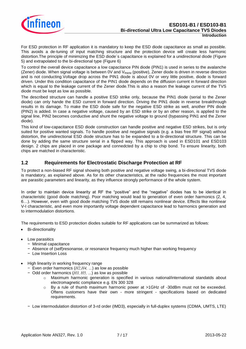
ESD protection devices are strongly nonlinear. Their characteristic is split into a working area, where devices act as “open” or “isolator”, and a protection area, where devices act as a “short” or “conductor”. Basic characteristic of a uni-directional ESD protection device including snap-back is shown in Figure 3 with some abbreviations in common use.
Physical principle of silicon based TVS diodes is the Zener or avalanche process wich drives the diode from an open into a short state, when operating voltage exceeds diode breakdown / trigger voltage VTrig. Silicon based TVS diodes offer following advantages over other approaches (MOV, MLV, polymer-based devices):
Both uni-directional (Figure 1) and bi-directional (Figure 2)structures are available
Rdyn can be kept very low even at low device capacitance
Low trigger voltage, low “first overshoot” lasting only about 1ns
Performance stable device, no degradation in leakage current performance even after multiple ESD strikes
Best ESD protection performance for high speed applications in the GHz range as well as for low frequency applications
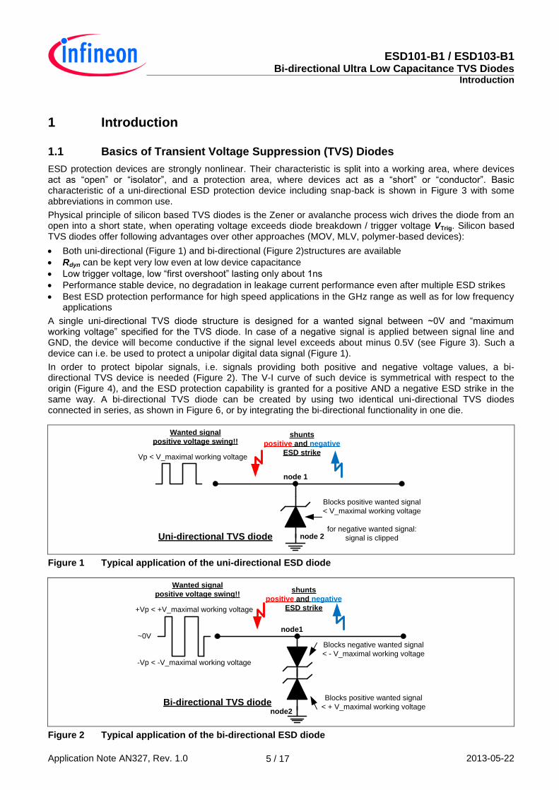
A single uni-directional TVS diode structure is designed for a wanted signal between ~0V and “maximum working voltage” specified for the TVS diode. In case of a negative signal is applied between signal line and GND, the device will become conductive if the signal level exceeds about minus 0.5V (see Figure 3). Such a device can i.e. be used to protect a unipolar digital data signal (Figure 1).
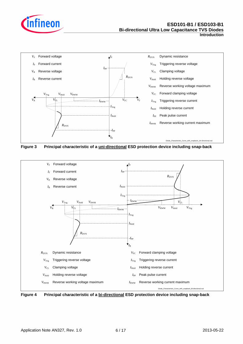
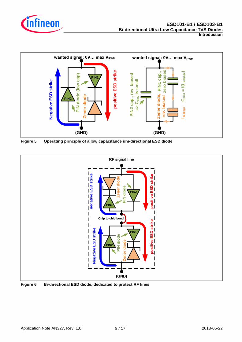
In order to protect bipolar signals, i.e. signals providing both positive and negative voltage values, a bi-directional TVS device is needed (Figure 2). The V-I curve of such device is symmetrical with respect to the origin (Figure 4), and the ESD protection capability is granted for a positive AND a negative ESD strike in the same way. A bi-directional TVS diode can be created by using two identical uni-directional TVS diodes connected in series, as shown in Figure 6, or by integrating the bi-directional functionality in one die.
Vp < V_maximal working voltage
Wanted signal
positive voltage swing!!shunts
positive and negative
ESD strike
Blocks positive wanted signal
< V_maximal working voltage
for negative wanted signal:
signal is clipped Uni-directional TVS diode
node 1
node 2
Figure 1 Typical application of the uni-directional ESD diode
+Vp < +V_maximal working voltage
~0V
Wanted signal
positive voltage swing!!
-Vp < -V_maximal working voltage
shunts
positive and negative
ESD strike
Blocks positive wanted signal
< + V_maximal working voltage
Blocks negative wanted signal
< - V_maximal working voltage
Bi-directional TVS diode
node1
node2
Figure 2 Typical application of the bi-directional ESD diode
For ESD protection in RF application it is mandatory to keep the ESD diode capacitance as small as possible. This avoids a de-tuning of input matching structure and the protection device will create less harmonic distortion.The principle of minimizing the ESD diode´s capacitance is explained for a unidirectional diode (Figure 5) and extrapolated to the bi-directional type (Figure 6)
To control the overall device capacitance a low capacitance PIN diode (PIN1) is used in series to the avalanche (Zener) diode. When signal voltage is between 0V and VRWM (positive), Zener diode is driven in reverse direction and is not conducting.Voltage drop across the PIN1 diode is about 0V or very little positive, diode is forward driven. Under this condition capacitance of the PIN1 diode depends on the diffusion current in forward direction which is equal to the leakage current of the Zener diode.This is also a reason the leakage current of the TVS diode must be kept as low as possible.
The described structure can handle a positive ESD strike only, because the PIN1 diode (serial to the Zener diode) can only hande the ESD current in forward direction. Driving the PIN1 diode in reverse breakthrough results in its damage. To make the ESD diode safe for the negative ESD strike as well, another PIN diode (PIN2) is added. In case a negative voltage, caused by an ESD strike or by an other reason, is applied to the signal line, PIN2 becomes conductive and shunt the negative voltage to ground (bypassing PIN1 and the Zener diode).
This kind of low-capacitance ESD diode construction can handle positive and negative ESD strikes, but is only suited for positive wanted signals. To handle positive and negative signals (e.g. a bias free RF signal) without distortion, the unidirectional ESD diode structure has to be expanded to a bi-directional structure. This can be done by adding the same structure serial in a flipped way. This approach is used in ESD101 and ESD103 design. 2 chips are placed in one package and connedcted by a chip to chip bond. To ensure linearity, both chips are matched in characteristic.
1.2 Requirements for Electrostatic Discharge Protection at RF
To protect a non-biased RF signal showing both positive and negative voltage swing, a bi-directional TVS diode is mandatory, as explained above. As for its other characteristics, at the radio frequencies the most important are parasitic parameters and linearity, as they influence strongly performance of the whole system.
In order to maintain device linearity at RF the “positive” and the “negative” diodes has to be identical in characteristic (good diode matching). Poor matching would lead to generation of even order harmonics (2, 4, 6…). However, even with good diode matching TVS diode still remains nonlinear device. Effects like nonlinear V-I characteristic, and even more importantly voltage dependent capacitance lead to harmonics generation and to intermodulation distortions.
The requirements to ESD protection diodes suitable for RF applications can be summarized as follows:
Bi-directionality
Low parasitics − Minimal capacitance − Absence of (self)resonanse, or resonance frequency much higher than working frequency − Low Insertion Loss
High linearity in working frequency range − Even order harmonics (H2,H4, …) as low as possible − Odd order harmonics (H3, H5, …) as low as possible
o Maximum harmonic generation is specified in various national/international standatds about electromagnetic compliance e.g. EN 300 328
o By a rule of thumb maximum harmonic power at >1GHz of -30dBm must not be exceeded. Oftens customers have their own - more stringent - specifications based on dedicated requirements.
− Low intermodulation distortion of 3-rd order (IMD3), especially in full-duplex systems (CDMA, UMTS, LTE)
Maximum working voltage VRWM = ±5.5 V VRWM = ±15 V
ESD protection of RF signal lines according to IEC61000-4-2 ±12 kV (contact), ±14 kV (air)
±10 kV (contact)
Extremely low capacitance CL = 0.1 pF (typical)1)
CL = 0.09 pF (typical) 1)
Very low reverse current IR < 0.1 nA IR < 0.1 nA
Extremely small form factor down to 0.62 x 0.32 x 0.31 mm² Yes Yes
Pb-free package (RoHS compliant)
1) at f = 1 GHz
2.2 Key Applications of ESD101-B1 / ESD103-B1
WLAN, GPS antenna, DVB T/H, Bluetooth Class 1 and 2
RF antenna
Super high speed interfaces
Connectivity applications
Automated Meter Reading
2.3 Description
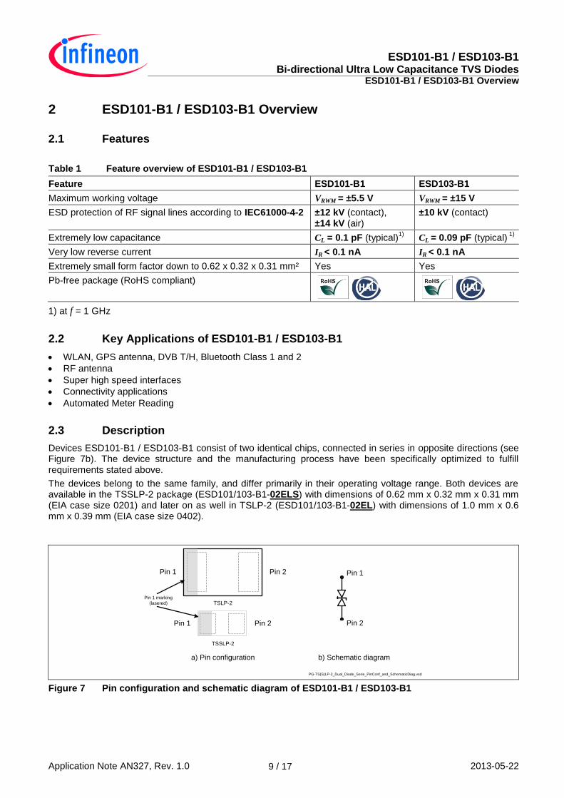
Devices ESD101-B1 / ESD103-B1 consist of two identical chips, connected in series in opposite directions (see Figure 7b). The device structure and the manufacturing process have been specifically optimized to fulfill requirements stated above.
The devices belong to the same family, and differ primarily in their operating voltage range. Both devices are available in the TSSLP-2 package (ESD101/103-B1-02ELS) with dimensions of 0.62 mm x 0.32 mm x 0.31 mm (EIA case size 0201) and later on as well in TSLP-2 (ESD101/103-B1-02EL) with dimensions of 1.0 mm x 0.6 mm x 0.39 mm (EIA case size 0402).
Figure 7 Pin configuration and schematic diagram of ESD101-B1 / ESD103-B1
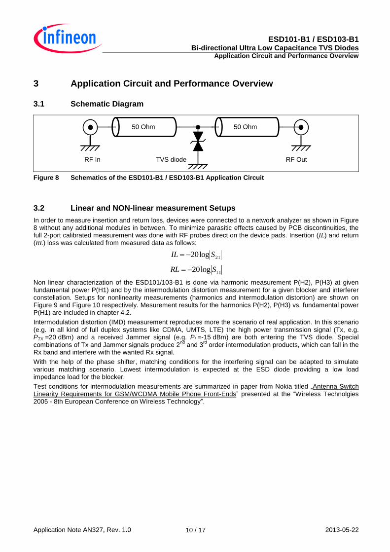
Figure 8 Schematics of the ESD101-B1 / ESD103-B1 Application Circuit
3.2 Linear and NON-linear measurement Setups
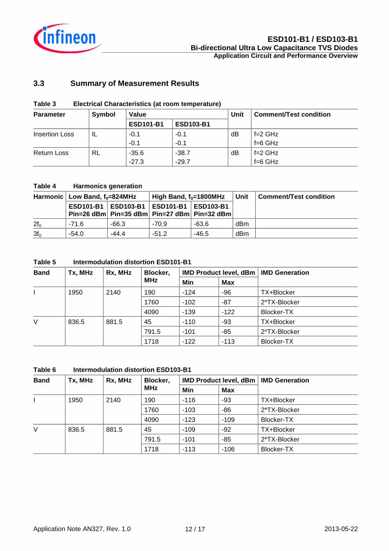
In order to measure insertion and return loss, devices were connected to a network analyzer as shown in Figure 8 without any additional modules in between. To minimize parasitic effects caused by PCB discontinuities, the full 2-port calibrated measurement was done with RF probes direct on the device pads. Insertion (IL) and return (RL) loss was calculated from measured data as follows:
21log20 SIL
11log20 SRL
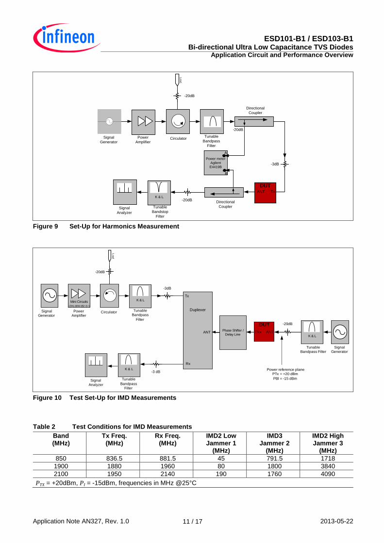
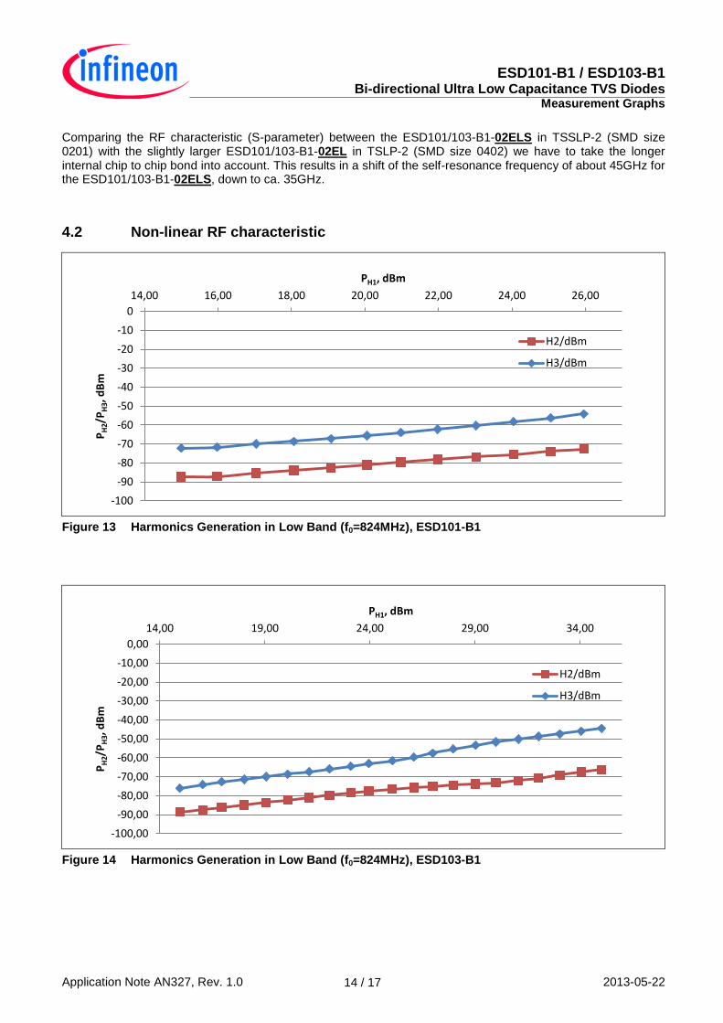
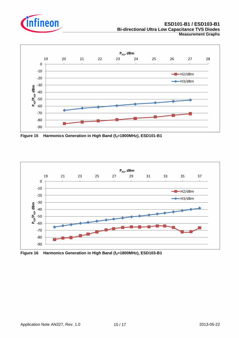
Non linear characterization of the ESD101/103-B1 is done via harmonic measurement P(H2), P(H3) at given fundamental power P(H1) and by the intermodulation distortion measurement for a given blocker and interferer constellation. Setups for nonlinearity measurements (harmonics and intermodulation distortion) are shown on Figure 9 and Figure 10 respectively. Mesurement results for the harmonics P(H2), P(H3) vs. fundamental power P(H1) are included in chapter 4.2.
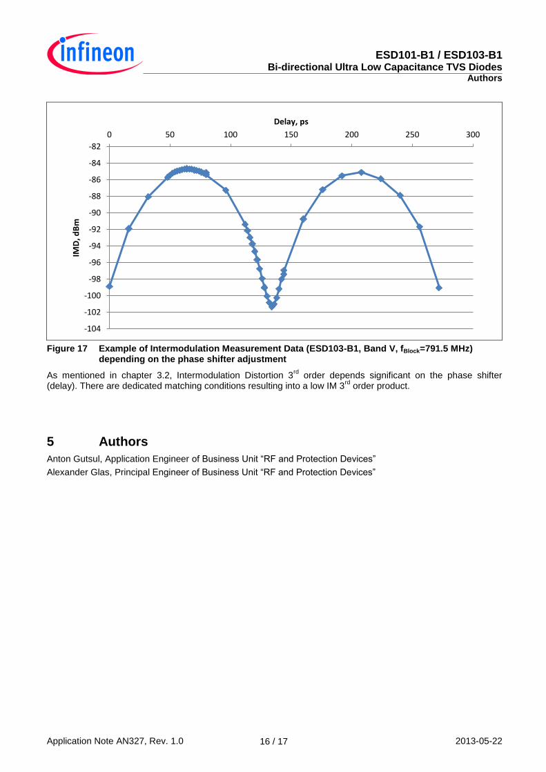
Intermodulation distortion (IMD) measurement reproduces more the scenario of real application. In this scenario (e.g. in all kind of full duplex systems like CDMA, UMTS, LTE) the high power transmission signal (Tx, e.g. PTX =20 dBm) and a received Jammer signal (e.g. PI =-15 dBm) are both entering the TVS diode. Special combinations of Tx and Jammer signals produce 2
nd and 3
rd order intermodulation products, which can fall in the
Rx band and interfere with the wanted Rx signal.
With the help of the phase shifter, matching conditions for the interfering signal can be adapted to simulate various matching scenario. Lowest intermodulation is expected at the ESD diode providing a low load impedance load for the blocker.
Test conditions for intermodulation measurements are summarized in paper from Nokia titled „Antenna Switch Linearity Requirements for GSM/WCDMA Mobile Phone Front-Ends” presented at the “Wireless Technolgies 2005 - 8th European Conference on Wireless Technology”.
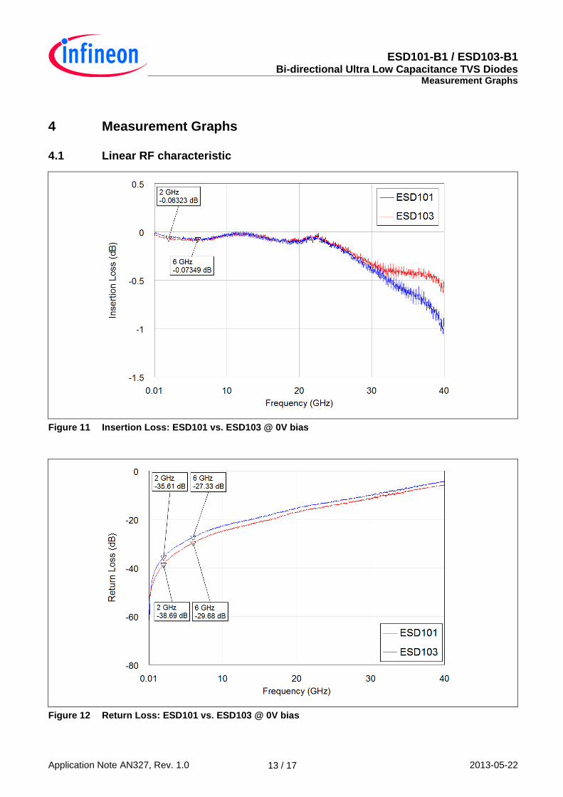
Comparing the RF characteristic (S-parameter) between the ESD101/103-B1-02ELS in TSSLP-2 (SMD size 0201) with the slightly larger ESD101/103-B1-02EL in TSLP-2 (SMD size 0402) we have to take the longer internal chip to chip bond into account. This results in a shift of the self-resonance frequency of about 45GHz for the ESD101/103-B1-02ELS, down to ca. 35GHz.
4.2 Non-linear RF characteristic
Figure 13 Harmonics Generation in Low Band (f0=824MHz), ESD101-B1
Figure 14 Harmonics Generation in Low Band (f0=824MHz), ESD103-B1