November 2012 Doc ID 023243 Rev 1 1/26 AN4121 Application note Poly-phase demonstration kit with the STPMC1 and STPMS2 Introduction This application note describes the poly-phase demonstration kit with the STPMC1 and STPMS2. The STPMC1 is a metering ASSP implemented in an advanced 0.35 μm BCD6 technology. The STPMC1 device works as an energy calculator in power line systems utilizing a Rogowski coil, current transformer, shunt or Hall current sensors. Used in combination with one or more STPMS2 ICs, it implements all the functions needed in a 1-, 2- or 3-phase energy meter, providing effective measurement of active and reactive energies, V RMS , I RMS , instantaneous voltage and current per phase in 1-, 2- or 3-phase wye and delta services, from 2 to 4 wires. In a standalone configuration, the STPMC1 outputs a pulse train signal having a frequency proportional to the cumulative active power, and it can directly drive a stepper motor, therefore implementing a simple active energy meter. This device can also be coupled with a microprocessor for multifunction energy meters. In this case, measured data are read at a fixed time interval from the device internal registers by the microcontroller through an SPI interface. The STPMS2 is an ASSP designed to be the building block for single or multiphase energy meters. It consists of a preamplifier and two 2 nd order Δ∑ modulators, band-gap voltage reference, a low-drop voltage regulator and DC buffers in its analog section and clock generator and output multiplexer in its digital section. The demonstration kit is made up of a main board with the STPMC1 onboard (STEVAL- IPE0010V1), and it can be coupled with up to 5 daughterboards, each having an STPMS2 onboard to sense the voltage and current of each phase (STEVAL-IPE0014V1). Figure 1. Demonstration kit block diagram AM12798v1 N R S T Cur r ent Sensor Vol t age Sensor STPMS2 S T PMS 2 S T PMS 2 S T PMS 2 STPMC1 DAR DAS DAH CLK XTAL1 XTAL2 VSS VSSA MOP MON VOT P VCC DAN DAT VDD SDA- TD S CL - NC S YN- NP SCS LED S T P M M M 2 S T P M M M 2 S T P M M M 2 P1 DAR DAT DAN DAH DAS www.st.com
Transcript
November 2012 Doc ID 023243 Rev 1 1/26
AN4121Application note
Poly-phase demonstration kit with the STPMC1 and STPMS2
IntroductionThis application note describes the poly-phase demonstration kit with the STPMC1 and STPMS2.
The STPMC1 is a metering ASSP implemented in an advanced 0.35 µm BCD6 technology.
The STPMC1 device works as an energy calculator in power line systems utilizing a Rogowski coil, current transformer, shunt or Hall current sensors. Used in combination with one or more STPMS2 ICs, it implements all the functions needed in a 1-, 2- or 3-phase energy meter, providing effective measurement of active and reactive energies, VRMS, IRMS, instantaneous voltage and current per phase in 1-, 2- or 3-phase wye and delta services, from 2 to 4 wires.
In a standalone configuration, the STPMC1 outputs a pulse train signal having a frequency proportional to the cumulative active power, and it can directly drive a stepper motor, therefore implementing a simple active energy meter.
This device can also be coupled with a microprocessor for multifunction energy meters. In this case, measured data are read at a fixed time interval from the device internal registers by the microcontroller through an SPI interface.
The STPMS2 is an ASSP designed to be the building block for single or multiphase energy meters. It consists of a preamplifier and two 2nd order Δ∑ modulators, band-gap voltage reference, a low-drop voltage regulator and DC buffers in its analog section and clock generator and output multiplexer in its digital section.
The demonstration kit is made up of a main board with the STPMC1 onboard (STEVAL-IPE0010V1), and it can be coupled with up to 5 daughterboards, each having an STPMS2 onboard to sense the voltage and current of each phase (STEVAL-IPE0014V1).
Figure 1. Demonstration kit block diagramAM12798v1N R S T
Poly-phase systems, and particularly three-phase meters, are most commonly used in practical industrial applications, and in a few cases also for domestic use.
The purpose of the STEVAL-IPE0010V1 + STEVAL-IPE0014V1 is STPMC1 and STPMS2 device demonstration but it can also be used as a starting point to design a Class 0.2 accuracy meter for power line systems from 2- to 4-wire delta or wye service.
Each phase is monitored from an independent daughterboard, in which an autonomous power supply provides the supply to the board itself and, once it is connected, also to the motherboard.
In this board, the STPMS2 device senses the phase current through a CT sensor, and the phase voltage through a voltage divider. The presence of a dedicated network reduces, for a large amount, the sampling (aliasing) noise, therefore increasing the meter precision. The STPMS2 outputs a sigma-delta stream sent, together with supply voltage, to the STPMC1 through a card edge connector.
The motherboard receives from the daughterboards the sigma-delta streams that are further elaborated by the STPMC1. This device, from a 4.194 MHz crystal oscillator, provides a common clock with programmable frequency to all the daughterboards.
The motherboard, through a 10-pin flat cable connector (P1 in Figure 2), can be interfaced to a microprocessor board to implement advanced metering features (multi-tariff, data management and storage, communication…). It also has stepper motor connectors for a simple energy meter implementation (W2, W5 in Figure 2).
The STPMC1 board can also be interfaced to a dedicated GUI through the STPMxx parallel programmer/reader released with the application.
Table 1. Operating conditions
Condition Value Unit
VNOM 230 VRMS
INOM CT: INOM = 1 ARMS
IMAX CT: IMAX = 30 ARMS
fLIN 50/60 ± 10% Hz
TOP - 40 / + 85 °C
AN4121 Circuit description
Doc ID 023243 Rev 1 5/26
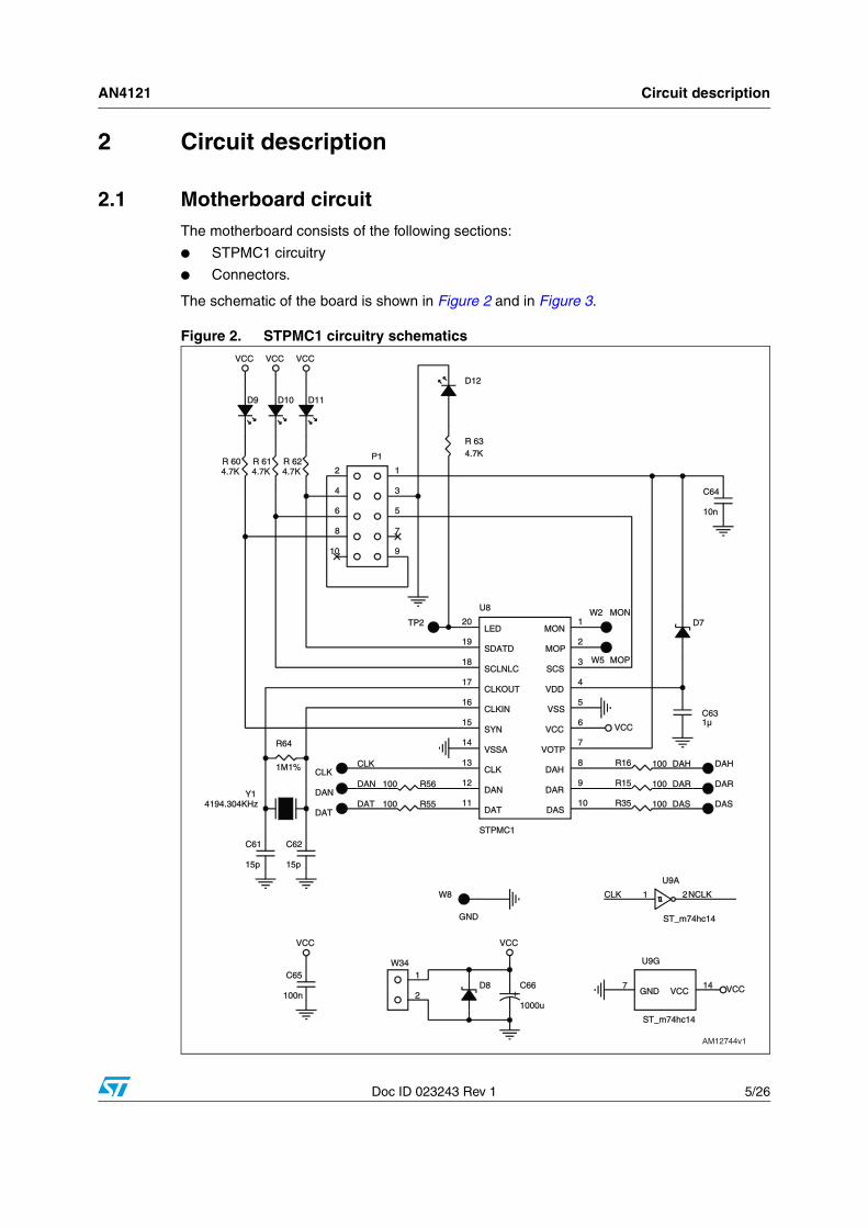
2 Circuit description
2.1 Motherboard circuitThe motherboard consists of the following sections:
● STPMC1 circuitry
● Connectors.
The schematic of the board is shown in Figure 2 and in Figure 3.
Figure 2. STPMC1 circuitry schematics
VCC
VCC VCC VCC
VCC
VCC
VCC
DAR
DASDAT
CLK
DAN
DAH
CLK NCLK
R 614.7K
U8
STPMC1
1
2
3
4
5
6
7
8
9
1011
12
13
14
15
16
17
18
19
20MON
MOP
SCS
VDD
VSS
VCC
VOTP
DAH
DAR
DASDAT
DAN
CLK
VSSA
SYN
CLKIN
CLKOUT
SCLNLC
SDATD
LED
R 624.7K
DAT
W341
2
W2 MON
W5 MOP
Y14194.304KHz
P1
1
5
910
8
6
4
2
3
7
U9A
ST_m74hc14
1 2
R56100
D7
+C66
1000u
R16 100
C631µ
TP2
C61
15p
C64
10n
R15 100DAN
R 604.7K
C65
100n
D10
DAH
R35 100
D11
R 634.7K
CLK
D8
D12
R55100
U9G
ST_m74hc14
7 14GND VCC
C62
15p
R64
1M1%
DAR
W8
GND
D9
DAS
AM12744v1
AN4121 Circuit description
Doc ID 023243 Rev 1 6/26
Figure 3. Motherboard connectors schematics
2.2 Daughterboard circuitThis section explains the implementation of each phase network which performs the power measurement.
The schematic can be divided into the following subsets:
● Current sensing circuit (1) or (2)
● Anti-aliasing filter (3)
● Voltage sensing circuit (4).
2.2.1 Current sensing circuit
The STPMS2 has an external current sensing circuit using either a current transformer, in which a burden resistor is used to produce a voltage between CIN and CIP proportional to the current measured, or a shunt resistor, or a Rogowski coil current sensor.
2.2.2 Anti-aliasing filter
The anti-aliasing filter is a low-pass filter. It has a negligible influence on the voltage drop between CIN and CIP, VIN and VIP; its aim is to reduce the distortion caused by the sampling, also called aliasing, by removing the out-of-band frequencies of the input signal before sampling it with the analog-to-digital converter.
Filtering is easily implemented with a resistor-capacitor (RC) single-pole circuit which obtains an attenuation of - 20 dB/dec.
2.2.3 Voltage sensing circuit
A resistor divider is used as voltage sensor.
The 660 kΩ resistor is separated into four, 2 x 150 kΩ and 2 x 180 kΩ, in-series resistors, which ensure that a high voltage transient does not bypass the resistor. This also reduces the potential across the resistors, thereby decreasing the possibility of arcing. The following resistors are used to implement resistor divider:
● R = R13 + R2 + R3 + R4 = 660 kΩ● R5 = 470 Ω.
Inductance L1 and capacitor C2 create a filter which prevents electromagnetic interference (EMI).
AM12745v1
VCC
VCC
VCC VCC
VCC VCC
NCLK
CLK
DAR DAS DAT
NCLK
CLK
NCLK
CLK
J1
Card_Edge_10
F1
F2
F3
F4
F5
F6
F7
F8
F9
F10
S1
S2
S3
S4
S5
S6
S7
S8
S9
S10
J2
Card_Edge_10
F1
F2
F3
F4
F5
F6
F7
F8
F9
F10
S1
S2
S3
S4
S5
S6
S7
S8
S9
S10
J3
Card_Edge_10
F1
F2
F3
F4
F5
F6
F7
F8
F9
F10
S1
S2
S3
S4
S5
S6
S7
S8
S9
S10
VCC VCC
VCCVCC
DAN DAH
NCLK
CLK
NCLK
CLK
J5
Card_Edge_10
F1
F2
F3
F4
F5
F6
F7
F8
F9
F10
S1
S2
S3
S4
S5
S6
S7
S8
S9
S10
J4
Card_Edge_10
F1
F2
F3
F4
F5
F6
F7
F8
F9
F10
S1
S2
S3
S4
S5
S6
S7
S8
S9
S10
AN4121 Circuit description
Doc ID 023243 Rev 1 7/26
Figure 4. Daughterboard circuit schematic
2.2.4 Jumper settings
The onboard jumpers JP1 to JP4 allow the setting of the STPMS2 device according to Table 2, Table 3, Table 4 and Table 5 below.
AM12799v1
Table 2. Precision mode and input amplifier gain selection
JP1 MS0 Description
1 GND LPR, amplifier GAIN selection g3 = 32
2 (1)
1. Default value.
CLK LPR, amplifier GAIN selection g0 = 4
3 NCLK HPR, amplifier GAIN selection g0 = 4
4 VDD HPR, amplifier GAIN selection g3 = 32
AN4121 Circuit description
Doc ID 023243 Rev 1 8/26
For further details on device configuration, please refer to its datasheet.
2.3 Clock management networkA 4.194 MHz quartz is used to supply the clock to the STPMC1 device. To set this frequency, internal configuration bits MDIV and FR1 must be kept cleared.
A synchronized clock is provided to all the STPMS2 through pin CLK, whose frequency is programmable through bit HSA to 1.049 MHz or 2.097 MHz.
2.4 Communication with microprocessorA control board with embedded microprocessor may be connected to connector P1 using 10-wire flat cable. Table 5 below describes the pinout of the connector.
The STPMC1 has an SPI communication port implemented by four multipurpose pins (SCS, SYN-NP, SDA-TD, SCL-NLC).
Table 3. TC of the band-gap reference
JP2 MS1 Description
1 GND TC = 60 ppm/°C
2 (1)
1. Default value.
CLK Flattest TC = +30 ppm/°C
3 NCLK TC = +160 ppm/°C
4 VDD TC = -160 ppm/°C
Table 4. Control of voltage channel and output signals
JP3 MS2 Description
1 (1)
1. Default value.
GND Voltage channel ON, DATn = ~(DAT =(CLK) ? bsV : bsC)
2 CLK Voltage channel OFF, DATn = bsCn, DAT = bsC
3 NCLK Voltage channel OFF, DATn = bsCn, DAT = bsC
4 VDD Voltage channel ON, DATn = bsC, DAT = bsV
Table 5. Changing of band-gap voltage reference
JP4 MS3 Description
1 (1)
1. Default value.
GND Hard mode, BIST mode OFF
2 CLK Soft mode
3 NCLK Reserved
4 VDD Hard mode, BIST mode ON
AN4121 Circuit description
Doc ID 023243 Rev 1 9/26
In standalone operating mode these multipurpose pins output:
● negative power direction on SYN-NP pin;
● tamper condition detected on SDA-TD pin;
● no load condition detected on SCL-NLC pin.
For this reason these pins are connected to the three LEDs, D9, D10 and D11.
In this configuration, the LED pin outputs a pulse train with frequency proportional to the three-phase power and it is connected to LED D12.
When configured in peripheral operating mode, the SPI port is enabled and some microcontroller based applications can either read internal data records or write the mode and configuration signals by means of dedicated protocol, or reset the device.
By default, the STPMC1 is configured in peripheral mode (configuration bits APL=0).
This also implies the following output settings:
● watchdog reset signal on MON pin;
● zero-crossing (ZCR) on MOP pin;
● programmable energy pulsed output on LED pin.
For further information on STPMC1 programmable bit settings, please refer to the datasheet.
The STPMC1 SPI protocol is explained in detail in a related application note.
Connector P1 is also used in the demonstration phase to connect the measurement module to a PC through the STPM parallel programmer/reader hardware interface.
This allows the user to set temporary and/or permanently the internal STPMC1 registers using a dedicated GUI.
The VOTP pin on the connector P1 is used when a host wants to permanently write some configuration bits in the STPMC1 device. In this case, a +15 V power level must be present on the VOTP. This level must be delivered from the host itself because the module does not have an onboard charge pump.
Table 6. P1 connector pin description
Pin Pin name Functional description
1. VOTP Power supply input of +15.0 V during permanent write to OTP cells
2. --- Not connected
3. GND Signal reference level 0 V and power supply return
4. SDA-TD SPI interface data
5. SCS SPI interface enable
6. SCL-NLC SPI interface clock
7. --- Not connected
8. SYN-NP SPI interface signal
9. --- Not connected
10. VCC Power-out of +3.3 or 5 V
AN4121 Board layout
Doc ID 023243 Rev 1 10/26
3 Board layout
3.1 Layout rules for three-phase systems designNoise rejection is the main issue to work on when a three phase multi-chip approach has been chosen. In this case layout plays a crucial role.
Here are some rules to follow in the layout phase of three-phase systems:
● Component positioning
The components of the measuring section (STPMS2, current sensor, passive components) should be placed using the same layout for each phase. The phases should be placed in a symmetrical scheme. In this way a reduction of the cross talking can be achieved.
The current sensor should be placed very close to the corresponding STPMS2 to minimize the captured noise.
● Component routing
The passive components belonging to the analog input channels must be placed between the sensor and the STPMS2, always respecting a symmetrical scheme.
● Quartz
The crystal network must be placed close to the STPMC1, and a completely symmetrical path from the CLK pin of the STPMC1 to STPMS2 devices must be ensured. A copper plate has been adopted under the crystal both on the TOP and on the BOTTOM side of the PCB.
● Grounding
The STPMS2 device must be grounded by the exposed pad and by pin VSS, ensuring the maximum stability of ground plane by placing vias between the top and bottom ground plane. Analog and digital ground must be separated.
3.2 Motherboard layout
Figure 5. Motherboard top layout
AN4121 Board layout
Doc ID 023243 Rev 1 11/26
Figure 6. Motherboard bottom layout
3.3 Daughterboard layout
Figure 7. Daughterboard top layout
AN4121 Board layout
Doc ID 023243 Rev 1 12/26
Figure 8. Daughterboard bottom layout
AN4121 Experimental results
Doc ID 023243 Rev 1 13/26
4 Experimental results
The tests have been conducted on a three-phase metering demonstration board with the STPMC1 and three STPMS2Ls considering INOM = 5 A, VNOM = 230 V, fline = 50 Hz.
Results are referred to the full scale dynamic range of the current channel (“FS” in Table 7), which for the sensor selected was ± 37.5%, or as percentage of INOM.
4.1 Three-phase energy measurement accuracy
4.1.1 Test with symmetrical voltages and balanced load at PF = 1
This three-phase energy measurement has been performed in the following conditions:
VR = VS = VT = 230 [VRMS]
IR = IS = IT = I [ARMS]
PF = 1
Table 7. Three-phase energy measurement
I [A] % of INOM [%] % of FS [%] error [%]
22,5 450% 100% 0,097%
16 320% 71% 0,076%
12 240% 53% 0,040%
10 200% 45% 0,035%
8 160% 36% -0,008%
5 100% 22% 0,027%
2 40% 9% 0,035%
1 20% 4% -0,065%
0,5 10% 2% -0,087%
0,25 5% 1% -0,096%
0,1 2% 0,4% -0,087%
0,05 1% 0,2% -0,096%
0,025 0,5% 0,1% -0,096%
0,01 0,2% 0,04% -0,352%
0,005 0,1% 0,02% -0,435%
0,0025 0,05% 0,01% -0,487%
AN4121 Experimental results
Doc ID 023243 Rev 1 14/26
Figure 9. Graph of experimental results of three-phase energy measurements
4.1.2 Test with symmetrical voltages and balanced load at PF = 0.5 inductive and PF = 0.8 capacitive
This three-phase energy measurement has been performed in the following conditions:
VR = VS = VT = 230 [VRMS]
IR = IS = IT = I [ARMS]
PF = 0.5 ind
PF = 0.8 cap
Table 8. Limits for class 0,2 meters: poly-phase meters with symmetrical voltages and balanced loads at PF = 1
I [A] % of INOM [%] error [%]
IMAX - ± 0,2%
In 100% ± 0,2%
0,05*In 5% ± 0,2%
0,0499*In 4,99% ± 0,4%
0,01*In 1% ± 0,4%
AM12746v1
0,076%
0,040%0,035%
-0,008%0,027%0,035%
-0,065%-0,087%-0,096%
-0,087%-0,096%-0,096%
-0,352%
-0,435%-0,487%
-0,6%
-0,5%
-0,4%
-0,3%
-0,2%
-0,1%
0,0%
0,1%
0,2%
0,3%
0,4%
0,5%
0,01% 0,10% 1,00% 10,00% 100,00%
AW E
rror [
%]
% of FS
Class 0.2 limits
AN4121 Experimental results
Doc ID 023243 Rev 1 15/26
Figure 10. Graph of experimental results of three-phase energy measurement
Table 9. Three-phase energy measurement - PF = 0.5 ind
I [A] % of INOM [%] % of FS [%] error [%]
12 240% 53% -0,1932%
10 200% 45% -0,1449%
8 160% 36% -0,1087%
5 100% 22% -0,1484%
2 40% 9% -0,0971%
1 20% 4% -0,1507%
0,5 10% 2% -0,0928%
0,25 5% 1% -0,0348%
0,1 2% 0,4% -0,1739%
0,05 1% 0,2% 0,0174%
Table 10. Three-phase energy measurement - PF = 0.8 cap
I [A] % of INOM [%] % of FS [%] error [%]
12 240% 53% 0,0393%
10 200% 45% 0,0525%
8 160% 36% 0,0861%
5 100% 22% 0,0362%
2 40% 9% 0,0634%
1 20% 4% 0,0435%
0,5 10% 2% 0,0362%
0,25 5% 1% 0,0652%
0,1 2% 0,4% 0,0725%
0,05 1% 0,2% 0,1812%
AM12747v1
-0,1932%
-0,1449%-0,1087%-0,1484%
-0,0971%-0,1507%
-0,0928%-0,0348%
-0,1739%
0,0174% 0,0393%
0,0525%0,0861%
0,0362%0,0634%0,0435%0,0362%0,0652%0,0725%0,1812%
-0,6%
-0,4%
-0,2%
0,0%
0,2%
0,4%
0,6%
1% 10% 100% 1000%
AW E
rror [
%]
% of In
Class 0.2 limit - PF = 0,5L/0,8CPF = 0,8C
PF = 0,5L
AN4121 Experimental results
Doc ID 023243 Rev 1 16/26
4.2 Typical phase energy measurement accuracy
4.2.1 Test with symmetrical voltages and only one phase load at PF = 1 and PF = 0,5 inductive
This single-phase energy measurement has been performed in the following conditions:
VR = VS = VT = 230 [VRMS]
IR = I [ARMS]
IS = IT = 0
PF = 1
PF = 0.5 ind
Table 11. Limits for class 0,2 meters: poly-phase meters with symmetrical voltages and balanced loads at PF = 0,5 ind or 0,8 cap
I [A] % of INOM [%] error [%]
IMAX - ± 0,3%
In 100% ± 0,3%
0,1*In 10% ± 0,3%
0,099*In 9,9% ± 0,5%
0,02*In 5% ± 0,5%
Table 12. Phase energy measurement
I [A] % of In [%] error [%]
10 200% -0,0003%
8 160% -0,0212%
5 100% -0,0426%
2 40% 0,1152%
1 20% -0,0309%
0,5 10% -0,0348%
0,2 4% 0,1196%
AN4121 Experimental results
Doc ID 023243 Rev 1 17/26
Figure 11. Graph of experimental results of one phase energy measurement
Table 13. Phase energy measurement PF = 0.5 inductive
I [A] % of In [%] error [%]
10 200% -0,2348%
8 160% -0,2565%
5 100% -0,2504%
2 40% -0,1870%
1 20% -0,2087%
0,5 10% -0,1217%
0,2 4% 0,0130%
Table 14. Limits for class 0,2 meters: poly-phase meters with symmetrical voltages and only one phase load at PF = 1
I [A] % of In [%] error [%]
IMAX 1000% ± 0,3%
0,05*In 5% ± 0,3%
Table 15. Limits for class 0,2 meters: poly-phase meters with symmetrical voltages and only one phase load at PF = 0.5 ind
I [A] % of In [%] error [%]
IMAX 1000% ± 0,4%
0,1*In 10% ± 0,4%
AM12748v1
-0,0003%-0,0212%
-0,0426%
0,1152%
-0,0309%-0,0348%
0,1196%
-0,2348%
-0,2565%-0,2504%
-0,1870%
-0,2087%
- 0,1217%
0,0130%
-0,5%
-0,4%
-0,3%
-0,2%
-0,1%
0,0%
0,1%
0,2%
0,3%
0,4%
0,5%
1% 10% 100% 1000%
AW
Err
or [%
]
% of In
Class 0.2 limit - PF = 0,5
Class 0.2 limit - PF = 1
PF = 0,5
PF = 1
AN4121 Three-phase systems
Doc ID 023243 Rev 1 18/26
Appendix A Three-phase systems
Three-phase is a common method of electric power transmission. It is a type of poly-phase system used to power motors and many other devices.
The currents are sinusoidal functions of time, all at the same frequency but with different phases. In a three-phase system the phases are spaced equally, giving a phase separation of 120°. The frequency is typically 50 Hz in Europe and 60 Hz in the US and Canada.
Figure 12. Instantaneous voltage (or current) in one voltage cycle of a three-phase system
The three phases may be supplied over six wires, with two wires reserved for the exclusive use of each phase. However, they are generally supplied over three or four wires:
● Three-phase, 3-wire delta service which has no neutral and 220 V between phases
● Three-phase, 4-wire delta and wye service which has 220 V between phase-neutral and 380 V phase-phase.
A.1 Power in three-phase AC circuitsLet's assume that the angle between the phase voltage and the phase current is θ, which is equal to the angle of the load impedance. Considering the load configurations given in Figure 14, the phase power and the total power can be estimated easily.
AN4121 Three-phase systems
Doc ID 023243 Rev 1 19/26
Figure 13. Per-phase powers in (a) a delta-connected load and (b) wye-connected load
In the case of Figure 13.a, the total active power is equal to three times the power of one phase:
Since the line current in the balanced delta-connected loads,
If this equation is substituted into equation 3.51, the total active load becomes:
Equation 1
In Figure 13.b, however, the impedances contain the line currents Iline (equal to the phase current, Iphase) and the phase voltages:
Therefore, the phase active power and the total active power are:
θ==== cosIVPPPP phaseline321
θ== cosIV3P3P phaselineTotal
phaseline I3I =
θ= cosIV3P linelineTotal
3VV linephase =
θ==== cosIVPPPP linephase321
θ== cosIV3P3P linephaseTotal
AN4121 Three-phase systems
Doc ID 023243 Rev 1 20/26
If the relationship between the phase voltage and the line voltage is used, the total active power becomes identical to Equation 1 developed. This means that the total power in any balanced three-phase load (θ- or Y-connected) is given by Equation 1.
Similarly, the total reactive and the total apparent power in the three-phase balanced AC circuits can be given by:
A.2 Power measurement techniquesIn the three-phase power systems, one, two, or three wattmeters can be used to measure the total power. A wattmeter may be considered to be a voltmeter and an ammeter combined in the same box, which has a deflection proportional to VrmsIrmscos θ, where θ is the angle between the voltage and current. Hence, a wattmeter has two voltage and two current terminals, which have + or θ polarity signs. Three power measurement methods utilizing the wattmeters are described next, and are applied to the balanced three-phase AC load.
A.2.1 Two-wattmeter method
This method can be used in a three-phase 3-wire balanced or unbalanced load system that may be connected θ or Y. To perform the measurement, two wattmeters are connected as shown in Figure 14.
Figure 14. Two-wattmeter method in star- or delta-connected load
In the balanced loads, the sum of the two wattmeter readings gives the total power. This can be proven in a star-connected load mathematically using the power reading of each meter as:
θ= sinIV3Q linelineTotal
linelineTotal IV3S =
AN4121 Three-phase systems
Doc ID 023243 Rev 1 21/26
If the difference of the readings is computed,
which is 1/√⎯3 times the total three-phase reactive power. This means that the two-wattmeter method can also indicate the total reactive power in the three-phase loads and also the power factor.
A.2.2 Three-wattmeter method
This method is used in a three-phase four-wire balanced or unbalanced load. The connections are made with one meter in each line as shown in Figure 15. In this configuration, the total active power supplied to the load is equal to the sum of the three wattmeter readings.
Figure 15. The wattmeter connections in the three-phase 4-wire loads
A.2.3 One-wattmeter method
This method is suitable only in three-phase 4-wire balanced loads. The connection of the wattmeter is similar to the drawing given in Figure 15. The total power is equal to three times the reading of only one wattmeter that is connected between one phase and the neutral.
Item Quantity Reference Part PCB Footprint Description
18 1 R10 2.2 M 1% sm_0603
19 1 R11 100 1% sm_0603
20 2 R14, R17 10 sm_0603
21 2 R15 or R16, R18 0 sm_0603
22 1 SH1 170 µ r_shunt
23 1 SH2 170 µ r_shunt_2
24 1 TR1 E4622_X503 VAC_e4622_x503
25 1 U1 STPMS2Lmcs_manual_mlp3x3_16_05_pa
d
26 1 V1 460 V disc_450x200_ls300x100_037 VARISTOR MOKS K10*300V
27 1 W1 N TEST_POINT
28 1 W2 F TEST_POINT
29 1 W3 DAR TEST_POINT
30 1 W4 VREG TEST_POINT
31 2 W5, W8 VCC TEST_POINT
32 1 W6 GND TEST_POINT
33 1 W7 CLK TEST_POINT
Table 17. Daughterboard BOM list (continued)
AN4121 Revision history
Doc ID 023243 Rev 1 25/26
5 Revision history
Table 18. Document revision history
Date Revision Changes
06-Nov-2012 1 Initial release.
AN4121
Doc ID 023243 Rev 1 26/26
Please Read Carefully:
Information in this document is provided solely in connection with ST products. STMicroelectronics NV and its subsidiaries (“ST”) reserve theright to make changes, corrections, modifications or improvements, to this document, and the products and services described herein at anytime, without notice.
All ST products are sold pursuant to ST’s terms and conditions of sale.
Purchasers are solely responsible for the choice, selection and use of the ST products and services described herein, and ST assumes noliability whatsoever relating to the choice, selection or use of the ST products and services described herein.
No license, express or implied, by estoppel or otherwise, to any intellectual property rights is granted under this document. If any part of thisdocument refers to any third party products or services it shall not be deemed a license grant by ST for the use of such third party productsor services, or any intellectual property contained therein or considered as a warranty covering the use in any manner whatsoever of suchthird party products or services or any intellectual property contained therein.
UNLESS OTHERWISE SET FORTH IN ST’S TERMS AND CONDITIONS OF SALE ST DISCLAIMS ANY EXPRESS OR IMPLIEDWARRANTY WITH RESPECT TO THE USE AND/OR SALE OF ST PRODUCTS INCLUDING WITHOUT LIMITATION IMPLIEDWARRANTIES OF MERCHANTABILITY, FITNESS FOR A PARTICULAR PURPOSE (AND THEIR EQUIVALENTS UNDER THE LAWSOF ANY JURISDICTION), OR INFRINGEMENT OF ANY PATENT, COPYRIGHT OR OTHER INTELLECTUAL PROPERTY RIGHT.
UNLESS EXPRESSLY APPROVED IN WRITING BY TWO AUTHORIZED ST REPRESENTATIVES, ST PRODUCTS ARE NOTRECOMMENDED, AUTHORIZED OR WARRANTED FOR USE IN MILITARY, AIR CRAFT, SPACE, LIFE SAVING, OR LIFE SUSTAININGAPPLICATIONS, NOR IN PRODUCTS OR SYSTEMS WHERE FAILURE OR MALFUNCTION MAY RESULT IN PERSONAL INJURY,DEATH, OR SEVERE PROPERTY OR ENVIRONMENTAL DAMAGE. ST PRODUCTS WHICH ARE NOT SPECIFIED AS "AUTOMOTIVEGRADE" MAY ONLY BE USED IN AUTOMOTIVE APPLICATIONS AT USER’S OWN RISK.
Resale of ST products with provisions different from the statements and/or technical features set forth in this document shall immediately voidany warranty granted by ST for the ST product or service described herein and shall not create or extend in any manner whatsoever, anyliability of ST.
ST and the ST logo are trademarks or registered trademarks of ST in various countries.
Information in this document supersedes and replaces all information previously supplied.
The ST logo is a registered trademark of STMicroelectronics. All other names are the property of their respective owners.
Australia - Belgium - Brazil - Canada - China - Czech Republic - Finland - France - Germany - Hong Kong - India - Israel - Italy - Japan - Malaysia - Malta - Morocco - Philippines - Singapore - Spain - Sweden - Switzerland - United Kingdom - United States of America