The purpose of this document is to give an overview on how to derive the Si446x RFIC family's receiver settings tocomply with ETSI EN 300 220-1 category 1 Rx specifications in narrowband (<25 kHz) applications.
2. The Standard
Table 1 lists the specifications a receiver must meet for Category 1 compliance:
The most popular frequency bands where Category 1 receivers operate at (from ETSI EN 300 220-1).
Table 1. Receiver Specifications for Category 1 Compliance
Parameter ETSI limit Unit Comment
Sensitivity –107 dBm
LBT Threshold NA NAonly applications with LBT (Listen Before Talk) protocol
ACS 54 dB channel spacing < 25 kHz
Saturation ACS 44 dB channel spacing < 25 kHz
Blocking 84 dB At 2 MHz and 10 MHz offset
Spurious Response 60 /35 dBspec gets relaxed to 35 if spurious is within 0.1 % of the wanted tone, channel spacing < 25 kHz
Spurious Radiation 2/20 nW below and above 1 GHz
Notes:1. All parameters refer to an Rx BW of 16 kHz. If a different BW is used the limits have to be compensated by
the following factor 10log10(RxBW[kHz]/16). The limits get relaxed by this much when BW is wider than 16 kHz.
2. Specs for channel spacing > 25 kHz are not included in the table.
Table 2. Popular Frequency Bands for Category 1 Receivers
Frequency Bands/Frequencies
Applications Maximum Radiated Power, E.R.P. / Power Spectral
Density
Channel Spacing Spectrum Access and Mitigation Requirement
(e.g. Duty cycle or LBT + AFA)
169.475 MHz to 169.4875 MHz
Social Alarms 10 mW 12.5 kHz 0.10%
169.5875 MHz to 169.6000 MHz
Social Alarms 10 mW 12.5 kHz 0.10%
869.200 MHz to 869.250 MHz
Social Alarms 10 mW 25 kHz 0.10%
AN736
2 Rev 0.2
3. 868 MHz Solution with SAW Filter
In this section all of the parameters are considered for an ETSI category 1 compliant receiver solution in the 868MHz frequency band. At this frequency of operation additional filtering is required in front of the RFIC’s input ason its own the receiver would not comply with the blocking specification. See the details in the following sections.
3.1. Blocking
The table contains the mean and standard deviation values of the 2 MHz blocking numbers at varioustemperatures. The values in the last row of the table can be considered as worst case numbers.
It is clearly seen that these numbers fall short of the specification outlined in section 2, therefore additionalfiltering—practically in the form of a SAW filter—is required in front of the receiver input. After the bandwidthcompensation (on the 12.4 kHz filter) the specification is 85.1 dB. Comparing this number with numbers in the lastrow of the table it can be calculated that 10 dB attenuation at 2 MHz offset will make all the parts pass thespecification.
The following table contains the 10 MHz blocking results from the same characterization run.
Following the same logic as before a minimum attenuation of 5 dB is required from the selected SAW filter at
10 MHz offsets.
Modulation format: 2GFSK 3kbps DR with 3 kHz singe sided deviation
Receive BW: 12.4 kHz
Center frequency: 869.2125 MHz
Mode of operation: BER testing mode
Table 3. 2 MHz Blocking Results at 869.2125 MHz
2MHz blocking -40 °C 25 °C 85 °C
Mean [dB] -77,5 -77,64 -77,82
Stdev [dB] 0,34 0,31 0,36
Mean + 3 stdev [dB] -76,5 -76,7 -76,7
Mean + 6 stdev [dB] -75,5 -75,8 -75,7
Notes:1. The wanted signal power level during the blocking test is defined by ETSI as –107 dBm + 10*log10 (12.4 [kHz]/16 [kHz})
[dB] + 3 [dB] = –105.1 dBm. At this particular test this level was dropped further by 2.8 dB—the typical insertion loss of a SAW filter in the 868 MHz band—to –107.9 dBm to “simulate” how much power the receiver would see at its input port in a real application.
2. These blocking numbers have been collected with optimized AGC configuration to keep the spread down. For details, refer to section 3.1.2.
Table 4. 10 MHz Blocking Results at 869.2125 MHz
10 MHz blocking -40 °C 25 °C 85 °C
Mean [dB] -85,02 -87,08 -87,26
Stdev [dB] 0,82 1,09 0,32
Mean + 3 stdev [dB] -82,56 -83,81 -86,3
Mean + 6 stdev [dB] -80,1 -80,54 -85,34
AN736
Rev 0.2 3
3.2. Spurious Response RejectionETSI calls for testing selectivity at three particular offset frequencies where spurious responses may occur.
These frequencies are the image frequency of the receiver and the +/- IF/2 (Intermediate Frequency) offsetfrequencies from the wanted channel. At +/- IF/2 offset there is no spurious response; the selectivity performanceis purely limited by phase noise on the receive LO (Local Oscillator). Therefore this sub-section focuses only onimage selectivity.
The IF frequency in the recommended mode of operation in the 868 MHz frequency band is 406.25 kHz. The LO isof a low injection type, i.e. it is running one IF frequency below the wanted receive band. The IF frequency iscalculated as 1/64th of the reference frequency (XO/TCXO). This calculation yields the IF frequency stated abovewith the recommended 26 MHz reference source in the 868 MHz frequency band. The image frequency is at twotimes the IF frequency below the wanted frequency.
The following table summarizes the image selectivity results taken on Si446x revC2 RFICs over process variationand supply voltage. IQ calibration was activated on the parts.
Note that worst case numbers (last row in the table) are estimated with using only three times the standarddeviation “guarding” the average. The reason for applying this method is that the distribution of the measurementresult is not Gaussian; it is more like a Ryleigh distribution which is much “harder limited” at the lower (i.e worseperformance) section than at the higher end. See the distribution of the measurement results on below CCDF(Complementary Cumulative Distribution Function) plot.
Figure 1. Image Selectivity Distribution at 869.2125 MHz
Even though the spread is relatively high on the data set it is driven by measured points taking on much bettervalues than the average (rather than much worse). In other words the result of the calibration can be arbitrarilygood but cannot be arbitrarily bad. You can read more on IQ calibration in AN790.
The worst case estimate numbers in the table would fail the 60 dB specification set out in the standard, however aswith the recommended configuration (26 MHz TCXO) the image frequency falls within 0.1% of the wanted
Table 5. Image Selectivity Distribution at 869.2125 MHz
Image Selectivity -40 C 25 C 85 CMean [dB] 47.16 48.68 50.06
Stdev [dB] 3.23 2.86 4.59
Mean - 3 stdev [dB] 37.5 40.1 36.3
AN736
4 Rev 0.2
frequency a 25 dB relaxation applies to the specification that brings it down to 35 dB which in turn will be met on allparts with the IQ calibration feature enabled. Note also, that most SAW filters will have some attenuation at theimage frequency that will also increase the margin on the specification.
3.3. Adjacent Channel SelectivityAdjacent Channel Selectivity (selectivity at +/- 25 kHz offset) is a rather tough specification. Care must be taken tooptimize the receiver for the best performance. ACS depends on a number of factors:
1. Selectivity/attenuation performance of Rx filter
2. PLL phase noise performance at the given offset
3. Demodulator SNR requirement for error-free detection
#1 can be optimized by selecting an Rx filter with the best attenuation at the adjacent channel. #2 can be optimizedby selecting a PLL bandwidth resulting in the least integrated phase noise power in the adjacent channel. #3 canbe optimized by selecting more robust modulation formats. (This latter one cannot be applied if the modulationformat is fixed.) In the following sub-section all above three points are elaborated on.
3.3.1. Rx Filter Selection
The Rx filter has finite attenuation at the adjacent channel (+/-25 kHz), therefore some of the signal energy at thisoffset will still reach the detector block deteriorating so the receive performance. While phase noise is a muchbigger contributor to ACS it is still desirable that a filter be selected that has the best attenuation at +/- 25 kHzoffset. The best filters from this aspect are the 12.4 kHz and the 16.53 kHz wide ones given that therecommended 26 MHz TCXO is used. They both have approximately the same bandwidth compensated ACSperformance. That is to say the 16.53 kHz filter has a 1 dB weaker ACS. The limit, however, is relaxed by 1 dBcompared to the 12.4 kHz filter case.
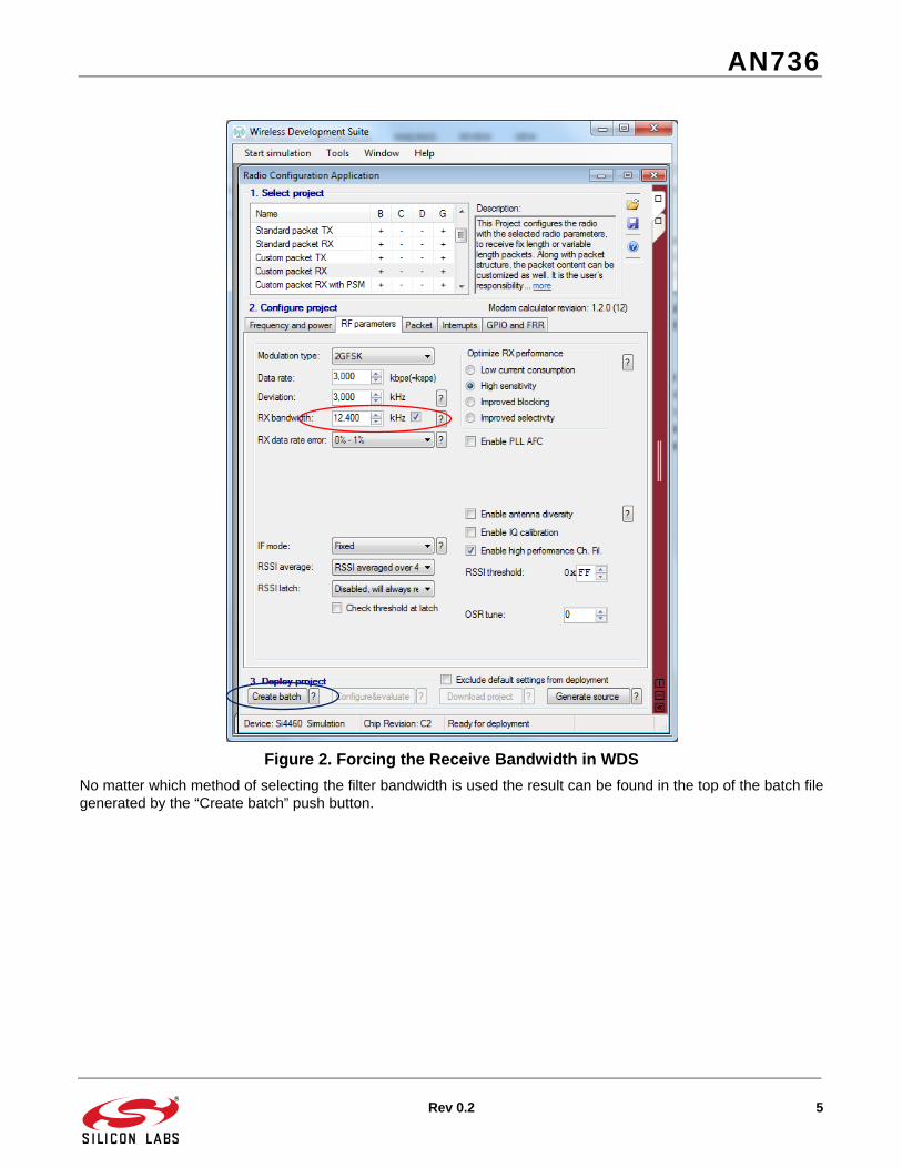
In WDS there are two ways of calculating the receive filter bandwidth. It can either be calculated by WDSautomatically based on the modulation parameters on the “RF parameters” tab and the crystal toleranceparameters on the “Frequency and power” tab, or it can be forced by the user if the checkbox next to the “Rxbandwidth” entry field is ticked. In this latter case WDS will select the closest possible (higher) filter bandwidthregardless of the rest of the input parameters. See below a WDS screenshot on how to force the receive filterbandwidth.
AN736
Rev 0.2 5
Figure 2. Forcing the Receive Bandwidth in WDS
No matter which method of selecting the filter bandwidth is used the result can be found in the top of the batch filegenerated by the “Create batch” push button.
AN736
6 Rev 0.2
Figure 3. Checking the Selected Filter Bandwidth in WDS
3.3.2. PLL Phase Noise Optimization
Changing the bandwidth (typically opening it up) of the PLL has the effect of re-shaping the noise profile in a waythat close-in phase noise gets better at the price of some further-out noise degradation. See below graph on howmuch improvement can be realized at 25 kHz offset by gradually opening up the bandwidth of the PLL.
AN736
Rev 0.2 7
Figure 4. Close-In Phase Noise Improvement with PLL BW Increase
There is approximately 2 dB improvement going from the default 200 kHz to 300 kHz and there is an additional 1dB gain if the 400 kHz configuration is selected. Note, that simultaneously 2 MHz phase noise degrades by roughlyas much too. However, the data in section 3.1 was already taken with the 400 kHz PLL bandwidth configuration sothe conclusion on the 2 MHz attenuation of the SAW filter (10 dB) is still valid.
The RCA (Radio Control Application) in WDS does not provide for direct PLL bandwidth adjustment. However if“Improved Selectivity” is chosen from the “Optimize Rx performance” selection control on the “RF parameters tab”the 400 kHz bandwidth PLL configuration will be selected. On how to make the various PLL BW configurations takeeffect manually refer to section 5. The “improved selectivity” option is primarily devised for 868 MHz band ETSIcategory 1 applications therefore there are a couple of more “behind the scenes” actions that further optimize theperformance.
Field “ETSI_MODE” in API property MODEM_IF_CONTROL is set to a value of 1. The effect of this value is optimized close-in phase noise performance on the PLL. (On chip revision revB1B this optimization was done through a direct register access POKE command, on chip revision revC2 this is automatically done by the FW.) Note that even though this field resides in an IF related property it has no effect whatsoever on the IF configuration.
Optimized AGC switching points will be set via API property “MODEM_IFPKD_THRESHOLDS”. This action is needed to keep the variation down on the 2 MHz blocking numbers.
The following WDS screenshot shows how to enable the “Improved selectivity” option.
AN736
8 Rev 0.2
Figure 5. Activating Optimized Rx Performance for 868 MHz Band ETSI Category 1 Applications
As the most limiting factor on ACS performance is phase noise on the receive LO it is important that the selectedreference source’s (26 MHz TCXO) own phase noise (that directly appears on the LO too) is at least 10 dB betterthan performance of the synthesizer itself. If this criterion is met than the phase noise of the reference source willnot have a degrading effect on ACS. The required phase noise specification on the reference source is -147dBc/Hz at 25 kHz offset. This number is calculated (see figure below) as the synthesizer’s phase noise at 25 kHzoffset at 869 MHz (-107 dBc/Hz) “downconverted” to 26 MHz (20*log10 (869/26)) and taking away the 10 dBmargin.
The mechanisms described in the previous two sections (finite filter attenuation / mixing on phase noise) have theeffect of unwanted signal energy—aka noise—appearing at the demodulator circuitry. Now how much of this noisethe demodulator can tolerate before it starts making wrong decisions (in other words what is the least SNR—Signal to Noise Ratio—requirement for successful demodulation) does change with the modulation parameters.Typically the demodulator is more tolerant to noise if the modulation index is higher. The frequency symbols arefurther apart from one another in this case (in other words the eye opening is bigger) therefore more noise isneeded to “smear” the two symbols together. The receiver’s ACS performance thus will be proportional to thedemodulator’s least SNR requirement.
Typically the receiver’s ACS will get better if higher modulation indices are used and as long as the modemis running in asynchronous mode, ACS will also get better if the data rate is dropped at a given modulation index. Ifthe modem, however, is operating in synchronous mode, ACS will not change with the data rate at any givenmodulation index. On modem operation and AFC (Automatic Frequency Control) considerations, please refer toAN734.
As a system’s design aid, find below a few sets of curves showing exactly how ACS and sensitivity change withdata rate and deviation. The data has been taken at 869.2125 MHz applying all the phase noise enhancementmeasures detailed in the previous section (“Improved Selectivity” has been ticked in WDS). Data is shown for thetwo filter settings (12.4 kHz and 16.53 kHz) that yield the best ACS performance. The graphs also show the(bandwidth compensated) specifications as solid red lines. (Beware that sensitivity numbers are referred to the 50ohm connector of the pico board; they will be degraded by the insertion loss (~3 dB) of the SAW filter.)
AN736
10 Rev 0.2
Figure 7. Sensitivity vs Data Rate 12.4 kHz Rx Filter
Figure 8. ACS vs Data Rate 12.4 kHz Rx Filter
AN736
Rev 0.2 11
Figure 9. Sensitivity vs Data Rate 16.53 kHz Rx Filter
Figure 10. ACS vs Data Rate 16.53 kHz Rx Filter
AN736
12 Rev 0.2
3.3.4. ACS Statistical Analysis
The following table summarizes ACS results in the 868 MHz frequency band on 20 pieces of Si446x revC2 RFICover process variation and supply voltage at room temperature. The parts were configured the following way:
At this particular modulation format the worst case ACS result (modeled by the last row of the table) still meets the-55 dB specification. Note that the part the detailed sweeps were taken on in the previous sub-section wellrepresents the average of the population. The data point on figure Figure 8, “ACS vs Data Rate 12.4 kHz Rx Filter,”on page 10 at 3kbps DR and a modulation index of 2 matches well with the average result in this table. So if othermodulation formats are chosen simply shift the results in this table by as much as the measurement results differon the detailed graphs.
With increasing data rates and lower modulation indices the population of parts may not meet the specificationstatistically. If the 12.4 kHz wide filter is selected try to stay below 3 kbps DR with a modulation index ofgreater than or equal to 2. If the 16.53 kHz wide filter is selected try to stay below 4 kbps DR with amodulation index of greater than or equal to 2.
3.4. SummaryThere are a few restrictions that must be adhered to for building an ETSI category1 compliant receive application inthe 868 MHz band with the Si446x RFIC family.
Keep the DR below 4 kbps and maximize the modulation index
Enable the “Improved Selectivity” Rx operation mode in WDS
Use a 26 MHz TCXO with at least as good an accuracy as +/- 2.5 ppm and as good a phase noise as -147 dBc/Hz at 25 kHz offset
Enable IQ calibration on the chip
Use one of the recommended Rx filters from section 3.1.1
Use a SAW filter in front of the receiver’s input with the following specification
As far as the reference accuracy is concerned if one assumes an Rx BW of 12.53 kHz the best AFC range the partcan provide is +/- 4.38 kHz (see AN734 for details) which split between Rx and Tx equally (+/- 2.19 kHz) yields areference accuracy requirement of 2190 [Hz] / 869 [MHz] = 2.52 [ppm]. This sort of accuracy requirement can only
Modulation format: 2GFSK 3kbps DR with 3 kHz single sided deviation
Receive BW: 12.4 kHz
Center frequency: 869.2125 MHz
Mode of operation: BER testing mode with “Improved selectivity” option
Table 6. ACS Results at 869.2125 MHz
ACS at +/- 25 kHz 25 °C
Mean [dB] -59,82
Stdev [dB] 0,73
Mean + 3 stdev [dB] -57,63
Mean + 6 stdev [dB] -55,44
Table 7. 868 MHz Band SAW Filter Specification
868M SAW spec +/- 2MHz +/- 10MHz
Attenuation [dB] 10 5
AN736
Rev 0.2 13
be met with TCXOs.
For development purposes and radio performance evaluation order the following radio pico board:4463CPCE20C869SE. This picoboard comes with an EPCOS B3749 SAW filter and a TX0341E +/- 2.5 ppm 26MHz TCXO from Tai-Saw Technology (TST).
Figure 11. 4463CPCE20C869SE
4. 169 MHz Solution without a SAW Filter
In this section all of the parameters are considered for an ETSI category1 compliant receiver solution in the 169MHz frequency band. At this frequency of operation no additional filtering is required in front of the receiver input.
4.1. BlockingThe following table summarizes narrowband blocking results in the 169 MHz frequency band both at 2 MHz and10 MHz offsets. The data were taken on 10 pieces of Si446x revC2 RFIC at room temperature and nominal 3.3 Vsupply voltage. The parts were configured the following way:
Modulation format: 2GFSK 3kbps DR with 3 kHz single sided deviation
Receive BW: 10.65 kHz
Center frequency: 169 MHz
Mode of operation: BER testing mode with “Improved selectivity” option
Table 8. Blocking Results at 169 MHz
25 C
Blocking 2 MHz 10 MHz
Mean [dB] -87,32 -87,92
Stdev [dB] 0,13 0,21
Mean + 3 stdev [dB] -86,9 -87,3
Mean + 6 stdev [dB] -86,5 -86,7
AN736
14 Rev 0.2
The table contains the mean and standard deviation values of the 2 MHz and 10 MHz blocking numbers. Thevalues in the last row of the table can be considered as worst case numbers at room temperature.
As the spread is very little on the data room temperature worst case numbers are only slightly worse than theaverage and still meet the bandwidth compensated specification of 85.8 dB.
In order to achieve the blocking numbers above that make the use of a SAW filter unnecessary the “Improvedblocking” checkbox must be selected at “Optimize RX performance” control on the “RF parameters” tab in WDS.See the control on the below WDS screenshot.
Figure 12. Enabling the “Improved Blocking” Operation Mode in WDS
There are several actions taken if the “Improved Blocking” mode of Rx operation is selected. Field “ETSI_MODE”in API property MODEM_IF_CONTROL is set to a value of 2 that has the following implications on the part.
The AGC (Automatic Gain Control) algorithm is optimized to always withstand -20 dBm blocker power level while maintaining enough gain in the system to still meet the ETSI defined sensitivity specification.
The mixer is placed in “high linearity” mode. Note that this mode of mixer operation will increase overall receive current consumption by ~ 300 uA.
The bandwidth of the analog baseband will be set to its minimum value of 375 kHz to provide more attenuation at the blocker frequencies. Note that this mode of operation makes the use of SIF (Scaled IF) mode recommended. If FIF (Fixed IF) mode were used the IF frequency (at 468.75 kHz assuming a 30 MHz reference
AN736
Rev 0.2 15
source) would already be attenuated by the baseband filter. This mechanism would lead to a few dB sensitivity loss. (Another requirement that makes the SIF mode operation not only recommended but mandatory is the spurious response specification. See section 4.2 for details.)
4.2. Spurious Response RejectionCalibrated image selectivity numbers at 169 MHz are the same as at 868 MHz. From section 3.2 it is clearly seenthat the specification is only met if the 25 dB relaxation is applied to the 60 dB limit. For the relaxation to take effecta sufficiently low IF frequency (<84.5 kHz) is required to keep the image frequency within 0.1% of the wantedfrequency itself. It follows than that SIF (Scaled IF) mode has to be utilized on the part as in FIF (Fixed IF) modethe IF frequency would be way higher than the maximum allowed for the specification relaxation. Note, that ZIF(Zero IF) mode would get rid of the image frequency entirely, it would come, however at a price of a few (~3) dBsensitivity degradation and more susceptibility to low frequency noise. So while the specification would still be metin ZIF mode, SIF is the recommended mode of operation for better overall performance.
In scaled IF mode of Rx operation by default the image frequency falls onto the (lower) adjacent channel (from thechannel filter’s bandwidth point of view). There is a way of scaling the IF frequency upwards by stepping thesampling clock frequency higher in the demodulator. This scaling can be achieved by increasing the OSRtune(Over Sampling Ratio tune) value on the “RF parameters” tab in WDS. While the exact oversampling ratio cannotbe set it can be stepped up (as well as down) with regards to the nominal value by changing the OSRtune control.The resulting IF frequency is shown in the batch and radio configuration header files right below the Rx BW value.Now, as the default IF frequency places the image frequency on the lower adjacent channel (from the channelfilter’s bandwidth point of view) it will obviously degrade the ACS performance therefore a higher IF frequency isrecommended to be used. Increasing the IF frequency, however has a degrading effect on Rx filter selectivity. (Thereason for this is that increasing the IF frequency is achieved by upscaling the sampling clock in the digitaldemodulator, which in turn makes it necessary that a different digital filter be selected whose relative bandwidth willbe lower which fundamentally results in less sharper a roll off at the filter’s edges.) Experiments have shown thatthe best compromise between above two factors is an OSRtune value selection of 3. The WDS screenshot belowshows how to configure Scaled IF mode with the aforementioned OSRtune value of 3.
AN736
16 Rev 0.2
Figure 13. Configuring Scaled IF (SIF) Mode From WDS
AN736
Rev 0.2 17
This particular configuration with a forced RX bandwidth of 10 kHz and an OSRtune value of 3 the IF frequency is19.531 kHz. The image frequency therefore is 39.062 kHz below the wanted frequency. For information find belowhow the IF frequency changes with OSRtune value at this particular configuration.
4.3. Adjacent Channel SelectivityAdjacent channel selectivity in the 169 MHz is not as critical as in the 868 MHz band. The main limiting factor onACS is phase noise on the receive LO at a frequency offset equal to the channel spacing. Phase noise isfundamentally better at 169 MHz by a factor of 20 x log10(868M/169M) = 14.2 [dB] at any given offset frequency.Therefore there is no need for configuration optimization for meeting the ACS specification in the 169 MHzfrequency band.
4.4. SummaryThere are a few restrictions that must be adhered to for building an ETSI category1 compliant narrowband receiveapplication in the 169 MHz band with the Si446x RFIC family.
Enable the “Improved Blocking” Rx operation mode in WDS
Configure Scaled IF Rx operation with an OSRtune value of 3
Enable IQ calibration on the chip
Use the recommended 30 MHz XO/TCXO
Note that while in the 868 MHz band a TCXO is always recommended in the 169 MHz band a conventional XOmay as well be used as long as its accuracy is at least as good as +/-10 ppm. If one assumes a 10 kHz Rx BW(that is typical in the 169 MHz band) the best AFC range the part can offer is +/- 3.5 kHz (see AN734 for details)which split equally between Rx and Tx (+/- 1.75 kHz) yields an accuracy requirement of 1750 [Hz] / 169 [MHz] =10.35 ppm.
For development purposes and RF performance evaluation order any of the following pico boards:
4463CPSQ20D169TRx board
4362CPRXB169Rx only board
Table 9. IF Frequency vs OSRtune Value
OSRtune IF [Hz]
-2 3662
-1 4883
0 7324
1 9766
2 14648
3 19531
4 29297
Note: Access to OSR tune is locked by license in WDS (3.2.7.0onwards) for advanced users. Contact Silicon Labs should youneed this feature to be activated.
AN736
18 Rev 0.2
4.5. PLL BW configurationsThere are multiple API properties involved in modifying the bandwidth of the PLL. For the sake of completenessfind here the settings for all mentioned (200 kHz - default, 300 kHz and 400 kHz) cases.
# Synth control group = 200 kHz Loop BW
'SET_PROPERTY' 'SYNTH_PFDCP_CPFF' 2C
'SET_PROPERTY' 'SYNTH_PFDCP_CPINT' 0E
'SET_PROPERTY' 'SYNTH_VCO_KV' 0B
'SET_PROPERTY' 'SYNTH_LPFILT3' 04
'SET_PROPERTY' 'SYNTH_LPFILT2' 0C
'SET_PROPERTY' 'SYNTH_LPFILT1' 73
'SET_PROPERTY' 'SYNTH_LPFILT0' 03
# Synth control group = 300 kHz Loop BW
'SET_PROPERTY' 'SYNTH_PFDCP_CPFF' 34
'SET_PROPERTY' 'SYNTH_PFDCP_CPINT' 04
'SET_PROPERTY' 'SYNTH_VCO_KV' 0B
'SET_PROPERTY' 'SYNTH_LPFILT3' 04
'SET_PROPERTY' 'SYNTH_LPFILT2' 07
'SET_PROPERTY' 'SYNTH_LPFILT1' 70
'SET_PROPERTY' 'SYNTH_LPFILT0' 03
# Synth control group = 400 kHz Loop BW
'SET_PROPERTY' 'SYNTH_PFDCP_CPFF' 14
'SET_PROPERTY' 'SYNTH_PFDCP_CPINT' 07
'SET_PROPERTY' 'SYNTH_VCO_KV' 0B
'SET_PROPERTY' 'SYNTH_LPFILT3' 02
'SET_PROPERTY' 'SYNTH_LPFILT2' 10
'SET_PROPERTY' 'SYNTH_LPFILT1' 73
'SET_PROPERTY' 'SYNTH_LPFILT0' 03
Any of these settings can be made to take effect if the corresponding property values are manually overwritten tothese values in the radio configuration header file.
AN736
Rev 0.2 19
4.6. Recommended External Components for ETSI Category 1 ComplianceThis section contains recommended external components for ETSI Category 1 compliance.
Table 10. Recommended Reference Source Parts
Manufacturer Part number Operating Frequency [MHz] Temperature range [°C ]
TST TX0338A 30 -30 - 75
TST TXO341E 26 -40 - 85
Table 11. Recommended SAW Filters at 869 MHz
Manufacturer Part number Center Frequency
[MHz]
Operating band [MHz]
Temperature range [°C ]
EPCOS B3749 869,3 868,6-870 –10 to 55
TST TA0275A 869,6 869,12-870,26 –45 to 90
RFM SF2280E 869.2125868.6125-869.8125
–10 to 55
EPCOS B3941 868,95 868,7-869,2 –45 to 85
EPCOS B3746 868,6 868-869,2 –45 to 95
http://www.silabs.com
Silicon Laboratories Inc.400 West Cesar ChavezAustin, TX 78701USA
Smart. Connected. Energy-Friendly.
Productswww.silabs.com/products
Qualitywww.silabs.com/quality
Support and Communitycommunity.silabs.com
DisclaimerSilicon Labs intends to provide customers with the latest, accurate, and in-depth documentation of all peripherals and modules available for system and software implementers using or intending to use the Silicon Labs products. Characterization data, available modules and peripherals, memory sizes and memory addresses refer to each specific device, and "Typical" parameters provided can and do vary in different applications. Application examples described herein are for illustrative purposes only. Silicon Labs reserves the right to make changes without further notice and limitation to product information, specifications, and descriptions herein, and does not give warranties as to the accuracy or completeness of the included information. Silicon Labs shall have no liability for the consequences of use of the information supplied herein. This document does not imply or express copyright licenses granted hereunder to design or fabricate any integrated circuits. The products are not designed or authorized to be used within any Life Support System without the specific written consent of Silicon Labs. A "Life Support System" is any product or system intended to support or sustain life and/or health, which, if it fails, can be reasonably expected to result in significant personal injury or death. Silicon Labs products are not designed or authorized for military applications. Silicon Labs products shall under no circumstances be used in weapons of mass destruction including (but not limited to) nuclear, biological or chemical weapons, or missiles capable of delivering such weapons.
Trademark InformationSilicon Laboratories Inc.® , Silicon Laboratories®, Silicon Labs®, SiLabs® and the Silicon Labs logo®, Bluegiga®, Bluegiga Logo®, Clockbuilder®, CMEMS®, DSPLL®, EFM®, EFM32®, EFR, Ember®, Energy Micro, Energy Micro logo and combinations thereof, "the world’s most energy friendly microcontrollers", Ember®, EZLink®, EZRadio®, EZRadioPRO®, Gecko®, ISOmodem®, Precision32®, ProSLIC®, Simplicity Studio®, SiPHY®, Telegesis, the Telegesis Logo®, USBXpress® and others are trademarks or registered trademarks of Silicon Labs. ARM, CORTEX, Cortex-M3 and THUMB are trademarks or registered trademarks of ARM Holdings. Keil is a registered trademark of ARM Limited. All other products or brand names mentioned herein are trademarks of their respective holders.