UG:017 vicorpower.com Applications Engineering: 800 927.9474 Page 1 Introduction The Analog Control 3623 and 4623 ChiP DCM evaluation boards described in this document are designed to be used with the DCM family of isolated, DC-DC converters. The 3623 DCM board is used for the analog control, low input voltage 3623 ChiP products, while the 4623 DCM board is used for the analog control, high input voltage (offline) 4623 ChiP products. The DCM evaluation board can be configured for various enabling and fault monitoring schemes, as well as to exercise various modes of trimming, depending on the application requirements. The evaluation board can be used to evaluate DCMs in either a stand-alone configuration, or as an array of modules. Enable options: 1. On-board mechanical switch (default) 2. External control Trim options: 1. Fixed trim operation (default): the TR pin is permitted to float at initial startup. The DCM disables output trimming and the output trim is programmed to the nominal rated V OUT . 2. Variable trim operation, on-board variable resistor: The trim pin voltage is ratiometric, with a rheostat working against a pull-up resistor inside the DCM to VCC. 3. Variable trim operation, off-board control: The trim pin voltage is controlled via external programming control, which is referenced to the –IN of each specific DCM in the system. Fault monitor options: 1. On-board LED: the FT pin drives a visible LED for visual feedback on fault status. 2. On-board optocoupler: the FT pin drives an on-board optocoupler to bring fault status across the primary-secondary isolation boundary. Analog Control 3623 and 4623 ChiP DCMs Evaluation Board USER GUIDE | UG:017 Arthur Russell VI Chip ® Applications Engineering October 2014 Contents Page Introduction 1 Contents 3 Features 3 Board Description 4 General Components 4 Test Points Description 6 Schematic, Assembly Drawing and Bill of Materials 7 Recommended Test Equipment 14 Basic Connections 14 Board Operation Details 14 Trim Control 15 Fault Monitoring 15 Chassis Ground 16 Paralleling 16
The Analog Control 3623 and 4623 ChiP DCM evaluation boards described in this document are designed to be used with the DCM family of isolated, DC-DC converters. The 3623 DCM board is used for the analog control, low input voltage 3623 ChiP products, while the 4623 DCM board is used for the analog control, high input voltage (offline) 4623 ChiP products.
The DCM evaluation board can be configured for various enabling and fault monitoring schemes, as well as to exercise various modes of trimming, depending on the application requirements. The evaluation board can be used to evaluate DCMs in either a stand-alone configuration, or as an array of modules.
Enable options:
1. On-board mechanical switch (default)
2. External control
Trim options:
1. Fixed trim operation (default): the TR pin is permitted to float at initial startup. The DCM disables output trimming and the output trim is programmed to the nominal rated VOUT.
2. Variable trim operation, on-board variable resistor: The trim pin voltage is ratiometric, with a rheostat working against a pull-up resistor inside the DCM to VCC.
3. Variable trim operation, off-board control: The trim pin voltage is controlled via external programming control, which is referenced to the –IN of each specific DCM in the system.
Fault monitor options:
1. On-board LED: the FT pin drives a visible LED for visual feedback on fault status.
2. On-board optocoupler: the FT pin drives an on-board optocoupler to bring fault status across the primary-secondary isolation boundary.
Analog Control 3623 and 4623 ChiP DCMsEvaluation Board
USER GUIDE | UG:017
Arthur RussellVI Chip® Applications EngineeringOctober 2014
Contents Page
Introduction 1
Contents 3
Features 3
Board Description 4
General Components 4
Test Points Description 6
Schematic, Assembly Drawing and Bill of Materials 7
Hazardous voltages are present on the DCM Evaluation Board under power.
PERSONAL CONTACT WITH LINE VOLTAGE MAY RESULT IN SEVERE INJURY, DISABILITY, OR DEATH. IMPROPER OR UNSAFE HANDLING OF THIS BOARD MAY RESULT IN SERIOUS INJURY OR DEATH.
Read the precautions below entirely BEFORE using the DCM Evaluation Board. Do not operate the evaluation board unless you have the appropriate safety precautions in place on your bench to guarantee safety.
The list below is not comprehensive and is not a substitute for common sense and good practice.
nn During operation, the power devices and surrounding structures can be operated safely at high temperatures.
nn Remove power and use caution when connecting and disconnecting test probes and interface lines to avoid inadvertent short circuits and contact with hot surfaces.
nn Never use a jumper in place of the fuse.
nn When testing electronic products always use approved safety glasses. Follow good laboratory practice and procedures.
nn Avoid creating ground loops when making measurements of the isolated input or output voltage.
nn Care should be taken to protect the user from accidental contact when under power.
nn Care should be taken to avoid reversing polarities if connecting to the opposite (solder) side of the board.
nn The product evaluation boards described in this document are designed for general laboratory evaluation, and are not suitable for installation in end user equipment.
nn Refer to the specific DCM module data sheet for electrical, thermal, and mechanical product details
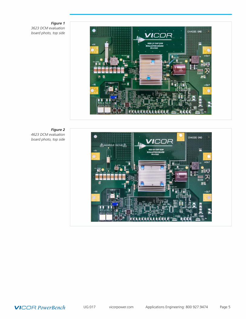
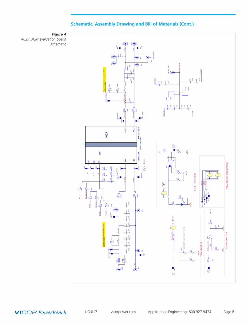
These boards provide a convenient way to evaluate/demonstrate the performance of Vicor’s DCM products. Kelvin connections are provided for accurate voltage measurements on power nodes. Sockets are provided to permit quick installation and changing of bulk filtering capacitors. The evaluation board also provides lugs for input/output connections, test points and sockets for easy connection to standard test-equipment, and a high performance air cooled heatsink assembly.
Contents
The evaluation board arrives with the following contents:
nn 1 x DCM evaluation board
nn 1 x top and belly heatsink assembly (pre-installed)
nn 1 x hardware kit
Features
The DCM evaluation board has the following features:
1. Input and output lugs for source and load connections
2. Input fuse (appropriately rated)
3. Basic input filtering, including sockets to add through-hole input aluminum-electrolytic capacitors for additional source decoupling
Note: The filtering used in the eval board is for demonstration purposes only and might not be the optimal solution for all applications. For optimal filter design for parallel array application, consult the datasheet of the DCM in use and the online filter design tool at:http://app2.vicorpower.com/filterDesign/intiFilter.do
4. Basic output filtering, including sockets to add through-hole output aluminum-electrolytic capacitors
5. Toggle switch for enabling and disabling the DCM via the ENABLE pin
6. Trim control selection
a. Using potentiometer
b. Using external voltage source
c. Open, to disable trimming and latch the model nominal trim condition
7. Provisions to replace input and output differential mode inductors with wire loops, for oscilloscope/shunt based current measurements
8. Oscilloscope probe jack for accurate, high frequency output voltage measurements
9. Dual paralleling connectors for ENABLE, TRIM, FAULT and SGND signal connections, for daisy chaining control to other DCM evaluation boards in an array
The following section provides a detailed description of the evaluation board components, test points and sockets.
General Components
1. DCM (PS01)
2. Input lugs: Sized for #10 hardware. Use these for making connection to the input source. This board does not contain reverse polarity protection. Check for proper polarity before applying the power.
3. Input fuse (F01 & F02): Appropriately rated for the DCM model on the board.
4. Input filter: Ceramic input capacitors (C15-C22), filtering inductor (L01) and damping resistor (R08) provide input filtering. Sockets (H01-H02, H03-H04) can be used for easy installation of aluminum-electrolytic input capacitors. The 3623 board also adds H09-H10 for additional input bypassing.
5. Enable / Disable switch (SW01): When actuator is in top position towards “ON” text on the board, the ENABLE pin will be open and the DCM will be enabled. When actuator is in bottom position towards “OFF” text on the board, the ENABLE pin will be connected to SGND and the DCM will be disabled. When switch SW01 is ON, an external voltage source can control the ENABLE state.
6. Header-jumper for trim control (J09): Provides the option to enable the trim function to set the DCM programmed trim value via either the on board trim rheostat or an external voltage source:
a. Using potentiometer (R26)
b. Using external voltage source.
7. Output lugs: Sized for #10 hardware. Use these lugs to connect the output directly to the load.
8. Output oscilloscope probe Jack (J01): Used for making accurate scope measurements of the output voltage (e.g. ripple). The jack is directly compatible with many common passive voltage probes models. Remove the grounding lead and insulating barrel of the probe and insert the probe tip and barrel directly into the jack, ensuring that the probe tip seats in the center socket of the jack. To avoid the risk of an inadvertent short circuit, do not attempt to install while power is applied.
9. Output filter: Output capacitor (C201), filtering inductor (L02) and damping resistors (R16-R17), and ceramic output capacitors (C02-C05) provide output filtering. Sockets H05-H06, and H03-H04 can be used for easy installation of aluminum-electrolytic output capacitors.
10. High side current sense wire loops: By depopulating the associated inductor and damping resistors, all input or output currents can be passed through a wire loop or use with an oscilloscope current probe. The wire loop is installed at the large pair of plated through-holes near the applicable inductor location.
11. Dual paralleling wire-to-board connectors (J02 and J03): Used for bussing control signals and their reference (ENABLE, SHARE, FAULT, and SGND) across board assemblies during parallel operation. The connector style provides simple “strip and insert” use with 18 – 24 AWG solid wires. Once inserted, a spring loaded barb retains each wire with no need for soldering. To release the wire, insert a thin bladed tool (AVX 06-9276-7001-01-000 or similar) into the slot above each wire entry point.
Schematic, Assembly Drawing and Bill of Materials: (Cont.)
General BOM rules for various DCM Evaluation Boards
nn PS01: This is the Vicor DCM, whose part number is coded in the evaluation board part number. For example, eval board DCM4623ED2K53E0M00 uses DCM4623TD2K53E0M00.
nn F01: This is the input fuse. See the datas heet for the specific DCM for appropriate fuse needed to meet listed safety agency approvals.
nn C201: This is the external output capacitor for the DCM. It is an Aluminum electrolytic with value that satisfies the DCM datasheet COUT-TRANS minimum.
The following is a list of recommended test equipment.
1. Safety glasses
2. DC power supply: Refer to the specific DCM model datasheet to ensure the supply has sufficient power and current capability, especially at low line, to satisfy current inrush when the DCM is started
3. Electronic load: Refer to the specific DCM model datasheet to ensure the load has sufficient power handling and current capability for testing
4. Cooling fan
5. Digital multi-meters (DMMs)
6. Oscilloscope and probes
7. Function generator
8. Auxiliary bench voltage supply (optional, for bias of secondary side fault monitor opto-coupler)
9. Interconnect wires, cables and fastening hardware
10. Calibrated input and output shunts, appropriately rated
11. Thin bladed tool for extracting wires from paralleling connectors (AVX 06-9276-7001-01-000 or similar)
Basic Connections
nn Confirm bench equipment is powered off.
nn Connect the input DC power supply positive lead to the +IN input lug of the evaluation board, connect the input power supply negative lead to the –IN input lug of the evaluation board.
nn Connect the CHASSIS_GROUND lug of the evaluation board to a safety “green wire” earth ground.
nn Connect the +OUT lug of the evaluation board to the electronic load positive input, connect the –OUT lug of the evaluation board to the electronic load negative input.
nn Direct airflow from the cooling fan through the DCM heatsink fins.
nn Have the latest DCM datasheet on hand for reference.
Board Operation Details
nn SW01 provides control over enable.
nn In the “OFF” position, the switch will connect SG the EN net, which disables the DCM.
nn In the “ON” position, SG is disconnected from the EN net.
nn External connection to EN is permitted using the PRI_EN testpoint. SW01 should be set to “ON” to permit external control.
nn The J02 & J03 paralleling connectors can be used to connect EN nets across different boards. Note: to enable the DCMs in a parallel array, all boards need SW01 set to “ON” to avoid pulling the EN node low.
nn With no jumpers installed, neither the trim potentiometer nor the test point for external trim con-trol is connected to the TR net. Note that the paralleling connectors always connect to the TR net.
nn With a jumper loaded across J09.1 and J09.2, the trim potentiometer R26 is connected as a rheostat between the TR node and SG.
nn With a jumper loaded across J09.3 and J09.4, the external trim test point is connected to the TR node.
nn The DCM contains an internal pull-up resistor to VCC (3.3V nominal). When VIN is applied to the DCM it samples the TR node voltage. If it has pulled up to VCC, the DCM disables trimming as long as it has input power, and the programmed trim condition will be nominal rated VOUT of the DCM model.
nn If the TR node is not permitted to pull-up to VCC when VIN is applied, trimming is enabled for as long as the DCM has input power.
nn Note: Any load on the TR node may cause the DCM to select trim mode when VIN is applied, including: the external trim testpoint (if selected with the jumper block), the trim potentiometer (if selected with the jumper block), and other DCM evaluation boards attached to the paralleling connectors.
nn The trim potentiometer adds a variable resistance between the TR node and SG, from between 0Ω nominal, to the value of the potentiometer (500kΩ). This resistance range will generate TR pin voltages which cover the entire functional range of the TR pin. Care should be taken to ensure the programmed trim condition is within the rated trim range of the DCM in order for the DCM to meet specifications.
nn In a parallel setup using the J02 & J03 paralleling connectors, all boards besides the top one should have the trim jumper select block at J09 open.
nn In a parallel setup with multiple DCM evaluation boards, each DCM contributes another internal pull-up resistor to a 3.3V nominal rail. With any resistive based trimming of the TR node, the resultant trim condition will be modified by the number of DCMs which are attached and have VIN applied. Conversely with a voltage source applied to the TR node, adding additional DCMs to the system has minimal impact on the resultant trim condition.
Fault Monitoring
nn Jumper block J10 configures how the FT node is monitored.
nn With no jumpers installed, neither the visible LED nor the opto-coupler is connected to the FT net. Note that the paralleling connectors always connect to the FT net.
nn With a jumper loaded across J10.3 and J10.4, the visible LED at D01 and its bias resistor network R09 & R32 are connected to the FT node.
nn With a jumper loaded across J10.1 and J10.2, the opto-coupler at M02 and its bias resistor net-work R21 & R22 is connected to the FT node.
nn The DCM FT output is intended to be directly paralleled with the FT output of other DCMs in an array. The FT node in an array forms a “wired-OR”, where any DCM can drive the FT node high.
nn Both the visible LED and the opco-coupler draw current from the FT node in a fault condition. The FT pin on the DCM has limited drive-high capabilities, and so care must be taken to avoid excess loading of the pin. To avoid overload, do not configure J10 to use both the LED and opto-coupler indicators simultaneously. When connecting external circuitry or test equipment to the FT test point, ensure that the maximum load on the FT node is within the DCM datasheet ratings.
nn In a parallel setup using the J02 & J03 paralleling connectors, all boards besides the top one should have the fault jumper select block at J10 open.
nn When using the opto-coupler, the status of the FT node can be easily transferred to the secondary side of the DCM(s) isolation boundary. To resolve the fault state on the secondary side, the collector side of the opto requires a bias voltage. A 5V bench supply should be connected between the “+5V” and “SEC_SG” testpoints. With no fault present, “FT_SEC” will be at 0V, and when a fault occurs and the opto-coupler is active, “FT_SEC” will pull up to 5V, relative to SEC_SG.
Chassis Ground
The heatsink assembly of the DCM is connected to the CHASSIS_GND node of the board, as well as the y-caps from each power connection of the DCM. A connection from the CHASSIS_GND lug to earth ground is required.
Paralleling
The paralleling and sharing performance of multiple DCMs can be easily demonstrated by stacking multiple evaluation boards and interconnecting the inputs and outputs with standoffs to create a parallel array. The DCM uses a negative load-line to implement wireless droop-sharing in an array. Each DCM in an array operates in the same way as it does as a stand-alone unit. With equal trim conditions, the load is effectively shared across multiple DCMs. Mismatches in this case are modest, and are further canceled by an effective negative voltage vs. temperature coefficient. See the DCM datasheet for more detail on load line and tempco. DCMs in an array require no derating of maximum output power or current.
DCMs in an array with mismatched trim conditions will not share the load equally at light- to moderate-load conditions. As the load increases, one or more DCMs (starting with those with the highest programmed output trim voltage) will go into current limit and their contribution to the overall output current will plateau. For DCMs, current limit is not a fault condition, rather it is a valid constant-current mode of operation and a DCM in current limit will provide constant current to the load. As long as the load does not exceed the maximum load rating of the array of DCMs, the output voltage will continue to be regulated by any remaining DCMs still in constant voltage mode. Even with mismatched trim conditions, the array can be safely loaded up to the full rated array capacity.
The following connections and settings should be used for an array of DCM evaluation boards:
nn All DCMs in a parallel array must be the same model.
nn The boards should be physically stacked using metal standoffs at the +IN & –IN lugs, the +OUT & –OUT lugs, and the CHASSIS_GND lug. This also connects these nodes electrically so that a single source, single load, and earth ground connection can be made to the system.
nn The +IN lugs are not required to be connected together for an array of DCMs. The wireless sharing does not require the same differential input voltage be present on all DCMs in the array. In some applications dissimilar input voltages may be needed, which is fully supported.
nn The –IN lugs must be connected together if the paralleling connector is used, or if the EN, TR, or FT pins are interconnected in any fashion. However if all control signals of all DCMs are fully isolated from one another, then both the +IN and –IN lugs can remain independent across the evaluation boards, and the DCMs can be operated with fully independent input supplies.
nn Standoffs must be sufficient in length to avoid contact between boards, and to permit airflow to all DCMs in the system.
nn If coordinated enable control, trimming or fault monitoring is desired, then the paralleling connectors J09 & J10 can be used to easily interconnect the PRI_FT, PRI_EN, PRI_TR_ and PRI_FT nodes across boards.
The paralleling connectors at J02 & J03 can be used for coordinated enable and trim control and fault monitoring. The enable, trim and fault monitor features of the top most board should be used for convenience, while the remaining boards should have their jumper blocks depopulated and enable switches set to enable.
The paralleling wire-to-board connectors (at J02 and J03) are provided to daisy chain control signals and PRI_SG, with a simple strip and insert option. They will accept 18 – 24 AWG solid wires.
Figure 7 DCM evaluation boards stacked
to form a high power parallel array, using common -IN and
the paralleling connectors.
Information furnished by Vicor is believed to be accurate and reliable. However, no responsibility is assumed by Vicor for its use. Vicor components are not designed to be used in applications, such as life support systems, wherein a failure or malfunction could result in injury or death. All sales are subject to Vicor’s Terms and Conditions of Sale, which are available upon request.
Specifications are subject to change without notice.