A forum for the exchange of circuits, systems, and software for real-world signal processing • Volume 49, Number 3, 2015 Analog Dialogue analog.com/analogdialogue Editor’s Notes; New Product Introductions Four Quick Steps to Production: Using Model-Based Design for Software-Defined Radio Part 1—the Analog Devices/Xilinx SDR Rapid Prototyping Platform: Its Capabilities, Benefits, and Tools New Advances in Energy Harvesting Power Conversion A Low Power Data Acquisition Solution for High Temperature Electronics Applications Analyzing, Optimizing, and Eliminating Integer Boundary Spurs in Phase-Locked Loops with VCOs at up to 13.6 GHz Interleaving ADCs: Unraveling the Mysteries Zero-Drift Amplifiers: Now Easy to Use in High Precision Circuits 2 3 10 13 19 22 27
Transcript
A forum for the exchange of circuits systems and software for real-world signal processing bull Volume 49 Number 3 2015
Analog Dialogue
analogcomanalogdialogue
Editorrsquos Notes New Product Introductions
Four Quick Steps to Production Using Model-Based Design for Software-Defined Radio Part 1mdashthe Analog DevicesXilinx SDR Rapid Prototyping Platform Its Capabilities Benefits and Tools
New Advances in Energy Harvesting Power Conversion
A Low Power Data Acquisition Solution for High Temperature Electronics Applications
Analyzing Optimizing and Eliminating Integer Boundary Spurs in Phase-Locked Loops with VCOs at up to 136 GHz
Interleaving ADCs Unraveling the Mysteries
Zero-Drift Amplifiers Now Easy to Use in High Precision Circuits
2
3
10
13
19
22
27
Analog Dialogue Volume 49 Number 32
Editorrsquos NotesIN THIS ISSUE
Four Quick Steps to Production Using Model-Based Design for Software-Defined Radio
Part 1mdashthe Analog DevicesXilinx SDR Rapid Prototyping
Platform Its Capabilities Benefits and Tools
This article series examines the advances in platforms and tools that allow developers to quickly simulate and prototype wireless radio systems while establishing and maintaining a deployable path to production As a real-world walkthrough of the process the authors will design and prototype a wireless SDR platform that receives and decodes ADS-B aircraft signals In this first part the article discusses the Analog DevicesXilinxreg SDR prototyping system its capabilities and benefits and a brief description of the tool flow (Page 3)
New Advances in Energy Harvesting Power Conversion
Today many power management integrated circuits are available that were specifically designed for use in energy harvesting applications They enable systems to run with smaller harvesters or make energy harvesting solutions possible that could not have been designed a few years ago This article looks at several energy harvesting applications and describes a high efficiency dc-to-dc conversion and voltage regula-tion solution that solves energy harvesting challenges (Page 10)
A Low Power Data Acquisition Solution for High Temperature Electronics Applications
A growing number of applications require data acquisition systems that must operate reliably at very high ambient environments such as downhole oil and gas drilling avionics and automotive This article presents a new reference design for high temperature data acquisition characterized from room temperature to 175degC (Page 13)
Analyzing Optimizing and Eliminating Integer Boundary Spurs in Phase-Locked Loops with VCOs at up to 136 GHz
A phase-locked loop (PLL) and voltage controlled oscillator (VCO) outputs an RF signal at a certain frequency and ideally this signal would be the only signal present at the output In reality there are unwanted spurious signals and phase noise at the output This article discusses the simulation and elimination of one of the more trouble-some spurious signalsmdashinteger boundary spurs (Page 19)
Interleaving ADCs Unraveling the Mysteries
Time interleaving is a technique that allows the use of multiple identical analog-to-digital converters to process regular sample data series at a faster rate than the operating sampling rate of each individual data converter This technique is frequently utilized in military and electronic instrumentation applications where there is a need to continually push the state-of-the-art in data conversion speeds resolutions and perfor-mance This article explains the data converter interleaving technique in technical detail as well as focusing on some of the practical challenges associated with implementing this technique (Page 22)
Zero-Drift Amplifiers Now Easy to Use in High Precision Circuits
A zero-drift amplifier as the name suggests is an amplifier with offset voltage drift very close to zero It uses auto-zero or chopping technology or a combination of both to continuously self-correct for dc errors over time and temperature This enables the amplifier to achieve microvolt level offsets and extremely low offset drifts making it uniquely suited for signal conditioning circuits that require high gain and precision performance This article explores the architecture of zero-drift ampli-fiers and provides insight into considerations for designing with these precision devices in drift-critical applications (Page 27)
Jim Surber [jimsurberanalogcom]
Product Introductions Volume 49 Number 3Data sheets for all ADI products can be found by entering the part number in the search box at analogcom
July
50 mA500 mA high efficiency ultralow power step-down regulator ADP5301
1 MSPS ultralow power 12-bit ADC in 10-lead LFCSP and MSOP AD7091R-5
31 W filterless class-D digital input audio amplifierSSM3515
Robust quad-channel isolator with input disable and 0 reverse channels ADuM140DADuM140E
Low power 400 MHz Blackfin+ embedded processor with 256 kB L2 SRAM ADSP-BF702
Low power 400 MHz Blackfin+ embedded processor with 512 kB L2 SRAM ADSP-BF704
Low power 400 MHz Blackfin+ embedded processor with 1 MB L2 SRAM ADSP-BF706
Isolated precision gate driver 4 A output ADuM3123
Robust triple-channel isolator with input disable and 0 reverse channels ADuM130D
Robust triple-channel isolator with input disable and 1 reverse channel ADuM131D
Ultracompact 1 A thermoelectric cooler (TEC) driver for digital control systems ADN8833
Ultracompact 15 A thermoelectric cooler (TEC) controller ADN8834
Single-dual-supply high voltage isolated IGBT gate driver with miller clamp ADuM4135
18 V 12 A step-down regulator with programmable current limit ADP2389
18 V 12 A step-down regulator with programmable current limit and PFM ADP2390
800 mA dc-to-dc inverting regulator ADP5075
Integrated precision battery sensors for automotive systems ADuCM330ADuC331
Analog DialogueAnalog Dialogue wwwanalogcomanalogdialogue the technicalmagazine of Analog Devices discusses products applications technology and techniques for analog digital and mixed-signal processing Published continuously for 49 yearsmdashstarting in 1967mdashit is available in two versions Monthly editions offer technical articles timely information including recent application notes circuit notes new- product briefs webinars and published articles and a universe of links to important and relevant information on the Analog Devices website wwwanalogcom Printable quarterly issues and ebook versions feature collections of monthly articles For history buffs the Analog Dialogue archive wwwanalogcomlibraryanalogdialoguearchiveshtml includes all regular editions starting with Volume 1 Number 1 (1967) and three special anniversary issues To subscribe please go to wwwanalogcomlibraryanalogdialoguesubscribehtml Your comments are always welcome Facebook wwwfacebookcomanalogdialogue EngineerZone ezanalogcomblogsanalogdialogue Email dialogue editoranalogcom or Jim Surber Editor [jimsurberanalogcom]
Analog Dialogue Volume 49 Number 3 3
Four Quick Steps to Production Using Model-Based Design for Software-Defined Radio Part 1mdashthe Analog DevicesXilinx SDR Rapid Prototyping Platform Its Capabilities Benefits and Tools
By Di Pu Andrei Cozma and Tom Hill
Abstract
There is a significant gap between the concept of a wireless system and the realization of that working design Bridging this gap typically involves teams of engineers with a variety of different skill sets (such as RF SW DSP HDL and embedded Linuxreg) and in many cases projects get derailed early in the development stage because of the difficulty in coordinating the efforts of these varied design entities
In this four part article we will examine the advances in platforms and tools that allow developers to quickly simu-late and prototype wireless systems while establishing and maintaining a deployable path to production As a real-world example of the process we will prototype a wireless SDR platform that receives and decodes automatic dependent sur-veillance broadcast (ADS-B) signals to allow us to detect and report the position altitude and velocity of the commercial aircraft flying in our vicinity The resources required in this case are MATLABreg and Simulink and the skills to integrate and embed hardwaresoftware The hardware platform will be the Analog DevicesXilinx software-defined radio (SDR) prototyping system Using MATLAB and Simulinkreg the following tasks will be performed
bull Design of signal processing algorithms used to decode ADS-B messages
bull Simulation of the RF transceiver receiving ADS-B signalsbull Generation of C and HDL codebull Verification of the HDL code with recorded and live data on the target transceiver and FPGA
The final result will be a working RF SDR design running on production-worthy hardware which we will take to a local airport and verify its performance and functionality
The first part of this four part article will discuss the Analog DevicesXilinx SDR prototyping system its capabilities and benefits and a brief description of the tool flow The second part will review the automatic dependent surveillance broadcast signals and explain how to decode their information in MATLAB and Simulink in simulation The third part will describe and showcase how to use hardware in the loop (HIL) and capturing signals with the target transceiver but still doing the signal processing on the host in Simulink for verification The fourth part will show how to take the algorithm developed in Part 2 verified in Part 3 and use HDL Coder and Embedded Coder from MathWorks to generate code and deploy it in the production hardware and finally wersquoll operate the platform with real-world ADS-B signals at an airport
Introduction
With the exponential growth in the ways and means by which people need to communicate modifying radio devices easily and cost effectively has become business critical Based on this requirement software-defined radio technology has been widely employed recently since it brings the flexibility cost efficiency and power to drive communications forward1 The purpose of an SDR system is to implement as much as possible of the modulationdemodulation and data process-ing algorithms in software and reprogrammable logic so that the communication system can be easily reconfigured just by updating the software and the reprogrammable logic and not making any changes to the hardware platform
With the advent of system on chip (SoC) devices like the Xilinx Zynqreg All Programmable SoC that combine the versatility of a CPU and the processing power of an FPGA designers have the means to consolidate the data processing functions of an SDR system into a single device while integrating additional processing tasks Processing intensive tasks like the data modulationdemodulation algorithms are offloaded to the programmable logic of the device while tasks like data decod-ing and rendering system monitoring and diagnosis and user interface are deferred to the processing unit
At the same time prototyping wireless systems has been a dis-cussion topic for decades but has only in recent years evolved into a complete design flow for FPGAsmdashfrom model creation to complete implementationmdashdue to the evolution of the mod-eling and simulation tools like MATLAB and Simulink from MathWorks Prototyping wireless systems is transforming the way engineers and scientists work by moving design tasks from the lab and field to the desktop2 Now the entire wireless system such as an SDR system can be modeled allowing the engineer to observe the systemrsquos behavior and to tune it before it is actually implemented in the field This has several benefits such as accelerating system integration and reducing the dependency on equipment availability Moreover once the Simulink model for the SDR system is complete C and HDL code can be generated automatically for implementation on Zynq SoCs saving time and avoiding the introduction of man-ually coded errors The risk is further reduced by linking the system model to a rapid prototyping environment that allows the SDR system to be exercised under real-world conditions
This first part of the four part article series will discuss the Analog DevicesXilinx SDR rapid prototyping system its capabilities and benefits and a brief description of the tool flow The article showcases how Analog Devices RF IC tech-nology and reference design hardware and software require a reduced design skill subset thus enabling customers to miti-gate risk and shorten their time to market
Analog Dialogue Volume 49 Number 34
challenging signal processing applications Five high through-put AMBAreg-4 AXI high speed interconnects tightly couple the programmable logic to the processing system with the equiva-lent of more than 3000 pins of effective bandwidth4
AD9361 Agile Wideband RF Transceiver IC for SDR
In recent years Analog Devices has brought to market rev-olutionary SDR products to support increasingly evolving SDR requirements and system architectures Some of the most important Analog Devices products in this field are the AD9361AD9364 integrated RF agile transceivers The AD9361 (2 times 2)5 and AD9364 (1 times 1)6 are high performance highly integrated RF transceiver ICs intended for use in SDR architectures in applications such as wireless communications infrastructure defense electronics systems RF test equipment and instrumentation and general software-defined radio plat-forms The devices combine an RF front end with a flexible mixed-signal baseband section and integrated frequency syn-thesizers simplifying design-in by providing a configurable digital interface to a processor or FPGA The chips operate in the 70 MHz to 6 GHz range covering most licensed and unlicensed bands and support channel bandwidths from less than 200 kHz to 56 MHz by changing the sample rate digital filters and decimation all programmable within the AD9361 and AD9364 devices7 Figure 2 shows the block diagram of a AD9361 device
Zynq for SDR
Advanced SDR systems are required to execute a combination of data processing communication and user interface tasks that have different processing bandwidth requirements and real-time constraints The hardware platform chosen to imple-ment such a system must be robust and scalable at the same time allowing for future system improvements and expansion Xilinx Zynq-7000 All Programmable SoCs fulfill these require-ments by supplying a high performance processing system combined with programmable logic as shown in Figure 13 The combination of programmable logic and processing system delivers superior parallel processing power real-time perfor-mance fast computational speeds and connectivity versatility
The processing system side of the Zynq SoC consists of a dual-core ARMreg Cortexreg-A9 processor combined with a NEON coprocessor and floating-point extensions to accelerate software execution Embedded Linux or real-time operating systems can be deployed on the dual-core ARM processor to fully benefit from the systemrsquos capabilities The processor is self-contained and can be used without the need to configure the program-mable logic which is a critical element for software developers who will want to start developing code in parallel to hardware developers who will design the FPGA fabric
On the programmable logic side the device has up to 444000 logic cells and 2200 DSP slices that supply massive processing bandwidth allowing the Zynq device to tackle a variety of
2timesSPI
AMBAreg Interconnect
AMBA Interconnect SecurityAES SHA RSA
General-PurposeAXI Ports
Programmable Logic(System Gates DSP RAM)
EMIOHigh Performance
AXI Ports
PCIe GEN21 Lane to 8 Lanes
XADC2times ADC Mux
Thermal Sensor
Multigigabit TransceiversMultistandard IOs (33 V and High Speed 18 V)
ACP
AMBA Interconnect
NEONreg DSPFPU Engine
ARMreg CoreSightreg Multicore Debug and Trace
NEON DSPFPU Engine
512 kB L2 CacheGeneral Interrupt
ControllerConfiguration Timers DMA
WatchdogTimer
SnoopControl
Unit
256 kBOn-ChipMemory
Cortexreg-A9 MPCORE32 kB32 kB ID Caches
Cortex-A9 MPCORE32 kB32 kB ID Caches
AMBA Interconnect
Flash ControllerNOR NAND SRAM QUAD SPI
Processing System
Multiport DRAM ControllerDDR3 DDR3L DDR2
2timesI2C2times
CAN2times
UART
Pro
cess
or
IO
Mux
GPIO
2times SDIOwith DMA2times USB
with DMA2times GigE
with DMA
Figure 1 Xilinx Zynq SoC block diagram
Analog Dialogue Volume 49 Number 3 5
In order to help customers shorten time to market and overall development effort Analog Devices has gone a step further by providing SDR solutions within a complete ecosystem of seamless FPGA connectivity enabling a rapid prototyping and develop-ment environment for complete radio system design The AD-FMCOMMSx-EBZ rapid development and prototyping boards are a family of high speed analog FMC modules incorporating AD9361 or AD9364 agile RF transceiver ICs or a discrete signal chain that seamlessly connects to the Xilinx FPGA development platform ecosystem These boards are fully customizable by software without any hardware changes and come with downloadable Linux drivers and bare metal software drivers schematics board layout and design aid reference materials all contained on their respective Analog Devices wiki sites Table 1 summarizes the features of the different FMCOMMSx platforms
Table 1 FMCOMMSx Platforms
Platform Features
AD-FMCOMMS5-EBZ Integrating two AD9361 2 times 2 agile transceiver ICs this SDR rapid prototyping board provides full synchroni-zation capability for four receiver channels and four transmitter channels enabling any subset of a 4 times 4 MIMO system to be created Wideband 70 MHz to 6 GHz and 24 GHz tuned ports are accommodated AD-FMCOM-MS5-EBZ resource wiki page httpwikianalogcomresourcesevaluser-guidesad-fmcomms5-ebz
AD-FMCOMMS4-EBZ Integrating the AD9364 agile RF transceiver IC this 1 times 1 SDR rapid prototyping board can be software config-ured for highest RF performance in the 2400 MHz to 2500 MHz region or can be software configured to operate over the AD9364rsquos complete RF tuning range of 70 MHz to 6 GHz for system prototyping and development purposes AD-FMCOMMS4-EBZ resource wiki page httpwikianalogcomresourcesevaluser-guidesad- fmcomms4-ebz
AD-FMCOMMS3-EBZ Integrating the AD9361 agile RF transceiver IC this 2 times 2 version of SDR rapid prototyping board supports the AD9361rsquos full RF tuning range of 70 MHz to 6 GHz This kit is ideal for the wireless communications SDR system architect seeking a unified development platform with wide tuning capabilities AD-FMCOMMS3-EBZ resource wiki page httpwikianalogcomresourcesevaluser-guidesad-fmcomms3-ebz
AD-FMCOMMS2-EBZ Integrating the AD9361 agile RF transceiver IC this 2 times 2 SDR rapid prototyping board is tuned for highest RF performance in the 2400 MHz to 2500 MHz region This kit is ideal for the RF engineer seeking optimized system performance meeting AD9361 data sheet specifications within this defined range of RF spectrum AD-FMCOM-MS2-EBZ resource wiki page httpwikianalogcomresourcesevaluser-guidesad-fmcomms2-ebz
Figure 2 AD9361 block diagram
Baseband
GPO
Rx Channel 1
Rx Channel 2
Tx Channel 1
Tx Channel 2
SPI
Reset
CTRL
DIV
Calibration andCorrection
70 MHz to 6 GHz
Ch1
IQ
Ch2
IQ
Ch1
IQ
Ch2
IQ
TemperatureSensor
70 MHz to 6 GHz
DIV DIV
Rx 6144 MSPSEnable State
Machine (ENSM)
AD9361
GND
AutomaticGainControl
ManualSlowFast
112
MSP
S to
640
MSP
S
I
RF Channel Bandwidth200 kHz to 56 MHz (IQ)
divide1divide2divide3
divide1divide2
divide1divide2
divide1divide2divide4
HB2 HB1HB3
HB2 HB1HB3
Q
PhaseSplitter
Rx Decimation Digital Filtering and Equalization
RF Channel Bandwidth Tx Interpolation Digital Filtering and Equalization200 kHz to 56 MHz (IQ)
Together with the FMCOMMSx platforms Analog Devices provides a complete Vivado framework with a Linux and bare metal software infrastructure that can be used both for prototyping purposes as well as a part of the final production system Figure 3 shows the Analog Devices Zynq Infrastruc-ture to support the FMCOMMSx boards
This high level diagram shows how the ADI reference design is partitioned on a Xilinx Zynq SoC An HDMI output is used to display the Linux interface on a monitor while a keyboard and mouse can be connected to the system on a USB 20 port The ARM Cortex-A9 processing system runs Ubuntu Linux pro-vided by Analog Devices This includes the Linux IIO drivers needed to interface with the Analog Devices FMCOMMS hard-ware the IIO Oscilloscope (Scope)8 user space application for monitoring and control a libiio server9 that allows real-time data acquisition and system control over TCP together with clients running on a remote computer and optional user appli-cations that incorporate C code generated by the Embedded Coder for the controllerrsquos Simulink model
Software Infrastructure
All ADI Linux drivers are based on the Linux Industrial IO (IIO) subsystem which is now included in all mainline Linux kernels The IIO Scope is an open-source Linux application developed by Analog Devices that runs on the dual ARM Cortex-A9 cores inside the Xilinx Zynq and has the ability to display real-time data acquired from any Analog Devices FMC card connected to the Xilinx Zynq platform The data can be displayed either as a time domain frequency domain
or constellation plot Different popular file formats like comma separated values or mat MATLAB data files are supported to save the captured data for further analysis The IIO Scope provides a graphical user interface for changing or reading back the configuration of the Analog Devices FMC cards The libiio server allows real-time data acquisition and system con-trol over transmission control protocol (TCP) together with clients running on a remote computer10 The server runs on an embedded target under Linux and manages real-time data exchange over TCP between the target and a remote client This library abstracts the low level details of the hardware and provides a simple yet complete programming interface that can be used for advanced projects Its modular architecture well designed API and built-in network capabilities allow the users to create applications that will run on the system not only where the IIO devices are connected but also remotely through the network At first targeted at Linux it can now be used under Windows as well by using the remote back end of the library Written in C and licensed under the LGPL it fea-tures bindings for C Python and MATLAB A MathWorks IIO client11 is available as a system object to be integrated in native MATLAB and Simulink applications It is designed to exchange data over Ethernet with an ADI hardware system connected to a FPGASoC platform running the ADI Linux distribution which enables a MATLAB or Simulink model to perform the following functions
bull Stream data to and from a target bull Control the settings of a targetbull Monitor different target parameters
Tx Channel 2 Q
Tx Channel 2 I
Tx Channel 1 I
Tx Channel 1 Q
PNGEN
Loop-back
SPI
GPIO
GPIO
SPI
CTRL
RESETB
Out
put
Mux
DDS 1A
DDS 2A
Optional DDS
Rx Channel 2 Q
Rx Channel 2 I
Rx Channel 1 I
Rx Channel 1 Q
PNMON
Optional CorrectionRotationLV
DS
Inte
rfac
e
FDD
TDD
Tx
Pac
king
Rx
Unp
acki
ng
UserLogic
AD9361 Interface Block
DMA
AXILite
UserLogic
FIFO
FIFO FIFO
FIFO AXI
DMAAXI
intf
intf intf
intf
FB_CLKTX_FRAMETX_[D5D0]
DATA_CLKRX_FRAME]RX_[D5D0]
ENABLETXNRX
Rx
Tx
+
DCCorrection
IQCorrection
Figure 3 ADI HDL and software infrastructure
Analog Dialogue Volume 49 Number 3 7
The IIO System Objecttrade is available in both MATLAB and Sim-ulink depending on whether the user calls it from a MATLAB script or incorporates it into a MATLAB System Block The Linux software and HDL infrastructure provided by ADI for the FMCOMMS platforms is a great environment for proto-typing SDR applications together with the tools provided by MathWorks and Xilinx and it also contains production ready components that can be integrated into the SDR systemmdash helping to reduce the time and cost needed to move from concept to production
In order to help customers ramp up quickly and easily with the IIO System Object we provide several MATLAB and Simulink examples based on this interface such as a beacon frame receiver12 QPSK transmitter and receiver13 as well as a LTE transmitter and receiver14 In these examples FMCOM-MSx platforms are configured by IIO System Object and are used as RF front ends which transmit or receive the analog signals over the air These signals are streamed to or from the target via the IIO System Object All the other signal pro-cessing happens in MATLAB or Simulink Figure 4 is a screen capture of the beacon frame receiver example which shows a typical connection between the IIO System Object and the other Simulink blocks
MathWorks Support for Zynq
MathWorks support for Zynq-based SDR comes from the following four aspects
1 AD9361 Simulink Model
Since the AD9361 is an integrated RF transceiver chip signal probing and internal operation monitoring is not really pos-sible For this reason MathWorks and Analog Devices have codeveloped a SimRFtrade model of the AD9361 that allows a simulation of the chiprsquos operation so that customers can see exactly whatrsquos going on under the hood and how the chip performs under different test conditions that are hard to rep-licate in real life SimRF provides a component library and simulation engine for designing RF systems using equivalent baseband or circuit envelope blocks such as amplifiers mixers and S-parameter blocks It is a useful and appropriate tool to model the AD9361 RF transceiver The system-level AD9361 Agile RF Transceiver model shown in Figure 5 replicates exactly the functionality of the AD9361 and is available to the users as a MathWorks hardware support package15
Figure 4 Screen capture of the beacon frame receiver example
Figure 5 MathWorks SimRF model of AD9361 Agile RF receiver
Analog Dialogue Volume 49 Number 38
The SimRF models have been validated in a lab with power spectral measurements The characterization of the transceiv-errsquos noise and nonlinearity at different frequencies and power levels are identified The models are then designed to generate the same characterizations which validates them across the range of design
With the AD9361 transceiver SimRF models the users can do the followingbull Predict the impact of the RF imperfections on the test signalsbull Use reference tones and LTE signalsbull Generate or import test vectors and evaluate the effects of nonlinearity noise gain and phase imbalance spectral leakage and other imperfections introduced by the RF transmitter and receiver
bull Add interfering signals and evaluate the results in the time or frequency domains
2 Communications and DSP System Toolbox Functions
MathWorks products such as the Communications System Tool-boxtrade16 Signal Processing Toolboxtrade17 DSP System Toolboxtrade18 and SimRF19 provide industry-standard algorithms and apps for systematically analyzing designing and tuning SDR systems All of these tools provide the means to create high fidelity SDR models that can be used to verify the behavior and performance of the communications system before moving to the actual physical implementation
3 Simulink Workflow for Zynq
MATLAB and Simulink from MathWorks are environments for multidomain simulation and model-based design that are well suited to simulating SDR systems with communication algorithms Communication algorithms adjust gain frequency offset timing offset and other performance variables often for better synchronization between transmitter and receiver sys-tems Evaluating communication algorithms using simulation is an effective way to determine the suitability of SDR designs and reduce the time and cost of algorithm development before committing to expensive hardware testing Figure 6 depicts an efficient workflow for designing a communication algorithm by following these steps
bull Build accurate SDR models using the libraries provided by the model-based design environment
bull Simulate system behavior to verify that the system is per- forming as expected
bull Generate C code and HDL for real-time testing and implementation
bull Test communication algorithms using prototyping hardware
Once the performance of the SDR system is proven to be sat-isfactory through simulation and testing on the prototyping hardware it is safe to take the system implementation and deploy it onto the final production system
Build Accurate System Models
Generate C and HDL Code for Testing
and Implementation
Verify and Test Comms Algorithms
on Prototyping Hardware
Simulate System Behavior
Implement Comms Algorithms on
Production SDR System
Figure 6 Workflow for communication algorithm design
4 Simulink Platform Integration to Zynq SDR Kit
Once the SDR system is fully verified in the simulation envi-ronment using tools like the Embedded Coderreg20 and the HDL Codertrade21 from MathWorks the user can generate C code with Embedded Coder and VHDL or Verilog using HDL Coder and then deploy the code to prototyping hardware for testing and afterward onto the final production system At this point software and hardware implementation require-ments are specified such as fixed-point and timing behavior Automatic code generation helps to reduce the time needed to move from concept to actual system implementation and avoids the introduction of manual coding errors ensuring that the actual SDR implementation matches the model Figure 7 depicts a real-life process of the steps needed to model a SDR system in Simulink and transfer it onto the final production system based on a Xilinx Zynq SoC
The first step is to model and simulate the SDR system in Simulink At this stage the communication algorithm is par-titioned into blocks that will be implemented in software and blocks that will be implemented into the programmable logic Once the partitioning and the simulation are complete the SDR model is converted into C code and HDL using Embed-ded Coder and HDL Coder A Zynq-based prototyping system is used to verify the performance of the communication
Simulink
Simulation Prototype Production
AlgorithmModel Embedded Coder
Zynq Zynq
ARM ARM
AlgorithmC
AlgorithmHDL
Prog Logic Programmable Logic
SDR SDR System
LinuxDriver
AlgorithmC
LinuxDriver
SystemCode
AXIInterface
AXIInterface
IP1
IP2
IP3HDL Coder
C Compiler
Vivado
AlgorithmModel
SDRModel
AXI Bus
AlgorithmHDL
AXI Bus
Figure 7 Path from simulation to production
Analog Dialogue Volume 49 Number 3 9
algorithm and to help further tune the SDR model before moving to the actual production stage In the production stage the automatically generated C code and HDL are integrated into the complex production system framework This workflow ensures that once the communication algorithm reaches the production stage it is fully verified and tested and provides a lot of confidence in the systemrsquos robustness Zynq Hardware Sup-port Packages for Embedded Coder and HDL Coder make it easier to program the Zynq platform by providing a framework for integrated hardwaresoftware design simulation and ver-ification that integrate model-based design into the workflow enabling rapid design iteration cycles and helping to detect and correct design and specification errors early22
ConclusionsThis article illustrated the requirements and trends of modern SDR systems and the tools and systems that MathWorks Xilinx and Analog Devices bring to the market in order to meet these requirements and help drive toward more perfor-mant SDR solutions By combining the model-based design and automatic code generation tools from MathWorks with the powerful Xilinx Zynq SoCs and Analog Devices integrated RF transceivers SDR systems design verification testing and implementation can be more effective than ever leading to higher performance radio systems and reducing the time to market Analog Devices FMCOMMS platforms paired with the Avnet Zynq-7000 AP SoC provide a great prototyping environment for the SDR algorithms designed using MATLAB and Simulink from MathWorks The FMCOMMS platforms are accompanied by a set of open source reference designs intended to give a starting point for anyone who wants to evaluate the system and help kick-start any new SDR project
In the next article in this series we will advance down the SDR design process as we review the characteristics of auto-matic dependent surveillance broadcast signals and explain how to decode their information in MATLABSimulink in simulation
For more information about the topics presented in this article documentation videos and reference designs check out the References section
References1 ldquoWhat Is Software-Defined Radiordquo Wireless Innovation Forum2 Model-Based Design MathWorks3 Zynq-7000 All Programmable SoC Xilinx4 Hill Tom ldquoMotor Drives Migrate to Zynq SoC with Help from MATLABrdquo Xcell Journal Issue 87 Second Quarter 2014 5 AD93616 AD9364 7 ldquoSoftware-Defined Radio Solutions from Analog Devicesrdquo Analog Devices8 IIO Oscilloscope Analog Devices Wiki9 Simulink Libiio Analog Devices Wiki10 What Is Libiio Analog Devices Wiki11 IIO System Object Analog Devices Wiki12 Beacon Frame Receiver Example Analog Devices Wiki13 QPSK Transmitter and Receiver Example Analog Devices Wiki14 LTE Transmitter and Receiver Example Analog Devices15 AD936116 ldquoCommunications System Toolboxrdquo MathWorks17 ldquoSignal Processing Toolboxrdquo MathWorks18 ldquoDSP System Toolboxrdquo MathWorks19 ldquoSimRFrdquo MathWorks20 ldquoHDL Coderrdquo MathWorks21 ldquoEmbedded Coderrdquo MathWorks22 ldquoXilinx Zynq Support from Simulinkrdquo MathWorks
MATLAB and Simulink are registered trademarks of The MathWorks Inc See wwwmathworkscomtrademarks for a list of additional trademarks Other product or brand names may be trademarks or registered trademarks of their respective holders
Di Pu [dipuanalogcom] is a system modeling applications engineer for ADI supporting the design and development of software-defined radio platforms and systems She has been working closely with MathWorks to solve mutual end customer challenges Prior to joining ADI she received her BS degree from Najing University of Science and Technology (NJUST) Nanjing China in 2007 and her MS and PhD degrees from Worcester Polytechnic Institute (WPI) Worcester MA USA in 2009 and 2013mdashall in electrical engineering She is a winner of the 2013 Sigma Xi Research Award for Doctoral Dissertation at WPI
Andrei Cozma [andreicozmaanalogcom] is an engineering manager for ADI supporting the design and development of system level reference designs He holds a BS degree in industrial automation and informatics and a PhD in electronics and telecommunications He has been involved in the design and development of projects from different industry fields such as motor control industrial automation software-defined radio and telecommunications
Tom Hill [tomhillxilinxcom] system generator product manager Xilinx Inc Tom Hill has over 18 years experience in the EDA industry Hill oversees all products strategic and corporate marketing activities related to Xilinxrsquos Target Design Platforms for DSP Hill was most recently at AccelChip Inc where he was technical marketing manager responsible for product direction and application of high level design methodologies and tools to DSP applications Prior to AccelChip Hill held positions as product manager technical marketing manager technical marketing engineer and field applications engineer for various FPGA and ASIC synthesis tools Hill began his career as a hardware and ASIC design engineer at Allen-Bradley and Lockheed Hill holds a BS in electrical engineering from Cleveland State University
Di Pu
Andrei Cozma
Tom Hill
Also by this Author
FPGA-Based Systems Increase Motor-Control Performance
Volume 49 Number 1
Analog Dialogue Volume 49 Number 310
New Advances in Energy Harvesting Power Conversion By Frederik Dostal
Energy harvesting has been around for a very long time I still remember my 1980s pocket calculator with a solar cell powering the computing unit as well as the LCD display But even much before that usable energy was harvested in the early days of the electrical revolution by putting gen-erators on river mills that were powered by running water to generate electricity Today when we talk about energy harvesting we usually use the term for a power source to replace battery cells in electric equipment So the example of the pocket calculator from the 1980s fits quite well into what we try to achieve today with ldquoenergy harvestingrdquo
Setup of an Energy Harvesting System
The most important item in energy harvesting systems is obvi-ously a harvester and the most common one is a solar cell The electricity generated by the harvester needs to be converted into a useful voltage or current to power the system or charge inter-mediate energy storage devices such as super capacitors and batteries When the system is powered the correct voltage for the electronics needs to be generated Figure 1 shows the power management unit fulfilling many different tasks Matching the input impedance to allow for maximum harvested energy charging an intermediate energy storage routing power from a conventional primary cell battery generating the correct output voltage for the system and monitoring current flows and volt-ages to generate a reliable system All these tasks need to be fulfilled at extremely little supply power so that the system can work with a small harvester or sensor High integration of these functions in the dc-to-dc converter can help to reduce the power needed for such tasks
The system in Figure 1 shows a typical energy harvesting system for a wireless environmental sensor These sensors are typically used to sense temperature humidity or different gases such as CO2 There are many other applications for energy harvesting Industrial applications can be found in security and surveillance in wireless occupancy sensors or in industrial mon-itoring such as asset tracking and machine monitoring
Energy harvesting is also used in consumer electronics such as in portable and in wearable devices In home healthcare appli-cations wireless patient monitoring has a need to run without or extend battery life
Today energy harvesting is a very popular topic Many engi-neers must evaluate whether or not an energy harvesting solution can replace or complement an existing power solu-tion The reason why such systems are so popular today is that we are finally reaching a point of equilibrium where power being harvested from relatively low cost and small size harvesters is enough to power very low energy con-sumption microcontrollers and RF circuitry Advances have been made with both electricity generation and in energy consumption in the last few years so that today many appli-cations that were unrealistic five to 10 years ago are now possible and economically feasible
EnergyHarvester
Sensors
RFTransceiver
Micro-controller
Actuators
Primary CellBattery
PowerManagement Unit
IntermediateEnergy Storage
Figure 1 Energy harvesting system setup
Different Sources of Energy
There are different sources of energy and the most common ones are photovoltaic (PV) thermoelectric (TEG) electromag-netic piezoelectric and RF Photovoltaic and thermoelectric harvesters generate dc voltages while electromagnetic piezo-electric and RF harvesters generate changing or ac voltages This makes the requirement for a power conversion technol-ogy slightly different
Figure 2 shows different harvesting types and the amount of energy that can roughly be generated with a harvester size of 10 square centimeters It shows energy generation on the left side and energy consumption for different tasks on the right side Notice that the power scale in the center is logarithmic This graph is very important to get a realistic idea of the feasi-bility of an idea Often times designers put work and effort into evaluating an energy harvesting solution only to find out that the harvested energy is not enough to power a given system
GSM Transceiver
BT Transceiver
FM Transceiver
Hearing Aid
RFID Tag
Wrist Watch
EnergyConsumption
PowerEnergy Generationwith 10 cm2 Size
1 W
10 mW
100 mW
1 mW
100 microW
10 microW
1 microW
OutdoorLight
MovementMechanical
TemperatureIndustrial
IndoorLight
TemperatureHuman
RF GSM MovementHuman
Figure 2 Different sources of energy and the required energy requirements of different applications
Analog Dialogue Volume 49 Number 3 11
Bedroom
10
Tim
e S
pen
t in
Dar
knes
s (
)
Hallway Kitchen Office Bathroom
20
30
40
50
60
70
80
90
Figure 4 Typical time a sensor spends in darkness in different resi-dential building locations
The dc-to-dc converter stage in the ADP5090 is quite interest-ing It has a regulation loop just like most dc-to-dc converters However it does not regulate the output voltage nor the output current The regulation loop is primarily set up in a way to regulate the input impedance
Solar cells have a current and voltage behavior as shown in Figure 5 In an open-loop condition with no current flow the provided voltage is at its maximum Then as current starts to flow the voltage goes down At very high currents the voltage collapses sharply In the middle of the curve there is a knee that is the point of peak power This is the point where the voltage is still relatively high but also where quite a lot of current is drawn To operate close to the maximum peak power point we need to track this point Just setting a fixed current value we draw will not work because the curve of a given solar cell in Figure 5 will shift depending on different light conditions To track the MPP (maximum peak power point) the ADP5090 stops conducting current on the input checks the solar cell voltage without it being loaded and then sets the MPP for the next 16 seconds After this time period an open-loop check is performed again Sixteen seconds turns out to be a good compromise between drifting away from the MPP and interrupting the harvesting action too often
0 01 02 03 04 05 060
015
030
045
060
075
090
Ou
tpu
t C
urr
ent
(mA
)
Output Voltage (V)
Figure 5 Voltage and current plot of a typical photovoltaic cell
The Importance of the DC-to-DC Converter Unit
Power conversion and management is generally the core of modern energy harvesting systems While some applications do not use sophisticated power devices many do Examples of systems without intelligent power management are a stack of daisy-chained solar cells generating a relatively high dc volt-age to either directly power a system or with a simple linear regulator in between Such systems usually do not have the optimum energy efficiency or do not have a supply voltage that is well regulated While some loads might work with a widely varying supply voltage others will not Future more advanced systems are more likely to require some form of voltage converter and management block
Sensor
ChargePump
PrimaryCell
Battery
Power Management UnitADP5090
EnergyHarvester
MaximumPowerPoint
TrackingCurrent FlowManagement
RF Transceiver
IntermediateEnergy Storage
Switch
Sw
itch
BoostConverter
Figure 3 Block diagram of a power management device for energy harvesting applications
Figure 3 shows the block diagram of a modern power man-agement device for energy harvesting applications It contains start-up circuitry with a charge pump to allow a start-up volt-age of 380 mV on the input Once the system is running the internal circuitry of the ADP5090 is powered from the output voltage of the ADP5090 This is the node that powers the load of the energy harvesting system Once this node is above 19 V the input voltage may go down as low as 80 mV while still being able to harvest energy This is very helpful in systems that spend a lot of time in suboptimal situations For example a solar cell powered indoor sensor In the morning hours and evening hours there might be very little light on the solar cell which generates very little electrical power Using this time to harvest some energy can help the total power budget in a given time period One other aspect that helps in such situa-tions is the low quiescent current of the ADP5090 While alert the current consumption is only 260 nA Figure 4 shows a typ-ical real-world application This plot shows different places in a residential building and the typical times a sensor with a solar cell spends in darkness Certainly this is just a typical case The amount of light a sensor will see depends on the architecture of the house including the amount of windows the amount of electric light that is being used and the exact location of the sensors Also the time of year and the location of the house will influence such a chart The point is in such varying light conditions the low power consumption of the ADP5090 helps the total power budget immensely especially in places that spend most of their time in darkness
Analog Dialogue Volume 49 Number 312
MPP tracking ensures that the most energy is harvested from a power source such as a photovoltaic cell or a thermoelectric generator Still the power management unit has additional tasks For instance it needs to control the output voltage in a certain voltage window The ADP5090 acts like a current source to charge a super cap or a battery This element is important to decouple energy harvesting with energy consumption This enables many systems that do not have a constant source of available energy to harvest and perform certain system tasks in set intervals For example a sensor in a wireless sensor network that needs to send temperature values every five minutes If the sensor is powered by a solar cell it can still operate during dark times due to the intermediate energy storage
A quite popular architecture today involves attaching energy harvesting to systems that are powered by a primary cell battery Successful products using a nonrechargeable battery could extend the lifetime of the system by having energy har-vesting added This brings extended operating time without compromising system reliability For such hybrid systems the ADP5090 offers the capability to control a primary cell battery Once there is not enough harvested energy available the power path from the primary cell battery is routed to power the load directly
Figure 6 shows a complete energy harvesting power stage with not only the main ADP5090 MPPT energy harvesting IC but also one second IC the ADP5310 It is a dc-to-dc converter very efficiently generating two output voltages The efficiency is close to 90 at 100 μA output current Additionally the ADP5310 also has one load switch integrated This load switch can be used to turn off loads that otherwise would constantly consume power even when they are not in use
The ADP5310 step-down converter can accept input voltages all the way up to 15 V This enables the device to be used directly in ac voltage generators such as piezoelectric or elec-tromagnetic types All that is needed is a bridge rectifier and the output voltage can be fed directly into the ADP5310
Today many power management integrated circuits are avail-able that were specifically designed for use in energy harvesting applications They enable systems to run with smaller harvest-ers or make energy harvesting solutions possible that could not have been designed a few years ago System designers have great ideas that are being implemented right now and which we will be able to see and marvel at in the very near future
Frederik Dostal [frederikdostalanalogcom] studied microelectronics at the University of Erlangen-Nuremberg Germany Starting work in the power management business in 2001 he has been active in various applications positions including four years in Phoenix Arizona working on switch mode power supplies He joined Analog Devices in 2009 and works as a power management technical expert for Europe
Frederik Dostal
Load Switch Sensor
Micro-controller
ADP5310ADP5090
SYSSW
+
+ndash
+ndash
ndash
PV Cell
Battery(Optional)
SuperCap
VIN
BATBACK_UP DC-to-DC 1Voltage 1
Voltage 2DC-to-DC 2
Figure 6 Example of a power management stage for energy harvesting applications
Analog Dialogue Volume 49 Number 3 13
A Low Power Data Acquisition Solution for High Temperature Electronics Applications By Jeff Watson and Maithil Pachchigar
Introduction
A growing number of applications require data acquisition systems that must operate reliably at very high ambient envi-ronments such as downhole oil and gas drilling avionics and automotive While the end uses in these industries are quite different there are several common signal conditioning needs The majority of these systems require precision data acqui-sition from multiple sensors or require a high sample rate Furthermore many of these applications have stringent power budgets because they are running from batteries or cannot tolerate additional temperature rise from self-heating of the electronics Therefore a low power analog-to-digital converter (ADC) signal chain that maintains high precision over tem-perature and can be easily used in a wide variety of scenarios is required Such a signal chain is shown in Figure 1 which depicts a downhole drilling instrument
While the number of commercially available ICs rated for 175degC is still small they are increasing in number in recent years especially for core functions such as signal conditioning and data conversion This has enabled electronics engineers to rapidly and reliably design for high temperature applications and achieve performance that was not possible in the past While many of these ICs are well characterized over tempera-ture this tends to be limited to the function of that device only There is clearly a lack of circuit level information for these
components that demonstrates best practices to achieve high performance in real-world systems
In this article we present a new reference design for high temperature data acquisition characterized from room tem-perature to 175degC This circuit is intended to be a complete data acquisition circuit building block that will take an analog sensor input condition it and digitize it to an SPI serial data stream It is versatile enough to be used as a single channel or it can be scaled for multiple channel simultaneous sam-pling applications Recognizing the importance of low power consumption the power consumption of the ADC scales linearly with the sample rate The ADC can also be directly powered from the voltage reference eliminating the need for an additional power rail and the associated power conversion inefficiencies This reference design is available off the shelf to facilitate testing by designers and includes all schematics bill of material PCB artwork and test software
Circuit Overview
The circuit shown in Figure 1 is a 16-bit 600 kSPS successive approximation analog-to-digital converter system using devices rated characterized and guaranteed at 175degC Because many harsh environment applications are battery-powered the signal chain has been designed for low power consump-tion while still maintaining high performance
Processor
CommunicationsInterface
Communicationto Surface
PowerManagement
Memory
AD7981ADC
AD8634
AD8634AD8229
AD8634
AD8634
AD7981ADC
AD7981ADC
ADXL206Accelerometer
Downhole SensorSignals
Acoustic Temperature Resistivity Pressure
Inertial Sensors
Inclination VibrationRotation Rate
ADXRS645Gyroscope
ADR225VREF
AD7981ADC
Figure 1 Downhole instrument data acquisition signal chain
Analog Dialogue Volume 49 Number 314
dissipation The AD7981 is available in a 10-lead MSOP rated for 175degC
ADC Driver
The input of AD7981 can be driven directly from low imped-ance sources but high source impedances significantly degrade the ac performance especially total harmonic distor-tion (THD) Therefore it is recommended to use an ADC driver or op amp such as AD8634 to drive the input of the AD7981 as shown in Figure 4 At the start of the acquisition time the switch closes and the capacitive DAC injects a voltage glitch (kickback) on the ADC input The ADC driver helps to settle this kickback as well as isolate it from the signal source
The low power (1 mAamplifier) AD8634 dual precision op amp is suited for this task because its excellent dc and ac specifications are a good fit for sensor signal conditioning and elsewhere in the signal chain While the AD8634 has rail-to-rail outputs the input requires 300 mV headroom from the positive and negative rails This necessitates the negative supply which was chosen to be ndash25 V The AD8634 is avail-able in an 8-lead SOIC rated for 175degC and an 8-lead flatpack rated for 210degC
12AD8634
AD7981Kickback+5 V
ndash25 V
CEXT27 nF
REXT85 Ω
VPEAK
fIN
CDAC
tCONV
tACQ
Figure 4 ADC front-end amplifier circuit
The RC filter between the ADC driver and AD7981 is used to attenuate the kickback injected at the input of the AD7981 and band limits the noise coming to its input However too much band limiting can increase settling time and distortion Therefore it is very important to find the optimal RC values for this filter The calculation is primarily based on the input frequency and throughput rate
From the AD7981 data sheet internal sampling cap CIN = 30 pF and tCONV = 900 ns so as described for a 10 kHz input signal assuming the ADC is running at 600 kSPS and CEXT = 27 nF the voltage step for a 25 V reference would be
VSTEP = 2πfIN VPEAKtCONV CIN
CEXT + CIN
VSTEP = 7768e ndash 4 V
This circuit uses the AD7981 a low power (465 mW 600 kSPS) high temperature PulSARreg ADC driven directly from the AD8634 high temperature low power op amp The AD7981 ADC requires an external voltage reference between 24 V and 51 V and in this application the voltage reference chosen is the micropower ADR225 precision 25 V reference which is also qualified for high temperature operation and has a very low quiescent current of 60 μA maximum at 210degC All of the ICs in this design have packaging specially designed for high temperature environments including monometallic wire bonds
Analog-to-Digital Converter
The heart of this circuit is the AD7981 a 16-bit low power single-supply ADC that uses a successive approximation architecture (SAR) capable of sampling up to 600 kSPS As shown in the diagram in Figure 1 the AD7981 uses two power supply pins a core supply VDD and a digital inputoutput interface supply VIO The VIO pin allows a direct interface with any logic between 18 V and 50 V The VDD and VIO pins can also be tied together to save on the number of supplies needed in the system and they are independent of power supply sequencing A simplified connection diagram is shown in Figure 3
The AD7981 typically consumes only 465 mW at 600 kSPS and powers down automatically between conversions in order to save power Therefore the power consumption scales linearly with the sampling rate making the ADC well suited for both high and low sampling ratesmdasheven as low as a few Hzmdashand enables very low power consumption for battery-powered systems Additionally oversampling techniques can be used to increase the effective resolution for low speed signals
AD7981
REF
GND
VDD
IN+
INndash
VIO
SDI
SCK
SDO
CNV
18 V to 50 V
3-Wire or 4-Wire Interface(SPI Daisy Chain CS)
25 V to 50 V 25 V
0 V to VREF
Figure 3 AD7981 application diagram
The AD7981 has a pseudo differential analog input structure that samples the true differential signal between the IN+ and INminus inputs and rejects the signals common to both inputs The IN+ input can accept the unipolar single-ended input signal from 0 V to VREF and the INminus input has a restricted range of GND to 100 mV The pseudo differential input of AD7981 simplifies the ADC driver requirement and lowers power
Figure 2 Simplified data acquisition circuit schematic
12AD8634
ADR225
AD7981ADC
VREF
GND
VIN+ 85 Ω
+5 V
ndash25 V
5
6
8 7
4 27 nF
+5 VVREF = 25 V
VS Output
GND
2 6
4
01 microF 47 microF
01 microF
01 microF47 microF
3
4
5
1 2 10
9
8
7
6
IN+
INndashGND
VDD VIOREF
VDD = 25 V VIO = 18 V TO 5 V
to SDP BoardPmod-Compatible3-Wire Interface
SDI
SDK
SDO
CNV
01 microF
12AD8634
499 Ω
10 Ω
+5 V
ndash25 V
3
2
8 1
4
Analog Dialogue Volume 49 Number 3 15
Therefore the number of time constants required to settle to frac12 LSB at 16 bits is
NTC = ln = ln = 3707VSTEPVREF
2N + 1
7768e ndash 425 V216 + 1( ) ( )
The acquisition time of AD7981 is
tACQ = 1fS
ndash tCONV = 1600 kSPS
ndash ndash 900 ns = 767e 7( ) ( )We can then calculate the bandwidth of the RC filter using the following equation
τ = tACQ
NTC= 767e ndash 7
3707= 2068e ndash 7
fndash3dB = 12πτ
= 7695 kHz rarr REXT = 766 Ω
( ) ( )( )
This is a theoretical value with first-order approximation that should be verified in the lab We determined through testing that the optimum values were REXT = 85 Ω and CEXT = 27 nF (fndash3dB = 69348 kHz) which gave excellent performance over the extended temperature range to 175degC
In the reference design the ADC driver is in unity-gain buffer configuration Adding gain to the ADC driver will reduce the bandwidth of the driver and lengthen the settling time In this case the throughput of the ADC may need to be reduced or an additional buffer as a driver should be used after the gain stage
Voltage Reference
The ADR225 25 V voltage reference uses only 60 μA maxi-mum of quiescent current at 210degC and has a very low drift of 40 ppmdegC typical making it an ideal part for this low power data acquisition circuit It has an initial accuracy of plusmn04 and can operate over a wide supply range of 33 V to 16 V
The voltage reference input of the AD7981 like other SAR ADCs has a dynamic input impedance and should therefore be driven by a low impedance source with efficient decou-pling between the REF pin and GND as shown in Figure 5 The AD8634 is well suited as a reference buffer in addition to its ADC driver application
Another advantage to using a reference buffer is that the noise on the voltage reference output can be further reduced by adding a low-pass RC filter as shown in Figure 5 In this circuit a 499 Ω resistor and 47 microF capacitor gives a cutoff frequency of approximately 67 Hz
ADR225
AD7981
+5 V
47 microF
47 microFVREF
12AD8634
499 Ω
+5 V
ndash25 V
Figure 5 SAR ADC reference buffer and RC filter
During conversions current spikes as high as 25 mA can occur on the AD7981 reference input A high value reservoir capacitor is placed as close as possible to the reference input to supply that current and keep the reference input noise
low Typically a low ESRmdash10 μF or moremdashceramic capacitor is used but for high temperature applications this is problematic due to the lack of availability of high value high temperature ceramic capacitors For this reason a low ESR 47 μF tantalum capacitor was chosen that has minimal impact to the perfor-mance of the circuit
Digital Interface
The AD7981 offers a flexible serial digital interface compatible with SPI QSPI and other digital hosts The interface can be configured for a simple 3-wire mode for the lowest IO count or 4-wire mode that allows options for the daisy-chained readback and busy indication The 4-wire mode also allows independent readback timing from the CNV (convert input) which enables simultaneous sampling with multiple converters
The Pmod-compatible interface utilized on this reference design implements the simple 3-wire mode with SDI tied high to VIO The VIO voltage is supplied externally from the SDP-PMOD interposer board The interposer board connects the reference design board to the Analog Devices System Development Plat-form (SDP) board and allows connection to a PC through USB in order to run software to evaluate performance
Power Supplies
This reference design requires external low noise power sup-plies for the +5 V and ndash25 V rails Because the AD7981 is low power it can be supplied directly from the reference buffer This eliminates the need for an additional power supply railmdash saving power and board space The proper configuration to power the ADC from the reference buffer is shown in Figure 6 VIO can also be supplied if logic levels are compatible For the reference design board VIO is supplied externally through the Pmod-compatible interface for maximum flexibility
+5 V 25 V
AD7981
10 Ω12
AD8634Reference
Buffer ndash25 V
REF VDD VIO
01 microF47 microF
Figure 6 Supplying ADC from reference buffer
The typical total power consumption for an entire data acqui-sition solution at 175degC can be calculated as follows
ADR225 30 μA times 5 V = 015 mW
AD8634 (1 mA times 2 amplifiers) times 75 V = 15 mW
AD7981 465 mW 600 kSPS
Total power consumption = 198 mW
IC Packaging and Reliability
Devices in the Analog Devices high temperature portfolio go through a special process flow that includes design character-ization reliability qualification and a production test Part of this process includes special packaging designed specifically for extreme temperatures A special material set is used for the 175degC plastic packages in this circuit
Analog Dialogue Volume 49 Number 316
production assemblies there are a number of options for HT rated connectors from multiple vendors such as Micro-D style connectors
PCB Layout and Assembly
The PCB for this circuit is designed so that the analog signals and digital interface are on separate sides of the ADC with no switching signals running under the ADC IC or near analog signal paths This design minimizes the amount of noise that is coupled into the ADC die and supporting analog signal chain The pin out of the AD7981 with all its analog signals on the left side and all its digital signals on the right side eases this task The voltage reference input REF has a dynamic input impedance and should be decoupled with minimal parasitic inductances which is achieved by placing the refer-ence decoupling capacitor as close as possible to the REF and GND pin and making the connection to the pin with a wide low impedance trace The layout of this board was purposely designed with components only on the top side of the board in order to facilitate testing over temperature where heat would be applied from the bottom of the board A photo of the complete assembly is shown in Figure 9 For further layout recommendations see the AD7981 data sheet
Figure 9 Reference design circuit assembly
For high temperature circuits special circuit materials and assembly techniques should be used to ensure reliability FR4 is a common material used for PCB laminates but commercial grade FR4 has a typical glass transition temperature around 140degC Above 140degC the PCB will begin to break down delami-nate and cause stress on components A widely used alternative for high temperature assemblies is polyimide which typically has a glass transition temperature of greater than 240degC A four layer polyimide PCB was used in this design
The PCB surface is also a concern especially when used with solders containing tin because of the tendency to form bronze intermetallics with copper traces A nickel-gold surface finish is commonly used where the nickel provides a barrier and the gold provides a good surface for the solder joint bonding High melting point solder should also be used with a good margin between the melting point and maximum operating tempera-ture of the system SAC305 lead free solder was chosen for this assembly With a melting point of 217degC there is a margin of 42degC from the highest operational temperature of 175degC
Performance Expectations
The AD7981 is specified for typical SNR of 91 dB with a 1 kHz input tone and a 5 V reference However when using low reference voltages such as 25 V as is common in low powerlow voltage systems some degradation in SNR is expected We can calculate the theoretical SNR based on the specifications of the components used in the circuit From the AD8634 amplifier data sheet its input voltage noise density is 42 nVradicHz and current noise density is 06 pAradicHz Since the noise gain of AD8634 in buffer configuration is 1 and assum-ing negligible series input resistance for the current noise calculation the equivalent output noise contribution from the AD8634 would be
One of the major failure mechanisms in high temperature packaging is the bond wire-to-bond pad interface particularly when gold (Au) and aluminum (Al) metals are mixed as is typical in plastic packages Elevated temperature accelerates the growth of AuAl intermetallic compounds It is these inter-metallics that are associated with bond failures such as brittle bonds and voiding which can occur in a few hundred hours as shown in Figure 7
AuAl IMC Voiding
Figure 7 Au ball bond on Al pad post 500 hours at 195degC
In order to avoid these failures Analog Devices uses an over pad metallization (OPM) process to create a gold bond pad surface for the gold bond wire to attach This monometallic system will not form intermetallics and has been proven reli-able in qualification testing with over 6000 hours soak at 195degC as shown in Figure 8
Au Ball Bond
OPM Layers
Figure 8 Au ball bond on OPM pad post 6000 hours at 195degC
Although Analog Devices has shown reliable bonding at 195degC the plastic package is rated for operation only to 175degC due to the glass transition temperature of the molding com-pound In addition to the 175degC rated products used on this circuit 210degC rated models are also available in a ceramic flat-pack package Known good die (KGD) are also available for systems that require custom packaging
Analog Devices has a comprehensive reliability qualification program for high temperature (HT) products that includes high temperature operating life (HTOL) with the parts biased at the maximum operating temperature HT products are data sheet specified for a minimum of 1000 hours at the maximum rated temperature Full production testing is the last step required to guarantee performance for each device that is manufactured Each device in Analog Devicesrsquo high tempera-ture portfolio is production tested at elevated temperature to ensure performance is met
Passive Components
Passive components chosen should be rated for high tempera-tures For this design gt175degC thin film low TCR resistors were used COGNPO capacitors were used for low value filter and decoupling applications and have a very flat coefficient over temperature High temperature rated tantalum capacitors are available in larger values than ceramic and are commonly used for power supply filtering The SMA connector used on this board is rated for 165degC so it should be removed for long duration testing at elevated temperatures Similarly the insu-lation material on the 01 header connectors (J2 and P3) is only rated for short durations at high temperature but should also be removed for prolonged high temperature testing For
Analog Dialogue Volume 49 Number 3 17
Figure 11 AC performance with 1 kHz input tone 580 kSPS 25degC
When this circuit is evaluated over temperature SNR per- formance only degrades to approximately 84 dB at 175degC as shown in Figure 12 THD remains better than ndash100 dB as shown in Figure 13 The FFT summary for the circuit at 175degC is shown in Figure 14
0 25 50 75 100 125 150 175 200Temperature (degC)
830
835
840
845
850
855
860
865
SN
R (d
B)
Figure 12 SNR over temperature 1 kHz input tone 580 kSPS
The total integrated noise at the ADC input
(after RC filter
12π(85)(27e ndash 9)( ) ) would be
42 nVradicHz times (69348e3 times π2
) = 438 microV rmsradicThe rms noise of AD7981 can be calculated from its data sheet typical SNR of 86 dB for a 25 V reference
eAD7981 = 10 ndash SNR20( ) times Vsignal-rms =
10 ndash 8620( ) times 0884 V = 443 microV rms
The total rms noise of the complete data acquisition system can be calculated by using root-sum-square (RSS) of AD8634 and AD7981 noise sources
Vnoise-rms = (438e ndash 6)2 + (443e ndash 6)2
= 4451 microV rms
radic
So the theoretical SNR of the data acquisition system at room temp (25degC) can be estimated as shown below
SNR = 20 times log ( Vsignal ndash rms
Vnoise ndash rms)
= 20 times log ( 0884 V4451 microV rms ) = ~ 86 dB
Test Results
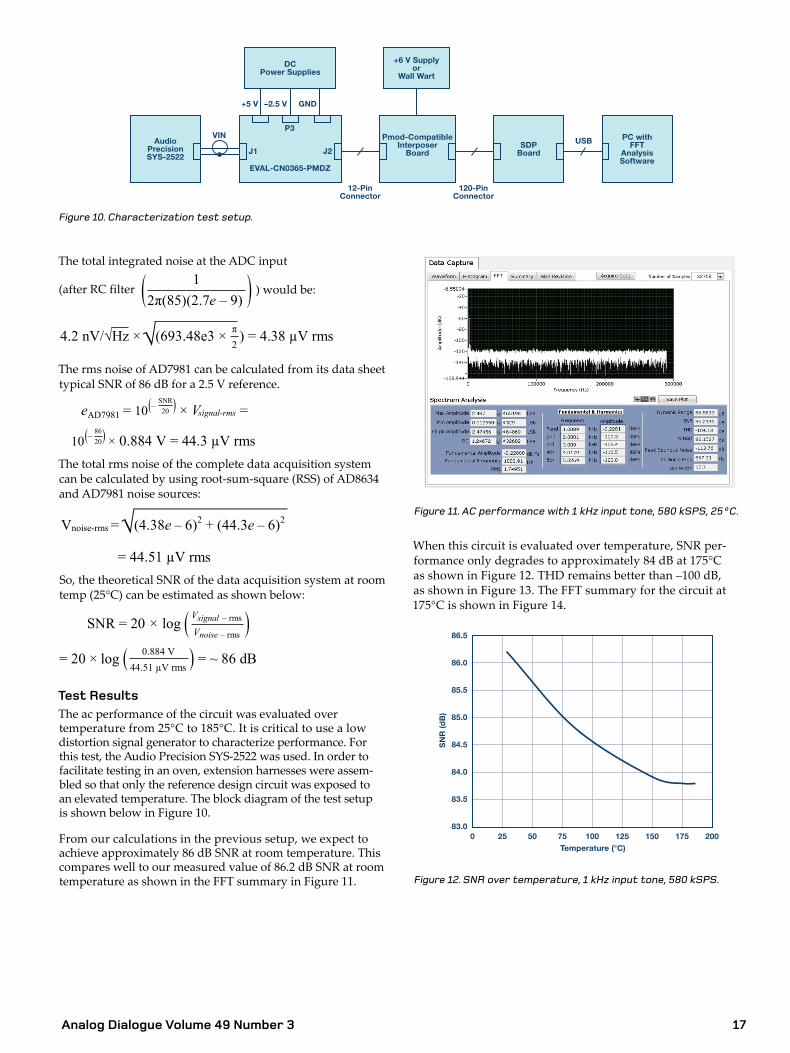
The ac performance of the circuit was evaluated over temperature from 25degC to 185degC It is critical to use a low distortion signal generator to characterize performance For this test the Audio Precision SYS-2522 was used In order to facilitate testing in an oven extension harnesses were assem-bled so that only the reference design circuit was exposed to an elevated temperature The block diagram of the test setup is shown below in Figure 10
From our calculations in the previous setup we expect to achieve approximately 86 dB SNR at room temperature This compares well to our measured value of 862 dB SNR at room temperature as shown in the FFT summary in Figure 11
AudioPrecisionSYS-2522
J1 J2
EVAL-CN0365-PMDZ
DCPower Supplies
P3Pmod-Compatible
InterposerBoard
12-PinConnector
120-PinConnector
SDPBoard
PC withFFT
AnalysisSoftware
ndash25 V+5 V GND
USB
+6 V Supplyor
Wall Wart
VIN
Figure 10 Characterization test setup
Analog Dialogue Volume 49 Number 318
For more information on this reference design please visit analogcomCN0365 For more information on ADIrsquos high temperature portfolio please visit analogcomhightemp
References
Arkin Michael Jeff Watson Michael Siu and Michael Cusack ldquoPrecision Analog Signal Conditioning Semicondcutors for Operation in Very High Temperature Environmentsrdquo Proceed-ing from the High Temperature Electronics Network 2013
AD7981
Digilent Pmod Interface Specification
Harman George Wire Bonding in Microelectronics McGraw Hill Feb 2010
Phillips Reggie et al ldquoHigh Temperature Ceramic Capacitors for Deep Well Applicationsrdquo CARTS International 2013 Pro-ceedings March 2013
Siewert Thomas Juan Carlos Madeni and Stephen Liu ldquoFor-mation and Growth of Intermetallics at the Interface Between Lead-Free Solders and Copper Substratesrdquo Proceedings of the APEX Conference on Electronics Manufacturing Anaheim California April 2003
Walsh Alan ldquoFront-End Amplifier and RC Filter Design for a Precision SAR Analog-to-Digital Converterrdquo Analog Dialogue Volume 46 Number 4 2012
Walsh Alan ldquoVoltage Reference Design for Precision Suc-cessive-Approximation ADCsrdquo Analog Dialogue Volume 47 Number 2 2013
Watson Jeff and Gustavo Castro ldquoHigh Temperature Electron-ics Pose Design and Reliability Challengesrdquo Analog Dialogue Volume 46 Number 2 2012
Zedniacuteček Tomas Zdeněk Sita and Slavomir Pala ldquoTantalum Capacitor Technology for Extended Operating Temperature Rangerdquo
ndash105
ndash104
ndash103
ndash102
ndash101
ndash100
ndash99
ndash98
0 25 50 75 100 125 150 175 200
TH
D (d
B)
Temperature (degC)
Figure 13 THD over temperature 1 kHz input tone 580 kSPS
Figure 14 AC performance with 1 kHz input tone 580 kSPS 175degC
Summary
In this article we presented a new reference design for high tem-perature data acquisition characterized from room temperature to 175degC This circuit is a complete low power (lt20 mW) data acquisition circuit building block that will take an analog sensor input condition it and digitize it to an SPI serial data stream This reference design is available off the shelf to facilitate testing by designers and includes all schematics bill of materials PCB artwork test software and documentation
Jeff Watson [ jeffreywatsonanalogcom] is a systems applications engineer in the Instrumentation Aerospace and Defense business unit at Analog Devices focusing on high temperature applications Prior to joining ADI he was a design engineer in the downhole oil and gas instrumentation industry and off-highway automotive instrumentationcontrols industry Jeff received his bachelorrsquos and masterrsquos degrees in electrical engineering from Penn State University
Jeff Watson
Maithil Pachchigar [maithilpachchigaranalogcom] is an applications engineer in in the Instrumentation Aerospace and Defense business unit at Analog Devices in Wilmington MA He joined ADI in 2010 and focuses on the precision ADC product portfolio and customers in the instrumentation industrial healthcare and energy segments Having worked in the semicon-ductor industry since 2005 he has published numerous technical articles He received an MSEE degree from San Jose State University in 2006 and an MBA degree from Silicon Valley University in 2010
Maithil Pachchigar
Also by this Author
High Temperature Electronics Pose Design and Reliability Challenges
Volume 46 Number 2
Also by this Author
RF-to-Bits Solution Offers Precise Phase and Magnitude Data for Material Analysis
Volume 48 Number 4
Analog Dialogue Volume 49 Number 3 19
Also by this Author
High Temperature Electronics Pose Design and Reliability Challenges
Volume 46 Number 2
Also by this Author
RF-to-Bits Solution Offers Precise Phase and Magnitude Data for Material Analysis
Volume 48 Number 4
Analyzing Optimizing and Eliminating Integer Boundary Spurs in Phase-Locked Loops with VCOs at up to 136 GHz By Robert Brennan
A phase-locked loop (PLL) and voltage controlled oscillator (VCO) outputs an RF signal at a certain frequency and ideally this signal would be the only signal present at the output In reality there are unwanted spurious signals and phase noise at the output This article discusses the simulation and elimination of one of the more troublesome spurious signalsmdashinteger boundary spurs
PLL and VCO combinations (PLLVCOs) that are only capa-ble of operating at integer multiples of the phase frequency detector reference frequency are known as integer-N PLLs PLLVCOs capable of much finer frequency steps are known as fractional-N PLLs Fractional-N PLLVCOs offer much more flexibility and are more widely used Fractional-N PLLs achieve this feat by modulating the feedback path in the PLL at the reference rate While capable of much finer frequency steps than the phase detector reference frequency fractional-N PLLVCOs have spurious outputs called integer boundary spurs (IBS) Integer boundary spurs occur at integer (1 2 3 hellip 20 21 hellip) multiples of the PLLrsquos phase frequency detectorrsquos reference (or comparison) frequency (fPFD) For example if fPFD = 100 MHz there will be integer boundary spurs at 100 MHz 200 MHz 300 MHz hellip 2000 MHz 2100 MHz In a system where the desired VCO output signal is 2001 MHz then there will be an IBS at 2000 MHzmdashthis will appear at a 1 MHz offset from the desired signal Due to effective sampling in the PLL system this 1 MHz offset IBS is aliased to both sides of the desired signal Therefore when the desired output is 2001 MHz spurious signals will be present at 2000 MHz and 2002 MHz
Integer boundary spurs are undesirable for two main reasonsbull If they are at low frequency offsets from the carrier (the
desired signal) then the IBS power contributes to integrated phase noise
bull If they are at large frequency offsets from the carrier then the IBS will modulatedemodulate adjacent channels to the desired channel and result in distortion in system
In some systems high integer boundary spurs render some output channels unusable If a system has 1000 channels in a certain spectrum bandwidth and 10 of the channels have spurious signals above a certain power level those 100 channels may be unusable In protocols where spectrum bandwidth costs a lot of money it is wasteful if 10 of the available channels cannot be used
Integer boundary spurs are strongest when the integer bound-ary falls within the PLL bandwidth from the desired output frequency That is if the output frequency is 200001 MHz and the loop bandwidth is 50 kHz the IBS will be strongest As the output frequency moves away from the integer boundary the power of the IBS reduces in a calculable and repeatable manner Analog Devicesrsquo new free simulatormdash ADIsimFrequencyPlannertrademdashuses this predictable behavior to accurately simulate integer boundary spur power (and much more)
Figure 1 shows the worst-case integer boundary spur power at each output frequency from 1900 MHz to 2150 MHz (1 MHz steps) It can be seen that at 2001 MHz the worst- case IBS power is ndash70 dBc (70 dB below the carrier power) At 2000 MHz there is no IBS because the output frequency falls on an integer boundary The IBS power reduces as the carrier moves away from the integer boundary until the carrier starts getting close to the next integer boundary
The spurious signals seen halfway between the integer bound-aries (2049 MHz and 2051 MHz in Figure 1) are second-order integer boundary spurs Second-order integer boundary spurs occur halfway between integer boundaries Typically second-order IBS are 10 dB to 20 dB lower than first-order IBS ADIsimFrequencyPlanner simulates first- second- third- fourth- and fifth-order integer boundary spurs
ndash25
ndash15
ndash5
ndash35
ndash55
ndash45
ndash65
ndash85
ndash75
ndash95
ndash115
ndash105
ndash1251900 1950 2000 2050 2100 2150
Wo
rst-
Cas
e S
pur
Po
wer
(dB
c)
Output Frequency (MHz)
Spur Power (dBc)
Figure 1 Worst-case integer boundary spur power at each output frequency from 1900 MHz to 2150 MHz (1 MHz steps 100 kHz loop bandwidth HMC830)
Suppose a certain modulation scheme states that channels with integer boundary spur power above ndash80 dBc are unus-able then about 10 of the channels in Figure 1 are no longer available To overcome this problem ADIsimFrequencyPlan-ner can optimize the PLLVCO configuration to reduce and in most cases eliminate integer boundary spurs Recall that the integer boundary spurs occur at integer multiples of the PFD frequency and that they are strongest when near the carrier frequency If the PFD frequency can be changed so that the integer multiple of the PFD frequency falls at a large enough offset from the carrier frequency then the IBS power will be reduced to a nonproblematic level This is what the algorithm in ADIsimFrequencyPlanner doesmdashwhile taking into account the relative powers of the first- through fifth-order integer boundary spurs ADIsimFrequencyPlanner finds the optimum solution that results in the lowest possible integer boundary spurs at the VCO output
How can the PFD frequency be changed Traditionally in a PLLVCO system the PFD frequency is kept fixed However
Analog Dialogue Volume 49 Number 320
the end applicationrsquos firmware can read and then program the HMC7044 and the PLLVCO accordingly ADIsimFrequency-Planner also generates a series of plots to show the user what is happening
In Figure 3 the user has used the same configuration as Figure 1 except this time the PFD frequency is optimized by changing the HMC7044 output divider and the PLL reference input divider The unoptimized simulation is also shown in gray for comparison
ndash25
ndash15
ndash5
ndash35
ndash55
ndash45
ndash65
ndash85
ndash75
ndash95
ndash115
ndash105
ndash1251900 1950 2000 2050 2100 2150
Wo
rst
Cas
e S
pur
Po
wer
(dB
c)
Output Frequency (MHz)
Spur Power (Fixed PFD Frequency 100 MHz)
Spur Power (dBc) (Optimized)
Figure 3 Same output configuration as Figure 1 but now the PFD frequency is optimized
It can be seen in Figure 3 that across the output range (1900 MHz to 2150 MHz in 1 MHz steps) all integer boundary spurs are now lt ndash95 dBc This represents a dramatic improvement and makes a very high percentage of the desired outputs all the same excellent quality
Applying ADIsimFrequencyPlanner to a Wideband VCO
In an experiment to measure the accuracy and effectiveness of ADIsimFrequencyPlanner several of Analog Devices high performance parts were put together and evaluated in the lab-oratory In the experiment the following parts were used
bull HMC7044 clock generation and distributionbull Up to 32 GHz outputbull JESD204B compatiblebull Ultralow noise (lt50 fs jitter 12 kHz to 20 MHz)bull ndash142 dBcHz at 800 kHz offset from 98304 MHz outputbull 16 programmable outputs
bull ADF5355 integrated PLL and VCObull 55 MHz to 136 GHz outputbull 5 mm times 5 mm LFCSP packagebull ndash138 dBcHz at 1 MHz offset from a 34 GHz output
bull HMC704 ultralow noise PLLbull RF input up to 8 GHzbull 100 MHz maximum PFD frequencybull ndash233 dBcHz normalized phase noise floor
Although the ADF5355 has an internal PLL the HMC704 was used to externally lock the ADF5355 VCO There are two main benefits to this technique1 The overall phase noise benefits from the industry-
leading VCO phase noise of the ADF5355 and from the industry-leading PLL phase noise of the HMC704
2 Isolating the VCO and PLL results in less unwanted signal coupling and therefore reduces the power of spurious signals
by making the most of a programmable clock distribution source the PLL reference input divider and the PLL fractional-N modulator architecture it is now easy to change the PFD fre-quency for each output channel
In the recommended solution the new HMC7044 clock gen-eration and distribution chip is used The HMC7044 has 14 ultralow noise outputs each of the 14 outputs has a program-mable divider By connecting one of these outputs to the PLL reference input and then programming the output divider as needed an array of reference frequencies becomes available to the PLL
The HMC7044 is a clock distribution system applicable to applications that use numerous synchronized clocks for ADCs DACs and other system components Simpler applications that donrsquot require as many outputs can use a simpler alterna-tive such as the HMC832 or ADF4351mdashboth are integrated PLL and VCO chips
Then at the PLL reference input the reference input divider (R divider) can be programmed as needed to divide the array of available reference frequencies to a larger array of PFD fre-quencies (the PFD frequency is the frequency at the output of the R divider) Thanks to the high order fractional-N modula-tor in the PLL a change to the PFD frequency does not cause a problem in achieving the desired output frequency Also the programmable charge pump current of the PLL can be used to compensate for any change in the PFD frequency and there-fore maintain a constant-loop bandwidth
ReferenceOscillator
TCXOVCXO
PLLVCOTunableReferenceHMC7044HMC832ADF4351
Selection ofReference
Frequencies
Selectionof PFD
Frequencies
ProgrammableR Divider PFD
divide N
Figure 2 Block diagram showing a selection of PFD frequencies
Example
fPFD (MHz) N ICP fPFD times N = RFOUT (MHz) Comments
100 2001 208 2001 IBS at plusmn1 MHz
75 2668 188 2001 IBS at plusmn24 MHz
where ICP = programmable charge pump current fPFD = PLL PFD frequency N = PLL fractional-N value RFOUT = VCO output frequencycarrier frequency desired signal
The programmable charge pump current changes inversely with the PFD frequencymdashas PFD frequency increases the charge pump current must decrease This serves to keep the loop filter dynamic constant
When using ADIsimFrequencyPlanner the user inputs the required output frequency range step size PFD frequency and reference frequency constraints and loop filter parame-ters The user also selects the available clock generator output dividers and PLL reference input dividers ADIsimFrequency-Planner then steps through each desired frequency step and calculates the optimum PFD frequency from the array of avail-able PFD frequencies ADIsimFrequencyPlanner then returns the required divider settings and charge pump current to the user The data can be easily exported to a lookup table that
Analog Dialogue Volume 49 Number 3 21
ADIsimFrequencyPlanner was used to optimize an output range from 4800 MHz to 6300 MHz in 250 kHz steps (6000 steps) At each step the optimum divider settings (therefore optimum PFD frequency) and charge pump current was pro-grammed to the HMC7044 ADF5355 and HMC704 Once the parts were programmed to an output step a spectrum analyzer measured the carrier power and power of the first- order and second-order integer boundary spurs The spectrum analyzer used a very narrow frequency span and resolution bandwidthmdasheven so at most channels only noise was mea-sured because the integer boundary spur power was lower than the instrumentrsquos noise floor
The following measurement was taken with the PFD frequency constrained between 60 MHz and 100 MHz The loop band-width and phase margin were 17 kHz and 496deg respectively
Figure 4 shows the measured and simulated results for the HMC7044 ADF5355 and HMC704 solutionbull 6000 output channels were simulated and measuredbull Most integer boundary spurs are simulated around ndash120 dBc
This is below the noise floor of the spectrum analyzer so only noise was measured
bull Most frequencies have spurs below ndash100 dBc A typical requirement is ndash70 dBc to ndash80 dBc
bull The only region where the optimization doesnrsquot improve the IBS is less than 2 MHz wide and occurs at 2 times HMC7044 master clockmdashat this frequency no combination of dividers can improve the IBS performance Alternative solutions are offered below
ndash40
ndash20
0
ndash60
ndash80
ndash100
ndash120
ndash1404800 5100 5400 5700 6000 6300
Sp
ur P
ow
er (d
Bc)
Output Frequency (MHz)
Measured (Worst of First- and Second-Order IBS)
Simulated (Optimized PFD Frequency)
Simulated (Fixed PFD Frequency)
Figure 4 Measured and simulated results for the HMC7044 ADF5355 and HMC704 Note the narrow frequency range where optimization was not possible is correctly simulated by ADIsimFrequencyPlanner At most other frequencies the measure-ment was limited by the noise floor of the spectrum analyzer
There is only one very narrow range of frequencies where optimizing the PFD frequency does not improve the IBS per-formance This frequency range is twice the system master clock (in this case 294912 MHz times 2 = 589824 MHz) At this frequency if the application is capable it is recommended to shift the carrier frequency to a nearby cleaner frequency and then shift the baseband frequency in digital (NCO) to com-pensate For example offset the carrier frequency 2 MHz and offset the digital baseband frequency 2 MHz to compensate Alternatively if possible in the system change the master clock frequency to create a clean output frequency
If the simpler solution mentioned above (using the HMC832 or ADF4351 instead of the HMC7044) then no problem fre-quencies exist
From Figure 4 it can be seen that ADIsimFrequencyPlannerbull Simulates integer boundary spurs accuratelybull Successfully optimizes the reference source and PLLVCO
system for excellent integer boundary spur performance bull This makes more channels in a range usable and
therefore increases value for money in expensive frequency spectrums
bull Simulates wide frequency range systems very quickly Manually the process can take days or even weeks The above 6000 step simulation takes less than one minute in ADIsimFrequencyPlanner
Resources
ADF5355
ADIsimFrequency Planner
HMC704
HMC7044
Acknowledgments
Mark Cloutier staff scientist of the RF and Microwave Group for Analog Devices Don Young applications manager in the RF and Microwave Group for Analog Devices
Robert Brennan [robertbrennananalogcom] joined Analog Devices in 2010 after graduating with a bachelorrsquos in electronic engineering from University of Limerick Ireland He worked at the Analog Devices Limerick office for several years before relocating to the US He is currently a senior applications engineer in the RF and Microwave Group based in Massachusetts His primary focus is on PLLs VCOs and integrated PLLVCOs Follow Robert on Analog Devices EngineerZone community at httpsezanalogcompeoplerbrennan
Robert Brennan
Analog Dialogue Volume 49 Number 322
Interleaving ADCs Unraveling the Mysteries By Gabriele Manganaro and Dave Robertson
Time interleaving is a technique that allows the use of multiple identical analog-to-digital converters1 (ADCs) to process regular sample data series at a faster rate than the operating sample rate of each individual data converter In very simple terms time interleaving (IL) consists of time multiplexing a parallel array of M identical ADCs as shown in Figure 1 to achieve a higher net sample rate fs (with sam-pling period Ts = 1fs) even though each ADC in the array is actually sampling (and converting) at the lower rate of fsM So for example by interleaving four 10-bit100 MSPS ADCs one could in principle realize a 10-bit400 MSPS ADC
To better understand the principle of IL in Figure 1 an analog input VIN(t) is sampled by the M ADCs and results in a com-bined digital output data series DOUT ADC1 will sample VIN(t0) first and begin converting it into an n-bit digital representa-tion Ts seconds later ADC2 will sample VIN(t0 + Ts) and begin converting it into an n-bit digital representation Then Ts seconds later ADC3 will sample VIN(t0 + 2Ts) and so on After ADCM has sampled VIN(t0 + (M-1) times Ts) the next sampling cycle starts with ADC1 sampling VIN(t0 + M times Ts) and this car-ousel carries on
As the n-bit outputs of the ADCs become sequentially available in the same order as just described for the sam- pling operation these digital n-bit words are collected by the demultiplexer shown on the right hand side of the same figure Here the recombined data out sequence DOUT(t0 + L) DOUT(t0 + L + Ts) DOUT(t0 + L + 2Ts) is obtained L stands for the fixed conversion time of each individual ADC and this recombined data sequence is an n-bit data series with sample rate fs So while the individual ADCs often referred to as the
ldquochannelsrdquo are n-bit ADCs sampling at fsM the ensemble con-tained in the box is equivalent to a single n-bit ADC sampling at fs and we will refer to that as the time interleaved ADC (distin-guishing it from the channels) Basically the input is sliced and separately processed by the ADCs in the array and then consistently reassembled at the output to form the high data rate representation DOUT of the input VIN
This powerful technique is not free of practical challenges The key issue manifests itself when the M data streams coming from the channels are digitally assembled together to recon-struct the original input signal VIN If we look at the spectrum of DOUT in addition to seeing the digital representation of VIN and the distortion introduced by the analog-to-digital con-version we will also see additional and substantial spurious content termed ldquointerleaving spursrdquo (or IL spurs in short) IL spurs neither have the signature of polynomial type dis-tortions like higher order signal harmonics (2nd 3rd and so on) nor the signature of quantization or DNL errors IL arti-facts can be seen as a form of time-domain fixed pattern noise and are introduced by analog impairments in the channels that due to the interleaving process modulate with the sliced converted signals and ultimately show up in the final digitized output DOUT
Letrsquos begin understanding what might be happening by analyzing a simple example Consider the case of a two-way interleaved ADC with a sinusoidal input VIN at frequency fIN Assume that ADC1 has a gain G1 and that ADC2 has a differ-ent gain G2 In such a two-way IL ADC the ADC1 and ADC2 will alternate in sampling VIN So if ADC1 converts the even samples and ADC2 converts the odd samples then all the even data of DOUT has an amplitude set by G1 while all the odd data of DOUT has an amplitude set by G2 Then DOUT doesnrsquot only contain VIN along with some polynomial distortion but it has been subject to the alternate magnification of G1 and G2 just as if we were instead amplitude modulating VIN with a square wave at frequency fs2 That is what will introduce additional spurious content Specifically DOUT will include a ldquogain spurrdquo at frequency fs2 ndash fIN and unfortunately this spurrsquos frequency tracks the input fIN and it is located within the first Nyquist band of the interleaved ADC (that is within fs2) and there are also aliases of it on all other Nyquist bands The powermag-nitude of this interleaving spur depends on the net difference between the two gains G1 and G2 In other words it depends on the gain error mismatch2 And finally it depends on the magnitude of the input VIN itself
fs
fsM
fsM
fsM
fsM
ADC1
ADC2
ADC3
ADC4
fs
VIN DOUT
fsM
fsM
fsM
n
n
n
n
ADC1
ADC2
ADCM
fs
fsM
fsM
fsM
fsM
ADC1
ADC2
ADC3
ADC4
fs
VIN DOUT
fsM
fsM
fsM
n
n
n
n
ADC1
ADC2
ADCM
Figure 1 An array of M time interleaved n-bit ADCs The sample rate of each one is fsM the resulting sample rate of the time interleaved ADCs is fs An example of clocking scheme for the case of M = 4 is depicted on the lower part of this figure
1 While analog-to-digital converters are discussed here all the same principles are applicable to the time interleaving of digital-to-analog converters
2 Note that it is the gain error mismatch that matters not its absolute value Because if both channels have the same gain (error) then G1 = G2 In that case the two channels are equally scaled up so the two data streams are recombined into a single DOUT data stream without alternating amplitude (or modulation) and no gain spur is introduced
Analog Dialogue Volume 49 Number 3 23
clocked at fs2 though we are still consuming at least twice the power of such a single channel The interleaving spu-rious image on the upper end of the Nyquist band can be suppressed by digital filtering after digitization and does not require correcting for analog impairments
The good news however is that since the ping pong ADC is clocked at fs the digitized output benefits from a 3 dB pro-cessing gain in dynamic range Moreover compared to using a single ADC clocked at fs2 the antialiasing filter design has been relaxed for the ping pong ADC
fs
VIN DOUT
fs2
fs2
n
n
n
ADC1
ADC2
(a)
fIN INf
f
ff
s2
fs4fs4
fs2
fINfs2 ndash fINfs2 ndash
1st Nyquist
(b)
(c)
DIN(f) DIN(f)
Interleaving Spurs Interleaving Spurs
Input Signal
Input Signal
Figure 2 (a) A ping pong scheme (b) the output spectrum when a narrow-band input signal lies below fs4 and (c) when the input signal lies between fs4 and the Nyquist frequency fs2
All the same considerations can be repeated if the narrow-band signal is located on the upper half of the first Nyquist band as shown in Figure 2(c) since the interleaving image spur is moved to the lower half of the Nyquist band Once again the gain and timing spur can be digitally suppressed after digiti-zation by filtering
Finally the input signal and the interleaving spurs will fre-quency overlap and the input spectrum gets corrupted by the interleaving image as soon as the input signal frequency location crosses the fs4 line In this case recovering the desired input signal is not possible and the ping pong scheme is not usable Unless of course the channel-to-channel matching is sufficiently close to make the interleaving spurious content acceptably low for the application or if calibration is employed to reduce the causes leading to IL images
In summary frequency planning and some digital filtering allow recovering the narrow-band digitized input in a ping pong scheme even in the presence of channel mismatch While the converter power consumption roughly doubles compared to the case of using a single ADC clocked at fs2 the ping pong scheme provides a 3 dB processing gain and relaxes antialiasing requirements
An example of a ping pong without any correction for chan-nel mismatch and its resulting interleaving spurs is shown in
If the input isnrsquot a simple sine wave but as in a real applica-tion case it is a whole band limited signal then the ldquogain spurrdquo isnrsquot simply an undesired tone it is instead a complete scaled image of the band limited input signal itself that shows up within the Nyquist band This to some extent negates the ben-efits of the increased bandwidth provided by interleaving
While in the above example we have considered only the gain error mismatch between the channels other impairments introduce interleaving spurs too Offset mismatch (differ-ence between the channelsrsquo offsets) introduces tones (ldquooffset spursrdquo) at fixed frequency and with power proportional to the offset mismatch3 Sampling time skew occurs when some of the channels sample a bit earlier or later than they should in the intended order That introduces ldquotiming spursrdquo that lie at the very same frequency (and add up to the same amplitude) as the gain spurs4 but with power that is increasingly stronger as fIN grows and as the input amplitude grows Bandwidth mis-match between the individual channels introduces yet more spurious content at frequencies that depend on fIN and just like the timing spurs the spurious power gets progressively stronger with fIN itself not just with the input amplitude Again in all cases the severity of the spectral degradation of the output isnrsquot dependent on the absolute value of the channelsrsquo impairments (offset gain timing band) but on the relative mismatchesdifferences between them
While the general technique of time interleaving has been around for several decades the degree with which the IL spurs could be kept minimal has limited its past applicability to low resolution converters However recent advances in the calibration of channel mismatch and in the suppression of the residual IL spurious content is allowing today the realization of fully integrated very high speed 12- 14- and 16-bit IL ADCs
At this point we need to distinguish between some classes of interleaving We generally refer to ldquoping pongrdquo operation in the case of two interleaved channels We can then distinguish between ldquolightly interleavedrdquo and ldquohighly interleavedrdquo as we refer to the cases of a reduced number of channelsmdashfor exam-ple three channels to four channelsmdashor the case of a large number of channels say more than four and often eight of more respectively
Ping Pong (Two-Way) Interleaving
When we interleave only two channels to double the net sample rate as shown in the block diagram of Figure 2(a) we term that ldquoping pongrdquo This is an especially simple case that has some interesting and useful features In this case within the 1st Nyquist band of the interleaved ADC the interleaving spurs are located at dc at fs2 and at fs2 ndash fIN So if the input signal VIN is a narrow-band signal centered at fIN as depicted in the first Nyquist output spectra of Figure 2(b) the interleav-ing spurs will consist of an offset spur at dc another offset mismatch spur at fs2 and a gain and timing spurious image centered at fs2 ndash fIN that looks like a scaled copy of the input itself
If the input signal VIN(f) is completely bound between 0 and fs4 as in Figure 2(b) then the interleaving spurs are not fre-quency overlapping with the digitized input In this case the bad news is that we are only able to digitize in half of the Nyquist band namely just like if we had a single channel
3 In general for M channel interleaving the offset spurs occur at fOS = (kM) fS for k = 012 (Manganaro 2011)
4 In general for M channel interleaving the gain and the timing skew images occur at fGS = plusmn fIN + (kM) fS with k = 12 (Manganaro 2011)
Analog Dialogue Volume 49 Number 324
Figure 3 In this case the two ADCs of the dual 14-bit1 GSPS ADC AD9680 sample at alternate times a single sine wave hence returning a single combined output data stream at 2 GSPS When we look at the 1st Nyquist band of the output spectrum of this ping pong schememdashthat is between dc and 1 GHzmdashwe can see the input tone which is the strong tone on the left at fIN = 400 MHz we can also see the strong gaintiming mismatch spur at fs2 ndash fIN = 2G2 ndash 400 M = 600 MHz We also see a number of other tones due to the two channelsrsquo own distortion as well as other impairments but these are all below the ndash90 dB line
0
ndash15
ndash30
ndash45
ndash60
ndash75
ndash90
ndash105
ndash120
ndash135
95
5
190 285 380 475 570 665 760 855 950
dB
Frequency (MHz)
46 3
+
2
Figure 3 Spectrum of the combined 2GSPS output data of a ping pong scheme obtained by clocking the two ADCs of the AD9680 with a 1 GSPS clock but with 180o sampling phase shift
Higher Order Interleaving
When we have more than two channels frequency planning as described above is not very practical or attractive The location of the interleaving spurs cannot be confined to a frac-tion of the Nyquist band For example consider the case of a four-way interleaved ADC as shown in Figure 4(a) In this case the offset mismatches give rise to tones at dc fs4 and fs2 While the gain and timing interleaving images are located at fs4 ndash fIN fs4 + fIN and fs2 ndash fIN An example of the spectrum of the interleaved ADCrsquos output is shown in Figure 4(b) It can be clearly seen that unless the input is within a bandwidth of less than fs8 no matter where we place fIN the input will over-lap with some of the interleaving spurs and if the input is a very narrow-band signal we shouldnrsquot try to digitize it with a wideband interleaved ADC
In a case like this we need to minimize the IL spurious power to obtain full Nyquist and a cleaner spectrum In order to do that calibration techniques are used to compensate for the mismatch between the channels As the effect of the mismatches is corrected the power of the resulting IL spurs decreases Both the SFDR and the SNR benefit from the reduction of this spurious power
Compensation approaches are limited by the accuracy with which the mismatches can be measured and ultimately cor-rected To further suppress the residual spurs beyond the level achieved via calibration it is possible to intermittently and randomly shuffle the order with which the channels sample the input In doing so the previously discussed modulation effects of the converted input signal due to the uncalibrated mismatches turn from a fixed pattern noise to pseudorandom As a result IL tones and undesired periodic patterns turn into pseudorandom noise-like content that adds with the con-verter quantization noise floor and leads to the disappearance
or at least to spreading of the undesired spurious images and tones In this case the power associated with the IL spurious content adds to the power of the noise floor Hence while distortion improves SNR can degrade by the amount of IL spurious power added to the noise SNDR (SINAD) is essen-tially unchanged as it combines both distortion and noise and randomization it simply moves the IL contribution from a component (distortion) to the other (noise)
fs
VIN DOUT
(a)
fIN
f
fs2
(b)
DIN(f)
Input Signal
fs4
fs4
fs4
fs4
ADC1
ADC2
ADC3
ADC4n
n
n
n
n
fs4
Interleaving Spurs
Figure 4 (a) A four-way interleaved ADC and (b) the correspond-ing 1st Nyquist output spectrum showing the interleaving spurs
Let us consider some examples of interleaved ADCs The AD9625 is a 12-bit25 GSPS three-way interleaved ADC The mismatches between the three channels are calibrated in order to minimize the interleaving spurs An example of its output spectrum with an input close to 1 GHz is depicted in Figure 5(a) In this spectrum besides the ~1 GHz input tone it is possible to see the channelsrsquo 2nd and 3rd harmonic distortion near 500 MHz and the 4th harmonic distortion near the funda-mental The interleaving mismatch calibration substantially minimizes the power of the interleaving spurs and a large set of additional residual small spurious tones is visible across the entire spectrum
In order to further reduce such residual spurious content channel randomization is introduced A fourth calibrated channel is added and the four channels are then three-way interleaved in randomly changing order by intermittently swapping one of the interleaved channels with the fourth one One can liken that to a juggler playing with three Skittles up in the air while a fourth one is swapped in every so often By doing so the residual interleaving spurious power is randomized and spread out over the noise floor As shown in Figure 5(b) after channel randomization the interleaving spurs have nearly disappeared while the power of the noise has marginally increased hence degrading the SNR by 2 dB Note of course that while the second spectrum shown in Figure 5(b) is considerably cleaner of distortion tones the shuffling cannot affect the 2nd 3rd and 4th harmonic since these arenrsquot interleaving spurs
Analog Dialogue Volume 49 Number 3 25
0
ndash15
ndash30
ndash45
ndash60
ndash75
ndash90
ndash105
ndash120
ndash135
150 300 450 600 750 900 1050 1200
5
dB
Frequency (MHz)
ILS2+ILS4ndash ILS4+2
34
6
+
fs4
(a)
0
ndash15
ndash30
ndash45
ndash60
ndash75
ndash90
ndash105
ndash120
ndash135
150 300 450 600 750 900 1050 1200
5
dB
Frequency (MHz)
ILS2+ILS4ndash ILS4+
2
34
6fs4+
(b)
Figure 5 The output spectrum of the AD9625 clocked at 25 GSPS and with an input tone close to 1 GHz (a) Sequential three-way interleaving SNR = 60 dBFS the SFDR = 72 dBc is limited by the third harmonic near 500 MHz however a number of interleaving spurs are visible all across the spectrum (b) Three-way inter-leaving with random channel shuffling SNR = 58 dBFS while the SFDR = 72 dBc is still set by the third harmonic all the interleav-ing spurs have been eliminated by spreading their power over the noise floor
Another example of an interleaved ADC using channel ran-domization is the one shown in the spectra of Figure 6 This is the case of the four-way interleaved 16-bit310 MSPS ADC AD9652 In the case shown in Figure 6 the four channels are sequentially interleaved in a fixed sequence while no effort is made to calibrate them to reduce channel mismatch The spectrum shows clearly the interleaving spurs at the predicted frequency locations and their large power is far greater than the 2nd and 3rd harmonics and limits the spurious-free dynamic range to only 57 dBc
However if the same ADC is foreground calibrated to reduce the channel mismatch the power of the interleaving spurs is substantially reduced as shown in Figure 7 Similar to the case of the previous example the channel harmonic distor-tion isnrsquot affected however the interleaving spurs are greatly reduced in power through channel mismatch calibration
Lastly the spectral purity in Figure 7 can be further improved by randomizing the channel order as shown in Figure 8 In this case the randomization uses a proprietary technique that while intermittently scrambling the order of the four channels doesnrsquot require a spare (5th) channel to be added hence saving its associated power It can be seen in Figure 8 that after ran-domization only regular harmonic distortion is left on the resulting spectrum
0
ndash20
ndash40
ndash60
ndash80
ndash100
ndash120
ndash1400
HD3 HD2
50 100 150
dB
Frequency (MHz)
GS4+GS4ndash
IL Spurs
OS2OS4
GS2
OS2 = fs2 Offset SpurOS4 = fs4 Offset SpurGS2 = fs2 plusmn fIN SpurGS4plusmn = fs4 plusmn fIN Spurs
SFDR = 57 dBSNR = 55 dB
Figure 6 The output spectrum of the AD9652 clocked at fs = 310 MHz and with a sinusoidal input at fIN ~ 70 MHz In this case no channel calibration and randomization is applied The 2nd (HD2) and aliased 3rd (HD3) harmonics are visible at ~140 MHz and ~100 MHz respectively Interleaving (IL) spurs are visible as well These are the offset tones at dc fs2 (OS2 in the graph) and fs4 (OS4 in the graph) Moreover the gain (timing) spurs can be found at fs2 - fIN (GS2 in the graph) fs4 + fIN (GS4+ in the graph) and fs4 - fIN (GS4- in the graph) The SNR quote in this graph is artificially poor due to the fact that some of the spurious content has been lumped with the noise power
0
ndash20
ndash40
ndash60
ndash80
ndash100
ndash120
ndash1400 50 100 150
dB
Frequency (MHz)
SFDR = 87 dBSNR = 74 dB
HD3HD2IL Spurs Reduced
GS2GS4ndash GS4+OS2
OS4
Figure 7 The output spectrum for the same AD9652 with the same input but after calibrating the four channels to reduce their mismatch Comparing with Figure 6 while the 2nd and 3rd harmonics are unaffected the interleaving spursrsquo power has substantially been reduced and the SFDR has improved by 30 dB going from 57 dBc to 87 dBc
Analog Dialogue Volume 49 Number 326
0
ndash20
ndash40
ndash60
ndash80
ndash100
ndash120
ndash1400 50 100 150
dB
Frequency (MHz)
SFDR = 87 dBSNR = 74 dB
HD3HD2
No IL SpursGS2
GS4ndashGS4+
OS2OS4
Figure 8 The output spectrum for the previous case once the randomization of the interleaving order is turned on Randomizing the residual interleaving spurs distributes their power over the noise floor and the corresponding peaks disappear Only regular harmonic distortion is left in sight The SNR is nearly unaffected as the distributed spurious power from the interleaving tones is rather negligible after the mismatch calibration
Conclusion
Time interleaving is a powerful technique to increase the bandwidth of data converters Recent advances in mismatch compensation as well as cancellation of residual spurious content via randomization techniques have allowed the fully integrated realization of very high speed 12- 14- and 16-bit interleaved ADCs
In the case in which the input signal is band limited such as for example in a number of communication applications a ping pong (two-way) interleaving approach allows allocating the undesired interleaving spurs away from the input band of interest via frequency planning The spurious content can then be digitally filtered While this approach consumes roughly twice the power compared to a noninterleaved ADC at half the IL sample rate required to capture the same spurious-free input bandwidth on the other hand it both increases the dynamic range by 3 dB via processing gain and it also relaxes
the roll-off of the antialiasing and roofing filters that precede the ADC thanks to the higher IL sample rate
When the full input band of the IL converter is required to capture a wideband input signal a higher order interleaving converter is appropriate In this case calibration and random shuffling allow interleaving distortion and spurious content compensation and cancellation
AcknowledgmentsThe authors would like to acknowledge Siddharth Devarajan Prawal Shrestha Antony DeSimone Ahmed Ali Umesh Jayamohan and Scott Bardsley for capturing and providing some of the experimental results
ReferencesBeavers Ian ldquoGigasample ADCs Run Fast to Solve New Challengesrdquo Analog Devices 2014 Black William and David Hodges ldquoTime Interleaved Converter Arraysrdquo IEEE Journal of Solid-State Circuit Vol SC-15 No 6 1980Bosworth Duncan ldquoGSPS Data Converters to the Rescue for Electronics Surveillance and Warfare Systemsrdquo Analog Devices 2014Elbornsson Jonas Fredrik Gustafsson and Jan-Erik Eklund
ldquoAnalysis of Mismatch Effects in a Randomly Interleaved AD Converter Systemrdquo IEEE Transactions on Circuits and Systems Vol 52 No 3 2005Harris Jonathan ldquoFurther into the Alphabet with Interleaved ADCsrdquo EDN Network 2013Harris Jonathan ldquoThe ABCs of Interleaved ADCsrdquo EDN Network 2013Manganaro Gabriele Advanced Data Converters Cambridge UK Cambridge University Press 2011
Gabriele Manganaro [gabrielemanganaroanalogcom] holds a DrEng and a PhD in electronics from the University of Catania Italy Starting in 1994 he did research with ST Microelectronics and at Texas AampM University He worked in data converter IC design at Texas Instruments Engim Inc and as Design Director at National Semiconductor Since 2010 he has been an engineering director for High Speed Converters at Analog Devices He served in the technical subcommittee for Data Converters of the ISSCC for seven consecutive years He was Associate Editor then Deputy Editor in Chief and Finally Editor in Chief for IEEE Transactions on Circuits and SystemsmdashPart I He authoredcoauthored 60 papers three books and holds 13 US patents with more pending He is a Senior Member IEEE (since 2003) and a Fellow of the IET (since 2009)
Gabriele Manganaro
David H Robertson [davidrobertsonanalogcom] has been with the Data Converter group of Analog Devices since 1985 He has worked on a wide variety of high speed digital-to-analog and analog-to-digital converters on complementary bipolar BiCMOS and CMOS processes He has held positions as a product engineer design engineer and product line director working with product development teams in the US Ireland Korea Japan and China Dave is presently the Product and Technology Director for ADIrsquos High Speed Converter group
Dave holds 15 patents on converter and mixed-signal circuits has participated in two ldquobest panelrdquo International Solid-State Circuits Conference evening panel sessions and was coauthor of the paper that received the IEEE Journal of Solid-State Circuits 1997 Best Paper Award He served on the ISSCC technical program committee from 2000 through 2008 chairing the Analog and Data Converter subcommittees from 2002 to 2008
David H Robertson
Analog Dialogue Volume 49 Number 3 27
Zero-Drift Amplifiers Now Easy to Use in High Precision Circuits By Vicky Wong and Yoshinori Kusuda
A zero-drift amplifier as the name suggests is an amplifier with offset voltage drift very close to zero It uses auto-zero or chopping technology or a combination of both to continuously self-correct for dc errors over time and temperature This enables the amplifier to achieve microvolt-level offsets and extremely low offset drifts Therefore it is uniquely suited to be used in signal conditioning circuits with high gain and precision performance For example a sensor (such as a temperature pressure or load cell sensor) typically produces a low level output voltage and hence requires an amplifier to amplify its output without introducing additional errors Zero-drift amplifiers designed for ultralow offset voltage and drift high common-mode rejection high power supply rejection and reduced 1f noise are an ideal choice to achieve a high level of resolution in a demanding system application such as sensing with a long product life cycle
Basic Architecture of a Zero-Drift Amplifier
Figure 1 shows the circuit diagram of a basic chopper amplifier in unity gain configuration The dc gain path consists of an input chopping switch network (CHOPIN) a first transconductance amplifier (Gm1) an output chopping switch network (CHOPOUT) a second transconductance amplifier (Gm2) and frequency compensation capacitors (C1 and C2) CHOP and CHOP are controlled by a clock generator and function to correct unwanted amplifier dc offset voltage (VOS)
Figure 2 shows the associated timing diagram and expected output voltage (VOUT) When the CHOP clock signal is high (A phase) amplifier Gm1rsquos differential input and output are connected to the signal path with no inversion This results in a positive output voltage VOUT due to the presence of VOS When the CHOP clock signal is high (B phase) Gm1rsquos input and output are connected to the signal path with inversion resulting in a negative output voltage due to VOS The positive and negative output voltages from Gm1 result in an output voltage equal to plusmnVOS This chopping concept in the time domain is similar to modulation in the frequency domain In other words the offset voltage of Gm1 is up-modulated by CHOPOUT to the chopping frequency On the other hand the input signal is chopped twice by CHOPIN and CHOPOUT This is equivalent to the input signal being up-modulated and then down-modulated to its original frequency Hence the input signal gets through to the output with no inversion
The positive and negative output voltages (plusmnVOS ) from Gm1 appear as voltage ripples at VOUT (Figure 2) In addition the CHOP and CHOP clocks are coupled to the differential input pins through parasitic capacitances associated with the switches When the clocks change state charges are injected into the differential input pins These charge injections are translated into output voltage glitches via the finite input source impedances The magnitude and shape of the glitches
depend on the amount and matching of the input source impedances and the charge injections at the differential input pins These output ripples and glitches introduce switching artifacts that appear as increases in noise spectrum at the chopping frequency and its multiple integer frequencies Also the magnitude and frequencies of the switching artifacts differ for each zero-drift amplifier and from unit to unit In this article the term chopping and switching frequency are used interchangeably
CHOP CHOP
Gm1 Gm2
C2
VOUT
C1
A
A
A
A
B
B
B
B
CHOP CHOP
VOS
CHOPIN CHOPOUT
VIN
Figure 1 Chopping architecture
AB B B
A A
Clock
VOUT
Time
CHOP
CHOP
Ripples VOS
ndashVOS
Glitches
Figure 2 Chopping timing diagram
Switching Artifacts as Shown on a Data Sheet
Traditionally zero-drift amplifiers have fairly large broadband noise and low switching frequencies ranging from a few kilohertz to a few tens of kilohertz This limits their usage to dc and sub-100 Hz applications so that the switching frequency remains out of the signal bandwidth of interest For applications requiring high precision and low drift at a higher bandwidth it is important to use a zero-drift amplifier with higher switching frequency As a matter of fact the switching frequency is sometimes viewed as the figure of merit for zero-drift amplifiers With advanced design architectures newer zero-drift amplifiers are designed to have smaller switching artifacts at much higher frequencies For example in addition to chopping the offset voltage at 48 MHz the ADA4522-2 a high voltage dual zero-drift amplifier uses a patented offset and ripple correction loop circuity to minimize switching artifacts The correction loop operates at 800 kHz and functions to null out the offset voltage plusmnVOS (as shown in Figure 2) Reducing plusmnVOS to 1 of its original value provides a 40 dB improvement in the switching artifact This reduces the system designerrsquos effort to achieve targeted system level precision
Analog Dialogue Volume 49 Number 328
1 k
100
10
1
011 k 10 k 100 k 1 M 10 M 100 M
Inte
gra
ted
Ou
tpu
t V
olt
age
No
ise
(microV
rm
s)
Frequency (Hz)
ADA4522-2Amplifier AAmplifier B
Figure 5 Integrated output voltage noise
Total rms noise that is integrated at the output of an amplifier depends on the amplifierrsquos bandwidth Output voltage noise rolls off with the available bandwidth therefore the higher the gain or the higher the bandwidth the higher the amplitude of the output amplifier noise Figure 5 shows a graph of integrated output voltage noise vs frequency This is a helpful graph for understanding the total integrated noise with respect to a frequency As an example if the amplifierrsquos bandwidth is limited to 100 kHz by means of filtering the total output noise due to the inherent amplifier voltage noise can be read off the graph and will be as follows
Table 1 Output Integrated Noise
Amplifier Output Noise (microV rms)
Peak-to-Peak Output Noise (microV p-p)
ADA4522-2 191 1261
Amplifier A 333 2198
Amplifier B 640 4224
Using a common multiplier (called crest factor) to convert rms voltage to peak-to-peak voltage a peak-to-peak noise estimation is shown in the third column of Table 1 In a 5 V system the ADA4522-2 would provide 186 bits of peak-to-peak resolution whereas Amplifier B provides 168 bits of peak-to-peak resolution Having a lower total integrated output noise is always desirable as it increases the signal-to-noise ratio and enables a higher resolution to the entire system
Another interesting thing to note about Figure 5 is that the integrated noise increases with a step-like function at the noise spike frequencies The noise spikes (with increased noise energies) albeit narrow add significantly to the total output integrated noise
Switching Artifacts in the Time Domain
Often times the switching artifacts can be clearly seen in the voltage noise density spectrum in the frequency domain To understand the time-based behavior of the switching artifact one can configure the amplifier in a buffer configuration with the noninverting pin grounded and directly monitor
The easiest way to detect the switching artifact is by observing the amplifierrsquos voltage noise density spectrum Figure 3 shows the input referred voltage noise density graph of the ADA4522-2 Note that Channel B exhibits an increase in noise spectrum at its switching frequency of 800 kHz This increase in noise spectrum as described in the earlier part of this article is the byproduct of the charge injection mismatch Since the mismatch is part-to-part and channel-to-channel dependent the magnitude of noise spikes are different and not all units exhibit the noise spike As an example Channel A of the same unit does not exhibit any noise spikes at the switching frequency of 800 kHz The switching frequencies could also differ up to a factor of 10 to 20 from unit to unit due to the on-chip clock oscillator frequency variation
100
10
110 k 100 k 1 M 10 M 100 M
Vo
ltag
e N
ois
e D
ensi
ty (n
Vradic
Hz)
Frequency (Hz)
Channel BChannel A
Figure 3 ADA4522-2 voltage noise density
Noise Comparison Between Different Zero-Drift AmplifiersFigure 4 shows the input referred voltage noise density of three different leading edge high voltage zero-drift amplifiers Note that all three zero-drift amplifiers tested exhibit some sort of switching artifacts Some of the switching artifacts also repeat at its multiple integer frequencies These switching artifacts could be significant and could introduce errors in a circuit design Hence it is important to understand their impact on a circuit and find ways to mitigate the effect If the amplifier has a closed-loop frequency that is higher than the switching frequency this increase in noise spectrum will be integrated across the entire bandwidth and be reflected at the output Not only that this input-referred voltage noise will be gained up by the amplifier noise gain For instance assume that the amplifier is configured in a gain of 100 the effective output referred voltage noise density would also increase by a factor of 100
1 k
100
10
11 k 10 k 100 k 1 M 10 M 100 M
Vo
ltag
e N
ois
e D
ensi
ty (n
Vradic
Hz)
Frequency (Hz)
ADA4522-2Amplifier AAmplifier B
Figure 4 Voltage noise density of different zero-drift amplifiers
Analog Dialogue Volume 49 Number 3 29
the output with an oscilloscope Figure 6 shows the typical output of two zero-drift amplifiers Note that Amplifier A exhibits output voltage spikes in various amplitudes The spikes repeat themselves every 066 μs This matches the noise spikes that are seen at 151 MHz in Figure 4 On the other hand the ADA4522-2 does not exhibit any switching artifact in the time domain (blue graph) In other words the noise spikes that exist are below the noise floor of the measurement system and cannot be detected This allows designers to use the ADA4522-2 in applications such as driving an ADC with confidence that noise spikes will not be an issue
4
2
0
ndash2
ndash4
ndash6
4
2
0
ndash2
ndash4
Vo
ltag
e (m
V)
Vo
ltag
e (m
V)
Time (1 microsDiv)
Amplifier AADA4522-2
Figure 6 Output voltage noise in the time domain
Filters to Mitigate Switching Artifact
RG
RF
RFILTVOUT
CFILT
(a) (b)
RG RF
VOUT
CFILT
Figure 7 Zero-drift amplifier with filter setup
100
10
11 k 10 k 100 k 1 M 10 M 100 M
Vo
ltag
e N
ois
e D
ensi
ty (n
Vradic
Hz)
Frequency (Hz)
AV = +1AV = +1 (Post Filter at 80 kHz)AV = +1 (Post Filter at 8 kHz)
Figure 8 Voltage noise density of a unity-gain zero-drift amplifier with post filter
To reduce the impact of the switching artifacts there are a couple of methods that can be implemented These methods ultimately lead to limiting the amplifier bandwidth such that it is less than the switching frequency Using a filter is an effective way to suppress the noise spikes The easiest design is to place a resistor-capacitor network at the amplifier output to create a low pass filter (Figure 7A) Figure 8 shows the voltage noise density of a zero-drift amplifier with a post filter designed at one or two decades below the switching frequency The noise spike at 800 kHz reduces from 36 nVradicHz (no post filter) to 41 nVradicHz (post filter at 80 kHz)
which is below the amplifierrsquos low frequency broadband noise level With a post filter positioned two decades below the switching frequency (post filter at 8 kHz) the noise spike is no longer visible and the ADA4522-2 looks like any other traditional amplifier
Some applications might not tolerate having an RC network at the output of the amplifier Amplifier output current flowing through the filter resistor creates a voltage offset that introduces output error In this case one can opt to filter the noise spikes by placing a feedback capacitor across the feedback loop (Figure 7(b)) Figure 9 shows the output voltage noise density of an amplifier configured in gain of 10 with no filtering vs having a post filter or a feedback filter positioned a decade below the switching frequency The post filter configuration is more effective as a low-pass filter than the feedback capacitor
100
10
1
0110 k 100 k 1 M 10 M 100 M
Vo
ltag
e N
ois
e D
ensi
ty (n
Vradic
Hz)
Frequency (Hz)
AV = +10AV = +10 with Post Filter at 80 kHzAV = +10 with Feedback Filter at 80 kHz
Figure 9 Switching artifact reduces with filters
Using Zero-Drift Amplifiers in High Gain Configura-tion Helps
A lot of designers have used zero-drift amplifiers but have not observed any switching artifacts in their system One reason could be due to the configuration of the amplifier Zero-drift amplifiers have low drift and offset and are most often used to signal condition a low level amplitude sensor signal in a high gain configuration of for example a gain of 100 to 1000 Using the amplifier in a high gain configuration has the same effect as placing a low-pass filter on the amplifier As gain increases bandwidth decreases Figure 10 illustrates how having a high gain configuration mitigates the switching effect With a closed-loop gain of 100 the switching artifact can hardly be seen on the noise plots
100
10
1100 1 k 10 k 100 k 1 M 10 M 100 M
Vo
ltag
e N
ois
e D
ensi
ty (n
Vradic
Hz)
Frequency (Hz)
VSY = plusmn15 V
AV = +1
AV = +10
AV = +100
Figure 10 Amplifier bandwidth roll-off with gain
Analog Dialogue Volume 49 Number 330
The Benefits of ADA4522-2 as a Zero-Drift Amplifier
Analog Devicesrsquo newest zero-drift operational amplifier the ADA4522-2 employs a patented and innovative circuit topology to achieve a high switching frequency and to minimize the switching artifacts in comparison to its predecessors With a unity-gain bandwidth at 3 MHz and a switching frequency at 800 kHz and 48 MHz a gain configuration of 40 is sufficient to filter the switching artifacts and eliminates the need for external low-pass filtering Its low offset voltage drift of 22 nVdegC maximum low noise at 58 nVradicHz (gain of 100 configuration) low input bias current at 150 pA maximum high common-mode rejection and power supply rejection make it an ideal choice for precision applications such as weigh scale current sensing temperature sensor front ends load cell and bridge transducers and many more drift-critical applications
Conclusions
Zero-drift amplifiers feature very low offset voltage and drift and are an ideal choice for applications requiring precision amplification of low-level signals Here are a couple of insights when using one
All zero-drift amplifiers exhibit some sort of switching artifacts and this can most commonly be detected in the voltage noise density plots
The magnitude of the switching artifact differs from unit to unit
The switching frequency could differ from unit to unit up to a factor of 20
Switching artifacts can be detected in the frequency and the time domain Depending on the application they could present errors
Zero-drift amplifiers are often used in a high gain configuration where bandwidth is reduced and thus many times switching artifacts do not pose an issue
It is important to mitigate the switching artifacts to reduce the amount of output error Apply a low-pass filter (RC post filter or feedback capacitor) to roll off the amplifierrsquos bandwidth before the switching frequency to suppress the artifacts
A high switching frequency simplifies filter requirements for a wide useful and artifact-free bandwidth
Acknowledgments
The authors would like to thank Emman Adrados for his contributions to this article
Vicky Wong [vickywonganalogcom] is an applications engineer at Analog Devices She has been with Analog Devices since 2008 and is responsible for precision amplifiers and voltage references She holds a BSEE and an MSEE from the University of Illinois at Urbana-Champaign
Yoshinori Kusuda [yoshinorikusudaanalogcom] is an IC design engineer working for the Linear and Precision Technology Group in San Jose CA He has mainly worked for precision CMOS amplifiers and switched capacitor designs He acquired BSEE and MSEE degrees from Tokyo Institute of Technology in 2002 and 2004 respectively
Vicky Wong
Yoshinori Kusuda
Analog Dialogue Volume 49 Number 3 31
Notes
analogcomanalogdialogue
Analog Devices IncWorldwide HeadquartersAnalog Devices Inc One Technology Way PO Box 9106 Norwood MA 02062-9106 USA Tel 7813294700 (8002625643 USA only) Fax 7814613113
Analog Devices Inc Europe HeadquartersAnalog Devices Inc Wilhelm-Wagenfeld-Str 6 80807 Munich Germany Tel 4989769030 Fax 498976903157
Analog Devices Inc Japan HeadquartersAnalog Devices KK New Pier Takeshiba South Tower Building 1-16-1 Kaigan Minato-ku Tokyo 105-6891 Japan Tel 81354028200 Fax 81354021064
Analog Devices Inc Asia Pacific HeadquartersAnalog Devices 5F Sandhill Plaza 2290 Zuchongzhi Road Zhangjiang Hi-Tech Park Pudong New District Shanghai China 201203 Tel 862123208000 Fax 862123208222copy2015 Analog Devices Inc All rights reserved
Trademarks and registered trademarks are the property of their respective owners
Ahead of Whatrsquos Possible is a trademark of Analog Devices
M02000493-0-1015
Editorrsquos Notes
Product Introductions Volume 49 Number 3
Four Quick Steps to Production Using Model-Based Design for Software-Defined Radio
Part 1-the Analog DevicesXilinx SDR Rapid Prototyping Platform Its Capabilities Benefits and T
Abstract
Introduction
Zynq for SDR
AD9361 Agile Wideband RF Transceiver IC for SDR
Zynq SDR Rapid Prototyping Platform
Reference Design
Software Infrastructure
MathWorks Support for Zynq
Conclusions
References
New Advances in Energy Harvesting Power Conversion
Setup of an Energy Harvesting System
Different Sources of Energy
The Importance of the DC-to-DC Converter Unit
A Low Power Data Acquisition Solution for High Temperature Electronics Applications
Analog-to-Digital Converter
ADC Driver
Voltage Reference
Digital Interface
Power Supplies
IC Packaging and Reliability
Passive Components
PCB Layout and Assembly
Performance Expectations
Test Results
Summary
References
Analyzing Optimizing and Eliminating Integer Boundary Spurs in Phase-Locked Loops with VCOs at up
Applying ADIsimFrequencyPlanner to a Wideband VCO
Resources
Acknowledgments
Interleaving ADCs Unraveling the Mysteries
Ping Pong (Two-Way) Interleaving
Higher Order Interleaving
Conclusion
Acknowledgments
References
Zero-Drift Amplifiers Now Easy to Use in High Precision Circuits
Basic Architecture of a Zero-Drift Amplifier
Switching Artifacts as Shown on a Data Sheet
Noise Comparison Between Different Zero-Drift Amplifiers
Filters to Mitigate Switching Artifact
Using Zero-Drift Amplifiers in High Gain Configuration Helps
The Benefits of ADA4522-2 as a Zero-Drift Amplifier
Conclusions
Acknowledgments
Analog Dialogue Volume 49 Number 32
Editorrsquos NotesIN THIS ISSUE
Four Quick Steps to Production Using Model-Based Design for Software-Defined Radio
Part 1mdashthe Analog DevicesXilinx SDR Rapid Prototyping
Platform Its Capabilities Benefits and Tools
This article series examines the advances in platforms and tools that allow developers to quickly simulate and prototype wireless radio systems while establishing and maintaining a deployable path to production As a real-world walkthrough of the process the authors will design and prototype a wireless SDR platform that receives and decodes ADS-B aircraft signals In this first part the article discusses the Analog DevicesXilinxreg SDR prototyping system its capabilities and benefits and a brief description of the tool flow (Page 3)
New Advances in Energy Harvesting Power Conversion
Today many power management integrated circuits are available that were specifically designed for use in energy harvesting applications They enable systems to run with smaller harvesters or make energy harvesting solutions possible that could not have been designed a few years ago This article looks at several energy harvesting applications and describes a high efficiency dc-to-dc conversion and voltage regula-tion solution that solves energy harvesting challenges (Page 10)
A Low Power Data Acquisition Solution for High Temperature Electronics Applications
A growing number of applications require data acquisition systems that must operate reliably at very high ambient environments such as downhole oil and gas drilling avionics and automotive This article presents a new reference design for high temperature data acquisition characterized from room temperature to 175degC (Page 13)
Analyzing Optimizing and Eliminating Integer Boundary Spurs in Phase-Locked Loops with VCOs at up to 136 GHz
A phase-locked loop (PLL) and voltage controlled oscillator (VCO) outputs an RF signal at a certain frequency and ideally this signal would be the only signal present at the output In reality there are unwanted spurious signals and phase noise at the output This article discusses the simulation and elimination of one of the more trouble-some spurious signalsmdashinteger boundary spurs (Page 19)
Interleaving ADCs Unraveling the Mysteries
Time interleaving is a technique that allows the use of multiple identical analog-to-digital converters to process regular sample data series at a faster rate than the operating sampling rate of each individual data converter This technique is frequently utilized in military and electronic instrumentation applications where there is a need to continually push the state-of-the-art in data conversion speeds resolutions and perfor-mance This article explains the data converter interleaving technique in technical detail as well as focusing on some of the practical challenges associated with implementing this technique (Page 22)
Zero-Drift Amplifiers Now Easy to Use in High Precision Circuits
A zero-drift amplifier as the name suggests is an amplifier with offset voltage drift very close to zero It uses auto-zero or chopping technology or a combination of both to continuously self-correct for dc errors over time and temperature This enables the amplifier to achieve microvolt level offsets and extremely low offset drifts making it uniquely suited for signal conditioning circuits that require high gain and precision performance This article explores the architecture of zero-drift ampli-fiers and provides insight into considerations for designing with these precision devices in drift-critical applications (Page 27)
Jim Surber [jimsurberanalogcom]
Product Introductions Volume 49 Number 3Data sheets for all ADI products can be found by entering the part number in the search box at analogcom
July
50 mA500 mA high efficiency ultralow power step-down regulator ADP5301
1 MSPS ultralow power 12-bit ADC in 10-lead LFCSP and MSOP AD7091R-5
31 W filterless class-D digital input audio amplifierSSM3515
Robust quad-channel isolator with input disable and 0 reverse channels ADuM140DADuM140E
Low power 400 MHz Blackfin+ embedded processor with 256 kB L2 SRAM ADSP-BF702
Low power 400 MHz Blackfin+ embedded processor with 512 kB L2 SRAM ADSP-BF704
Low power 400 MHz Blackfin+ embedded processor with 1 MB L2 SRAM ADSP-BF706
Isolated precision gate driver 4 A output ADuM3123
Robust triple-channel isolator with input disable and 0 reverse channels ADuM130D
Robust triple-channel isolator with input disable and 1 reverse channel ADuM131D
Ultracompact 1 A thermoelectric cooler (TEC) driver for digital control systems ADN8833
Ultracompact 15 A thermoelectric cooler (TEC) controller ADN8834
Single-dual-supply high voltage isolated IGBT gate driver with miller clamp ADuM4135
18 V 12 A step-down regulator with programmable current limit ADP2389
18 V 12 A step-down regulator with programmable current limit and PFM ADP2390
800 mA dc-to-dc inverting regulator ADP5075
Integrated precision battery sensors for automotive systems ADuCM330ADuC331
Analog DialogueAnalog Dialogue wwwanalogcomanalogdialogue the technicalmagazine of Analog Devices discusses products applications technology and techniques for analog digital and mixed-signal processing Published continuously for 49 yearsmdashstarting in 1967mdashit is available in two versions Monthly editions offer technical articles timely information including recent application notes circuit notes new- product briefs webinars and published articles and a universe of links to important and relevant information on the Analog Devices website wwwanalogcom Printable quarterly issues and ebook versions feature collections of monthly articles For history buffs the Analog Dialogue archive wwwanalogcomlibraryanalogdialoguearchiveshtml includes all regular editions starting with Volume 1 Number 1 (1967) and three special anniversary issues To subscribe please go to wwwanalogcomlibraryanalogdialoguesubscribehtml Your comments are always welcome Facebook wwwfacebookcomanalogdialogue EngineerZone ezanalogcomblogsanalogdialogue Email dialogue editoranalogcom or Jim Surber Editor [jimsurberanalogcom]
Analog Dialogue Volume 49 Number 3 3
Four Quick Steps to Production Using Model-Based Design for Software-Defined Radio Part 1mdashthe Analog DevicesXilinx SDR Rapid Prototyping Platform Its Capabilities Benefits and Tools
By Di Pu Andrei Cozma and Tom Hill
Abstract
There is a significant gap between the concept of a wireless system and the realization of that working design Bridging this gap typically involves teams of engineers with a variety of different skill sets (such as RF SW DSP HDL and embedded Linuxreg) and in many cases projects get derailed early in the development stage because of the difficulty in coordinating the efforts of these varied design entities
In this four part article we will examine the advances in platforms and tools that allow developers to quickly simu-late and prototype wireless systems while establishing and maintaining a deployable path to production As a real-world example of the process we will prototype a wireless SDR platform that receives and decodes automatic dependent sur-veillance broadcast (ADS-B) signals to allow us to detect and report the position altitude and velocity of the commercial aircraft flying in our vicinity The resources required in this case are MATLABreg and Simulink and the skills to integrate and embed hardwaresoftware The hardware platform will be the Analog DevicesXilinx software-defined radio (SDR) prototyping system Using MATLAB and Simulinkreg the following tasks will be performed
bull Design of signal processing algorithms used to decode ADS-B messages
bull Simulation of the RF transceiver receiving ADS-B signalsbull Generation of C and HDL codebull Verification of the HDL code with recorded and live data on the target transceiver and FPGA
The final result will be a working RF SDR design running on production-worthy hardware which we will take to a local airport and verify its performance and functionality
The first part of this four part article will discuss the Analog DevicesXilinx SDR prototyping system its capabilities and benefits and a brief description of the tool flow The second part will review the automatic dependent surveillance broadcast signals and explain how to decode their information in MATLAB and Simulink in simulation The third part will describe and showcase how to use hardware in the loop (HIL) and capturing signals with the target transceiver but still doing the signal processing on the host in Simulink for verification The fourth part will show how to take the algorithm developed in Part 2 verified in Part 3 and use HDL Coder and Embedded Coder from MathWorks to generate code and deploy it in the production hardware and finally wersquoll operate the platform with real-world ADS-B signals at an airport
Introduction
With the exponential growth in the ways and means by which people need to communicate modifying radio devices easily and cost effectively has become business critical Based on this requirement software-defined radio technology has been widely employed recently since it brings the flexibility cost efficiency and power to drive communications forward1 The purpose of an SDR system is to implement as much as possible of the modulationdemodulation and data process-ing algorithms in software and reprogrammable logic so that the communication system can be easily reconfigured just by updating the software and the reprogrammable logic and not making any changes to the hardware platform
With the advent of system on chip (SoC) devices like the Xilinx Zynqreg All Programmable SoC that combine the versatility of a CPU and the processing power of an FPGA designers have the means to consolidate the data processing functions of an SDR system into a single device while integrating additional processing tasks Processing intensive tasks like the data modulationdemodulation algorithms are offloaded to the programmable logic of the device while tasks like data decod-ing and rendering system monitoring and diagnosis and user interface are deferred to the processing unit
At the same time prototyping wireless systems has been a dis-cussion topic for decades but has only in recent years evolved into a complete design flow for FPGAsmdashfrom model creation to complete implementationmdashdue to the evolution of the mod-eling and simulation tools like MATLAB and Simulink from MathWorks Prototyping wireless systems is transforming the way engineers and scientists work by moving design tasks from the lab and field to the desktop2 Now the entire wireless system such as an SDR system can be modeled allowing the engineer to observe the systemrsquos behavior and to tune it before it is actually implemented in the field This has several benefits such as accelerating system integration and reducing the dependency on equipment availability Moreover once the Simulink model for the SDR system is complete C and HDL code can be generated automatically for implementation on Zynq SoCs saving time and avoiding the introduction of man-ually coded errors The risk is further reduced by linking the system model to a rapid prototyping environment that allows the SDR system to be exercised under real-world conditions
This first part of the four part article series will discuss the Analog DevicesXilinx SDR rapid prototyping system its capabilities and benefits and a brief description of the tool flow The article showcases how Analog Devices RF IC tech-nology and reference design hardware and software require a reduced design skill subset thus enabling customers to miti-gate risk and shorten their time to market
Analog Dialogue Volume 49 Number 34
challenging signal processing applications Five high through-put AMBAreg-4 AXI high speed interconnects tightly couple the programmable logic to the processing system with the equiva-lent of more than 3000 pins of effective bandwidth4
AD9361 Agile Wideband RF Transceiver IC for SDR
In recent years Analog Devices has brought to market rev-olutionary SDR products to support increasingly evolving SDR requirements and system architectures Some of the most important Analog Devices products in this field are the AD9361AD9364 integrated RF agile transceivers The AD9361 (2 times 2)5 and AD9364 (1 times 1)6 are high performance highly integrated RF transceiver ICs intended for use in SDR architectures in applications such as wireless communications infrastructure defense electronics systems RF test equipment and instrumentation and general software-defined radio plat-forms The devices combine an RF front end with a flexible mixed-signal baseband section and integrated frequency syn-thesizers simplifying design-in by providing a configurable digital interface to a processor or FPGA The chips operate in the 70 MHz to 6 GHz range covering most licensed and unlicensed bands and support channel bandwidths from less than 200 kHz to 56 MHz by changing the sample rate digital filters and decimation all programmable within the AD9361 and AD9364 devices7 Figure 2 shows the block diagram of a AD9361 device
Zynq for SDR
Advanced SDR systems are required to execute a combination of data processing communication and user interface tasks that have different processing bandwidth requirements and real-time constraints The hardware platform chosen to imple-ment such a system must be robust and scalable at the same time allowing for future system improvements and expansion Xilinx Zynq-7000 All Programmable SoCs fulfill these require-ments by supplying a high performance processing system combined with programmable logic as shown in Figure 13 The combination of programmable logic and processing system delivers superior parallel processing power real-time perfor-mance fast computational speeds and connectivity versatility
The processing system side of the Zynq SoC consists of a dual-core ARMreg Cortexreg-A9 processor combined with a NEON coprocessor and floating-point extensions to accelerate software execution Embedded Linux or real-time operating systems can be deployed on the dual-core ARM processor to fully benefit from the systemrsquos capabilities The processor is self-contained and can be used without the need to configure the program-mable logic which is a critical element for software developers who will want to start developing code in parallel to hardware developers who will design the FPGA fabric
On the programmable logic side the device has up to 444000 logic cells and 2200 DSP slices that supply massive processing bandwidth allowing the Zynq device to tackle a variety of
2timesSPI
AMBAreg Interconnect
AMBA Interconnect SecurityAES SHA RSA
General-PurposeAXI Ports
Programmable Logic(System Gates DSP RAM)
EMIOHigh Performance
AXI Ports
PCIe GEN21 Lane to 8 Lanes
XADC2times ADC Mux
Thermal Sensor
Multigigabit TransceiversMultistandard IOs (33 V and High Speed 18 V)
ACP
AMBA Interconnect
NEONreg DSPFPU Engine
ARMreg CoreSightreg Multicore Debug and Trace
NEON DSPFPU Engine
512 kB L2 CacheGeneral Interrupt
ControllerConfiguration Timers DMA
WatchdogTimer
SnoopControl
Unit
256 kBOn-ChipMemory
Cortexreg-A9 MPCORE32 kB32 kB ID Caches
Cortex-A9 MPCORE32 kB32 kB ID Caches
AMBA Interconnect
Flash ControllerNOR NAND SRAM QUAD SPI
Processing System
Multiport DRAM ControllerDDR3 DDR3L DDR2
2timesI2C2times
CAN2times
UART
Pro
cess
or
IO
Mux
GPIO
2times SDIOwith DMA2times USB
with DMA2times GigE
with DMA
Figure 1 Xilinx Zynq SoC block diagram
Analog Dialogue Volume 49 Number 3 5
In order to help customers shorten time to market and overall development effort Analog Devices has gone a step further by providing SDR solutions within a complete ecosystem of seamless FPGA connectivity enabling a rapid prototyping and develop-ment environment for complete radio system design The AD-FMCOMMSx-EBZ rapid development and prototyping boards are a family of high speed analog FMC modules incorporating AD9361 or AD9364 agile RF transceiver ICs or a discrete signal chain that seamlessly connects to the Xilinx FPGA development platform ecosystem These boards are fully customizable by software without any hardware changes and come with downloadable Linux drivers and bare metal software drivers schematics board layout and design aid reference materials all contained on their respective Analog Devices wiki sites Table 1 summarizes the features of the different FMCOMMSx platforms
Table 1 FMCOMMSx Platforms
Platform Features
AD-FMCOMMS5-EBZ Integrating two AD9361 2 times 2 agile transceiver ICs this SDR rapid prototyping board provides full synchroni-zation capability for four receiver channels and four transmitter channels enabling any subset of a 4 times 4 MIMO system to be created Wideband 70 MHz to 6 GHz and 24 GHz tuned ports are accommodated AD-FMCOM-MS5-EBZ resource wiki page httpwikianalogcomresourcesevaluser-guidesad-fmcomms5-ebz
AD-FMCOMMS4-EBZ Integrating the AD9364 agile RF transceiver IC this 1 times 1 SDR rapid prototyping board can be software config-ured for highest RF performance in the 2400 MHz to 2500 MHz region or can be software configured to operate over the AD9364rsquos complete RF tuning range of 70 MHz to 6 GHz for system prototyping and development purposes AD-FMCOMMS4-EBZ resource wiki page httpwikianalogcomresourcesevaluser-guidesad- fmcomms4-ebz
AD-FMCOMMS3-EBZ Integrating the AD9361 agile RF transceiver IC this 2 times 2 version of SDR rapid prototyping board supports the AD9361rsquos full RF tuning range of 70 MHz to 6 GHz This kit is ideal for the wireless communications SDR system architect seeking a unified development platform with wide tuning capabilities AD-FMCOMMS3-EBZ resource wiki page httpwikianalogcomresourcesevaluser-guidesad-fmcomms3-ebz
AD-FMCOMMS2-EBZ Integrating the AD9361 agile RF transceiver IC this 2 times 2 SDR rapid prototyping board is tuned for highest RF performance in the 2400 MHz to 2500 MHz region This kit is ideal for the RF engineer seeking optimized system performance meeting AD9361 data sheet specifications within this defined range of RF spectrum AD-FMCOM-MS2-EBZ resource wiki page httpwikianalogcomresourcesevaluser-guidesad-fmcomms2-ebz
Figure 2 AD9361 block diagram
Baseband
GPO
Rx Channel 1
Rx Channel 2
Tx Channel 1
Tx Channel 2
SPI
Reset
CTRL
DIV
Calibration andCorrection
70 MHz to 6 GHz
Ch1
IQ
Ch2
IQ
Ch1
IQ
Ch2
IQ
TemperatureSensor
70 MHz to 6 GHz
DIV DIV
Rx 6144 MSPSEnable State
Machine (ENSM)
AD9361
GND
AutomaticGainControl
ManualSlowFast
112
MSP
S to
640
MSP
S
I
RF Channel Bandwidth200 kHz to 56 MHz (IQ)
divide1divide2divide3
divide1divide2
divide1divide2
divide1divide2divide4
HB2 HB1HB3
HB2 HB1HB3
Q
PhaseSplitter
Rx Decimation Digital Filtering and Equalization
RF Channel Bandwidth Tx Interpolation Digital Filtering and Equalization200 kHz to 56 MHz (IQ)
Together with the FMCOMMSx platforms Analog Devices provides a complete Vivado framework with a Linux and bare metal software infrastructure that can be used both for prototyping purposes as well as a part of the final production system Figure 3 shows the Analog Devices Zynq Infrastruc-ture to support the FMCOMMSx boards
This high level diagram shows how the ADI reference design is partitioned on a Xilinx Zynq SoC An HDMI output is used to display the Linux interface on a monitor while a keyboard and mouse can be connected to the system on a USB 20 port The ARM Cortex-A9 processing system runs Ubuntu Linux pro-vided by Analog Devices This includes the Linux IIO drivers needed to interface with the Analog Devices FMCOMMS hard-ware the IIO Oscilloscope (Scope)8 user space application for monitoring and control a libiio server9 that allows real-time data acquisition and system control over TCP together with clients running on a remote computer and optional user appli-cations that incorporate C code generated by the Embedded Coder for the controllerrsquos Simulink model
Software Infrastructure
All ADI Linux drivers are based on the Linux Industrial IO (IIO) subsystem which is now included in all mainline Linux kernels The IIO Scope is an open-source Linux application developed by Analog Devices that runs on the dual ARM Cortex-A9 cores inside the Xilinx Zynq and has the ability to display real-time data acquired from any Analog Devices FMC card connected to the Xilinx Zynq platform The data can be displayed either as a time domain frequency domain
or constellation plot Different popular file formats like comma separated values or mat MATLAB data files are supported to save the captured data for further analysis The IIO Scope provides a graphical user interface for changing or reading back the configuration of the Analog Devices FMC cards The libiio server allows real-time data acquisition and system con-trol over transmission control protocol (TCP) together with clients running on a remote computer10 The server runs on an embedded target under Linux and manages real-time data exchange over TCP between the target and a remote client This library abstracts the low level details of the hardware and provides a simple yet complete programming interface that can be used for advanced projects Its modular architecture well designed API and built-in network capabilities allow the users to create applications that will run on the system not only where the IIO devices are connected but also remotely through the network At first targeted at Linux it can now be used under Windows as well by using the remote back end of the library Written in C and licensed under the LGPL it fea-tures bindings for C Python and MATLAB A MathWorks IIO client11 is available as a system object to be integrated in native MATLAB and Simulink applications It is designed to exchange data over Ethernet with an ADI hardware system connected to a FPGASoC platform running the ADI Linux distribution which enables a MATLAB or Simulink model to perform the following functions
bull Stream data to and from a target bull Control the settings of a targetbull Monitor different target parameters
Tx Channel 2 Q
Tx Channel 2 I
Tx Channel 1 I
Tx Channel 1 Q
PNGEN
Loop-back
SPI
GPIO
GPIO
SPI
CTRL
RESETB
Out
put
Mux
DDS 1A
DDS 2A
Optional DDS
Rx Channel 2 Q
Rx Channel 2 I
Rx Channel 1 I
Rx Channel 1 Q
PNMON
Optional CorrectionRotationLV
DS
Inte
rfac
e
FDD
TDD
Tx
Pac
king
Rx
Unp
acki
ng
UserLogic
AD9361 Interface Block
DMA
AXILite
UserLogic
FIFO
FIFO FIFO
FIFO AXI
DMAAXI
intf
intf intf
intf
FB_CLKTX_FRAMETX_[D5D0]
DATA_CLKRX_FRAME]RX_[D5D0]
ENABLETXNRX
Rx
Tx
+
DCCorrection
IQCorrection
Figure 3 ADI HDL and software infrastructure
Analog Dialogue Volume 49 Number 3 7
The IIO System Objecttrade is available in both MATLAB and Sim-ulink depending on whether the user calls it from a MATLAB script or incorporates it into a MATLAB System Block The Linux software and HDL infrastructure provided by ADI for the FMCOMMS platforms is a great environment for proto-typing SDR applications together with the tools provided by MathWorks and Xilinx and it also contains production ready components that can be integrated into the SDR systemmdash helping to reduce the time and cost needed to move from concept to production
In order to help customers ramp up quickly and easily with the IIO System Object we provide several MATLAB and Simulink examples based on this interface such as a beacon frame receiver12 QPSK transmitter and receiver13 as well as a LTE transmitter and receiver14 In these examples FMCOM-MSx platforms are configured by IIO System Object and are used as RF front ends which transmit or receive the analog signals over the air These signals are streamed to or from the target via the IIO System Object All the other signal pro-cessing happens in MATLAB or Simulink Figure 4 is a screen capture of the beacon frame receiver example which shows a typical connection between the IIO System Object and the other Simulink blocks
MathWorks Support for Zynq
MathWorks support for Zynq-based SDR comes from the following four aspects
1 AD9361 Simulink Model
Since the AD9361 is an integrated RF transceiver chip signal probing and internal operation monitoring is not really pos-sible For this reason MathWorks and Analog Devices have codeveloped a SimRFtrade model of the AD9361 that allows a simulation of the chiprsquos operation so that customers can see exactly whatrsquos going on under the hood and how the chip performs under different test conditions that are hard to rep-licate in real life SimRF provides a component library and simulation engine for designing RF systems using equivalent baseband or circuit envelope blocks such as amplifiers mixers and S-parameter blocks It is a useful and appropriate tool to model the AD9361 RF transceiver The system-level AD9361 Agile RF Transceiver model shown in Figure 5 replicates exactly the functionality of the AD9361 and is available to the users as a MathWorks hardware support package15
Figure 4 Screen capture of the beacon frame receiver example
Figure 5 MathWorks SimRF model of AD9361 Agile RF receiver
Analog Dialogue Volume 49 Number 38
The SimRF models have been validated in a lab with power spectral measurements The characterization of the transceiv-errsquos noise and nonlinearity at different frequencies and power levels are identified The models are then designed to generate the same characterizations which validates them across the range of design
With the AD9361 transceiver SimRF models the users can do the followingbull Predict the impact of the RF imperfections on the test signalsbull Use reference tones and LTE signalsbull Generate or import test vectors and evaluate the effects of nonlinearity noise gain and phase imbalance spectral leakage and other imperfections introduced by the RF transmitter and receiver
bull Add interfering signals and evaluate the results in the time or frequency domains
2 Communications and DSP System Toolbox Functions
MathWorks products such as the Communications System Tool-boxtrade16 Signal Processing Toolboxtrade17 DSP System Toolboxtrade18 and SimRF19 provide industry-standard algorithms and apps for systematically analyzing designing and tuning SDR systems All of these tools provide the means to create high fidelity SDR models that can be used to verify the behavior and performance of the communications system before moving to the actual physical implementation
3 Simulink Workflow for Zynq
MATLAB and Simulink from MathWorks are environments for multidomain simulation and model-based design that are well suited to simulating SDR systems with communication algorithms Communication algorithms adjust gain frequency offset timing offset and other performance variables often for better synchronization between transmitter and receiver sys-tems Evaluating communication algorithms using simulation is an effective way to determine the suitability of SDR designs and reduce the time and cost of algorithm development before committing to expensive hardware testing Figure 6 depicts an efficient workflow for designing a communication algorithm by following these steps
bull Build accurate SDR models using the libraries provided by the model-based design environment
bull Simulate system behavior to verify that the system is per- forming as expected
bull Generate C code and HDL for real-time testing and implementation
bull Test communication algorithms using prototyping hardware
Once the performance of the SDR system is proven to be sat-isfactory through simulation and testing on the prototyping hardware it is safe to take the system implementation and deploy it onto the final production system
Build Accurate System Models
Generate C and HDL Code for Testing
and Implementation
Verify and Test Comms Algorithms
on Prototyping Hardware
Simulate System Behavior
Implement Comms Algorithms on
Production SDR System
Figure 6 Workflow for communication algorithm design
4 Simulink Platform Integration to Zynq SDR Kit
Once the SDR system is fully verified in the simulation envi-ronment using tools like the Embedded Coderreg20 and the HDL Codertrade21 from MathWorks the user can generate C code with Embedded Coder and VHDL or Verilog using HDL Coder and then deploy the code to prototyping hardware for testing and afterward onto the final production system At this point software and hardware implementation require-ments are specified such as fixed-point and timing behavior Automatic code generation helps to reduce the time needed to move from concept to actual system implementation and avoids the introduction of manual coding errors ensuring that the actual SDR implementation matches the model Figure 7 depicts a real-life process of the steps needed to model a SDR system in Simulink and transfer it onto the final production system based on a Xilinx Zynq SoC
The first step is to model and simulate the SDR system in Simulink At this stage the communication algorithm is par-titioned into blocks that will be implemented in software and blocks that will be implemented into the programmable logic Once the partitioning and the simulation are complete the SDR model is converted into C code and HDL using Embed-ded Coder and HDL Coder A Zynq-based prototyping system is used to verify the performance of the communication
Simulink
Simulation Prototype Production
AlgorithmModel Embedded Coder
Zynq Zynq
ARM ARM
AlgorithmC
AlgorithmHDL
Prog Logic Programmable Logic
SDR SDR System
LinuxDriver
AlgorithmC
LinuxDriver
SystemCode
AXIInterface
AXIInterface
IP1
IP2
IP3HDL Coder
C Compiler
Vivado
AlgorithmModel
SDRModel
AXI Bus
AlgorithmHDL
AXI Bus
Figure 7 Path from simulation to production
Analog Dialogue Volume 49 Number 3 9
algorithm and to help further tune the SDR model before moving to the actual production stage In the production stage the automatically generated C code and HDL are integrated into the complex production system framework This workflow ensures that once the communication algorithm reaches the production stage it is fully verified and tested and provides a lot of confidence in the systemrsquos robustness Zynq Hardware Sup-port Packages for Embedded Coder and HDL Coder make it easier to program the Zynq platform by providing a framework for integrated hardwaresoftware design simulation and ver-ification that integrate model-based design into the workflow enabling rapid design iteration cycles and helping to detect and correct design and specification errors early22
ConclusionsThis article illustrated the requirements and trends of modern SDR systems and the tools and systems that MathWorks Xilinx and Analog Devices bring to the market in order to meet these requirements and help drive toward more perfor-mant SDR solutions By combining the model-based design and automatic code generation tools from MathWorks with the powerful Xilinx Zynq SoCs and Analog Devices integrated RF transceivers SDR systems design verification testing and implementation can be more effective than ever leading to higher performance radio systems and reducing the time to market Analog Devices FMCOMMS platforms paired with the Avnet Zynq-7000 AP SoC provide a great prototyping environment for the SDR algorithms designed using MATLAB and Simulink from MathWorks The FMCOMMS platforms are accompanied by a set of open source reference designs intended to give a starting point for anyone who wants to evaluate the system and help kick-start any new SDR project
In the next article in this series we will advance down the SDR design process as we review the characteristics of auto-matic dependent surveillance broadcast signals and explain how to decode their information in MATLABSimulink in simulation
For more information about the topics presented in this article documentation videos and reference designs check out the References section
References1 ldquoWhat Is Software-Defined Radiordquo Wireless Innovation Forum2 Model-Based Design MathWorks3 Zynq-7000 All Programmable SoC Xilinx4 Hill Tom ldquoMotor Drives Migrate to Zynq SoC with Help from MATLABrdquo Xcell Journal Issue 87 Second Quarter 2014 5 AD93616 AD9364 7 ldquoSoftware-Defined Radio Solutions from Analog Devicesrdquo Analog Devices8 IIO Oscilloscope Analog Devices Wiki9 Simulink Libiio Analog Devices Wiki10 What Is Libiio Analog Devices Wiki11 IIO System Object Analog Devices Wiki12 Beacon Frame Receiver Example Analog Devices Wiki13 QPSK Transmitter and Receiver Example Analog Devices Wiki14 LTE Transmitter and Receiver Example Analog Devices15 AD936116 ldquoCommunications System Toolboxrdquo MathWorks17 ldquoSignal Processing Toolboxrdquo MathWorks18 ldquoDSP System Toolboxrdquo MathWorks19 ldquoSimRFrdquo MathWorks20 ldquoHDL Coderrdquo MathWorks21 ldquoEmbedded Coderrdquo MathWorks22 ldquoXilinx Zynq Support from Simulinkrdquo MathWorks
MATLAB and Simulink are registered trademarks of The MathWorks Inc See wwwmathworkscomtrademarks for a list of additional trademarks Other product or brand names may be trademarks or registered trademarks of their respective holders
Di Pu [dipuanalogcom] is a system modeling applications engineer for ADI supporting the design and development of software-defined radio platforms and systems She has been working closely with MathWorks to solve mutual end customer challenges Prior to joining ADI she received her BS degree from Najing University of Science and Technology (NJUST) Nanjing China in 2007 and her MS and PhD degrees from Worcester Polytechnic Institute (WPI) Worcester MA USA in 2009 and 2013mdashall in electrical engineering She is a winner of the 2013 Sigma Xi Research Award for Doctoral Dissertation at WPI
Andrei Cozma [andreicozmaanalogcom] is an engineering manager for ADI supporting the design and development of system level reference designs He holds a BS degree in industrial automation and informatics and a PhD in electronics and telecommunications He has been involved in the design and development of projects from different industry fields such as motor control industrial automation software-defined radio and telecommunications
Tom Hill [tomhillxilinxcom] system generator product manager Xilinx Inc Tom Hill has over 18 years experience in the EDA industry Hill oversees all products strategic and corporate marketing activities related to Xilinxrsquos Target Design Platforms for DSP Hill was most recently at AccelChip Inc where he was technical marketing manager responsible for product direction and application of high level design methodologies and tools to DSP applications Prior to AccelChip Hill held positions as product manager technical marketing manager technical marketing engineer and field applications engineer for various FPGA and ASIC synthesis tools Hill began his career as a hardware and ASIC design engineer at Allen-Bradley and Lockheed Hill holds a BS in electrical engineering from Cleveland State University
Di Pu
Andrei Cozma
Tom Hill
Also by this Author
FPGA-Based Systems Increase Motor-Control Performance
Volume 49 Number 1
Analog Dialogue Volume 49 Number 310
New Advances in Energy Harvesting Power Conversion By Frederik Dostal
Energy harvesting has been around for a very long time I still remember my 1980s pocket calculator with a solar cell powering the computing unit as well as the LCD display But even much before that usable energy was harvested in the early days of the electrical revolution by putting gen-erators on river mills that were powered by running water to generate electricity Today when we talk about energy harvesting we usually use the term for a power source to replace battery cells in electric equipment So the example of the pocket calculator from the 1980s fits quite well into what we try to achieve today with ldquoenergy harvestingrdquo
Setup of an Energy Harvesting System
The most important item in energy harvesting systems is obvi-ously a harvester and the most common one is a solar cell The electricity generated by the harvester needs to be converted into a useful voltage or current to power the system or charge inter-mediate energy storage devices such as super capacitors and batteries When the system is powered the correct voltage for the electronics needs to be generated Figure 1 shows the power management unit fulfilling many different tasks Matching the input impedance to allow for maximum harvested energy charging an intermediate energy storage routing power from a conventional primary cell battery generating the correct output voltage for the system and monitoring current flows and volt-ages to generate a reliable system All these tasks need to be fulfilled at extremely little supply power so that the system can work with a small harvester or sensor High integration of these functions in the dc-to-dc converter can help to reduce the power needed for such tasks
The system in Figure 1 shows a typical energy harvesting system for a wireless environmental sensor These sensors are typically used to sense temperature humidity or different gases such as CO2 There are many other applications for energy harvesting Industrial applications can be found in security and surveillance in wireless occupancy sensors or in industrial mon-itoring such as asset tracking and machine monitoring
Energy harvesting is also used in consumer electronics such as in portable and in wearable devices In home healthcare appli-cations wireless patient monitoring has a need to run without or extend battery life
Today energy harvesting is a very popular topic Many engi-neers must evaluate whether or not an energy harvesting solution can replace or complement an existing power solu-tion The reason why such systems are so popular today is that we are finally reaching a point of equilibrium where power being harvested from relatively low cost and small size harvesters is enough to power very low energy con-sumption microcontrollers and RF circuitry Advances have been made with both electricity generation and in energy consumption in the last few years so that today many appli-cations that were unrealistic five to 10 years ago are now possible and economically feasible
EnergyHarvester
Sensors
RFTransceiver
Micro-controller
Actuators
Primary CellBattery
PowerManagement Unit
IntermediateEnergy Storage
Figure 1 Energy harvesting system setup
Different Sources of Energy
There are different sources of energy and the most common ones are photovoltaic (PV) thermoelectric (TEG) electromag-netic piezoelectric and RF Photovoltaic and thermoelectric harvesters generate dc voltages while electromagnetic piezo-electric and RF harvesters generate changing or ac voltages This makes the requirement for a power conversion technol-ogy slightly different
Figure 2 shows different harvesting types and the amount of energy that can roughly be generated with a harvester size of 10 square centimeters It shows energy generation on the left side and energy consumption for different tasks on the right side Notice that the power scale in the center is logarithmic This graph is very important to get a realistic idea of the feasi-bility of an idea Often times designers put work and effort into evaluating an energy harvesting solution only to find out that the harvested energy is not enough to power a given system
GSM Transceiver
BT Transceiver
FM Transceiver
Hearing Aid
RFID Tag
Wrist Watch
EnergyConsumption
PowerEnergy Generationwith 10 cm2 Size
1 W
10 mW
100 mW
1 mW
100 microW
10 microW
1 microW
OutdoorLight
MovementMechanical
TemperatureIndustrial
IndoorLight
TemperatureHuman
RF GSM MovementHuman
Figure 2 Different sources of energy and the required energy requirements of different applications
Analog Dialogue Volume 49 Number 3 11
Bedroom
10
Tim
e S
pen
t in
Dar
knes
s (
)
Hallway Kitchen Office Bathroom
20
30
40
50
60
70
80
90
Figure 4 Typical time a sensor spends in darkness in different resi-dential building locations
The dc-to-dc converter stage in the ADP5090 is quite interest-ing It has a regulation loop just like most dc-to-dc converters However it does not regulate the output voltage nor the output current The regulation loop is primarily set up in a way to regulate the input impedance
Solar cells have a current and voltage behavior as shown in Figure 5 In an open-loop condition with no current flow the provided voltage is at its maximum Then as current starts to flow the voltage goes down At very high currents the voltage collapses sharply In the middle of the curve there is a knee that is the point of peak power This is the point where the voltage is still relatively high but also where quite a lot of current is drawn To operate close to the maximum peak power point we need to track this point Just setting a fixed current value we draw will not work because the curve of a given solar cell in Figure 5 will shift depending on different light conditions To track the MPP (maximum peak power point) the ADP5090 stops conducting current on the input checks the solar cell voltage without it being loaded and then sets the MPP for the next 16 seconds After this time period an open-loop check is performed again Sixteen seconds turns out to be a good compromise between drifting away from the MPP and interrupting the harvesting action too often
0 01 02 03 04 05 060
015
030
045
060
075
090
Ou
tpu
t C
urr
ent
(mA
)
Output Voltage (V)
Figure 5 Voltage and current plot of a typical photovoltaic cell
The Importance of the DC-to-DC Converter Unit
Power conversion and management is generally the core of modern energy harvesting systems While some applications do not use sophisticated power devices many do Examples of systems without intelligent power management are a stack of daisy-chained solar cells generating a relatively high dc volt-age to either directly power a system or with a simple linear regulator in between Such systems usually do not have the optimum energy efficiency or do not have a supply voltage that is well regulated While some loads might work with a widely varying supply voltage others will not Future more advanced systems are more likely to require some form of voltage converter and management block
Sensor
ChargePump
PrimaryCell
Battery
Power Management UnitADP5090
EnergyHarvester
MaximumPowerPoint
TrackingCurrent FlowManagement
RF Transceiver
IntermediateEnergy Storage
Switch
Sw
itch
BoostConverter
Figure 3 Block diagram of a power management device for energy harvesting applications
Figure 3 shows the block diagram of a modern power man-agement device for energy harvesting applications It contains start-up circuitry with a charge pump to allow a start-up volt-age of 380 mV on the input Once the system is running the internal circuitry of the ADP5090 is powered from the output voltage of the ADP5090 This is the node that powers the load of the energy harvesting system Once this node is above 19 V the input voltage may go down as low as 80 mV while still being able to harvest energy This is very helpful in systems that spend a lot of time in suboptimal situations For example a solar cell powered indoor sensor In the morning hours and evening hours there might be very little light on the solar cell which generates very little electrical power Using this time to harvest some energy can help the total power budget in a given time period One other aspect that helps in such situa-tions is the low quiescent current of the ADP5090 While alert the current consumption is only 260 nA Figure 4 shows a typ-ical real-world application This plot shows different places in a residential building and the typical times a sensor with a solar cell spends in darkness Certainly this is just a typical case The amount of light a sensor will see depends on the architecture of the house including the amount of windows the amount of electric light that is being used and the exact location of the sensors Also the time of year and the location of the house will influence such a chart The point is in such varying light conditions the low power consumption of the ADP5090 helps the total power budget immensely especially in places that spend most of their time in darkness
Analog Dialogue Volume 49 Number 312
MPP tracking ensures that the most energy is harvested from a power source such as a photovoltaic cell or a thermoelectric generator Still the power management unit has additional tasks For instance it needs to control the output voltage in a certain voltage window The ADP5090 acts like a current source to charge a super cap or a battery This element is important to decouple energy harvesting with energy consumption This enables many systems that do not have a constant source of available energy to harvest and perform certain system tasks in set intervals For example a sensor in a wireless sensor network that needs to send temperature values every five minutes If the sensor is powered by a solar cell it can still operate during dark times due to the intermediate energy storage
A quite popular architecture today involves attaching energy harvesting to systems that are powered by a primary cell battery Successful products using a nonrechargeable battery could extend the lifetime of the system by having energy har-vesting added This brings extended operating time without compromising system reliability For such hybrid systems the ADP5090 offers the capability to control a primary cell battery Once there is not enough harvested energy available the power path from the primary cell battery is routed to power the load directly
Figure 6 shows a complete energy harvesting power stage with not only the main ADP5090 MPPT energy harvesting IC but also one second IC the ADP5310 It is a dc-to-dc converter very efficiently generating two output voltages The efficiency is close to 90 at 100 μA output current Additionally the ADP5310 also has one load switch integrated This load switch can be used to turn off loads that otherwise would constantly consume power even when they are not in use
The ADP5310 step-down converter can accept input voltages all the way up to 15 V This enables the device to be used directly in ac voltage generators such as piezoelectric or elec-tromagnetic types All that is needed is a bridge rectifier and the output voltage can be fed directly into the ADP5310
Today many power management integrated circuits are avail-able that were specifically designed for use in energy harvesting applications They enable systems to run with smaller harvest-ers or make energy harvesting solutions possible that could not have been designed a few years ago System designers have great ideas that are being implemented right now and which we will be able to see and marvel at in the very near future
Frederik Dostal [frederikdostalanalogcom] studied microelectronics at the University of Erlangen-Nuremberg Germany Starting work in the power management business in 2001 he has been active in various applications positions including four years in Phoenix Arizona working on switch mode power supplies He joined Analog Devices in 2009 and works as a power management technical expert for Europe
Frederik Dostal
Load Switch Sensor
Micro-controller
ADP5310ADP5090
SYSSW
+
+ndash
+ndash
ndash
PV Cell
Battery(Optional)
SuperCap
VIN
BATBACK_UP DC-to-DC 1Voltage 1
Voltage 2DC-to-DC 2
Figure 6 Example of a power management stage for energy harvesting applications
Analog Dialogue Volume 49 Number 3 13
A Low Power Data Acquisition Solution for High Temperature Electronics Applications By Jeff Watson and Maithil Pachchigar
Introduction
A growing number of applications require data acquisition systems that must operate reliably at very high ambient envi-ronments such as downhole oil and gas drilling avionics and automotive While the end uses in these industries are quite different there are several common signal conditioning needs The majority of these systems require precision data acqui-sition from multiple sensors or require a high sample rate Furthermore many of these applications have stringent power budgets because they are running from batteries or cannot tolerate additional temperature rise from self-heating of the electronics Therefore a low power analog-to-digital converter (ADC) signal chain that maintains high precision over tem-perature and can be easily used in a wide variety of scenarios is required Such a signal chain is shown in Figure 1 which depicts a downhole drilling instrument
While the number of commercially available ICs rated for 175degC is still small they are increasing in number in recent years especially for core functions such as signal conditioning and data conversion This has enabled electronics engineers to rapidly and reliably design for high temperature applications and achieve performance that was not possible in the past While many of these ICs are well characterized over tempera-ture this tends to be limited to the function of that device only There is clearly a lack of circuit level information for these
components that demonstrates best practices to achieve high performance in real-world systems
In this article we present a new reference design for high temperature data acquisition characterized from room tem-perature to 175degC This circuit is intended to be a complete data acquisition circuit building block that will take an analog sensor input condition it and digitize it to an SPI serial data stream It is versatile enough to be used as a single channel or it can be scaled for multiple channel simultaneous sam-pling applications Recognizing the importance of low power consumption the power consumption of the ADC scales linearly with the sample rate The ADC can also be directly powered from the voltage reference eliminating the need for an additional power rail and the associated power conversion inefficiencies This reference design is available off the shelf to facilitate testing by designers and includes all schematics bill of material PCB artwork and test software
Circuit Overview
The circuit shown in Figure 1 is a 16-bit 600 kSPS successive approximation analog-to-digital converter system using devices rated characterized and guaranteed at 175degC Because many harsh environment applications are battery-powered the signal chain has been designed for low power consump-tion while still maintaining high performance
Processor
CommunicationsInterface
Communicationto Surface
PowerManagement
Memory
AD7981ADC
AD8634
AD8634AD8229
AD8634
AD8634
AD7981ADC
AD7981ADC
ADXL206Accelerometer
Downhole SensorSignals
Acoustic Temperature Resistivity Pressure
Inertial Sensors
Inclination VibrationRotation Rate
ADXRS645Gyroscope
ADR225VREF
AD7981ADC
Figure 1 Downhole instrument data acquisition signal chain
Analog Dialogue Volume 49 Number 314
dissipation The AD7981 is available in a 10-lead MSOP rated for 175degC
ADC Driver
The input of AD7981 can be driven directly from low imped-ance sources but high source impedances significantly degrade the ac performance especially total harmonic distor-tion (THD) Therefore it is recommended to use an ADC driver or op amp such as AD8634 to drive the input of the AD7981 as shown in Figure 4 At the start of the acquisition time the switch closes and the capacitive DAC injects a voltage glitch (kickback) on the ADC input The ADC driver helps to settle this kickback as well as isolate it from the signal source
The low power (1 mAamplifier) AD8634 dual precision op amp is suited for this task because its excellent dc and ac specifications are a good fit for sensor signal conditioning and elsewhere in the signal chain While the AD8634 has rail-to-rail outputs the input requires 300 mV headroom from the positive and negative rails This necessitates the negative supply which was chosen to be ndash25 V The AD8634 is avail-able in an 8-lead SOIC rated for 175degC and an 8-lead flatpack rated for 210degC
12AD8634
AD7981Kickback+5 V
ndash25 V
CEXT27 nF
REXT85 Ω
VPEAK
fIN
CDAC
tCONV
tACQ
Figure 4 ADC front-end amplifier circuit
The RC filter between the ADC driver and AD7981 is used to attenuate the kickback injected at the input of the AD7981 and band limits the noise coming to its input However too much band limiting can increase settling time and distortion Therefore it is very important to find the optimal RC values for this filter The calculation is primarily based on the input frequency and throughput rate
From the AD7981 data sheet internal sampling cap CIN = 30 pF and tCONV = 900 ns so as described for a 10 kHz input signal assuming the ADC is running at 600 kSPS and CEXT = 27 nF the voltage step for a 25 V reference would be
VSTEP = 2πfIN VPEAKtCONV CIN
CEXT + CIN
VSTEP = 7768e ndash 4 V
This circuit uses the AD7981 a low power (465 mW 600 kSPS) high temperature PulSARreg ADC driven directly from the AD8634 high temperature low power op amp The AD7981 ADC requires an external voltage reference between 24 V and 51 V and in this application the voltage reference chosen is the micropower ADR225 precision 25 V reference which is also qualified for high temperature operation and has a very low quiescent current of 60 μA maximum at 210degC All of the ICs in this design have packaging specially designed for high temperature environments including monometallic wire bonds
Analog-to-Digital Converter
The heart of this circuit is the AD7981 a 16-bit low power single-supply ADC that uses a successive approximation architecture (SAR) capable of sampling up to 600 kSPS As shown in the diagram in Figure 1 the AD7981 uses two power supply pins a core supply VDD and a digital inputoutput interface supply VIO The VIO pin allows a direct interface with any logic between 18 V and 50 V The VDD and VIO pins can also be tied together to save on the number of supplies needed in the system and they are independent of power supply sequencing A simplified connection diagram is shown in Figure 3
The AD7981 typically consumes only 465 mW at 600 kSPS and powers down automatically between conversions in order to save power Therefore the power consumption scales linearly with the sampling rate making the ADC well suited for both high and low sampling ratesmdasheven as low as a few Hzmdashand enables very low power consumption for battery-powered systems Additionally oversampling techniques can be used to increase the effective resolution for low speed signals
AD7981
REF
GND
VDD
IN+
INndash
VIO
SDI
SCK
SDO
CNV
18 V to 50 V
3-Wire or 4-Wire Interface(SPI Daisy Chain CS)
25 V to 50 V 25 V
0 V to VREF
Figure 3 AD7981 application diagram
The AD7981 has a pseudo differential analog input structure that samples the true differential signal between the IN+ and INminus inputs and rejects the signals common to both inputs The IN+ input can accept the unipolar single-ended input signal from 0 V to VREF and the INminus input has a restricted range of GND to 100 mV The pseudo differential input of AD7981 simplifies the ADC driver requirement and lowers power
Figure 2 Simplified data acquisition circuit schematic
12AD8634
ADR225
AD7981ADC
VREF
GND
VIN+ 85 Ω
+5 V
ndash25 V
5
6
8 7
4 27 nF
+5 VVREF = 25 V
VS Output
GND
2 6
4
01 microF 47 microF
01 microF
01 microF47 microF
3
4
5
1 2 10
9
8
7
6
IN+
INndashGND
VDD VIOREF
VDD = 25 V VIO = 18 V TO 5 V
to SDP BoardPmod-Compatible3-Wire Interface
SDI
SDK
SDO
CNV
01 microF
12AD8634
499 Ω
10 Ω
+5 V
ndash25 V
3
2
8 1
4
Analog Dialogue Volume 49 Number 3 15
Therefore the number of time constants required to settle to frac12 LSB at 16 bits is
NTC = ln = ln = 3707VSTEPVREF
2N + 1
7768e ndash 425 V216 + 1( ) ( )
The acquisition time of AD7981 is
tACQ = 1fS
ndash tCONV = 1600 kSPS
ndash ndash 900 ns = 767e 7( ) ( )We can then calculate the bandwidth of the RC filter using the following equation
τ = tACQ
NTC= 767e ndash 7
3707= 2068e ndash 7
fndash3dB = 12πτ
= 7695 kHz rarr REXT = 766 Ω
( ) ( )( )
This is a theoretical value with first-order approximation that should be verified in the lab We determined through testing that the optimum values were REXT = 85 Ω and CEXT = 27 nF (fndash3dB = 69348 kHz) which gave excellent performance over the extended temperature range to 175degC
In the reference design the ADC driver is in unity-gain buffer configuration Adding gain to the ADC driver will reduce the bandwidth of the driver and lengthen the settling time In this case the throughput of the ADC may need to be reduced or an additional buffer as a driver should be used after the gain stage
Voltage Reference
The ADR225 25 V voltage reference uses only 60 μA maxi-mum of quiescent current at 210degC and has a very low drift of 40 ppmdegC typical making it an ideal part for this low power data acquisition circuit It has an initial accuracy of plusmn04 and can operate over a wide supply range of 33 V to 16 V
The voltage reference input of the AD7981 like other SAR ADCs has a dynamic input impedance and should therefore be driven by a low impedance source with efficient decou-pling between the REF pin and GND as shown in Figure 5 The AD8634 is well suited as a reference buffer in addition to its ADC driver application
Another advantage to using a reference buffer is that the noise on the voltage reference output can be further reduced by adding a low-pass RC filter as shown in Figure 5 In this circuit a 499 Ω resistor and 47 microF capacitor gives a cutoff frequency of approximately 67 Hz
ADR225
AD7981
+5 V
47 microF
47 microFVREF
12AD8634
499 Ω
+5 V
ndash25 V
Figure 5 SAR ADC reference buffer and RC filter
During conversions current spikes as high as 25 mA can occur on the AD7981 reference input A high value reservoir capacitor is placed as close as possible to the reference input to supply that current and keep the reference input noise
low Typically a low ESRmdash10 μF or moremdashceramic capacitor is used but for high temperature applications this is problematic due to the lack of availability of high value high temperature ceramic capacitors For this reason a low ESR 47 μF tantalum capacitor was chosen that has minimal impact to the perfor-mance of the circuit
Digital Interface
The AD7981 offers a flexible serial digital interface compatible with SPI QSPI and other digital hosts The interface can be configured for a simple 3-wire mode for the lowest IO count or 4-wire mode that allows options for the daisy-chained readback and busy indication The 4-wire mode also allows independent readback timing from the CNV (convert input) which enables simultaneous sampling with multiple converters
The Pmod-compatible interface utilized on this reference design implements the simple 3-wire mode with SDI tied high to VIO The VIO voltage is supplied externally from the SDP-PMOD interposer board The interposer board connects the reference design board to the Analog Devices System Development Plat-form (SDP) board and allows connection to a PC through USB in order to run software to evaluate performance
Power Supplies
This reference design requires external low noise power sup-plies for the +5 V and ndash25 V rails Because the AD7981 is low power it can be supplied directly from the reference buffer This eliminates the need for an additional power supply railmdash saving power and board space The proper configuration to power the ADC from the reference buffer is shown in Figure 6 VIO can also be supplied if logic levels are compatible For the reference design board VIO is supplied externally through the Pmod-compatible interface for maximum flexibility
+5 V 25 V
AD7981
10 Ω12
AD8634Reference
Buffer ndash25 V
REF VDD VIO
01 microF47 microF
Figure 6 Supplying ADC from reference buffer
The typical total power consumption for an entire data acqui-sition solution at 175degC can be calculated as follows
ADR225 30 μA times 5 V = 015 mW
AD8634 (1 mA times 2 amplifiers) times 75 V = 15 mW
AD7981 465 mW 600 kSPS
Total power consumption = 198 mW
IC Packaging and Reliability
Devices in the Analog Devices high temperature portfolio go through a special process flow that includes design character-ization reliability qualification and a production test Part of this process includes special packaging designed specifically for extreme temperatures A special material set is used for the 175degC plastic packages in this circuit
Analog Dialogue Volume 49 Number 316
production assemblies there are a number of options for HT rated connectors from multiple vendors such as Micro-D style connectors
PCB Layout and Assembly
The PCB for this circuit is designed so that the analog signals and digital interface are on separate sides of the ADC with no switching signals running under the ADC IC or near analog signal paths This design minimizes the amount of noise that is coupled into the ADC die and supporting analog signal chain The pin out of the AD7981 with all its analog signals on the left side and all its digital signals on the right side eases this task The voltage reference input REF has a dynamic input impedance and should be decoupled with minimal parasitic inductances which is achieved by placing the refer-ence decoupling capacitor as close as possible to the REF and GND pin and making the connection to the pin with a wide low impedance trace The layout of this board was purposely designed with components only on the top side of the board in order to facilitate testing over temperature where heat would be applied from the bottom of the board A photo of the complete assembly is shown in Figure 9 For further layout recommendations see the AD7981 data sheet
Figure 9 Reference design circuit assembly
For high temperature circuits special circuit materials and assembly techniques should be used to ensure reliability FR4 is a common material used for PCB laminates but commercial grade FR4 has a typical glass transition temperature around 140degC Above 140degC the PCB will begin to break down delami-nate and cause stress on components A widely used alternative for high temperature assemblies is polyimide which typically has a glass transition temperature of greater than 240degC A four layer polyimide PCB was used in this design
The PCB surface is also a concern especially when used with solders containing tin because of the tendency to form bronze intermetallics with copper traces A nickel-gold surface finish is commonly used where the nickel provides a barrier and the gold provides a good surface for the solder joint bonding High melting point solder should also be used with a good margin between the melting point and maximum operating tempera-ture of the system SAC305 lead free solder was chosen for this assembly With a melting point of 217degC there is a margin of 42degC from the highest operational temperature of 175degC
Performance Expectations
The AD7981 is specified for typical SNR of 91 dB with a 1 kHz input tone and a 5 V reference However when using low reference voltages such as 25 V as is common in low powerlow voltage systems some degradation in SNR is expected We can calculate the theoretical SNR based on the specifications of the components used in the circuit From the AD8634 amplifier data sheet its input voltage noise density is 42 nVradicHz and current noise density is 06 pAradicHz Since the noise gain of AD8634 in buffer configuration is 1 and assum-ing negligible series input resistance for the current noise calculation the equivalent output noise contribution from the AD8634 would be
One of the major failure mechanisms in high temperature packaging is the bond wire-to-bond pad interface particularly when gold (Au) and aluminum (Al) metals are mixed as is typical in plastic packages Elevated temperature accelerates the growth of AuAl intermetallic compounds It is these inter-metallics that are associated with bond failures such as brittle bonds and voiding which can occur in a few hundred hours as shown in Figure 7
AuAl IMC Voiding
Figure 7 Au ball bond on Al pad post 500 hours at 195degC
In order to avoid these failures Analog Devices uses an over pad metallization (OPM) process to create a gold bond pad surface for the gold bond wire to attach This monometallic system will not form intermetallics and has been proven reli-able in qualification testing with over 6000 hours soak at 195degC as shown in Figure 8
Au Ball Bond
OPM Layers
Figure 8 Au ball bond on OPM pad post 6000 hours at 195degC
Although Analog Devices has shown reliable bonding at 195degC the plastic package is rated for operation only to 175degC due to the glass transition temperature of the molding com-pound In addition to the 175degC rated products used on this circuit 210degC rated models are also available in a ceramic flat-pack package Known good die (KGD) are also available for systems that require custom packaging
Analog Devices has a comprehensive reliability qualification program for high temperature (HT) products that includes high temperature operating life (HTOL) with the parts biased at the maximum operating temperature HT products are data sheet specified for a minimum of 1000 hours at the maximum rated temperature Full production testing is the last step required to guarantee performance for each device that is manufactured Each device in Analog Devicesrsquo high tempera-ture portfolio is production tested at elevated temperature to ensure performance is met
Passive Components
Passive components chosen should be rated for high tempera-tures For this design gt175degC thin film low TCR resistors were used COGNPO capacitors were used for low value filter and decoupling applications and have a very flat coefficient over temperature High temperature rated tantalum capacitors are available in larger values than ceramic and are commonly used for power supply filtering The SMA connector used on this board is rated for 165degC so it should be removed for long duration testing at elevated temperatures Similarly the insu-lation material on the 01 header connectors (J2 and P3) is only rated for short durations at high temperature but should also be removed for prolonged high temperature testing For
Analog Dialogue Volume 49 Number 3 17
Figure 11 AC performance with 1 kHz input tone 580 kSPS 25degC
When this circuit is evaluated over temperature SNR per- formance only degrades to approximately 84 dB at 175degC as shown in Figure 12 THD remains better than ndash100 dB as shown in Figure 13 The FFT summary for the circuit at 175degC is shown in Figure 14
0 25 50 75 100 125 150 175 200Temperature (degC)
830
835
840
845
850
855
860
865
SN
R (d
B)
Figure 12 SNR over temperature 1 kHz input tone 580 kSPS
The total integrated noise at the ADC input
(after RC filter
12π(85)(27e ndash 9)( ) ) would be
42 nVradicHz times (69348e3 times π2
) = 438 microV rmsradicThe rms noise of AD7981 can be calculated from its data sheet typical SNR of 86 dB for a 25 V reference
eAD7981 = 10 ndash SNR20( ) times Vsignal-rms =
10 ndash 8620( ) times 0884 V = 443 microV rms
The total rms noise of the complete data acquisition system can be calculated by using root-sum-square (RSS) of AD8634 and AD7981 noise sources
Vnoise-rms = (438e ndash 6)2 + (443e ndash 6)2
= 4451 microV rms
radic
So the theoretical SNR of the data acquisition system at room temp (25degC) can be estimated as shown below
SNR = 20 times log ( Vsignal ndash rms
Vnoise ndash rms)
= 20 times log ( 0884 V4451 microV rms ) = ~ 86 dB
Test Results
The ac performance of the circuit was evaluated over temperature from 25degC to 185degC It is critical to use a low distortion signal generator to characterize performance For this test the Audio Precision SYS-2522 was used In order to facilitate testing in an oven extension harnesses were assem-bled so that only the reference design circuit was exposed to an elevated temperature The block diagram of the test setup is shown below in Figure 10
From our calculations in the previous setup we expect to achieve approximately 86 dB SNR at room temperature This compares well to our measured value of 862 dB SNR at room temperature as shown in the FFT summary in Figure 11
AudioPrecisionSYS-2522
J1 J2
EVAL-CN0365-PMDZ
DCPower Supplies
P3Pmod-Compatible
InterposerBoard
12-PinConnector
120-PinConnector
SDPBoard
PC withFFT
AnalysisSoftware
ndash25 V+5 V GND
USB
+6 V Supplyor
Wall Wart
VIN
Figure 10 Characterization test setup
Analog Dialogue Volume 49 Number 318
For more information on this reference design please visit analogcomCN0365 For more information on ADIrsquos high temperature portfolio please visit analogcomhightemp
References
Arkin Michael Jeff Watson Michael Siu and Michael Cusack ldquoPrecision Analog Signal Conditioning Semicondcutors for Operation in Very High Temperature Environmentsrdquo Proceed-ing from the High Temperature Electronics Network 2013
AD7981
Digilent Pmod Interface Specification
Harman George Wire Bonding in Microelectronics McGraw Hill Feb 2010
Phillips Reggie et al ldquoHigh Temperature Ceramic Capacitors for Deep Well Applicationsrdquo CARTS International 2013 Pro-ceedings March 2013
Siewert Thomas Juan Carlos Madeni and Stephen Liu ldquoFor-mation and Growth of Intermetallics at the Interface Between Lead-Free Solders and Copper Substratesrdquo Proceedings of the APEX Conference on Electronics Manufacturing Anaheim California April 2003
Walsh Alan ldquoFront-End Amplifier and RC Filter Design for a Precision SAR Analog-to-Digital Converterrdquo Analog Dialogue Volume 46 Number 4 2012
Walsh Alan ldquoVoltage Reference Design for Precision Suc-cessive-Approximation ADCsrdquo Analog Dialogue Volume 47 Number 2 2013
Watson Jeff and Gustavo Castro ldquoHigh Temperature Electron-ics Pose Design and Reliability Challengesrdquo Analog Dialogue Volume 46 Number 2 2012
Zedniacuteček Tomas Zdeněk Sita and Slavomir Pala ldquoTantalum Capacitor Technology for Extended Operating Temperature Rangerdquo
ndash105
ndash104
ndash103
ndash102
ndash101
ndash100
ndash99
ndash98
0 25 50 75 100 125 150 175 200
TH
D (d
B)
Temperature (degC)
Figure 13 THD over temperature 1 kHz input tone 580 kSPS
Figure 14 AC performance with 1 kHz input tone 580 kSPS 175degC
Summary
In this article we presented a new reference design for high tem-perature data acquisition characterized from room temperature to 175degC This circuit is a complete low power (lt20 mW) data acquisition circuit building block that will take an analog sensor input condition it and digitize it to an SPI serial data stream This reference design is available off the shelf to facilitate testing by designers and includes all schematics bill of materials PCB artwork test software and documentation
Jeff Watson [ jeffreywatsonanalogcom] is a systems applications engineer in the Instrumentation Aerospace and Defense business unit at Analog Devices focusing on high temperature applications Prior to joining ADI he was a design engineer in the downhole oil and gas instrumentation industry and off-highway automotive instrumentationcontrols industry Jeff received his bachelorrsquos and masterrsquos degrees in electrical engineering from Penn State University
Jeff Watson
Maithil Pachchigar [maithilpachchigaranalogcom] is an applications engineer in in the Instrumentation Aerospace and Defense business unit at Analog Devices in Wilmington MA He joined ADI in 2010 and focuses on the precision ADC product portfolio and customers in the instrumentation industrial healthcare and energy segments Having worked in the semicon-ductor industry since 2005 he has published numerous technical articles He received an MSEE degree from San Jose State University in 2006 and an MBA degree from Silicon Valley University in 2010
Maithil Pachchigar
Also by this Author
High Temperature Electronics Pose Design and Reliability Challenges
Volume 46 Number 2
Also by this Author
RF-to-Bits Solution Offers Precise Phase and Magnitude Data for Material Analysis
Volume 48 Number 4
Analog Dialogue Volume 49 Number 3 19
Also by this Author
High Temperature Electronics Pose Design and Reliability Challenges
Volume 46 Number 2
Also by this Author
RF-to-Bits Solution Offers Precise Phase and Magnitude Data for Material Analysis
Volume 48 Number 4
Analyzing Optimizing and Eliminating Integer Boundary Spurs in Phase-Locked Loops with VCOs at up to 136 GHz By Robert Brennan
A phase-locked loop (PLL) and voltage controlled oscillator (VCO) outputs an RF signal at a certain frequency and ideally this signal would be the only signal present at the output In reality there are unwanted spurious signals and phase noise at the output This article discusses the simulation and elimination of one of the more troublesome spurious signalsmdashinteger boundary spurs
PLL and VCO combinations (PLLVCOs) that are only capa-ble of operating at integer multiples of the phase frequency detector reference frequency are known as integer-N PLLs PLLVCOs capable of much finer frequency steps are known as fractional-N PLLs Fractional-N PLLVCOs offer much more flexibility and are more widely used Fractional-N PLLs achieve this feat by modulating the feedback path in the PLL at the reference rate While capable of much finer frequency steps than the phase detector reference frequency fractional-N PLLVCOs have spurious outputs called integer boundary spurs (IBS) Integer boundary spurs occur at integer (1 2 3 hellip 20 21 hellip) multiples of the PLLrsquos phase frequency detectorrsquos reference (or comparison) frequency (fPFD) For example if fPFD = 100 MHz there will be integer boundary spurs at 100 MHz 200 MHz 300 MHz hellip 2000 MHz 2100 MHz In a system where the desired VCO output signal is 2001 MHz then there will be an IBS at 2000 MHzmdashthis will appear at a 1 MHz offset from the desired signal Due to effective sampling in the PLL system this 1 MHz offset IBS is aliased to both sides of the desired signal Therefore when the desired output is 2001 MHz spurious signals will be present at 2000 MHz and 2002 MHz
Integer boundary spurs are undesirable for two main reasonsbull If they are at low frequency offsets from the carrier (the
desired signal) then the IBS power contributes to integrated phase noise
bull If they are at large frequency offsets from the carrier then the IBS will modulatedemodulate adjacent channels to the desired channel and result in distortion in system
In some systems high integer boundary spurs render some output channels unusable If a system has 1000 channels in a certain spectrum bandwidth and 10 of the channels have spurious signals above a certain power level those 100 channels may be unusable In protocols where spectrum bandwidth costs a lot of money it is wasteful if 10 of the available channels cannot be used
Integer boundary spurs are strongest when the integer bound-ary falls within the PLL bandwidth from the desired output frequency That is if the output frequency is 200001 MHz and the loop bandwidth is 50 kHz the IBS will be strongest As the output frequency moves away from the integer boundary the power of the IBS reduces in a calculable and repeatable manner Analog Devicesrsquo new free simulatormdash ADIsimFrequencyPlannertrademdashuses this predictable behavior to accurately simulate integer boundary spur power (and much more)
Figure 1 shows the worst-case integer boundary spur power at each output frequency from 1900 MHz to 2150 MHz (1 MHz steps) It can be seen that at 2001 MHz the worst- case IBS power is ndash70 dBc (70 dB below the carrier power) At 2000 MHz there is no IBS because the output frequency falls on an integer boundary The IBS power reduces as the carrier moves away from the integer boundary until the carrier starts getting close to the next integer boundary
The spurious signals seen halfway between the integer bound-aries (2049 MHz and 2051 MHz in Figure 1) are second-order integer boundary spurs Second-order integer boundary spurs occur halfway between integer boundaries Typically second-order IBS are 10 dB to 20 dB lower than first-order IBS ADIsimFrequencyPlanner simulates first- second- third- fourth- and fifth-order integer boundary spurs
ndash25
ndash15
ndash5
ndash35
ndash55
ndash45
ndash65
ndash85
ndash75
ndash95
ndash115
ndash105
ndash1251900 1950 2000 2050 2100 2150
Wo
rst-
Cas
e S
pur
Po
wer
(dB
c)
Output Frequency (MHz)
Spur Power (dBc)
Figure 1 Worst-case integer boundary spur power at each output frequency from 1900 MHz to 2150 MHz (1 MHz steps 100 kHz loop bandwidth HMC830)
Suppose a certain modulation scheme states that channels with integer boundary spur power above ndash80 dBc are unus-able then about 10 of the channels in Figure 1 are no longer available To overcome this problem ADIsimFrequencyPlan-ner can optimize the PLLVCO configuration to reduce and in most cases eliminate integer boundary spurs Recall that the integer boundary spurs occur at integer multiples of the PFD frequency and that they are strongest when near the carrier frequency If the PFD frequency can be changed so that the integer multiple of the PFD frequency falls at a large enough offset from the carrier frequency then the IBS power will be reduced to a nonproblematic level This is what the algorithm in ADIsimFrequencyPlanner doesmdashwhile taking into account the relative powers of the first- through fifth-order integer boundary spurs ADIsimFrequencyPlanner finds the optimum solution that results in the lowest possible integer boundary spurs at the VCO output
How can the PFD frequency be changed Traditionally in a PLLVCO system the PFD frequency is kept fixed However
Analog Dialogue Volume 49 Number 320
the end applicationrsquos firmware can read and then program the HMC7044 and the PLLVCO accordingly ADIsimFrequency-Planner also generates a series of plots to show the user what is happening
In Figure 3 the user has used the same configuration as Figure 1 except this time the PFD frequency is optimized by changing the HMC7044 output divider and the PLL reference input divider The unoptimized simulation is also shown in gray for comparison
ndash25
ndash15
ndash5
ndash35
ndash55
ndash45
ndash65
ndash85
ndash75
ndash95
ndash115
ndash105
ndash1251900 1950 2000 2050 2100 2150
Wo
rst
Cas
e S
pur
Po
wer
(dB
c)
Output Frequency (MHz)
Spur Power (Fixed PFD Frequency 100 MHz)
Spur Power (dBc) (Optimized)
Figure 3 Same output configuration as Figure 1 but now the PFD frequency is optimized
It can be seen in Figure 3 that across the output range (1900 MHz to 2150 MHz in 1 MHz steps) all integer boundary spurs are now lt ndash95 dBc This represents a dramatic improvement and makes a very high percentage of the desired outputs all the same excellent quality
Applying ADIsimFrequencyPlanner to a Wideband VCO
In an experiment to measure the accuracy and effectiveness of ADIsimFrequencyPlanner several of Analog Devices high performance parts were put together and evaluated in the lab-oratory In the experiment the following parts were used
bull HMC7044 clock generation and distributionbull Up to 32 GHz outputbull JESD204B compatiblebull Ultralow noise (lt50 fs jitter 12 kHz to 20 MHz)bull ndash142 dBcHz at 800 kHz offset from 98304 MHz outputbull 16 programmable outputs
bull ADF5355 integrated PLL and VCObull 55 MHz to 136 GHz outputbull 5 mm times 5 mm LFCSP packagebull ndash138 dBcHz at 1 MHz offset from a 34 GHz output
bull HMC704 ultralow noise PLLbull RF input up to 8 GHzbull 100 MHz maximum PFD frequencybull ndash233 dBcHz normalized phase noise floor
Although the ADF5355 has an internal PLL the HMC704 was used to externally lock the ADF5355 VCO There are two main benefits to this technique1 The overall phase noise benefits from the industry-
leading VCO phase noise of the ADF5355 and from the industry-leading PLL phase noise of the HMC704
2 Isolating the VCO and PLL results in less unwanted signal coupling and therefore reduces the power of spurious signals
by making the most of a programmable clock distribution source the PLL reference input divider and the PLL fractional-N modulator architecture it is now easy to change the PFD fre-quency for each output channel
In the recommended solution the new HMC7044 clock gen-eration and distribution chip is used The HMC7044 has 14 ultralow noise outputs each of the 14 outputs has a program-mable divider By connecting one of these outputs to the PLL reference input and then programming the output divider as needed an array of reference frequencies becomes available to the PLL
The HMC7044 is a clock distribution system applicable to applications that use numerous synchronized clocks for ADCs DACs and other system components Simpler applications that donrsquot require as many outputs can use a simpler alterna-tive such as the HMC832 or ADF4351mdashboth are integrated PLL and VCO chips
Then at the PLL reference input the reference input divider (R divider) can be programmed as needed to divide the array of available reference frequencies to a larger array of PFD fre-quencies (the PFD frequency is the frequency at the output of the R divider) Thanks to the high order fractional-N modula-tor in the PLL a change to the PFD frequency does not cause a problem in achieving the desired output frequency Also the programmable charge pump current of the PLL can be used to compensate for any change in the PFD frequency and there-fore maintain a constant-loop bandwidth
ReferenceOscillator
TCXOVCXO
PLLVCOTunableReferenceHMC7044HMC832ADF4351
Selection ofReference
Frequencies
Selectionof PFD
Frequencies
ProgrammableR Divider PFD
divide N
Figure 2 Block diagram showing a selection of PFD frequencies
Example
fPFD (MHz) N ICP fPFD times N = RFOUT (MHz) Comments
100 2001 208 2001 IBS at plusmn1 MHz
75 2668 188 2001 IBS at plusmn24 MHz
where ICP = programmable charge pump current fPFD = PLL PFD frequency N = PLL fractional-N value RFOUT = VCO output frequencycarrier frequency desired signal
The programmable charge pump current changes inversely with the PFD frequencymdashas PFD frequency increases the charge pump current must decrease This serves to keep the loop filter dynamic constant
When using ADIsimFrequencyPlanner the user inputs the required output frequency range step size PFD frequency and reference frequency constraints and loop filter parame-ters The user also selects the available clock generator output dividers and PLL reference input dividers ADIsimFrequency-Planner then steps through each desired frequency step and calculates the optimum PFD frequency from the array of avail-able PFD frequencies ADIsimFrequencyPlanner then returns the required divider settings and charge pump current to the user The data can be easily exported to a lookup table that
Analog Dialogue Volume 49 Number 3 21
ADIsimFrequencyPlanner was used to optimize an output range from 4800 MHz to 6300 MHz in 250 kHz steps (6000 steps) At each step the optimum divider settings (therefore optimum PFD frequency) and charge pump current was pro-grammed to the HMC7044 ADF5355 and HMC704 Once the parts were programmed to an output step a spectrum analyzer measured the carrier power and power of the first- order and second-order integer boundary spurs The spectrum analyzer used a very narrow frequency span and resolution bandwidthmdasheven so at most channels only noise was mea-sured because the integer boundary spur power was lower than the instrumentrsquos noise floor
The following measurement was taken with the PFD frequency constrained between 60 MHz and 100 MHz The loop band-width and phase margin were 17 kHz and 496deg respectively
Figure 4 shows the measured and simulated results for the HMC7044 ADF5355 and HMC704 solutionbull 6000 output channels were simulated and measuredbull Most integer boundary spurs are simulated around ndash120 dBc
This is below the noise floor of the spectrum analyzer so only noise was measured
bull Most frequencies have spurs below ndash100 dBc A typical requirement is ndash70 dBc to ndash80 dBc
bull The only region where the optimization doesnrsquot improve the IBS is less than 2 MHz wide and occurs at 2 times HMC7044 master clockmdashat this frequency no combination of dividers can improve the IBS performance Alternative solutions are offered below
ndash40
ndash20
0
ndash60
ndash80
ndash100
ndash120
ndash1404800 5100 5400 5700 6000 6300
Sp
ur P
ow
er (d
Bc)
Output Frequency (MHz)
Measured (Worst of First- and Second-Order IBS)
Simulated (Optimized PFD Frequency)
Simulated (Fixed PFD Frequency)
Figure 4 Measured and simulated results for the HMC7044 ADF5355 and HMC704 Note the narrow frequency range where optimization was not possible is correctly simulated by ADIsimFrequencyPlanner At most other frequencies the measure-ment was limited by the noise floor of the spectrum analyzer
There is only one very narrow range of frequencies where optimizing the PFD frequency does not improve the IBS per-formance This frequency range is twice the system master clock (in this case 294912 MHz times 2 = 589824 MHz) At this frequency if the application is capable it is recommended to shift the carrier frequency to a nearby cleaner frequency and then shift the baseband frequency in digital (NCO) to com-pensate For example offset the carrier frequency 2 MHz and offset the digital baseband frequency 2 MHz to compensate Alternatively if possible in the system change the master clock frequency to create a clean output frequency
If the simpler solution mentioned above (using the HMC832 or ADF4351 instead of the HMC7044) then no problem fre-quencies exist
From Figure 4 it can be seen that ADIsimFrequencyPlannerbull Simulates integer boundary spurs accuratelybull Successfully optimizes the reference source and PLLVCO
system for excellent integer boundary spur performance bull This makes more channels in a range usable and
therefore increases value for money in expensive frequency spectrums
bull Simulates wide frequency range systems very quickly Manually the process can take days or even weeks The above 6000 step simulation takes less than one minute in ADIsimFrequencyPlanner
Resources
ADF5355
ADIsimFrequency Planner
HMC704
HMC7044
Acknowledgments
Mark Cloutier staff scientist of the RF and Microwave Group for Analog Devices Don Young applications manager in the RF and Microwave Group for Analog Devices
Robert Brennan [robertbrennananalogcom] joined Analog Devices in 2010 after graduating with a bachelorrsquos in electronic engineering from University of Limerick Ireland He worked at the Analog Devices Limerick office for several years before relocating to the US He is currently a senior applications engineer in the RF and Microwave Group based in Massachusetts His primary focus is on PLLs VCOs and integrated PLLVCOs Follow Robert on Analog Devices EngineerZone community at httpsezanalogcompeoplerbrennan
Robert Brennan
Analog Dialogue Volume 49 Number 322
Interleaving ADCs Unraveling the Mysteries By Gabriele Manganaro and Dave Robertson
Time interleaving is a technique that allows the use of multiple identical analog-to-digital converters1 (ADCs) to process regular sample data series at a faster rate than the operating sample rate of each individual data converter In very simple terms time interleaving (IL) consists of time multiplexing a parallel array of M identical ADCs as shown in Figure 1 to achieve a higher net sample rate fs (with sam-pling period Ts = 1fs) even though each ADC in the array is actually sampling (and converting) at the lower rate of fsM So for example by interleaving four 10-bit100 MSPS ADCs one could in principle realize a 10-bit400 MSPS ADC
To better understand the principle of IL in Figure 1 an analog input VIN(t) is sampled by the M ADCs and results in a com-bined digital output data series DOUT ADC1 will sample VIN(t0) first and begin converting it into an n-bit digital representa-tion Ts seconds later ADC2 will sample VIN(t0 + Ts) and begin converting it into an n-bit digital representation Then Ts seconds later ADC3 will sample VIN(t0 + 2Ts) and so on After ADCM has sampled VIN(t0 + (M-1) times Ts) the next sampling cycle starts with ADC1 sampling VIN(t0 + M times Ts) and this car-ousel carries on
As the n-bit outputs of the ADCs become sequentially available in the same order as just described for the sam- pling operation these digital n-bit words are collected by the demultiplexer shown on the right hand side of the same figure Here the recombined data out sequence DOUT(t0 + L) DOUT(t0 + L + Ts) DOUT(t0 + L + 2Ts) is obtained L stands for the fixed conversion time of each individual ADC and this recombined data sequence is an n-bit data series with sample rate fs So while the individual ADCs often referred to as the
ldquochannelsrdquo are n-bit ADCs sampling at fsM the ensemble con-tained in the box is equivalent to a single n-bit ADC sampling at fs and we will refer to that as the time interleaved ADC (distin-guishing it from the channels) Basically the input is sliced and separately processed by the ADCs in the array and then consistently reassembled at the output to form the high data rate representation DOUT of the input VIN
This powerful technique is not free of practical challenges The key issue manifests itself when the M data streams coming from the channels are digitally assembled together to recon-struct the original input signal VIN If we look at the spectrum of DOUT in addition to seeing the digital representation of VIN and the distortion introduced by the analog-to-digital con-version we will also see additional and substantial spurious content termed ldquointerleaving spursrdquo (or IL spurs in short) IL spurs neither have the signature of polynomial type dis-tortions like higher order signal harmonics (2nd 3rd and so on) nor the signature of quantization or DNL errors IL arti-facts can be seen as a form of time-domain fixed pattern noise and are introduced by analog impairments in the channels that due to the interleaving process modulate with the sliced converted signals and ultimately show up in the final digitized output DOUT
Letrsquos begin understanding what might be happening by analyzing a simple example Consider the case of a two-way interleaved ADC with a sinusoidal input VIN at frequency fIN Assume that ADC1 has a gain G1 and that ADC2 has a differ-ent gain G2 In such a two-way IL ADC the ADC1 and ADC2 will alternate in sampling VIN So if ADC1 converts the even samples and ADC2 converts the odd samples then all the even data of DOUT has an amplitude set by G1 while all the odd data of DOUT has an amplitude set by G2 Then DOUT doesnrsquot only contain VIN along with some polynomial distortion but it has been subject to the alternate magnification of G1 and G2 just as if we were instead amplitude modulating VIN with a square wave at frequency fs2 That is what will introduce additional spurious content Specifically DOUT will include a ldquogain spurrdquo at frequency fs2 ndash fIN and unfortunately this spurrsquos frequency tracks the input fIN and it is located within the first Nyquist band of the interleaved ADC (that is within fs2) and there are also aliases of it on all other Nyquist bands The powermag-nitude of this interleaving spur depends on the net difference between the two gains G1 and G2 In other words it depends on the gain error mismatch2 And finally it depends on the magnitude of the input VIN itself
fs
fsM
fsM
fsM
fsM
ADC1
ADC2
ADC3
ADC4
fs
VIN DOUT
fsM
fsM
fsM
n
n
n
n
ADC1
ADC2
ADCM
fs
fsM
fsM
fsM
fsM
ADC1
ADC2
ADC3
ADC4
fs
VIN DOUT
fsM
fsM
fsM
n
n
n
n
ADC1
ADC2
ADCM
Figure 1 An array of M time interleaved n-bit ADCs The sample rate of each one is fsM the resulting sample rate of the time interleaved ADCs is fs An example of clocking scheme for the case of M = 4 is depicted on the lower part of this figure
1 While analog-to-digital converters are discussed here all the same principles are applicable to the time interleaving of digital-to-analog converters
2 Note that it is the gain error mismatch that matters not its absolute value Because if both channels have the same gain (error) then G1 = G2 In that case the two channels are equally scaled up so the two data streams are recombined into a single DOUT data stream without alternating amplitude (or modulation) and no gain spur is introduced
Analog Dialogue Volume 49 Number 3 23
clocked at fs2 though we are still consuming at least twice the power of such a single channel The interleaving spu-rious image on the upper end of the Nyquist band can be suppressed by digital filtering after digitization and does not require correcting for analog impairments
The good news however is that since the ping pong ADC is clocked at fs the digitized output benefits from a 3 dB pro-cessing gain in dynamic range Moreover compared to using a single ADC clocked at fs2 the antialiasing filter design has been relaxed for the ping pong ADC
fs
VIN DOUT
fs2
fs2
n
n
n
ADC1
ADC2
(a)
fIN INf
f
ff
s2
fs4fs4
fs2
fINfs2 ndash fINfs2 ndash
1st Nyquist
(b)
(c)
DIN(f) DIN(f)
Interleaving Spurs Interleaving Spurs
Input Signal
Input Signal
Figure 2 (a) A ping pong scheme (b) the output spectrum when a narrow-band input signal lies below fs4 and (c) when the input signal lies between fs4 and the Nyquist frequency fs2
All the same considerations can be repeated if the narrow-band signal is located on the upper half of the first Nyquist band as shown in Figure 2(c) since the interleaving image spur is moved to the lower half of the Nyquist band Once again the gain and timing spur can be digitally suppressed after digiti-zation by filtering
Finally the input signal and the interleaving spurs will fre-quency overlap and the input spectrum gets corrupted by the interleaving image as soon as the input signal frequency location crosses the fs4 line In this case recovering the desired input signal is not possible and the ping pong scheme is not usable Unless of course the channel-to-channel matching is sufficiently close to make the interleaving spurious content acceptably low for the application or if calibration is employed to reduce the causes leading to IL images
In summary frequency planning and some digital filtering allow recovering the narrow-band digitized input in a ping pong scheme even in the presence of channel mismatch While the converter power consumption roughly doubles compared to the case of using a single ADC clocked at fs2 the ping pong scheme provides a 3 dB processing gain and relaxes antialiasing requirements
An example of a ping pong without any correction for chan-nel mismatch and its resulting interleaving spurs is shown in
If the input isnrsquot a simple sine wave but as in a real applica-tion case it is a whole band limited signal then the ldquogain spurrdquo isnrsquot simply an undesired tone it is instead a complete scaled image of the band limited input signal itself that shows up within the Nyquist band This to some extent negates the ben-efits of the increased bandwidth provided by interleaving
While in the above example we have considered only the gain error mismatch between the channels other impairments introduce interleaving spurs too Offset mismatch (differ-ence between the channelsrsquo offsets) introduces tones (ldquooffset spursrdquo) at fixed frequency and with power proportional to the offset mismatch3 Sampling time skew occurs when some of the channels sample a bit earlier or later than they should in the intended order That introduces ldquotiming spursrdquo that lie at the very same frequency (and add up to the same amplitude) as the gain spurs4 but with power that is increasingly stronger as fIN grows and as the input amplitude grows Bandwidth mis-match between the individual channels introduces yet more spurious content at frequencies that depend on fIN and just like the timing spurs the spurious power gets progressively stronger with fIN itself not just with the input amplitude Again in all cases the severity of the spectral degradation of the output isnrsquot dependent on the absolute value of the channelsrsquo impairments (offset gain timing band) but on the relative mismatchesdifferences between them
While the general technique of time interleaving has been around for several decades the degree with which the IL spurs could be kept minimal has limited its past applicability to low resolution converters However recent advances in the calibration of channel mismatch and in the suppression of the residual IL spurious content is allowing today the realization of fully integrated very high speed 12- 14- and 16-bit IL ADCs
At this point we need to distinguish between some classes of interleaving We generally refer to ldquoping pongrdquo operation in the case of two interleaved channels We can then distinguish between ldquolightly interleavedrdquo and ldquohighly interleavedrdquo as we refer to the cases of a reduced number of channelsmdashfor exam-ple three channels to four channelsmdashor the case of a large number of channels say more than four and often eight of more respectively
Ping Pong (Two-Way) Interleaving
When we interleave only two channels to double the net sample rate as shown in the block diagram of Figure 2(a) we term that ldquoping pongrdquo This is an especially simple case that has some interesting and useful features In this case within the 1st Nyquist band of the interleaved ADC the interleaving spurs are located at dc at fs2 and at fs2 ndash fIN So if the input signal VIN is a narrow-band signal centered at fIN as depicted in the first Nyquist output spectra of Figure 2(b) the interleav-ing spurs will consist of an offset spur at dc another offset mismatch spur at fs2 and a gain and timing spurious image centered at fs2 ndash fIN that looks like a scaled copy of the input itself
If the input signal VIN(f) is completely bound between 0 and fs4 as in Figure 2(b) then the interleaving spurs are not fre-quency overlapping with the digitized input In this case the bad news is that we are only able to digitize in half of the Nyquist band namely just like if we had a single channel
3 In general for M channel interleaving the offset spurs occur at fOS = (kM) fS for k = 012 (Manganaro 2011)
4 In general for M channel interleaving the gain and the timing skew images occur at fGS = plusmn fIN + (kM) fS with k = 12 (Manganaro 2011)
Analog Dialogue Volume 49 Number 324
Figure 3 In this case the two ADCs of the dual 14-bit1 GSPS ADC AD9680 sample at alternate times a single sine wave hence returning a single combined output data stream at 2 GSPS When we look at the 1st Nyquist band of the output spectrum of this ping pong schememdashthat is between dc and 1 GHzmdashwe can see the input tone which is the strong tone on the left at fIN = 400 MHz we can also see the strong gaintiming mismatch spur at fs2 ndash fIN = 2G2 ndash 400 M = 600 MHz We also see a number of other tones due to the two channelsrsquo own distortion as well as other impairments but these are all below the ndash90 dB line
0
ndash15
ndash30
ndash45
ndash60
ndash75
ndash90
ndash105
ndash120
ndash135
95
5
190 285 380 475 570 665 760 855 950
dB
Frequency (MHz)
46 3
+
2
Figure 3 Spectrum of the combined 2GSPS output data of a ping pong scheme obtained by clocking the two ADCs of the AD9680 with a 1 GSPS clock but with 180o sampling phase shift
Higher Order Interleaving
When we have more than two channels frequency planning as described above is not very practical or attractive The location of the interleaving spurs cannot be confined to a frac-tion of the Nyquist band For example consider the case of a four-way interleaved ADC as shown in Figure 4(a) In this case the offset mismatches give rise to tones at dc fs4 and fs2 While the gain and timing interleaving images are located at fs4 ndash fIN fs4 + fIN and fs2 ndash fIN An example of the spectrum of the interleaved ADCrsquos output is shown in Figure 4(b) It can be clearly seen that unless the input is within a bandwidth of less than fs8 no matter where we place fIN the input will over-lap with some of the interleaving spurs and if the input is a very narrow-band signal we shouldnrsquot try to digitize it with a wideband interleaved ADC
In a case like this we need to minimize the IL spurious power to obtain full Nyquist and a cleaner spectrum In order to do that calibration techniques are used to compensate for the mismatch between the channels As the effect of the mismatches is corrected the power of the resulting IL spurs decreases Both the SFDR and the SNR benefit from the reduction of this spurious power
Compensation approaches are limited by the accuracy with which the mismatches can be measured and ultimately cor-rected To further suppress the residual spurs beyond the level achieved via calibration it is possible to intermittently and randomly shuffle the order with which the channels sample the input In doing so the previously discussed modulation effects of the converted input signal due to the uncalibrated mismatches turn from a fixed pattern noise to pseudorandom As a result IL tones and undesired periodic patterns turn into pseudorandom noise-like content that adds with the con-verter quantization noise floor and leads to the disappearance
or at least to spreading of the undesired spurious images and tones In this case the power associated with the IL spurious content adds to the power of the noise floor Hence while distortion improves SNR can degrade by the amount of IL spurious power added to the noise SNDR (SINAD) is essen-tially unchanged as it combines both distortion and noise and randomization it simply moves the IL contribution from a component (distortion) to the other (noise)
fs
VIN DOUT
(a)
fIN
f
fs2
(b)
DIN(f)
Input Signal
fs4
fs4
fs4
fs4
ADC1
ADC2
ADC3
ADC4n
n
n
n
n
fs4
Interleaving Spurs
Figure 4 (a) A four-way interleaved ADC and (b) the correspond-ing 1st Nyquist output spectrum showing the interleaving spurs
Let us consider some examples of interleaved ADCs The AD9625 is a 12-bit25 GSPS three-way interleaved ADC The mismatches between the three channels are calibrated in order to minimize the interleaving spurs An example of its output spectrum with an input close to 1 GHz is depicted in Figure 5(a) In this spectrum besides the ~1 GHz input tone it is possible to see the channelsrsquo 2nd and 3rd harmonic distortion near 500 MHz and the 4th harmonic distortion near the funda-mental The interleaving mismatch calibration substantially minimizes the power of the interleaving spurs and a large set of additional residual small spurious tones is visible across the entire spectrum
In order to further reduce such residual spurious content channel randomization is introduced A fourth calibrated channel is added and the four channels are then three-way interleaved in randomly changing order by intermittently swapping one of the interleaved channels with the fourth one One can liken that to a juggler playing with three Skittles up in the air while a fourth one is swapped in every so often By doing so the residual interleaving spurious power is randomized and spread out over the noise floor As shown in Figure 5(b) after channel randomization the interleaving spurs have nearly disappeared while the power of the noise has marginally increased hence degrading the SNR by 2 dB Note of course that while the second spectrum shown in Figure 5(b) is considerably cleaner of distortion tones the shuffling cannot affect the 2nd 3rd and 4th harmonic since these arenrsquot interleaving spurs
Analog Dialogue Volume 49 Number 3 25
0
ndash15
ndash30
ndash45
ndash60
ndash75
ndash90
ndash105
ndash120
ndash135
150 300 450 600 750 900 1050 1200
5
dB
Frequency (MHz)
ILS2+ILS4ndash ILS4+2
34
6
+
fs4
(a)
0
ndash15
ndash30
ndash45
ndash60
ndash75
ndash90
ndash105
ndash120
ndash135
150 300 450 600 750 900 1050 1200
5
dB
Frequency (MHz)
ILS2+ILS4ndash ILS4+
2
34
6fs4+
(b)
Figure 5 The output spectrum of the AD9625 clocked at 25 GSPS and with an input tone close to 1 GHz (a) Sequential three-way interleaving SNR = 60 dBFS the SFDR = 72 dBc is limited by the third harmonic near 500 MHz however a number of interleaving spurs are visible all across the spectrum (b) Three-way inter-leaving with random channel shuffling SNR = 58 dBFS while the SFDR = 72 dBc is still set by the third harmonic all the interleav-ing spurs have been eliminated by spreading their power over the noise floor
Another example of an interleaved ADC using channel ran-domization is the one shown in the spectra of Figure 6 This is the case of the four-way interleaved 16-bit310 MSPS ADC AD9652 In the case shown in Figure 6 the four channels are sequentially interleaved in a fixed sequence while no effort is made to calibrate them to reduce channel mismatch The spectrum shows clearly the interleaving spurs at the predicted frequency locations and their large power is far greater than the 2nd and 3rd harmonics and limits the spurious-free dynamic range to only 57 dBc
However if the same ADC is foreground calibrated to reduce the channel mismatch the power of the interleaving spurs is substantially reduced as shown in Figure 7 Similar to the case of the previous example the channel harmonic distor-tion isnrsquot affected however the interleaving spurs are greatly reduced in power through channel mismatch calibration
Lastly the spectral purity in Figure 7 can be further improved by randomizing the channel order as shown in Figure 8 In this case the randomization uses a proprietary technique that while intermittently scrambling the order of the four channels doesnrsquot require a spare (5th) channel to be added hence saving its associated power It can be seen in Figure 8 that after ran-domization only regular harmonic distortion is left on the resulting spectrum
0
ndash20
ndash40
ndash60
ndash80
ndash100
ndash120
ndash1400
HD3 HD2
50 100 150
dB
Frequency (MHz)
GS4+GS4ndash
IL Spurs
OS2OS4
GS2
OS2 = fs2 Offset SpurOS4 = fs4 Offset SpurGS2 = fs2 plusmn fIN SpurGS4plusmn = fs4 plusmn fIN Spurs
SFDR = 57 dBSNR = 55 dB
Figure 6 The output spectrum of the AD9652 clocked at fs = 310 MHz and with a sinusoidal input at fIN ~ 70 MHz In this case no channel calibration and randomization is applied The 2nd (HD2) and aliased 3rd (HD3) harmonics are visible at ~140 MHz and ~100 MHz respectively Interleaving (IL) spurs are visible as well These are the offset tones at dc fs2 (OS2 in the graph) and fs4 (OS4 in the graph) Moreover the gain (timing) spurs can be found at fs2 - fIN (GS2 in the graph) fs4 + fIN (GS4+ in the graph) and fs4 - fIN (GS4- in the graph) The SNR quote in this graph is artificially poor due to the fact that some of the spurious content has been lumped with the noise power
0
ndash20
ndash40
ndash60
ndash80
ndash100
ndash120
ndash1400 50 100 150
dB
Frequency (MHz)
SFDR = 87 dBSNR = 74 dB
HD3HD2IL Spurs Reduced
GS2GS4ndash GS4+OS2
OS4
Figure 7 The output spectrum for the same AD9652 with the same input but after calibrating the four channels to reduce their mismatch Comparing with Figure 6 while the 2nd and 3rd harmonics are unaffected the interleaving spursrsquo power has substantially been reduced and the SFDR has improved by 30 dB going from 57 dBc to 87 dBc
Analog Dialogue Volume 49 Number 326
0
ndash20
ndash40
ndash60
ndash80
ndash100
ndash120
ndash1400 50 100 150
dB
Frequency (MHz)
SFDR = 87 dBSNR = 74 dB
HD3HD2
No IL SpursGS2
GS4ndashGS4+
OS2OS4
Figure 8 The output spectrum for the previous case once the randomization of the interleaving order is turned on Randomizing the residual interleaving spurs distributes their power over the noise floor and the corresponding peaks disappear Only regular harmonic distortion is left in sight The SNR is nearly unaffected as the distributed spurious power from the interleaving tones is rather negligible after the mismatch calibration
Conclusion
Time interleaving is a powerful technique to increase the bandwidth of data converters Recent advances in mismatch compensation as well as cancellation of residual spurious content via randomization techniques have allowed the fully integrated realization of very high speed 12- 14- and 16-bit interleaved ADCs
In the case in which the input signal is band limited such as for example in a number of communication applications a ping pong (two-way) interleaving approach allows allocating the undesired interleaving spurs away from the input band of interest via frequency planning The spurious content can then be digitally filtered While this approach consumes roughly twice the power compared to a noninterleaved ADC at half the IL sample rate required to capture the same spurious-free input bandwidth on the other hand it both increases the dynamic range by 3 dB via processing gain and it also relaxes
the roll-off of the antialiasing and roofing filters that precede the ADC thanks to the higher IL sample rate
When the full input band of the IL converter is required to capture a wideband input signal a higher order interleaving converter is appropriate In this case calibration and random shuffling allow interleaving distortion and spurious content compensation and cancellation
AcknowledgmentsThe authors would like to acknowledge Siddharth Devarajan Prawal Shrestha Antony DeSimone Ahmed Ali Umesh Jayamohan and Scott Bardsley for capturing and providing some of the experimental results
ReferencesBeavers Ian ldquoGigasample ADCs Run Fast to Solve New Challengesrdquo Analog Devices 2014 Black William and David Hodges ldquoTime Interleaved Converter Arraysrdquo IEEE Journal of Solid-State Circuit Vol SC-15 No 6 1980Bosworth Duncan ldquoGSPS Data Converters to the Rescue for Electronics Surveillance and Warfare Systemsrdquo Analog Devices 2014Elbornsson Jonas Fredrik Gustafsson and Jan-Erik Eklund
ldquoAnalysis of Mismatch Effects in a Randomly Interleaved AD Converter Systemrdquo IEEE Transactions on Circuits and Systems Vol 52 No 3 2005Harris Jonathan ldquoFurther into the Alphabet with Interleaved ADCsrdquo EDN Network 2013Harris Jonathan ldquoThe ABCs of Interleaved ADCsrdquo EDN Network 2013Manganaro Gabriele Advanced Data Converters Cambridge UK Cambridge University Press 2011
Gabriele Manganaro [gabrielemanganaroanalogcom] holds a DrEng and a PhD in electronics from the University of Catania Italy Starting in 1994 he did research with ST Microelectronics and at Texas AampM University He worked in data converter IC design at Texas Instruments Engim Inc and as Design Director at National Semiconductor Since 2010 he has been an engineering director for High Speed Converters at Analog Devices He served in the technical subcommittee for Data Converters of the ISSCC for seven consecutive years He was Associate Editor then Deputy Editor in Chief and Finally Editor in Chief for IEEE Transactions on Circuits and SystemsmdashPart I He authoredcoauthored 60 papers three books and holds 13 US patents with more pending He is a Senior Member IEEE (since 2003) and a Fellow of the IET (since 2009)
Gabriele Manganaro
David H Robertson [davidrobertsonanalogcom] has been with the Data Converter group of Analog Devices since 1985 He has worked on a wide variety of high speed digital-to-analog and analog-to-digital converters on complementary bipolar BiCMOS and CMOS processes He has held positions as a product engineer design engineer and product line director working with product development teams in the US Ireland Korea Japan and China Dave is presently the Product and Technology Director for ADIrsquos High Speed Converter group
Dave holds 15 patents on converter and mixed-signal circuits has participated in two ldquobest panelrdquo International Solid-State Circuits Conference evening panel sessions and was coauthor of the paper that received the IEEE Journal of Solid-State Circuits 1997 Best Paper Award He served on the ISSCC technical program committee from 2000 through 2008 chairing the Analog and Data Converter subcommittees from 2002 to 2008
David H Robertson
Analog Dialogue Volume 49 Number 3 27
Zero-Drift Amplifiers Now Easy to Use in High Precision Circuits By Vicky Wong and Yoshinori Kusuda
A zero-drift amplifier as the name suggests is an amplifier with offset voltage drift very close to zero It uses auto-zero or chopping technology or a combination of both to continuously self-correct for dc errors over time and temperature This enables the amplifier to achieve microvolt-level offsets and extremely low offset drifts Therefore it is uniquely suited to be used in signal conditioning circuits with high gain and precision performance For example a sensor (such as a temperature pressure or load cell sensor) typically produces a low level output voltage and hence requires an amplifier to amplify its output without introducing additional errors Zero-drift amplifiers designed for ultralow offset voltage and drift high common-mode rejection high power supply rejection and reduced 1f noise are an ideal choice to achieve a high level of resolution in a demanding system application such as sensing with a long product life cycle
Basic Architecture of a Zero-Drift Amplifier
Figure 1 shows the circuit diagram of a basic chopper amplifier in unity gain configuration The dc gain path consists of an input chopping switch network (CHOPIN) a first transconductance amplifier (Gm1) an output chopping switch network (CHOPOUT) a second transconductance amplifier (Gm2) and frequency compensation capacitors (C1 and C2) CHOP and CHOP are controlled by a clock generator and function to correct unwanted amplifier dc offset voltage (VOS)
Figure 2 shows the associated timing diagram and expected output voltage (VOUT) When the CHOP clock signal is high (A phase) amplifier Gm1rsquos differential input and output are connected to the signal path with no inversion This results in a positive output voltage VOUT due to the presence of VOS When the CHOP clock signal is high (B phase) Gm1rsquos input and output are connected to the signal path with inversion resulting in a negative output voltage due to VOS The positive and negative output voltages from Gm1 result in an output voltage equal to plusmnVOS This chopping concept in the time domain is similar to modulation in the frequency domain In other words the offset voltage of Gm1 is up-modulated by CHOPOUT to the chopping frequency On the other hand the input signal is chopped twice by CHOPIN and CHOPOUT This is equivalent to the input signal being up-modulated and then down-modulated to its original frequency Hence the input signal gets through to the output with no inversion
The positive and negative output voltages (plusmnVOS ) from Gm1 appear as voltage ripples at VOUT (Figure 2) In addition the CHOP and CHOP clocks are coupled to the differential input pins through parasitic capacitances associated with the switches When the clocks change state charges are injected into the differential input pins These charge injections are translated into output voltage glitches via the finite input source impedances The magnitude and shape of the glitches
depend on the amount and matching of the input source impedances and the charge injections at the differential input pins These output ripples and glitches introduce switching artifacts that appear as increases in noise spectrum at the chopping frequency and its multiple integer frequencies Also the magnitude and frequencies of the switching artifacts differ for each zero-drift amplifier and from unit to unit In this article the term chopping and switching frequency are used interchangeably
CHOP CHOP
Gm1 Gm2
C2
VOUT
C1
A
A
A
A
B
B
B
B
CHOP CHOP
VOS
CHOPIN CHOPOUT
VIN
Figure 1 Chopping architecture
AB B B
A A
Clock
VOUT
Time
CHOP
CHOP
Ripples VOS
ndashVOS
Glitches
Figure 2 Chopping timing diagram
Switching Artifacts as Shown on a Data Sheet
Traditionally zero-drift amplifiers have fairly large broadband noise and low switching frequencies ranging from a few kilohertz to a few tens of kilohertz This limits their usage to dc and sub-100 Hz applications so that the switching frequency remains out of the signal bandwidth of interest For applications requiring high precision and low drift at a higher bandwidth it is important to use a zero-drift amplifier with higher switching frequency As a matter of fact the switching frequency is sometimes viewed as the figure of merit for zero-drift amplifiers With advanced design architectures newer zero-drift amplifiers are designed to have smaller switching artifacts at much higher frequencies For example in addition to chopping the offset voltage at 48 MHz the ADA4522-2 a high voltage dual zero-drift amplifier uses a patented offset and ripple correction loop circuity to minimize switching artifacts The correction loop operates at 800 kHz and functions to null out the offset voltage plusmnVOS (as shown in Figure 2) Reducing plusmnVOS to 1 of its original value provides a 40 dB improvement in the switching artifact This reduces the system designerrsquos effort to achieve targeted system level precision
Analog Dialogue Volume 49 Number 328
1 k
100
10
1
011 k 10 k 100 k 1 M 10 M 100 M
Inte
gra
ted
Ou
tpu
t V
olt
age
No
ise
(microV
rm
s)
Frequency (Hz)
ADA4522-2Amplifier AAmplifier B
Figure 5 Integrated output voltage noise
Total rms noise that is integrated at the output of an amplifier depends on the amplifierrsquos bandwidth Output voltage noise rolls off with the available bandwidth therefore the higher the gain or the higher the bandwidth the higher the amplitude of the output amplifier noise Figure 5 shows a graph of integrated output voltage noise vs frequency This is a helpful graph for understanding the total integrated noise with respect to a frequency As an example if the amplifierrsquos bandwidth is limited to 100 kHz by means of filtering the total output noise due to the inherent amplifier voltage noise can be read off the graph and will be as follows
Table 1 Output Integrated Noise
Amplifier Output Noise (microV rms)
Peak-to-Peak Output Noise (microV p-p)
ADA4522-2 191 1261
Amplifier A 333 2198
Amplifier B 640 4224
Using a common multiplier (called crest factor) to convert rms voltage to peak-to-peak voltage a peak-to-peak noise estimation is shown in the third column of Table 1 In a 5 V system the ADA4522-2 would provide 186 bits of peak-to-peak resolution whereas Amplifier B provides 168 bits of peak-to-peak resolution Having a lower total integrated output noise is always desirable as it increases the signal-to-noise ratio and enables a higher resolution to the entire system
Another interesting thing to note about Figure 5 is that the integrated noise increases with a step-like function at the noise spike frequencies The noise spikes (with increased noise energies) albeit narrow add significantly to the total output integrated noise
Switching Artifacts in the Time Domain
Often times the switching artifacts can be clearly seen in the voltage noise density spectrum in the frequency domain To understand the time-based behavior of the switching artifact one can configure the amplifier in a buffer configuration with the noninverting pin grounded and directly monitor
The easiest way to detect the switching artifact is by observing the amplifierrsquos voltage noise density spectrum Figure 3 shows the input referred voltage noise density graph of the ADA4522-2 Note that Channel B exhibits an increase in noise spectrum at its switching frequency of 800 kHz This increase in noise spectrum as described in the earlier part of this article is the byproduct of the charge injection mismatch Since the mismatch is part-to-part and channel-to-channel dependent the magnitude of noise spikes are different and not all units exhibit the noise spike As an example Channel A of the same unit does not exhibit any noise spikes at the switching frequency of 800 kHz The switching frequencies could also differ up to a factor of 10 to 20 from unit to unit due to the on-chip clock oscillator frequency variation
100
10
110 k 100 k 1 M 10 M 100 M
Vo
ltag
e N
ois
e D
ensi
ty (n
Vradic
Hz)
Frequency (Hz)
Channel BChannel A
Figure 3 ADA4522-2 voltage noise density
Noise Comparison Between Different Zero-Drift AmplifiersFigure 4 shows the input referred voltage noise density of three different leading edge high voltage zero-drift amplifiers Note that all three zero-drift amplifiers tested exhibit some sort of switching artifacts Some of the switching artifacts also repeat at its multiple integer frequencies These switching artifacts could be significant and could introduce errors in a circuit design Hence it is important to understand their impact on a circuit and find ways to mitigate the effect If the amplifier has a closed-loop frequency that is higher than the switching frequency this increase in noise spectrum will be integrated across the entire bandwidth and be reflected at the output Not only that this input-referred voltage noise will be gained up by the amplifier noise gain For instance assume that the amplifier is configured in a gain of 100 the effective output referred voltage noise density would also increase by a factor of 100
1 k
100
10
11 k 10 k 100 k 1 M 10 M 100 M
Vo
ltag
e N
ois
e D
ensi
ty (n
Vradic
Hz)
Frequency (Hz)
ADA4522-2Amplifier AAmplifier B
Figure 4 Voltage noise density of different zero-drift amplifiers
Analog Dialogue Volume 49 Number 3 29
the output with an oscilloscope Figure 6 shows the typical output of two zero-drift amplifiers Note that Amplifier A exhibits output voltage spikes in various amplitudes The spikes repeat themselves every 066 μs This matches the noise spikes that are seen at 151 MHz in Figure 4 On the other hand the ADA4522-2 does not exhibit any switching artifact in the time domain (blue graph) In other words the noise spikes that exist are below the noise floor of the measurement system and cannot be detected This allows designers to use the ADA4522-2 in applications such as driving an ADC with confidence that noise spikes will not be an issue
4
2
0
ndash2
ndash4
ndash6
4
2
0
ndash2
ndash4
Vo
ltag
e (m
V)
Vo
ltag
e (m
V)
Time (1 microsDiv)
Amplifier AADA4522-2
Figure 6 Output voltage noise in the time domain
Filters to Mitigate Switching Artifact
RG
RF
RFILTVOUT
CFILT
(a) (b)
RG RF
VOUT
CFILT
Figure 7 Zero-drift amplifier with filter setup
100
10
11 k 10 k 100 k 1 M 10 M 100 M
Vo
ltag
e N
ois
e D
ensi
ty (n
Vradic
Hz)
Frequency (Hz)
AV = +1AV = +1 (Post Filter at 80 kHz)AV = +1 (Post Filter at 8 kHz)
Figure 8 Voltage noise density of a unity-gain zero-drift amplifier with post filter
To reduce the impact of the switching artifacts there are a couple of methods that can be implemented These methods ultimately lead to limiting the amplifier bandwidth such that it is less than the switching frequency Using a filter is an effective way to suppress the noise spikes The easiest design is to place a resistor-capacitor network at the amplifier output to create a low pass filter (Figure 7A) Figure 8 shows the voltage noise density of a zero-drift amplifier with a post filter designed at one or two decades below the switching frequency The noise spike at 800 kHz reduces from 36 nVradicHz (no post filter) to 41 nVradicHz (post filter at 80 kHz)
which is below the amplifierrsquos low frequency broadband noise level With a post filter positioned two decades below the switching frequency (post filter at 8 kHz) the noise spike is no longer visible and the ADA4522-2 looks like any other traditional amplifier
Some applications might not tolerate having an RC network at the output of the amplifier Amplifier output current flowing through the filter resistor creates a voltage offset that introduces output error In this case one can opt to filter the noise spikes by placing a feedback capacitor across the feedback loop (Figure 7(b)) Figure 9 shows the output voltage noise density of an amplifier configured in gain of 10 with no filtering vs having a post filter or a feedback filter positioned a decade below the switching frequency The post filter configuration is more effective as a low-pass filter than the feedback capacitor
100
10
1
0110 k 100 k 1 M 10 M 100 M
Vo
ltag
e N
ois
e D
ensi
ty (n
Vradic
Hz)
Frequency (Hz)
AV = +10AV = +10 with Post Filter at 80 kHzAV = +10 with Feedback Filter at 80 kHz
Figure 9 Switching artifact reduces with filters
Using Zero-Drift Amplifiers in High Gain Configura-tion Helps
A lot of designers have used zero-drift amplifiers but have not observed any switching artifacts in their system One reason could be due to the configuration of the amplifier Zero-drift amplifiers have low drift and offset and are most often used to signal condition a low level amplitude sensor signal in a high gain configuration of for example a gain of 100 to 1000 Using the amplifier in a high gain configuration has the same effect as placing a low-pass filter on the amplifier As gain increases bandwidth decreases Figure 10 illustrates how having a high gain configuration mitigates the switching effect With a closed-loop gain of 100 the switching artifact can hardly be seen on the noise plots
100
10
1100 1 k 10 k 100 k 1 M 10 M 100 M
Vo
ltag
e N
ois
e D
ensi
ty (n
Vradic
Hz)
Frequency (Hz)
VSY = plusmn15 V
AV = +1
AV = +10
AV = +100
Figure 10 Amplifier bandwidth roll-off with gain
Analog Dialogue Volume 49 Number 330
The Benefits of ADA4522-2 as a Zero-Drift Amplifier
Analog Devicesrsquo newest zero-drift operational amplifier the ADA4522-2 employs a patented and innovative circuit topology to achieve a high switching frequency and to minimize the switching artifacts in comparison to its predecessors With a unity-gain bandwidth at 3 MHz and a switching frequency at 800 kHz and 48 MHz a gain configuration of 40 is sufficient to filter the switching artifacts and eliminates the need for external low-pass filtering Its low offset voltage drift of 22 nVdegC maximum low noise at 58 nVradicHz (gain of 100 configuration) low input bias current at 150 pA maximum high common-mode rejection and power supply rejection make it an ideal choice for precision applications such as weigh scale current sensing temperature sensor front ends load cell and bridge transducers and many more drift-critical applications
Conclusions
Zero-drift amplifiers feature very low offset voltage and drift and are an ideal choice for applications requiring precision amplification of low-level signals Here are a couple of insights when using one
All zero-drift amplifiers exhibit some sort of switching artifacts and this can most commonly be detected in the voltage noise density plots
The magnitude of the switching artifact differs from unit to unit
The switching frequency could differ from unit to unit up to a factor of 20
Switching artifacts can be detected in the frequency and the time domain Depending on the application they could present errors
Zero-drift amplifiers are often used in a high gain configuration where bandwidth is reduced and thus many times switching artifacts do not pose an issue
It is important to mitigate the switching artifacts to reduce the amount of output error Apply a low-pass filter (RC post filter or feedback capacitor) to roll off the amplifierrsquos bandwidth before the switching frequency to suppress the artifacts
A high switching frequency simplifies filter requirements for a wide useful and artifact-free bandwidth
Acknowledgments
The authors would like to thank Emman Adrados for his contributions to this article
Vicky Wong [vickywonganalogcom] is an applications engineer at Analog Devices She has been with Analog Devices since 2008 and is responsible for precision amplifiers and voltage references She holds a BSEE and an MSEE from the University of Illinois at Urbana-Champaign
Yoshinori Kusuda [yoshinorikusudaanalogcom] is an IC design engineer working for the Linear and Precision Technology Group in San Jose CA He has mainly worked for precision CMOS amplifiers and switched capacitor designs He acquired BSEE and MSEE degrees from Tokyo Institute of Technology in 2002 and 2004 respectively
Vicky Wong
Yoshinori Kusuda
Analog Dialogue Volume 49 Number 3 31
Notes
analogcomanalogdialogue
Analog Devices IncWorldwide HeadquartersAnalog Devices Inc One Technology Way PO Box 9106 Norwood MA 02062-9106 USA Tel 7813294700 (8002625643 USA only) Fax 7814613113
Analog Devices Inc Europe HeadquartersAnalog Devices Inc Wilhelm-Wagenfeld-Str 6 80807 Munich Germany Tel 4989769030 Fax 498976903157
Analog Devices Inc Japan HeadquartersAnalog Devices KK New Pier Takeshiba South Tower Building 1-16-1 Kaigan Minato-ku Tokyo 105-6891 Japan Tel 81354028200 Fax 81354021064
Analog Devices Inc Asia Pacific HeadquartersAnalog Devices 5F Sandhill Plaza 2290 Zuchongzhi Road Zhangjiang Hi-Tech Park Pudong New District Shanghai China 201203 Tel 862123208000 Fax 862123208222copy2015 Analog Devices Inc All rights reserved
Trademarks and registered trademarks are the property of their respective owners
Ahead of Whatrsquos Possible is a trademark of Analog Devices
M02000493-0-1015
Editorrsquos Notes
Product Introductions Volume 49 Number 3
Four Quick Steps to Production Using Model-Based Design for Software-Defined Radio
Part 1-the Analog DevicesXilinx SDR Rapid Prototyping Platform Its Capabilities Benefits and T
Abstract
Introduction
Zynq for SDR
AD9361 Agile Wideband RF Transceiver IC for SDR
Zynq SDR Rapid Prototyping Platform
Reference Design
Software Infrastructure
MathWorks Support for Zynq
Conclusions
References
New Advances in Energy Harvesting Power Conversion
Setup of an Energy Harvesting System
Different Sources of Energy
The Importance of the DC-to-DC Converter Unit
A Low Power Data Acquisition Solution for High Temperature Electronics Applications
Analog-to-Digital Converter
ADC Driver
Voltage Reference
Digital Interface
Power Supplies
IC Packaging and Reliability
Passive Components
PCB Layout and Assembly
Performance Expectations
Test Results
Summary
References
Analyzing Optimizing and Eliminating Integer Boundary Spurs in Phase-Locked Loops with VCOs at up
Applying ADIsimFrequencyPlanner to a Wideband VCO
Resources
Acknowledgments
Interleaving ADCs Unraveling the Mysteries
Ping Pong (Two-Way) Interleaving
Higher Order Interleaving
Conclusion
Acknowledgments
References
Zero-Drift Amplifiers Now Easy to Use in High Precision Circuits
Basic Architecture of a Zero-Drift Amplifier
Switching Artifacts as Shown on a Data Sheet
Noise Comparison Between Different Zero-Drift Amplifiers
Filters to Mitigate Switching Artifact
Using Zero-Drift Amplifiers in High Gain Configuration Helps
The Benefits of ADA4522-2 as a Zero-Drift Amplifier
Conclusions
Acknowledgments
Analog Dialogue Volume 49 Number 36
Zynq SDR Rapid Prototyping Platform
Reference Design
Together with the FMCOMMSx platforms Analog Devices provides a complete Vivado framework with a Linux and bare metal software infrastructure that can be used both for prototyping purposes as well as a part of the final production system Figure 3 shows the Analog Devices Zynq Infrastruc-ture to support the FMCOMMSx boards
This high level diagram shows how the ADI reference design is partitioned on a Xilinx Zynq SoC An HDMI output is used to display the Linux interface on a monitor while a keyboard and mouse can be connected to the system on a USB 20 port The ARM Cortex-A9 processing system runs Ubuntu Linux pro-vided by Analog Devices This includes the Linux IIO drivers needed to interface with the Analog Devices FMCOMMS hard-ware the IIO Oscilloscope (Scope)8 user space application for monitoring and control a libiio server9 that allows real-time data acquisition and system control over TCP together with clients running on a remote computer and optional user appli-cations that incorporate C code generated by the Embedded Coder for the controllerrsquos Simulink model
Software Infrastructure
All ADI Linux drivers are based on the Linux Industrial IO (IIO) subsystem which is now included in all mainline Linux kernels The IIO Scope is an open-source Linux application developed by Analog Devices that runs on the dual ARM Cortex-A9 cores inside the Xilinx Zynq and has the ability to display real-time data acquired from any Analog Devices FMC card connected to the Xilinx Zynq platform The data can be displayed either as a time domain frequency domain
or constellation plot Different popular file formats like comma separated values or mat MATLAB data files are supported to save the captured data for further analysis The IIO Scope provides a graphical user interface for changing or reading back the configuration of the Analog Devices FMC cards The libiio server allows real-time data acquisition and system con-trol over transmission control protocol (TCP) together with clients running on a remote computer10 The server runs on an embedded target under Linux and manages real-time data exchange over TCP between the target and a remote client This library abstracts the low level details of the hardware and provides a simple yet complete programming interface that can be used for advanced projects Its modular architecture well designed API and built-in network capabilities allow the users to create applications that will run on the system not only where the IIO devices are connected but also remotely through the network At first targeted at Linux it can now be used under Windows as well by using the remote back end of the library Written in C and licensed under the LGPL it fea-tures bindings for C Python and MATLAB A MathWorks IIO client11 is available as a system object to be integrated in native MATLAB and Simulink applications It is designed to exchange data over Ethernet with an ADI hardware system connected to a FPGASoC platform running the ADI Linux distribution which enables a MATLAB or Simulink model to perform the following functions
bull Stream data to and from a target bull Control the settings of a targetbull Monitor different target parameters
Tx Channel 2 Q
Tx Channel 2 I
Tx Channel 1 I
Tx Channel 1 Q
PNGEN
Loop-back
SPI
GPIO
GPIO
SPI
CTRL
RESETB
Out
put
Mux
DDS 1A
DDS 2A
Optional DDS
Rx Channel 2 Q
Rx Channel 2 I
Rx Channel 1 I
Rx Channel 1 Q
PNMON
Optional CorrectionRotationLV
DS
Inte
rfac
e
FDD
TDD
Tx
Pac
king
Rx
Unp
acki
ng
UserLogic
AD9361 Interface Block
DMA
AXILite
UserLogic
FIFO
FIFO FIFO
FIFO AXI
DMAAXI
intf
intf intf
intf
FB_CLKTX_FRAMETX_[D5D0]
DATA_CLKRX_FRAME]RX_[D5D0]
ENABLETXNRX
Rx
Tx
+
DCCorrection
IQCorrection
Figure 3 ADI HDL and software infrastructure
Analog Dialogue Volume 49 Number 3 7
The IIO System Objecttrade is available in both MATLAB and Sim-ulink depending on whether the user calls it from a MATLAB script or incorporates it into a MATLAB System Block The Linux software and HDL infrastructure provided by ADI for the FMCOMMS platforms is a great environment for proto-typing SDR applications together with the tools provided by MathWorks and Xilinx and it also contains production ready components that can be integrated into the SDR systemmdash helping to reduce the time and cost needed to move from concept to production
In order to help customers ramp up quickly and easily with the IIO System Object we provide several MATLAB and Simulink examples based on this interface such as a beacon frame receiver12 QPSK transmitter and receiver13 as well as a LTE transmitter and receiver14 In these examples FMCOM-MSx platforms are configured by IIO System Object and are used as RF front ends which transmit or receive the analog signals over the air These signals are streamed to or from the target via the IIO System Object All the other signal pro-cessing happens in MATLAB or Simulink Figure 4 is a screen capture of the beacon frame receiver example which shows a typical connection between the IIO System Object and the other Simulink blocks
MathWorks Support for Zynq
MathWorks support for Zynq-based SDR comes from the following four aspects
1 AD9361 Simulink Model
Since the AD9361 is an integrated RF transceiver chip signal probing and internal operation monitoring is not really pos-sible For this reason MathWorks and Analog Devices have codeveloped a SimRFtrade model of the AD9361 that allows a simulation of the chiprsquos operation so that customers can see exactly whatrsquos going on under the hood and how the chip performs under different test conditions that are hard to rep-licate in real life SimRF provides a component library and simulation engine for designing RF systems using equivalent baseband or circuit envelope blocks such as amplifiers mixers and S-parameter blocks It is a useful and appropriate tool to model the AD9361 RF transceiver The system-level AD9361 Agile RF Transceiver model shown in Figure 5 replicates exactly the functionality of the AD9361 and is available to the users as a MathWorks hardware support package15
Figure 4 Screen capture of the beacon frame receiver example
Figure 5 MathWorks SimRF model of AD9361 Agile RF receiver
Analog Dialogue Volume 49 Number 38
The SimRF models have been validated in a lab with power spectral measurements The characterization of the transceiv-errsquos noise and nonlinearity at different frequencies and power levels are identified The models are then designed to generate the same characterizations which validates them across the range of design
With the AD9361 transceiver SimRF models the users can do the followingbull Predict the impact of the RF imperfections on the test signalsbull Use reference tones and LTE signalsbull Generate or import test vectors and evaluate the effects of nonlinearity noise gain and phase imbalance spectral leakage and other imperfections introduced by the RF transmitter and receiver
bull Add interfering signals and evaluate the results in the time or frequency domains
2 Communications and DSP System Toolbox Functions
MathWorks products such as the Communications System Tool-boxtrade16 Signal Processing Toolboxtrade17 DSP System Toolboxtrade18 and SimRF19 provide industry-standard algorithms and apps for systematically analyzing designing and tuning SDR systems All of these tools provide the means to create high fidelity SDR models that can be used to verify the behavior and performance of the communications system before moving to the actual physical implementation
3 Simulink Workflow for Zynq
MATLAB and Simulink from MathWorks are environments for multidomain simulation and model-based design that are well suited to simulating SDR systems with communication algorithms Communication algorithms adjust gain frequency offset timing offset and other performance variables often for better synchronization between transmitter and receiver sys-tems Evaluating communication algorithms using simulation is an effective way to determine the suitability of SDR designs and reduce the time and cost of algorithm development before committing to expensive hardware testing Figure 6 depicts an efficient workflow for designing a communication algorithm by following these steps
bull Build accurate SDR models using the libraries provided by the model-based design environment
bull Simulate system behavior to verify that the system is per- forming as expected
bull Generate C code and HDL for real-time testing and implementation
bull Test communication algorithms using prototyping hardware
Once the performance of the SDR system is proven to be sat-isfactory through simulation and testing on the prototyping hardware it is safe to take the system implementation and deploy it onto the final production system
Build Accurate System Models
Generate C and HDL Code for Testing
and Implementation
Verify and Test Comms Algorithms
on Prototyping Hardware
Simulate System Behavior
Implement Comms Algorithms on
Production SDR System
Figure 6 Workflow for communication algorithm design
4 Simulink Platform Integration to Zynq SDR Kit
Once the SDR system is fully verified in the simulation envi-ronment using tools like the Embedded Coderreg20 and the HDL Codertrade21 from MathWorks the user can generate C code with Embedded Coder and VHDL or Verilog using HDL Coder and then deploy the code to prototyping hardware for testing and afterward onto the final production system At this point software and hardware implementation require-ments are specified such as fixed-point and timing behavior Automatic code generation helps to reduce the time needed to move from concept to actual system implementation and avoids the introduction of manual coding errors ensuring that the actual SDR implementation matches the model Figure 7 depicts a real-life process of the steps needed to model a SDR system in Simulink and transfer it onto the final production system based on a Xilinx Zynq SoC
The first step is to model and simulate the SDR system in Simulink At this stage the communication algorithm is par-titioned into blocks that will be implemented in software and blocks that will be implemented into the programmable logic Once the partitioning and the simulation are complete the SDR model is converted into C code and HDL using Embed-ded Coder and HDL Coder A Zynq-based prototyping system is used to verify the performance of the communication
Simulink
Simulation Prototype Production
AlgorithmModel Embedded Coder
Zynq Zynq
ARM ARM
AlgorithmC
AlgorithmHDL
Prog Logic Programmable Logic
SDR SDR System
LinuxDriver
AlgorithmC
LinuxDriver
SystemCode
AXIInterface
AXIInterface
IP1
IP2
IP3HDL Coder
C Compiler
Vivado
AlgorithmModel
SDRModel
AXI Bus
AlgorithmHDL
AXI Bus
Figure 7 Path from simulation to production
Analog Dialogue Volume 49 Number 3 9
algorithm and to help further tune the SDR model before moving to the actual production stage In the production stage the automatically generated C code and HDL are integrated into the complex production system framework This workflow ensures that once the communication algorithm reaches the production stage it is fully verified and tested and provides a lot of confidence in the systemrsquos robustness Zynq Hardware Sup-port Packages for Embedded Coder and HDL Coder make it easier to program the Zynq platform by providing a framework for integrated hardwaresoftware design simulation and ver-ification that integrate model-based design into the workflow enabling rapid design iteration cycles and helping to detect and correct design and specification errors early22
ConclusionsThis article illustrated the requirements and trends of modern SDR systems and the tools and systems that MathWorks Xilinx and Analog Devices bring to the market in order to meet these requirements and help drive toward more perfor-mant SDR solutions By combining the model-based design and automatic code generation tools from MathWorks with the powerful Xilinx Zynq SoCs and Analog Devices integrated RF transceivers SDR systems design verification testing and implementation can be more effective than ever leading to higher performance radio systems and reducing the time to market Analog Devices FMCOMMS platforms paired with the Avnet Zynq-7000 AP SoC provide a great prototyping environment for the SDR algorithms designed using MATLAB and Simulink from MathWorks The FMCOMMS platforms are accompanied by a set of open source reference designs intended to give a starting point for anyone who wants to evaluate the system and help kick-start any new SDR project
In the next article in this series we will advance down the SDR design process as we review the characteristics of auto-matic dependent surveillance broadcast signals and explain how to decode their information in MATLABSimulink in simulation
For more information about the topics presented in this article documentation videos and reference designs check out the References section
References1 ldquoWhat Is Software-Defined Radiordquo Wireless Innovation Forum2 Model-Based Design MathWorks3 Zynq-7000 All Programmable SoC Xilinx4 Hill Tom ldquoMotor Drives Migrate to Zynq SoC with Help from MATLABrdquo Xcell Journal Issue 87 Second Quarter 2014 5 AD93616 AD9364 7 ldquoSoftware-Defined Radio Solutions from Analog Devicesrdquo Analog Devices8 IIO Oscilloscope Analog Devices Wiki9 Simulink Libiio Analog Devices Wiki10 What Is Libiio Analog Devices Wiki11 IIO System Object Analog Devices Wiki12 Beacon Frame Receiver Example Analog Devices Wiki13 QPSK Transmitter and Receiver Example Analog Devices Wiki14 LTE Transmitter and Receiver Example Analog Devices15 AD936116 ldquoCommunications System Toolboxrdquo MathWorks17 ldquoSignal Processing Toolboxrdquo MathWorks18 ldquoDSP System Toolboxrdquo MathWorks19 ldquoSimRFrdquo MathWorks20 ldquoHDL Coderrdquo MathWorks21 ldquoEmbedded Coderrdquo MathWorks22 ldquoXilinx Zynq Support from Simulinkrdquo MathWorks
MATLAB and Simulink are registered trademarks of The MathWorks Inc See wwwmathworkscomtrademarks for a list of additional trademarks Other product or brand names may be trademarks or registered trademarks of their respective holders
Di Pu [dipuanalogcom] is a system modeling applications engineer for ADI supporting the design and development of software-defined radio platforms and systems She has been working closely with MathWorks to solve mutual end customer challenges Prior to joining ADI she received her BS degree from Najing University of Science and Technology (NJUST) Nanjing China in 2007 and her MS and PhD degrees from Worcester Polytechnic Institute (WPI) Worcester MA USA in 2009 and 2013mdashall in electrical engineering She is a winner of the 2013 Sigma Xi Research Award for Doctoral Dissertation at WPI
Andrei Cozma [andreicozmaanalogcom] is an engineering manager for ADI supporting the design and development of system level reference designs He holds a BS degree in industrial automation and informatics and a PhD in electronics and telecommunications He has been involved in the design and development of projects from different industry fields such as motor control industrial automation software-defined radio and telecommunications
Tom Hill [tomhillxilinxcom] system generator product manager Xilinx Inc Tom Hill has over 18 years experience in the EDA industry Hill oversees all products strategic and corporate marketing activities related to Xilinxrsquos Target Design Platforms for DSP Hill was most recently at AccelChip Inc where he was technical marketing manager responsible for product direction and application of high level design methodologies and tools to DSP applications Prior to AccelChip Hill held positions as product manager technical marketing manager technical marketing engineer and field applications engineer for various FPGA and ASIC synthesis tools Hill began his career as a hardware and ASIC design engineer at Allen-Bradley and Lockheed Hill holds a BS in electrical engineering from Cleveland State University
Di Pu
Andrei Cozma
Tom Hill
Also by this Author
FPGA-Based Systems Increase Motor-Control Performance
Volume 49 Number 1
Analog Dialogue Volume 49 Number 310
New Advances in Energy Harvesting Power Conversion By Frederik Dostal
Energy harvesting has been around for a very long time I still remember my 1980s pocket calculator with a solar cell powering the computing unit as well as the LCD display But even much before that usable energy was harvested in the early days of the electrical revolution by putting gen-erators on river mills that were powered by running water to generate electricity Today when we talk about energy harvesting we usually use the term for a power source to replace battery cells in electric equipment So the example of the pocket calculator from the 1980s fits quite well into what we try to achieve today with ldquoenergy harvestingrdquo
Setup of an Energy Harvesting System
The most important item in energy harvesting systems is obvi-ously a harvester and the most common one is a solar cell The electricity generated by the harvester needs to be converted into a useful voltage or current to power the system or charge inter-mediate energy storage devices such as super capacitors and batteries When the system is powered the correct voltage for the electronics needs to be generated Figure 1 shows the power management unit fulfilling many different tasks Matching the input impedance to allow for maximum harvested energy charging an intermediate energy storage routing power from a conventional primary cell battery generating the correct output voltage for the system and monitoring current flows and volt-ages to generate a reliable system All these tasks need to be fulfilled at extremely little supply power so that the system can work with a small harvester or sensor High integration of these functions in the dc-to-dc converter can help to reduce the power needed for such tasks
The system in Figure 1 shows a typical energy harvesting system for a wireless environmental sensor These sensors are typically used to sense temperature humidity or different gases such as CO2 There are many other applications for energy harvesting Industrial applications can be found in security and surveillance in wireless occupancy sensors or in industrial mon-itoring such as asset tracking and machine monitoring
Energy harvesting is also used in consumer electronics such as in portable and in wearable devices In home healthcare appli-cations wireless patient monitoring has a need to run without or extend battery life
Today energy harvesting is a very popular topic Many engi-neers must evaluate whether or not an energy harvesting solution can replace or complement an existing power solu-tion The reason why such systems are so popular today is that we are finally reaching a point of equilibrium where power being harvested from relatively low cost and small size harvesters is enough to power very low energy con-sumption microcontrollers and RF circuitry Advances have been made with both electricity generation and in energy consumption in the last few years so that today many appli-cations that were unrealistic five to 10 years ago are now possible and economically feasible
EnergyHarvester
Sensors
RFTransceiver
Micro-controller
Actuators
Primary CellBattery
PowerManagement Unit
IntermediateEnergy Storage
Figure 1 Energy harvesting system setup
Different Sources of Energy
There are different sources of energy and the most common ones are photovoltaic (PV) thermoelectric (TEG) electromag-netic piezoelectric and RF Photovoltaic and thermoelectric harvesters generate dc voltages while electromagnetic piezo-electric and RF harvesters generate changing or ac voltages This makes the requirement for a power conversion technol-ogy slightly different
Figure 2 shows different harvesting types and the amount of energy that can roughly be generated with a harvester size of 10 square centimeters It shows energy generation on the left side and energy consumption for different tasks on the right side Notice that the power scale in the center is logarithmic This graph is very important to get a realistic idea of the feasi-bility of an idea Often times designers put work and effort into evaluating an energy harvesting solution only to find out that the harvested energy is not enough to power a given system
GSM Transceiver
BT Transceiver
FM Transceiver
Hearing Aid
RFID Tag
Wrist Watch
EnergyConsumption
PowerEnergy Generationwith 10 cm2 Size
1 W
10 mW
100 mW
1 mW
100 microW
10 microW
1 microW
OutdoorLight
MovementMechanical
TemperatureIndustrial
IndoorLight
TemperatureHuman
RF GSM MovementHuman
Figure 2 Different sources of energy and the required energy requirements of different applications
Analog Dialogue Volume 49 Number 3 11
Bedroom
10
Tim
e S
pen
t in
Dar
knes
s (
)
Hallway Kitchen Office Bathroom
20
30
40
50
60
70
80
90
Figure 4 Typical time a sensor spends in darkness in different resi-dential building locations
The dc-to-dc converter stage in the ADP5090 is quite interest-ing It has a regulation loop just like most dc-to-dc converters However it does not regulate the output voltage nor the output current The regulation loop is primarily set up in a way to regulate the input impedance
Solar cells have a current and voltage behavior as shown in Figure 5 In an open-loop condition with no current flow the provided voltage is at its maximum Then as current starts to flow the voltage goes down At very high currents the voltage collapses sharply In the middle of the curve there is a knee that is the point of peak power This is the point where the voltage is still relatively high but also where quite a lot of current is drawn To operate close to the maximum peak power point we need to track this point Just setting a fixed current value we draw will not work because the curve of a given solar cell in Figure 5 will shift depending on different light conditions To track the MPP (maximum peak power point) the ADP5090 stops conducting current on the input checks the solar cell voltage without it being loaded and then sets the MPP for the next 16 seconds After this time period an open-loop check is performed again Sixteen seconds turns out to be a good compromise between drifting away from the MPP and interrupting the harvesting action too often
0 01 02 03 04 05 060
015
030
045
060
075
090
Ou
tpu
t C
urr
ent
(mA
)
Output Voltage (V)
Figure 5 Voltage and current plot of a typical photovoltaic cell
The Importance of the DC-to-DC Converter Unit
Power conversion and management is generally the core of modern energy harvesting systems While some applications do not use sophisticated power devices many do Examples of systems without intelligent power management are a stack of daisy-chained solar cells generating a relatively high dc volt-age to either directly power a system or with a simple linear regulator in between Such systems usually do not have the optimum energy efficiency or do not have a supply voltage that is well regulated While some loads might work with a widely varying supply voltage others will not Future more advanced systems are more likely to require some form of voltage converter and management block
Sensor
ChargePump
PrimaryCell
Battery
Power Management UnitADP5090
EnergyHarvester
MaximumPowerPoint
TrackingCurrent FlowManagement
RF Transceiver
IntermediateEnergy Storage
Switch
Sw
itch
BoostConverter
Figure 3 Block diagram of a power management device for energy harvesting applications
Figure 3 shows the block diagram of a modern power man-agement device for energy harvesting applications It contains start-up circuitry with a charge pump to allow a start-up volt-age of 380 mV on the input Once the system is running the internal circuitry of the ADP5090 is powered from the output voltage of the ADP5090 This is the node that powers the load of the energy harvesting system Once this node is above 19 V the input voltage may go down as low as 80 mV while still being able to harvest energy This is very helpful in systems that spend a lot of time in suboptimal situations For example a solar cell powered indoor sensor In the morning hours and evening hours there might be very little light on the solar cell which generates very little electrical power Using this time to harvest some energy can help the total power budget in a given time period One other aspect that helps in such situa-tions is the low quiescent current of the ADP5090 While alert the current consumption is only 260 nA Figure 4 shows a typ-ical real-world application This plot shows different places in a residential building and the typical times a sensor with a solar cell spends in darkness Certainly this is just a typical case The amount of light a sensor will see depends on the architecture of the house including the amount of windows the amount of electric light that is being used and the exact location of the sensors Also the time of year and the location of the house will influence such a chart The point is in such varying light conditions the low power consumption of the ADP5090 helps the total power budget immensely especially in places that spend most of their time in darkness
Analog Dialogue Volume 49 Number 312
MPP tracking ensures that the most energy is harvested from a power source such as a photovoltaic cell or a thermoelectric generator Still the power management unit has additional tasks For instance it needs to control the output voltage in a certain voltage window The ADP5090 acts like a current source to charge a super cap or a battery This element is important to decouple energy harvesting with energy consumption This enables many systems that do not have a constant source of available energy to harvest and perform certain system tasks in set intervals For example a sensor in a wireless sensor network that needs to send temperature values every five minutes If the sensor is powered by a solar cell it can still operate during dark times due to the intermediate energy storage
A quite popular architecture today involves attaching energy harvesting to systems that are powered by a primary cell battery Successful products using a nonrechargeable battery could extend the lifetime of the system by having energy har-vesting added This brings extended operating time without compromising system reliability For such hybrid systems the ADP5090 offers the capability to control a primary cell battery Once there is not enough harvested energy available the power path from the primary cell battery is routed to power the load directly
Figure 6 shows a complete energy harvesting power stage with not only the main ADP5090 MPPT energy harvesting IC but also one second IC the ADP5310 It is a dc-to-dc converter very efficiently generating two output voltages The efficiency is close to 90 at 100 μA output current Additionally the ADP5310 also has one load switch integrated This load switch can be used to turn off loads that otherwise would constantly consume power even when they are not in use
The ADP5310 step-down converter can accept input voltages all the way up to 15 V This enables the device to be used directly in ac voltage generators such as piezoelectric or elec-tromagnetic types All that is needed is a bridge rectifier and the output voltage can be fed directly into the ADP5310
Today many power management integrated circuits are avail-able that were specifically designed for use in energy harvesting applications They enable systems to run with smaller harvest-ers or make energy harvesting solutions possible that could not have been designed a few years ago System designers have great ideas that are being implemented right now and which we will be able to see and marvel at in the very near future
Frederik Dostal [frederikdostalanalogcom] studied microelectronics at the University of Erlangen-Nuremberg Germany Starting work in the power management business in 2001 he has been active in various applications positions including four years in Phoenix Arizona working on switch mode power supplies He joined Analog Devices in 2009 and works as a power management technical expert for Europe
Frederik Dostal
Load Switch Sensor
Micro-controller
ADP5310ADP5090
SYSSW
+
+ndash
+ndash
ndash
PV Cell
Battery(Optional)
SuperCap
VIN
BATBACK_UP DC-to-DC 1Voltage 1
Voltage 2DC-to-DC 2
Figure 6 Example of a power management stage for energy harvesting applications
Analog Dialogue Volume 49 Number 3 13
A Low Power Data Acquisition Solution for High Temperature Electronics Applications By Jeff Watson and Maithil Pachchigar
Introduction
A growing number of applications require data acquisition systems that must operate reliably at very high ambient envi-ronments such as downhole oil and gas drilling avionics and automotive While the end uses in these industries are quite different there are several common signal conditioning needs The majority of these systems require precision data acqui-sition from multiple sensors or require a high sample rate Furthermore many of these applications have stringent power budgets because they are running from batteries or cannot tolerate additional temperature rise from self-heating of the electronics Therefore a low power analog-to-digital converter (ADC) signal chain that maintains high precision over tem-perature and can be easily used in a wide variety of scenarios is required Such a signal chain is shown in Figure 1 which depicts a downhole drilling instrument
While the number of commercially available ICs rated for 175degC is still small they are increasing in number in recent years especially for core functions such as signal conditioning and data conversion This has enabled electronics engineers to rapidly and reliably design for high temperature applications and achieve performance that was not possible in the past While many of these ICs are well characterized over tempera-ture this tends to be limited to the function of that device only There is clearly a lack of circuit level information for these
components that demonstrates best practices to achieve high performance in real-world systems
In this article we present a new reference design for high temperature data acquisition characterized from room tem-perature to 175degC This circuit is intended to be a complete data acquisition circuit building block that will take an analog sensor input condition it and digitize it to an SPI serial data stream It is versatile enough to be used as a single channel or it can be scaled for multiple channel simultaneous sam-pling applications Recognizing the importance of low power consumption the power consumption of the ADC scales linearly with the sample rate The ADC can also be directly powered from the voltage reference eliminating the need for an additional power rail and the associated power conversion inefficiencies This reference design is available off the shelf to facilitate testing by designers and includes all schematics bill of material PCB artwork and test software
Circuit Overview
The circuit shown in Figure 1 is a 16-bit 600 kSPS successive approximation analog-to-digital converter system using devices rated characterized and guaranteed at 175degC Because many harsh environment applications are battery-powered the signal chain has been designed for low power consump-tion while still maintaining high performance
Processor
CommunicationsInterface
Communicationto Surface
PowerManagement
Memory
AD7981ADC
AD8634
AD8634AD8229
AD8634
AD8634
AD7981ADC
AD7981ADC
ADXL206Accelerometer
Downhole SensorSignals
Acoustic Temperature Resistivity Pressure
Inertial Sensors
Inclination VibrationRotation Rate
ADXRS645Gyroscope
ADR225VREF
AD7981ADC
Figure 1 Downhole instrument data acquisition signal chain
Analog Dialogue Volume 49 Number 314
dissipation The AD7981 is available in a 10-lead MSOP rated for 175degC
ADC Driver
The input of AD7981 can be driven directly from low imped-ance sources but high source impedances significantly degrade the ac performance especially total harmonic distor-tion (THD) Therefore it is recommended to use an ADC driver or op amp such as AD8634 to drive the input of the AD7981 as shown in Figure 4 At the start of the acquisition time the switch closes and the capacitive DAC injects a voltage glitch (kickback) on the ADC input The ADC driver helps to settle this kickback as well as isolate it from the signal source
The low power (1 mAamplifier) AD8634 dual precision op amp is suited for this task because its excellent dc and ac specifications are a good fit for sensor signal conditioning and elsewhere in the signal chain While the AD8634 has rail-to-rail outputs the input requires 300 mV headroom from the positive and negative rails This necessitates the negative supply which was chosen to be ndash25 V The AD8634 is avail-able in an 8-lead SOIC rated for 175degC and an 8-lead flatpack rated for 210degC
12AD8634
AD7981Kickback+5 V
ndash25 V
CEXT27 nF
REXT85 Ω
VPEAK
fIN
CDAC
tCONV
tACQ
Figure 4 ADC front-end amplifier circuit
The RC filter between the ADC driver and AD7981 is used to attenuate the kickback injected at the input of the AD7981 and band limits the noise coming to its input However too much band limiting can increase settling time and distortion Therefore it is very important to find the optimal RC values for this filter The calculation is primarily based on the input frequency and throughput rate
From the AD7981 data sheet internal sampling cap CIN = 30 pF and tCONV = 900 ns so as described for a 10 kHz input signal assuming the ADC is running at 600 kSPS and CEXT = 27 nF the voltage step for a 25 V reference would be
VSTEP = 2πfIN VPEAKtCONV CIN
CEXT + CIN
VSTEP = 7768e ndash 4 V
This circuit uses the AD7981 a low power (465 mW 600 kSPS) high temperature PulSARreg ADC driven directly from the AD8634 high temperature low power op amp The AD7981 ADC requires an external voltage reference between 24 V and 51 V and in this application the voltage reference chosen is the micropower ADR225 precision 25 V reference which is also qualified for high temperature operation and has a very low quiescent current of 60 μA maximum at 210degC All of the ICs in this design have packaging specially designed for high temperature environments including monometallic wire bonds
Analog-to-Digital Converter
The heart of this circuit is the AD7981 a 16-bit low power single-supply ADC that uses a successive approximation architecture (SAR) capable of sampling up to 600 kSPS As shown in the diagram in Figure 1 the AD7981 uses two power supply pins a core supply VDD and a digital inputoutput interface supply VIO The VIO pin allows a direct interface with any logic between 18 V and 50 V The VDD and VIO pins can also be tied together to save on the number of supplies needed in the system and they are independent of power supply sequencing A simplified connection diagram is shown in Figure 3
The AD7981 typically consumes only 465 mW at 600 kSPS and powers down automatically between conversions in order to save power Therefore the power consumption scales linearly with the sampling rate making the ADC well suited for both high and low sampling ratesmdasheven as low as a few Hzmdashand enables very low power consumption for battery-powered systems Additionally oversampling techniques can be used to increase the effective resolution for low speed signals
AD7981
REF
GND
VDD
IN+
INndash
VIO
SDI
SCK
SDO
CNV
18 V to 50 V
3-Wire or 4-Wire Interface(SPI Daisy Chain CS)
25 V to 50 V 25 V
0 V to VREF
Figure 3 AD7981 application diagram
The AD7981 has a pseudo differential analog input structure that samples the true differential signal between the IN+ and INminus inputs and rejects the signals common to both inputs The IN+ input can accept the unipolar single-ended input signal from 0 V to VREF and the INminus input has a restricted range of GND to 100 mV The pseudo differential input of AD7981 simplifies the ADC driver requirement and lowers power
Figure 2 Simplified data acquisition circuit schematic
12AD8634
ADR225
AD7981ADC
VREF
GND
VIN+ 85 Ω
+5 V
ndash25 V
5
6
8 7
4 27 nF
+5 VVREF = 25 V
VS Output
GND
2 6
4
01 microF 47 microF
01 microF
01 microF47 microF
3
4
5
1 2 10
9
8
7
6
IN+
INndashGND
VDD VIOREF
VDD = 25 V VIO = 18 V TO 5 V
to SDP BoardPmod-Compatible3-Wire Interface
SDI
SDK
SDO
CNV
01 microF
12AD8634
499 Ω
10 Ω
+5 V
ndash25 V
3
2
8 1
4
Analog Dialogue Volume 49 Number 3 15
Therefore the number of time constants required to settle to frac12 LSB at 16 bits is
NTC = ln = ln = 3707VSTEPVREF
2N + 1
7768e ndash 425 V216 + 1( ) ( )
The acquisition time of AD7981 is
tACQ = 1fS
ndash tCONV = 1600 kSPS
ndash ndash 900 ns = 767e 7( ) ( )We can then calculate the bandwidth of the RC filter using the following equation
τ = tACQ
NTC= 767e ndash 7
3707= 2068e ndash 7
fndash3dB = 12πτ
= 7695 kHz rarr REXT = 766 Ω
( ) ( )( )
This is a theoretical value with first-order approximation that should be verified in the lab We determined through testing that the optimum values were REXT = 85 Ω and CEXT = 27 nF (fndash3dB = 69348 kHz) which gave excellent performance over the extended temperature range to 175degC
In the reference design the ADC driver is in unity-gain buffer configuration Adding gain to the ADC driver will reduce the bandwidth of the driver and lengthen the settling time In this case the throughput of the ADC may need to be reduced or an additional buffer as a driver should be used after the gain stage
Voltage Reference
The ADR225 25 V voltage reference uses only 60 μA maxi-mum of quiescent current at 210degC and has a very low drift of 40 ppmdegC typical making it an ideal part for this low power data acquisition circuit It has an initial accuracy of plusmn04 and can operate over a wide supply range of 33 V to 16 V
The voltage reference input of the AD7981 like other SAR ADCs has a dynamic input impedance and should therefore be driven by a low impedance source with efficient decou-pling between the REF pin and GND as shown in Figure 5 The AD8634 is well suited as a reference buffer in addition to its ADC driver application
Another advantage to using a reference buffer is that the noise on the voltage reference output can be further reduced by adding a low-pass RC filter as shown in Figure 5 In this circuit a 499 Ω resistor and 47 microF capacitor gives a cutoff frequency of approximately 67 Hz
ADR225
AD7981
+5 V
47 microF
47 microFVREF
12AD8634
499 Ω
+5 V
ndash25 V
Figure 5 SAR ADC reference buffer and RC filter
During conversions current spikes as high as 25 mA can occur on the AD7981 reference input A high value reservoir capacitor is placed as close as possible to the reference input to supply that current and keep the reference input noise
low Typically a low ESRmdash10 μF or moremdashceramic capacitor is used but for high temperature applications this is problematic due to the lack of availability of high value high temperature ceramic capacitors For this reason a low ESR 47 μF tantalum capacitor was chosen that has minimal impact to the perfor-mance of the circuit
Digital Interface
The AD7981 offers a flexible serial digital interface compatible with SPI QSPI and other digital hosts The interface can be configured for a simple 3-wire mode for the lowest IO count or 4-wire mode that allows options for the daisy-chained readback and busy indication The 4-wire mode also allows independent readback timing from the CNV (convert input) which enables simultaneous sampling with multiple converters
The Pmod-compatible interface utilized on this reference design implements the simple 3-wire mode with SDI tied high to VIO The VIO voltage is supplied externally from the SDP-PMOD interposer board The interposer board connects the reference design board to the Analog Devices System Development Plat-form (SDP) board and allows connection to a PC through USB in order to run software to evaluate performance
Power Supplies
This reference design requires external low noise power sup-plies for the +5 V and ndash25 V rails Because the AD7981 is low power it can be supplied directly from the reference buffer This eliminates the need for an additional power supply railmdash saving power and board space The proper configuration to power the ADC from the reference buffer is shown in Figure 6 VIO can also be supplied if logic levels are compatible For the reference design board VIO is supplied externally through the Pmod-compatible interface for maximum flexibility
+5 V 25 V
AD7981
10 Ω12
AD8634Reference
Buffer ndash25 V
REF VDD VIO
01 microF47 microF
Figure 6 Supplying ADC from reference buffer
The typical total power consumption for an entire data acqui-sition solution at 175degC can be calculated as follows
ADR225 30 μA times 5 V = 015 mW
AD8634 (1 mA times 2 amplifiers) times 75 V = 15 mW
AD7981 465 mW 600 kSPS
Total power consumption = 198 mW
IC Packaging and Reliability
Devices in the Analog Devices high temperature portfolio go through a special process flow that includes design character-ization reliability qualification and a production test Part of this process includes special packaging designed specifically for extreme temperatures A special material set is used for the 175degC plastic packages in this circuit
Analog Dialogue Volume 49 Number 316
production assemblies there are a number of options for HT rated connectors from multiple vendors such as Micro-D style connectors
PCB Layout and Assembly
The PCB for this circuit is designed so that the analog signals and digital interface are on separate sides of the ADC with no switching signals running under the ADC IC or near analog signal paths This design minimizes the amount of noise that is coupled into the ADC die and supporting analog signal chain The pin out of the AD7981 with all its analog signals on the left side and all its digital signals on the right side eases this task The voltage reference input REF has a dynamic input impedance and should be decoupled with minimal parasitic inductances which is achieved by placing the refer-ence decoupling capacitor as close as possible to the REF and GND pin and making the connection to the pin with a wide low impedance trace The layout of this board was purposely designed with components only on the top side of the board in order to facilitate testing over temperature where heat would be applied from the bottom of the board A photo of the complete assembly is shown in Figure 9 For further layout recommendations see the AD7981 data sheet
Figure 9 Reference design circuit assembly
For high temperature circuits special circuit materials and assembly techniques should be used to ensure reliability FR4 is a common material used for PCB laminates but commercial grade FR4 has a typical glass transition temperature around 140degC Above 140degC the PCB will begin to break down delami-nate and cause stress on components A widely used alternative for high temperature assemblies is polyimide which typically has a glass transition temperature of greater than 240degC A four layer polyimide PCB was used in this design
The PCB surface is also a concern especially when used with solders containing tin because of the tendency to form bronze intermetallics with copper traces A nickel-gold surface finish is commonly used where the nickel provides a barrier and the gold provides a good surface for the solder joint bonding High melting point solder should also be used with a good margin between the melting point and maximum operating tempera-ture of the system SAC305 lead free solder was chosen for this assembly With a melting point of 217degC there is a margin of 42degC from the highest operational temperature of 175degC
Performance Expectations
The AD7981 is specified for typical SNR of 91 dB with a 1 kHz input tone and a 5 V reference However when using low reference voltages such as 25 V as is common in low powerlow voltage systems some degradation in SNR is expected We can calculate the theoretical SNR based on the specifications of the components used in the circuit From the AD8634 amplifier data sheet its input voltage noise density is 42 nVradicHz and current noise density is 06 pAradicHz Since the noise gain of AD8634 in buffer configuration is 1 and assum-ing negligible series input resistance for the current noise calculation the equivalent output noise contribution from the AD8634 would be
One of the major failure mechanisms in high temperature packaging is the bond wire-to-bond pad interface particularly when gold (Au) and aluminum (Al) metals are mixed as is typical in plastic packages Elevated temperature accelerates the growth of AuAl intermetallic compounds It is these inter-metallics that are associated with bond failures such as brittle bonds and voiding which can occur in a few hundred hours as shown in Figure 7
AuAl IMC Voiding
Figure 7 Au ball bond on Al pad post 500 hours at 195degC
In order to avoid these failures Analog Devices uses an over pad metallization (OPM) process to create a gold bond pad surface for the gold bond wire to attach This monometallic system will not form intermetallics and has been proven reli-able in qualification testing with over 6000 hours soak at 195degC as shown in Figure 8
Au Ball Bond
OPM Layers
Figure 8 Au ball bond on OPM pad post 6000 hours at 195degC
Although Analog Devices has shown reliable bonding at 195degC the plastic package is rated for operation only to 175degC due to the glass transition temperature of the molding com-pound In addition to the 175degC rated products used on this circuit 210degC rated models are also available in a ceramic flat-pack package Known good die (KGD) are also available for systems that require custom packaging
Analog Devices has a comprehensive reliability qualification program for high temperature (HT) products that includes high temperature operating life (HTOL) with the parts biased at the maximum operating temperature HT products are data sheet specified for a minimum of 1000 hours at the maximum rated temperature Full production testing is the last step required to guarantee performance for each device that is manufactured Each device in Analog Devicesrsquo high tempera-ture portfolio is production tested at elevated temperature to ensure performance is met
Passive Components
Passive components chosen should be rated for high tempera-tures For this design gt175degC thin film low TCR resistors were used COGNPO capacitors were used for low value filter and decoupling applications and have a very flat coefficient over temperature High temperature rated tantalum capacitors are available in larger values than ceramic and are commonly used for power supply filtering The SMA connector used on this board is rated for 165degC so it should be removed for long duration testing at elevated temperatures Similarly the insu-lation material on the 01 header connectors (J2 and P3) is only rated for short durations at high temperature but should also be removed for prolonged high temperature testing For
Analog Dialogue Volume 49 Number 3 17
Figure 11 AC performance with 1 kHz input tone 580 kSPS 25degC
When this circuit is evaluated over temperature SNR per- formance only degrades to approximately 84 dB at 175degC as shown in Figure 12 THD remains better than ndash100 dB as shown in Figure 13 The FFT summary for the circuit at 175degC is shown in Figure 14
0 25 50 75 100 125 150 175 200Temperature (degC)
830
835
840
845
850
855
860
865
SN
R (d
B)
Figure 12 SNR over temperature 1 kHz input tone 580 kSPS
The total integrated noise at the ADC input
(after RC filter
12π(85)(27e ndash 9)( ) ) would be
42 nVradicHz times (69348e3 times π2
) = 438 microV rmsradicThe rms noise of AD7981 can be calculated from its data sheet typical SNR of 86 dB for a 25 V reference
eAD7981 = 10 ndash SNR20( ) times Vsignal-rms =
10 ndash 8620( ) times 0884 V = 443 microV rms
The total rms noise of the complete data acquisition system can be calculated by using root-sum-square (RSS) of AD8634 and AD7981 noise sources
Vnoise-rms = (438e ndash 6)2 + (443e ndash 6)2
= 4451 microV rms
radic
So the theoretical SNR of the data acquisition system at room temp (25degC) can be estimated as shown below
SNR = 20 times log ( Vsignal ndash rms
Vnoise ndash rms)
= 20 times log ( 0884 V4451 microV rms ) = ~ 86 dB
Test Results
The ac performance of the circuit was evaluated over temperature from 25degC to 185degC It is critical to use a low distortion signal generator to characterize performance For this test the Audio Precision SYS-2522 was used In order to facilitate testing in an oven extension harnesses were assem-bled so that only the reference design circuit was exposed to an elevated temperature The block diagram of the test setup is shown below in Figure 10
From our calculations in the previous setup we expect to achieve approximately 86 dB SNR at room temperature This compares well to our measured value of 862 dB SNR at room temperature as shown in the FFT summary in Figure 11
AudioPrecisionSYS-2522
J1 J2
EVAL-CN0365-PMDZ
DCPower Supplies
P3Pmod-Compatible
InterposerBoard
12-PinConnector
120-PinConnector
SDPBoard
PC withFFT
AnalysisSoftware
ndash25 V+5 V GND
USB
+6 V Supplyor
Wall Wart
VIN
Figure 10 Characterization test setup
Analog Dialogue Volume 49 Number 318
For more information on this reference design please visit analogcomCN0365 For more information on ADIrsquos high temperature portfolio please visit analogcomhightemp
References
Arkin Michael Jeff Watson Michael Siu and Michael Cusack ldquoPrecision Analog Signal Conditioning Semicondcutors for Operation in Very High Temperature Environmentsrdquo Proceed-ing from the High Temperature Electronics Network 2013
AD7981
Digilent Pmod Interface Specification
Harman George Wire Bonding in Microelectronics McGraw Hill Feb 2010
Phillips Reggie et al ldquoHigh Temperature Ceramic Capacitors for Deep Well Applicationsrdquo CARTS International 2013 Pro-ceedings March 2013
Siewert Thomas Juan Carlos Madeni and Stephen Liu ldquoFor-mation and Growth of Intermetallics at the Interface Between Lead-Free Solders and Copper Substratesrdquo Proceedings of the APEX Conference on Electronics Manufacturing Anaheim California April 2003
Walsh Alan ldquoFront-End Amplifier and RC Filter Design for a Precision SAR Analog-to-Digital Converterrdquo Analog Dialogue Volume 46 Number 4 2012
Walsh Alan ldquoVoltage Reference Design for Precision Suc-cessive-Approximation ADCsrdquo Analog Dialogue Volume 47 Number 2 2013
Watson Jeff and Gustavo Castro ldquoHigh Temperature Electron-ics Pose Design and Reliability Challengesrdquo Analog Dialogue Volume 46 Number 2 2012
Zedniacuteček Tomas Zdeněk Sita and Slavomir Pala ldquoTantalum Capacitor Technology for Extended Operating Temperature Rangerdquo
ndash105
ndash104
ndash103
ndash102
ndash101
ndash100
ndash99
ndash98
0 25 50 75 100 125 150 175 200
TH
D (d
B)
Temperature (degC)
Figure 13 THD over temperature 1 kHz input tone 580 kSPS
Figure 14 AC performance with 1 kHz input tone 580 kSPS 175degC
Summary
In this article we presented a new reference design for high tem-perature data acquisition characterized from room temperature to 175degC This circuit is a complete low power (lt20 mW) data acquisition circuit building block that will take an analog sensor input condition it and digitize it to an SPI serial data stream This reference design is available off the shelf to facilitate testing by designers and includes all schematics bill of materials PCB artwork test software and documentation
Jeff Watson [ jeffreywatsonanalogcom] is a systems applications engineer in the Instrumentation Aerospace and Defense business unit at Analog Devices focusing on high temperature applications Prior to joining ADI he was a design engineer in the downhole oil and gas instrumentation industry and off-highway automotive instrumentationcontrols industry Jeff received his bachelorrsquos and masterrsquos degrees in electrical engineering from Penn State University
Jeff Watson
Maithil Pachchigar [maithilpachchigaranalogcom] is an applications engineer in in the Instrumentation Aerospace and Defense business unit at Analog Devices in Wilmington MA He joined ADI in 2010 and focuses on the precision ADC product portfolio and customers in the instrumentation industrial healthcare and energy segments Having worked in the semicon-ductor industry since 2005 he has published numerous technical articles He received an MSEE degree from San Jose State University in 2006 and an MBA degree from Silicon Valley University in 2010
Maithil Pachchigar
Also by this Author
High Temperature Electronics Pose Design and Reliability Challenges
Volume 46 Number 2
Also by this Author
RF-to-Bits Solution Offers Precise Phase and Magnitude Data for Material Analysis
Volume 48 Number 4
Analog Dialogue Volume 49 Number 3 19
Also by this Author
High Temperature Electronics Pose Design and Reliability Challenges
Volume 46 Number 2
Also by this Author
RF-to-Bits Solution Offers Precise Phase and Magnitude Data for Material Analysis
Volume 48 Number 4
Analyzing Optimizing and Eliminating Integer Boundary Spurs in Phase-Locked Loops with VCOs at up to 136 GHz By Robert Brennan
A phase-locked loop (PLL) and voltage controlled oscillator (VCO) outputs an RF signal at a certain frequency and ideally this signal would be the only signal present at the output In reality there are unwanted spurious signals and phase noise at the output This article discusses the simulation and elimination of one of the more troublesome spurious signalsmdashinteger boundary spurs
PLL and VCO combinations (PLLVCOs) that are only capa-ble of operating at integer multiples of the phase frequency detector reference frequency are known as integer-N PLLs PLLVCOs capable of much finer frequency steps are known as fractional-N PLLs Fractional-N PLLVCOs offer much more flexibility and are more widely used Fractional-N PLLs achieve this feat by modulating the feedback path in the PLL at the reference rate While capable of much finer frequency steps than the phase detector reference frequency fractional-N PLLVCOs have spurious outputs called integer boundary spurs (IBS) Integer boundary spurs occur at integer (1 2 3 hellip 20 21 hellip) multiples of the PLLrsquos phase frequency detectorrsquos reference (or comparison) frequency (fPFD) For example if fPFD = 100 MHz there will be integer boundary spurs at 100 MHz 200 MHz 300 MHz hellip 2000 MHz 2100 MHz In a system where the desired VCO output signal is 2001 MHz then there will be an IBS at 2000 MHzmdashthis will appear at a 1 MHz offset from the desired signal Due to effective sampling in the PLL system this 1 MHz offset IBS is aliased to both sides of the desired signal Therefore when the desired output is 2001 MHz spurious signals will be present at 2000 MHz and 2002 MHz
Integer boundary spurs are undesirable for two main reasonsbull If they are at low frequency offsets from the carrier (the
desired signal) then the IBS power contributes to integrated phase noise
bull If they are at large frequency offsets from the carrier then the IBS will modulatedemodulate adjacent channels to the desired channel and result in distortion in system
In some systems high integer boundary spurs render some output channels unusable If a system has 1000 channels in a certain spectrum bandwidth and 10 of the channels have spurious signals above a certain power level those 100 channels may be unusable In protocols where spectrum bandwidth costs a lot of money it is wasteful if 10 of the available channels cannot be used
Integer boundary spurs are strongest when the integer bound-ary falls within the PLL bandwidth from the desired output frequency That is if the output frequency is 200001 MHz and the loop bandwidth is 50 kHz the IBS will be strongest As the output frequency moves away from the integer boundary the power of the IBS reduces in a calculable and repeatable manner Analog Devicesrsquo new free simulatormdash ADIsimFrequencyPlannertrademdashuses this predictable behavior to accurately simulate integer boundary spur power (and much more)
Figure 1 shows the worst-case integer boundary spur power at each output frequency from 1900 MHz to 2150 MHz (1 MHz steps) It can be seen that at 2001 MHz the worst- case IBS power is ndash70 dBc (70 dB below the carrier power) At 2000 MHz there is no IBS because the output frequency falls on an integer boundary The IBS power reduces as the carrier moves away from the integer boundary until the carrier starts getting close to the next integer boundary
The spurious signals seen halfway between the integer bound-aries (2049 MHz and 2051 MHz in Figure 1) are second-order integer boundary spurs Second-order integer boundary spurs occur halfway between integer boundaries Typically second-order IBS are 10 dB to 20 dB lower than first-order IBS ADIsimFrequencyPlanner simulates first- second- third- fourth- and fifth-order integer boundary spurs
ndash25
ndash15
ndash5
ndash35
ndash55
ndash45
ndash65
ndash85
ndash75
ndash95
ndash115
ndash105
ndash1251900 1950 2000 2050 2100 2150
Wo
rst-
Cas
e S
pur
Po
wer
(dB
c)
Output Frequency (MHz)
Spur Power (dBc)
Figure 1 Worst-case integer boundary spur power at each output frequency from 1900 MHz to 2150 MHz (1 MHz steps 100 kHz loop bandwidth HMC830)
Suppose a certain modulation scheme states that channels with integer boundary spur power above ndash80 dBc are unus-able then about 10 of the channels in Figure 1 are no longer available To overcome this problem ADIsimFrequencyPlan-ner can optimize the PLLVCO configuration to reduce and in most cases eliminate integer boundary spurs Recall that the integer boundary spurs occur at integer multiples of the PFD frequency and that they are strongest when near the carrier frequency If the PFD frequency can be changed so that the integer multiple of the PFD frequency falls at a large enough offset from the carrier frequency then the IBS power will be reduced to a nonproblematic level This is what the algorithm in ADIsimFrequencyPlanner doesmdashwhile taking into account the relative powers of the first- through fifth-order integer boundary spurs ADIsimFrequencyPlanner finds the optimum solution that results in the lowest possible integer boundary spurs at the VCO output
How can the PFD frequency be changed Traditionally in a PLLVCO system the PFD frequency is kept fixed However
Analog Dialogue Volume 49 Number 320
the end applicationrsquos firmware can read and then program the HMC7044 and the PLLVCO accordingly ADIsimFrequency-Planner also generates a series of plots to show the user what is happening
In Figure 3 the user has used the same configuration as Figure 1 except this time the PFD frequency is optimized by changing the HMC7044 output divider and the PLL reference input divider The unoptimized simulation is also shown in gray for comparison
ndash25
ndash15
ndash5
ndash35
ndash55
ndash45
ndash65
ndash85
ndash75
ndash95
ndash115
ndash105
ndash1251900 1950 2000 2050 2100 2150
Wo
rst
Cas
e S
pur
Po
wer
(dB
c)
Output Frequency (MHz)
Spur Power (Fixed PFD Frequency 100 MHz)
Spur Power (dBc) (Optimized)
Figure 3 Same output configuration as Figure 1 but now the PFD frequency is optimized
It can be seen in Figure 3 that across the output range (1900 MHz to 2150 MHz in 1 MHz steps) all integer boundary spurs are now lt ndash95 dBc This represents a dramatic improvement and makes a very high percentage of the desired outputs all the same excellent quality
Applying ADIsimFrequencyPlanner to a Wideband VCO
In an experiment to measure the accuracy and effectiveness of ADIsimFrequencyPlanner several of Analog Devices high performance parts were put together and evaluated in the lab-oratory In the experiment the following parts were used
bull HMC7044 clock generation and distributionbull Up to 32 GHz outputbull JESD204B compatiblebull Ultralow noise (lt50 fs jitter 12 kHz to 20 MHz)bull ndash142 dBcHz at 800 kHz offset from 98304 MHz outputbull 16 programmable outputs
bull ADF5355 integrated PLL and VCObull 55 MHz to 136 GHz outputbull 5 mm times 5 mm LFCSP packagebull ndash138 dBcHz at 1 MHz offset from a 34 GHz output
bull HMC704 ultralow noise PLLbull RF input up to 8 GHzbull 100 MHz maximum PFD frequencybull ndash233 dBcHz normalized phase noise floor
Although the ADF5355 has an internal PLL the HMC704 was used to externally lock the ADF5355 VCO There are two main benefits to this technique1 The overall phase noise benefits from the industry-
leading VCO phase noise of the ADF5355 and from the industry-leading PLL phase noise of the HMC704
2 Isolating the VCO and PLL results in less unwanted signal coupling and therefore reduces the power of spurious signals
by making the most of a programmable clock distribution source the PLL reference input divider and the PLL fractional-N modulator architecture it is now easy to change the PFD fre-quency for each output channel
In the recommended solution the new HMC7044 clock gen-eration and distribution chip is used The HMC7044 has 14 ultralow noise outputs each of the 14 outputs has a program-mable divider By connecting one of these outputs to the PLL reference input and then programming the output divider as needed an array of reference frequencies becomes available to the PLL
The HMC7044 is a clock distribution system applicable to applications that use numerous synchronized clocks for ADCs DACs and other system components Simpler applications that donrsquot require as many outputs can use a simpler alterna-tive such as the HMC832 or ADF4351mdashboth are integrated PLL and VCO chips
Then at the PLL reference input the reference input divider (R divider) can be programmed as needed to divide the array of available reference frequencies to a larger array of PFD fre-quencies (the PFD frequency is the frequency at the output of the R divider) Thanks to the high order fractional-N modula-tor in the PLL a change to the PFD frequency does not cause a problem in achieving the desired output frequency Also the programmable charge pump current of the PLL can be used to compensate for any change in the PFD frequency and there-fore maintain a constant-loop bandwidth
ReferenceOscillator
TCXOVCXO
PLLVCOTunableReferenceHMC7044HMC832ADF4351
Selection ofReference
Frequencies
Selectionof PFD
Frequencies
ProgrammableR Divider PFD
divide N
Figure 2 Block diagram showing a selection of PFD frequencies
Example
fPFD (MHz) N ICP fPFD times N = RFOUT (MHz) Comments
100 2001 208 2001 IBS at plusmn1 MHz
75 2668 188 2001 IBS at plusmn24 MHz
where ICP = programmable charge pump current fPFD = PLL PFD frequency N = PLL fractional-N value RFOUT = VCO output frequencycarrier frequency desired signal
The programmable charge pump current changes inversely with the PFD frequencymdashas PFD frequency increases the charge pump current must decrease This serves to keep the loop filter dynamic constant
When using ADIsimFrequencyPlanner the user inputs the required output frequency range step size PFD frequency and reference frequency constraints and loop filter parame-ters The user also selects the available clock generator output dividers and PLL reference input dividers ADIsimFrequency-Planner then steps through each desired frequency step and calculates the optimum PFD frequency from the array of avail-able PFD frequencies ADIsimFrequencyPlanner then returns the required divider settings and charge pump current to the user The data can be easily exported to a lookup table that
Analog Dialogue Volume 49 Number 3 21
ADIsimFrequencyPlanner was used to optimize an output range from 4800 MHz to 6300 MHz in 250 kHz steps (6000 steps) At each step the optimum divider settings (therefore optimum PFD frequency) and charge pump current was pro-grammed to the HMC7044 ADF5355 and HMC704 Once the parts were programmed to an output step a spectrum analyzer measured the carrier power and power of the first- order and second-order integer boundary spurs The spectrum analyzer used a very narrow frequency span and resolution bandwidthmdasheven so at most channels only noise was mea-sured because the integer boundary spur power was lower than the instrumentrsquos noise floor
The following measurement was taken with the PFD frequency constrained between 60 MHz and 100 MHz The loop band-width and phase margin were 17 kHz and 496deg respectively
Figure 4 shows the measured and simulated results for the HMC7044 ADF5355 and HMC704 solutionbull 6000 output channels were simulated and measuredbull Most integer boundary spurs are simulated around ndash120 dBc
This is below the noise floor of the spectrum analyzer so only noise was measured
bull Most frequencies have spurs below ndash100 dBc A typical requirement is ndash70 dBc to ndash80 dBc
bull The only region where the optimization doesnrsquot improve the IBS is less than 2 MHz wide and occurs at 2 times HMC7044 master clockmdashat this frequency no combination of dividers can improve the IBS performance Alternative solutions are offered below
ndash40
ndash20
0
ndash60
ndash80
ndash100
ndash120
ndash1404800 5100 5400 5700 6000 6300
Sp
ur P
ow
er (d
Bc)
Output Frequency (MHz)
Measured (Worst of First- and Second-Order IBS)
Simulated (Optimized PFD Frequency)
Simulated (Fixed PFD Frequency)
Figure 4 Measured and simulated results for the HMC7044 ADF5355 and HMC704 Note the narrow frequency range where optimization was not possible is correctly simulated by ADIsimFrequencyPlanner At most other frequencies the measure-ment was limited by the noise floor of the spectrum analyzer
There is only one very narrow range of frequencies where optimizing the PFD frequency does not improve the IBS per-formance This frequency range is twice the system master clock (in this case 294912 MHz times 2 = 589824 MHz) At this frequency if the application is capable it is recommended to shift the carrier frequency to a nearby cleaner frequency and then shift the baseband frequency in digital (NCO) to com-pensate For example offset the carrier frequency 2 MHz and offset the digital baseband frequency 2 MHz to compensate Alternatively if possible in the system change the master clock frequency to create a clean output frequency
If the simpler solution mentioned above (using the HMC832 or ADF4351 instead of the HMC7044) then no problem fre-quencies exist
From Figure 4 it can be seen that ADIsimFrequencyPlannerbull Simulates integer boundary spurs accuratelybull Successfully optimizes the reference source and PLLVCO
system for excellent integer boundary spur performance bull This makes more channels in a range usable and
therefore increases value for money in expensive frequency spectrums
bull Simulates wide frequency range systems very quickly Manually the process can take days or even weeks The above 6000 step simulation takes less than one minute in ADIsimFrequencyPlanner
Resources
ADF5355
ADIsimFrequency Planner
HMC704
HMC7044
Acknowledgments
Mark Cloutier staff scientist of the RF and Microwave Group for Analog Devices Don Young applications manager in the RF and Microwave Group for Analog Devices
Robert Brennan [robertbrennananalogcom] joined Analog Devices in 2010 after graduating with a bachelorrsquos in electronic engineering from University of Limerick Ireland He worked at the Analog Devices Limerick office for several years before relocating to the US He is currently a senior applications engineer in the RF and Microwave Group based in Massachusetts His primary focus is on PLLs VCOs and integrated PLLVCOs Follow Robert on Analog Devices EngineerZone community at httpsezanalogcompeoplerbrennan
Robert Brennan
Analog Dialogue Volume 49 Number 322
Interleaving ADCs Unraveling the Mysteries By Gabriele Manganaro and Dave Robertson
Time interleaving is a technique that allows the use of multiple identical analog-to-digital converters1 (ADCs) to process regular sample data series at a faster rate than the operating sample rate of each individual data converter In very simple terms time interleaving (IL) consists of time multiplexing a parallel array of M identical ADCs as shown in Figure 1 to achieve a higher net sample rate fs (with sam-pling period Ts = 1fs) even though each ADC in the array is actually sampling (and converting) at the lower rate of fsM So for example by interleaving four 10-bit100 MSPS ADCs one could in principle realize a 10-bit400 MSPS ADC
To better understand the principle of IL in Figure 1 an analog input VIN(t) is sampled by the M ADCs and results in a com-bined digital output data series DOUT ADC1 will sample VIN(t0) first and begin converting it into an n-bit digital representa-tion Ts seconds later ADC2 will sample VIN(t0 + Ts) and begin converting it into an n-bit digital representation Then Ts seconds later ADC3 will sample VIN(t0 + 2Ts) and so on After ADCM has sampled VIN(t0 + (M-1) times Ts) the next sampling cycle starts with ADC1 sampling VIN(t0 + M times Ts) and this car-ousel carries on
As the n-bit outputs of the ADCs become sequentially available in the same order as just described for the sam- pling operation these digital n-bit words are collected by the demultiplexer shown on the right hand side of the same figure Here the recombined data out sequence DOUT(t0 + L) DOUT(t0 + L + Ts) DOUT(t0 + L + 2Ts) is obtained L stands for the fixed conversion time of each individual ADC and this recombined data sequence is an n-bit data series with sample rate fs So while the individual ADCs often referred to as the
ldquochannelsrdquo are n-bit ADCs sampling at fsM the ensemble con-tained in the box is equivalent to a single n-bit ADC sampling at fs and we will refer to that as the time interleaved ADC (distin-guishing it from the channels) Basically the input is sliced and separately processed by the ADCs in the array and then consistently reassembled at the output to form the high data rate representation DOUT of the input VIN
This powerful technique is not free of practical challenges The key issue manifests itself when the M data streams coming from the channels are digitally assembled together to recon-struct the original input signal VIN If we look at the spectrum of DOUT in addition to seeing the digital representation of VIN and the distortion introduced by the analog-to-digital con-version we will also see additional and substantial spurious content termed ldquointerleaving spursrdquo (or IL spurs in short) IL spurs neither have the signature of polynomial type dis-tortions like higher order signal harmonics (2nd 3rd and so on) nor the signature of quantization or DNL errors IL arti-facts can be seen as a form of time-domain fixed pattern noise and are introduced by analog impairments in the channels that due to the interleaving process modulate with the sliced converted signals and ultimately show up in the final digitized output DOUT
Letrsquos begin understanding what might be happening by analyzing a simple example Consider the case of a two-way interleaved ADC with a sinusoidal input VIN at frequency fIN Assume that ADC1 has a gain G1 and that ADC2 has a differ-ent gain G2 In such a two-way IL ADC the ADC1 and ADC2 will alternate in sampling VIN So if ADC1 converts the even samples and ADC2 converts the odd samples then all the even data of DOUT has an amplitude set by G1 while all the odd data of DOUT has an amplitude set by G2 Then DOUT doesnrsquot only contain VIN along with some polynomial distortion but it has been subject to the alternate magnification of G1 and G2 just as if we were instead amplitude modulating VIN with a square wave at frequency fs2 That is what will introduce additional spurious content Specifically DOUT will include a ldquogain spurrdquo at frequency fs2 ndash fIN and unfortunately this spurrsquos frequency tracks the input fIN and it is located within the first Nyquist band of the interleaved ADC (that is within fs2) and there are also aliases of it on all other Nyquist bands The powermag-nitude of this interleaving spur depends on the net difference between the two gains G1 and G2 In other words it depends on the gain error mismatch2 And finally it depends on the magnitude of the input VIN itself
fs
fsM
fsM
fsM
fsM
ADC1
ADC2
ADC3
ADC4
fs
VIN DOUT
fsM
fsM
fsM
n
n
n
n
ADC1
ADC2
ADCM
fs
fsM
fsM
fsM
fsM
ADC1
ADC2
ADC3
ADC4
fs
VIN DOUT
fsM
fsM
fsM
n
n
n
n
ADC1
ADC2
ADCM
Figure 1 An array of M time interleaved n-bit ADCs The sample rate of each one is fsM the resulting sample rate of the time interleaved ADCs is fs An example of clocking scheme for the case of M = 4 is depicted on the lower part of this figure
1 While analog-to-digital converters are discussed here all the same principles are applicable to the time interleaving of digital-to-analog converters
2 Note that it is the gain error mismatch that matters not its absolute value Because if both channels have the same gain (error) then G1 = G2 In that case the two channels are equally scaled up so the two data streams are recombined into a single DOUT data stream without alternating amplitude (or modulation) and no gain spur is introduced
Analog Dialogue Volume 49 Number 3 23
clocked at fs2 though we are still consuming at least twice the power of such a single channel The interleaving spu-rious image on the upper end of the Nyquist band can be suppressed by digital filtering after digitization and does not require correcting for analog impairments
The good news however is that since the ping pong ADC is clocked at fs the digitized output benefits from a 3 dB pro-cessing gain in dynamic range Moreover compared to using a single ADC clocked at fs2 the antialiasing filter design has been relaxed for the ping pong ADC
fs
VIN DOUT
fs2
fs2
n
n
n
ADC1
ADC2
(a)
fIN INf
f
ff
s2
fs4fs4
fs2
fINfs2 ndash fINfs2 ndash
1st Nyquist
(b)
(c)
DIN(f) DIN(f)
Interleaving Spurs Interleaving Spurs
Input Signal
Input Signal
Figure 2 (a) A ping pong scheme (b) the output spectrum when a narrow-band input signal lies below fs4 and (c) when the input signal lies between fs4 and the Nyquist frequency fs2
All the same considerations can be repeated if the narrow-band signal is located on the upper half of the first Nyquist band as shown in Figure 2(c) since the interleaving image spur is moved to the lower half of the Nyquist band Once again the gain and timing spur can be digitally suppressed after digiti-zation by filtering
Finally the input signal and the interleaving spurs will fre-quency overlap and the input spectrum gets corrupted by the interleaving image as soon as the input signal frequency location crosses the fs4 line In this case recovering the desired input signal is not possible and the ping pong scheme is not usable Unless of course the channel-to-channel matching is sufficiently close to make the interleaving spurious content acceptably low for the application or if calibration is employed to reduce the causes leading to IL images
In summary frequency planning and some digital filtering allow recovering the narrow-band digitized input in a ping pong scheme even in the presence of channel mismatch While the converter power consumption roughly doubles compared to the case of using a single ADC clocked at fs2 the ping pong scheme provides a 3 dB processing gain and relaxes antialiasing requirements
An example of a ping pong without any correction for chan-nel mismatch and its resulting interleaving spurs is shown in
If the input isnrsquot a simple sine wave but as in a real applica-tion case it is a whole band limited signal then the ldquogain spurrdquo isnrsquot simply an undesired tone it is instead a complete scaled image of the band limited input signal itself that shows up within the Nyquist band This to some extent negates the ben-efits of the increased bandwidth provided by interleaving
While in the above example we have considered only the gain error mismatch between the channels other impairments introduce interleaving spurs too Offset mismatch (differ-ence between the channelsrsquo offsets) introduces tones (ldquooffset spursrdquo) at fixed frequency and with power proportional to the offset mismatch3 Sampling time skew occurs when some of the channels sample a bit earlier or later than they should in the intended order That introduces ldquotiming spursrdquo that lie at the very same frequency (and add up to the same amplitude) as the gain spurs4 but with power that is increasingly stronger as fIN grows and as the input amplitude grows Bandwidth mis-match between the individual channels introduces yet more spurious content at frequencies that depend on fIN and just like the timing spurs the spurious power gets progressively stronger with fIN itself not just with the input amplitude Again in all cases the severity of the spectral degradation of the output isnrsquot dependent on the absolute value of the channelsrsquo impairments (offset gain timing band) but on the relative mismatchesdifferences between them
While the general technique of time interleaving has been around for several decades the degree with which the IL spurs could be kept minimal has limited its past applicability to low resolution converters However recent advances in the calibration of channel mismatch and in the suppression of the residual IL spurious content is allowing today the realization of fully integrated very high speed 12- 14- and 16-bit IL ADCs
At this point we need to distinguish between some classes of interleaving We generally refer to ldquoping pongrdquo operation in the case of two interleaved channels We can then distinguish between ldquolightly interleavedrdquo and ldquohighly interleavedrdquo as we refer to the cases of a reduced number of channelsmdashfor exam-ple three channels to four channelsmdashor the case of a large number of channels say more than four and often eight of more respectively
Ping Pong (Two-Way) Interleaving
When we interleave only two channels to double the net sample rate as shown in the block diagram of Figure 2(a) we term that ldquoping pongrdquo This is an especially simple case that has some interesting and useful features In this case within the 1st Nyquist band of the interleaved ADC the interleaving spurs are located at dc at fs2 and at fs2 ndash fIN So if the input signal VIN is a narrow-band signal centered at fIN as depicted in the first Nyquist output spectra of Figure 2(b) the interleav-ing spurs will consist of an offset spur at dc another offset mismatch spur at fs2 and a gain and timing spurious image centered at fs2 ndash fIN that looks like a scaled copy of the input itself
If the input signal VIN(f) is completely bound between 0 and fs4 as in Figure 2(b) then the interleaving spurs are not fre-quency overlapping with the digitized input In this case the bad news is that we are only able to digitize in half of the Nyquist band namely just like if we had a single channel
3 In general for M channel interleaving the offset spurs occur at fOS = (kM) fS for k = 012 (Manganaro 2011)
4 In general for M channel interleaving the gain and the timing skew images occur at fGS = plusmn fIN + (kM) fS with k = 12 (Manganaro 2011)
Analog Dialogue Volume 49 Number 324
Figure 3 In this case the two ADCs of the dual 14-bit1 GSPS ADC AD9680 sample at alternate times a single sine wave hence returning a single combined output data stream at 2 GSPS When we look at the 1st Nyquist band of the output spectrum of this ping pong schememdashthat is between dc and 1 GHzmdashwe can see the input tone which is the strong tone on the left at fIN = 400 MHz we can also see the strong gaintiming mismatch spur at fs2 ndash fIN = 2G2 ndash 400 M = 600 MHz We also see a number of other tones due to the two channelsrsquo own distortion as well as other impairments but these are all below the ndash90 dB line
0
ndash15
ndash30
ndash45
ndash60
ndash75
ndash90
ndash105
ndash120
ndash135
95
5
190 285 380 475 570 665 760 855 950
dB
Frequency (MHz)
46 3
+
2
Figure 3 Spectrum of the combined 2GSPS output data of a ping pong scheme obtained by clocking the two ADCs of the AD9680 with a 1 GSPS clock but with 180o sampling phase shift
Higher Order Interleaving
When we have more than two channels frequency planning as described above is not very practical or attractive The location of the interleaving spurs cannot be confined to a frac-tion of the Nyquist band For example consider the case of a four-way interleaved ADC as shown in Figure 4(a) In this case the offset mismatches give rise to tones at dc fs4 and fs2 While the gain and timing interleaving images are located at fs4 ndash fIN fs4 + fIN and fs2 ndash fIN An example of the spectrum of the interleaved ADCrsquos output is shown in Figure 4(b) It can be clearly seen that unless the input is within a bandwidth of less than fs8 no matter where we place fIN the input will over-lap with some of the interleaving spurs and if the input is a very narrow-band signal we shouldnrsquot try to digitize it with a wideband interleaved ADC
In a case like this we need to minimize the IL spurious power to obtain full Nyquist and a cleaner spectrum In order to do that calibration techniques are used to compensate for the mismatch between the channels As the effect of the mismatches is corrected the power of the resulting IL spurs decreases Both the SFDR and the SNR benefit from the reduction of this spurious power
Compensation approaches are limited by the accuracy with which the mismatches can be measured and ultimately cor-rected To further suppress the residual spurs beyond the level achieved via calibration it is possible to intermittently and randomly shuffle the order with which the channels sample the input In doing so the previously discussed modulation effects of the converted input signal due to the uncalibrated mismatches turn from a fixed pattern noise to pseudorandom As a result IL tones and undesired periodic patterns turn into pseudorandom noise-like content that adds with the con-verter quantization noise floor and leads to the disappearance
or at least to spreading of the undesired spurious images and tones In this case the power associated with the IL spurious content adds to the power of the noise floor Hence while distortion improves SNR can degrade by the amount of IL spurious power added to the noise SNDR (SINAD) is essen-tially unchanged as it combines both distortion and noise and randomization it simply moves the IL contribution from a component (distortion) to the other (noise)
fs
VIN DOUT
(a)
fIN
f
fs2
(b)
DIN(f)
Input Signal
fs4
fs4
fs4
fs4
ADC1
ADC2
ADC3
ADC4n
n
n
n
n
fs4
Interleaving Spurs
Figure 4 (a) A four-way interleaved ADC and (b) the correspond-ing 1st Nyquist output spectrum showing the interleaving spurs
Let us consider some examples of interleaved ADCs The AD9625 is a 12-bit25 GSPS three-way interleaved ADC The mismatches between the three channels are calibrated in order to minimize the interleaving spurs An example of its output spectrum with an input close to 1 GHz is depicted in Figure 5(a) In this spectrum besides the ~1 GHz input tone it is possible to see the channelsrsquo 2nd and 3rd harmonic distortion near 500 MHz and the 4th harmonic distortion near the funda-mental The interleaving mismatch calibration substantially minimizes the power of the interleaving spurs and a large set of additional residual small spurious tones is visible across the entire spectrum
In order to further reduce such residual spurious content channel randomization is introduced A fourth calibrated channel is added and the four channels are then three-way interleaved in randomly changing order by intermittently swapping one of the interleaved channels with the fourth one One can liken that to a juggler playing with three Skittles up in the air while a fourth one is swapped in every so often By doing so the residual interleaving spurious power is randomized and spread out over the noise floor As shown in Figure 5(b) after channel randomization the interleaving spurs have nearly disappeared while the power of the noise has marginally increased hence degrading the SNR by 2 dB Note of course that while the second spectrum shown in Figure 5(b) is considerably cleaner of distortion tones the shuffling cannot affect the 2nd 3rd and 4th harmonic since these arenrsquot interleaving spurs
Analog Dialogue Volume 49 Number 3 25
0
ndash15
ndash30
ndash45
ndash60
ndash75
ndash90
ndash105
ndash120
ndash135
150 300 450 600 750 900 1050 1200
5
dB
Frequency (MHz)
ILS2+ILS4ndash ILS4+2
34
6
+
fs4
(a)
0
ndash15
ndash30
ndash45
ndash60
ndash75
ndash90
ndash105
ndash120
ndash135
150 300 450 600 750 900 1050 1200
5
dB
Frequency (MHz)
ILS2+ILS4ndash ILS4+
2
34
6fs4+
(b)
Figure 5 The output spectrum of the AD9625 clocked at 25 GSPS and with an input tone close to 1 GHz (a) Sequential three-way interleaving SNR = 60 dBFS the SFDR = 72 dBc is limited by the third harmonic near 500 MHz however a number of interleaving spurs are visible all across the spectrum (b) Three-way inter-leaving with random channel shuffling SNR = 58 dBFS while the SFDR = 72 dBc is still set by the third harmonic all the interleav-ing spurs have been eliminated by spreading their power over the noise floor
Another example of an interleaved ADC using channel ran-domization is the one shown in the spectra of Figure 6 This is the case of the four-way interleaved 16-bit310 MSPS ADC AD9652 In the case shown in Figure 6 the four channels are sequentially interleaved in a fixed sequence while no effort is made to calibrate them to reduce channel mismatch The spectrum shows clearly the interleaving spurs at the predicted frequency locations and their large power is far greater than the 2nd and 3rd harmonics and limits the spurious-free dynamic range to only 57 dBc
However if the same ADC is foreground calibrated to reduce the channel mismatch the power of the interleaving spurs is substantially reduced as shown in Figure 7 Similar to the case of the previous example the channel harmonic distor-tion isnrsquot affected however the interleaving spurs are greatly reduced in power through channel mismatch calibration
Lastly the spectral purity in Figure 7 can be further improved by randomizing the channel order as shown in Figure 8 In this case the randomization uses a proprietary technique that while intermittently scrambling the order of the four channels doesnrsquot require a spare (5th) channel to be added hence saving its associated power It can be seen in Figure 8 that after ran-domization only regular harmonic distortion is left on the resulting spectrum
0
ndash20
ndash40
ndash60
ndash80
ndash100
ndash120
ndash1400
HD3 HD2
50 100 150
dB
Frequency (MHz)
GS4+GS4ndash
IL Spurs
OS2OS4
GS2
OS2 = fs2 Offset SpurOS4 = fs4 Offset SpurGS2 = fs2 plusmn fIN SpurGS4plusmn = fs4 plusmn fIN Spurs
SFDR = 57 dBSNR = 55 dB
Figure 6 The output spectrum of the AD9652 clocked at fs = 310 MHz and with a sinusoidal input at fIN ~ 70 MHz In this case no channel calibration and randomization is applied The 2nd (HD2) and aliased 3rd (HD3) harmonics are visible at ~140 MHz and ~100 MHz respectively Interleaving (IL) spurs are visible as well These are the offset tones at dc fs2 (OS2 in the graph) and fs4 (OS4 in the graph) Moreover the gain (timing) spurs can be found at fs2 - fIN (GS2 in the graph) fs4 + fIN (GS4+ in the graph) and fs4 - fIN (GS4- in the graph) The SNR quote in this graph is artificially poor due to the fact that some of the spurious content has been lumped with the noise power
0
ndash20
ndash40
ndash60
ndash80
ndash100
ndash120
ndash1400 50 100 150
dB
Frequency (MHz)
SFDR = 87 dBSNR = 74 dB
HD3HD2IL Spurs Reduced
GS2GS4ndash GS4+OS2
OS4
Figure 7 The output spectrum for the same AD9652 with the same input but after calibrating the four channels to reduce their mismatch Comparing with Figure 6 while the 2nd and 3rd harmonics are unaffected the interleaving spursrsquo power has substantially been reduced and the SFDR has improved by 30 dB going from 57 dBc to 87 dBc
Analog Dialogue Volume 49 Number 326
0
ndash20
ndash40
ndash60
ndash80
ndash100
ndash120
ndash1400 50 100 150
dB
Frequency (MHz)
SFDR = 87 dBSNR = 74 dB
HD3HD2
No IL SpursGS2
GS4ndashGS4+
OS2OS4
Figure 8 The output spectrum for the previous case once the randomization of the interleaving order is turned on Randomizing the residual interleaving spurs distributes their power over the noise floor and the corresponding peaks disappear Only regular harmonic distortion is left in sight The SNR is nearly unaffected as the distributed spurious power from the interleaving tones is rather negligible after the mismatch calibration
Conclusion
Time interleaving is a powerful technique to increase the bandwidth of data converters Recent advances in mismatch compensation as well as cancellation of residual spurious content via randomization techniques have allowed the fully integrated realization of very high speed 12- 14- and 16-bit interleaved ADCs
In the case in which the input signal is band limited such as for example in a number of communication applications a ping pong (two-way) interleaving approach allows allocating the undesired interleaving spurs away from the input band of interest via frequency planning The spurious content can then be digitally filtered While this approach consumes roughly twice the power compared to a noninterleaved ADC at half the IL sample rate required to capture the same spurious-free input bandwidth on the other hand it both increases the dynamic range by 3 dB via processing gain and it also relaxes
the roll-off of the antialiasing and roofing filters that precede the ADC thanks to the higher IL sample rate
When the full input band of the IL converter is required to capture a wideband input signal a higher order interleaving converter is appropriate In this case calibration and random shuffling allow interleaving distortion and spurious content compensation and cancellation
AcknowledgmentsThe authors would like to acknowledge Siddharth Devarajan Prawal Shrestha Antony DeSimone Ahmed Ali Umesh Jayamohan and Scott Bardsley for capturing and providing some of the experimental results
ReferencesBeavers Ian ldquoGigasample ADCs Run Fast to Solve New Challengesrdquo Analog Devices 2014 Black William and David Hodges ldquoTime Interleaved Converter Arraysrdquo IEEE Journal of Solid-State Circuit Vol SC-15 No 6 1980Bosworth Duncan ldquoGSPS Data Converters to the Rescue for Electronics Surveillance and Warfare Systemsrdquo Analog Devices 2014Elbornsson Jonas Fredrik Gustafsson and Jan-Erik Eklund
ldquoAnalysis of Mismatch Effects in a Randomly Interleaved AD Converter Systemrdquo IEEE Transactions on Circuits and Systems Vol 52 No 3 2005Harris Jonathan ldquoFurther into the Alphabet with Interleaved ADCsrdquo EDN Network 2013Harris Jonathan ldquoThe ABCs of Interleaved ADCsrdquo EDN Network 2013Manganaro Gabriele Advanced Data Converters Cambridge UK Cambridge University Press 2011
Gabriele Manganaro [gabrielemanganaroanalogcom] holds a DrEng and a PhD in electronics from the University of Catania Italy Starting in 1994 he did research with ST Microelectronics and at Texas AampM University He worked in data converter IC design at Texas Instruments Engim Inc and as Design Director at National Semiconductor Since 2010 he has been an engineering director for High Speed Converters at Analog Devices He served in the technical subcommittee for Data Converters of the ISSCC for seven consecutive years He was Associate Editor then Deputy Editor in Chief and Finally Editor in Chief for IEEE Transactions on Circuits and SystemsmdashPart I He authoredcoauthored 60 papers three books and holds 13 US patents with more pending He is a Senior Member IEEE (since 2003) and a Fellow of the IET (since 2009)
Gabriele Manganaro
David H Robertson [davidrobertsonanalogcom] has been with the Data Converter group of Analog Devices since 1985 He has worked on a wide variety of high speed digital-to-analog and analog-to-digital converters on complementary bipolar BiCMOS and CMOS processes He has held positions as a product engineer design engineer and product line director working with product development teams in the US Ireland Korea Japan and China Dave is presently the Product and Technology Director for ADIrsquos High Speed Converter group
Dave holds 15 patents on converter and mixed-signal circuits has participated in two ldquobest panelrdquo International Solid-State Circuits Conference evening panel sessions and was coauthor of the paper that received the IEEE Journal of Solid-State Circuits 1997 Best Paper Award He served on the ISSCC technical program committee from 2000 through 2008 chairing the Analog and Data Converter subcommittees from 2002 to 2008
David H Robertson
Analog Dialogue Volume 49 Number 3 27
Zero-Drift Amplifiers Now Easy to Use in High Precision Circuits By Vicky Wong and Yoshinori Kusuda
A zero-drift amplifier as the name suggests is an amplifier with offset voltage drift very close to zero It uses auto-zero or chopping technology or a combination of both to continuously self-correct for dc errors over time and temperature This enables the amplifier to achieve microvolt-level offsets and extremely low offset drifts Therefore it is uniquely suited to be used in signal conditioning circuits with high gain and precision performance For example a sensor (such as a temperature pressure or load cell sensor) typically produces a low level output voltage and hence requires an amplifier to amplify its output without introducing additional errors Zero-drift amplifiers designed for ultralow offset voltage and drift high common-mode rejection high power supply rejection and reduced 1f noise are an ideal choice to achieve a high level of resolution in a demanding system application such as sensing with a long product life cycle
Basic Architecture of a Zero-Drift Amplifier
Figure 1 shows the circuit diagram of a basic chopper amplifier in unity gain configuration The dc gain path consists of an input chopping switch network (CHOPIN) a first transconductance amplifier (Gm1) an output chopping switch network (CHOPOUT) a second transconductance amplifier (Gm2) and frequency compensation capacitors (C1 and C2) CHOP and CHOP are controlled by a clock generator and function to correct unwanted amplifier dc offset voltage (VOS)
Figure 2 shows the associated timing diagram and expected output voltage (VOUT) When the CHOP clock signal is high (A phase) amplifier Gm1rsquos differential input and output are connected to the signal path with no inversion This results in a positive output voltage VOUT due to the presence of VOS When the CHOP clock signal is high (B phase) Gm1rsquos input and output are connected to the signal path with inversion resulting in a negative output voltage due to VOS The positive and negative output voltages from Gm1 result in an output voltage equal to plusmnVOS This chopping concept in the time domain is similar to modulation in the frequency domain In other words the offset voltage of Gm1 is up-modulated by CHOPOUT to the chopping frequency On the other hand the input signal is chopped twice by CHOPIN and CHOPOUT This is equivalent to the input signal being up-modulated and then down-modulated to its original frequency Hence the input signal gets through to the output with no inversion
The positive and negative output voltages (plusmnVOS ) from Gm1 appear as voltage ripples at VOUT (Figure 2) In addition the CHOP and CHOP clocks are coupled to the differential input pins through parasitic capacitances associated with the switches When the clocks change state charges are injected into the differential input pins These charge injections are translated into output voltage glitches via the finite input source impedances The magnitude and shape of the glitches
depend on the amount and matching of the input source impedances and the charge injections at the differential input pins These output ripples and glitches introduce switching artifacts that appear as increases in noise spectrum at the chopping frequency and its multiple integer frequencies Also the magnitude and frequencies of the switching artifacts differ for each zero-drift amplifier and from unit to unit In this article the term chopping and switching frequency are used interchangeably
CHOP CHOP
Gm1 Gm2
C2
VOUT
C1
A
A
A
A
B
B
B
B
CHOP CHOP
VOS
CHOPIN CHOPOUT
VIN
Figure 1 Chopping architecture
AB B B
A A
Clock
VOUT
Time
CHOP
CHOP
Ripples VOS
ndashVOS
Glitches
Figure 2 Chopping timing diagram
Switching Artifacts as Shown on a Data Sheet
Traditionally zero-drift amplifiers have fairly large broadband noise and low switching frequencies ranging from a few kilohertz to a few tens of kilohertz This limits their usage to dc and sub-100 Hz applications so that the switching frequency remains out of the signal bandwidth of interest For applications requiring high precision and low drift at a higher bandwidth it is important to use a zero-drift amplifier with higher switching frequency As a matter of fact the switching frequency is sometimes viewed as the figure of merit for zero-drift amplifiers With advanced design architectures newer zero-drift amplifiers are designed to have smaller switching artifacts at much higher frequencies For example in addition to chopping the offset voltage at 48 MHz the ADA4522-2 a high voltage dual zero-drift amplifier uses a patented offset and ripple correction loop circuity to minimize switching artifacts The correction loop operates at 800 kHz and functions to null out the offset voltage plusmnVOS (as shown in Figure 2) Reducing plusmnVOS to 1 of its original value provides a 40 dB improvement in the switching artifact This reduces the system designerrsquos effort to achieve targeted system level precision
Analog Dialogue Volume 49 Number 328
1 k
100
10
1
011 k 10 k 100 k 1 M 10 M 100 M
Inte
gra
ted
Ou
tpu
t V
olt
age
No
ise
(microV
rm
s)
Frequency (Hz)
ADA4522-2Amplifier AAmplifier B
Figure 5 Integrated output voltage noise
Total rms noise that is integrated at the output of an amplifier depends on the amplifierrsquos bandwidth Output voltage noise rolls off with the available bandwidth therefore the higher the gain or the higher the bandwidth the higher the amplitude of the output amplifier noise Figure 5 shows a graph of integrated output voltage noise vs frequency This is a helpful graph for understanding the total integrated noise with respect to a frequency As an example if the amplifierrsquos bandwidth is limited to 100 kHz by means of filtering the total output noise due to the inherent amplifier voltage noise can be read off the graph and will be as follows
Table 1 Output Integrated Noise
Amplifier Output Noise (microV rms)
Peak-to-Peak Output Noise (microV p-p)
ADA4522-2 191 1261
Amplifier A 333 2198
Amplifier B 640 4224
Using a common multiplier (called crest factor) to convert rms voltage to peak-to-peak voltage a peak-to-peak noise estimation is shown in the third column of Table 1 In a 5 V system the ADA4522-2 would provide 186 bits of peak-to-peak resolution whereas Amplifier B provides 168 bits of peak-to-peak resolution Having a lower total integrated output noise is always desirable as it increases the signal-to-noise ratio and enables a higher resolution to the entire system
Another interesting thing to note about Figure 5 is that the integrated noise increases with a step-like function at the noise spike frequencies The noise spikes (with increased noise energies) albeit narrow add significantly to the total output integrated noise
Switching Artifacts in the Time Domain
Often times the switching artifacts can be clearly seen in the voltage noise density spectrum in the frequency domain To understand the time-based behavior of the switching artifact one can configure the amplifier in a buffer configuration with the noninverting pin grounded and directly monitor
The easiest way to detect the switching artifact is by observing the amplifierrsquos voltage noise density spectrum Figure 3 shows the input referred voltage noise density graph of the ADA4522-2 Note that Channel B exhibits an increase in noise spectrum at its switching frequency of 800 kHz This increase in noise spectrum as described in the earlier part of this article is the byproduct of the charge injection mismatch Since the mismatch is part-to-part and channel-to-channel dependent the magnitude of noise spikes are different and not all units exhibit the noise spike As an example Channel A of the same unit does not exhibit any noise spikes at the switching frequency of 800 kHz The switching frequencies could also differ up to a factor of 10 to 20 from unit to unit due to the on-chip clock oscillator frequency variation
100
10
110 k 100 k 1 M 10 M 100 M
Vo
ltag
e N
ois
e D
ensi
ty (n
Vradic
Hz)
Frequency (Hz)
Channel BChannel A
Figure 3 ADA4522-2 voltage noise density
Noise Comparison Between Different Zero-Drift AmplifiersFigure 4 shows the input referred voltage noise density of three different leading edge high voltage zero-drift amplifiers Note that all three zero-drift amplifiers tested exhibit some sort of switching artifacts Some of the switching artifacts also repeat at its multiple integer frequencies These switching artifacts could be significant and could introduce errors in a circuit design Hence it is important to understand their impact on a circuit and find ways to mitigate the effect If the amplifier has a closed-loop frequency that is higher than the switching frequency this increase in noise spectrum will be integrated across the entire bandwidth and be reflected at the output Not only that this input-referred voltage noise will be gained up by the amplifier noise gain For instance assume that the amplifier is configured in a gain of 100 the effective output referred voltage noise density would also increase by a factor of 100
1 k
100
10
11 k 10 k 100 k 1 M 10 M 100 M
Vo
ltag
e N
ois
e D
ensi
ty (n
Vradic
Hz)
Frequency (Hz)
ADA4522-2Amplifier AAmplifier B
Figure 4 Voltage noise density of different zero-drift amplifiers
Analog Dialogue Volume 49 Number 3 29
the output with an oscilloscope Figure 6 shows the typical output of two zero-drift amplifiers Note that Amplifier A exhibits output voltage spikes in various amplitudes The spikes repeat themselves every 066 μs This matches the noise spikes that are seen at 151 MHz in Figure 4 On the other hand the ADA4522-2 does not exhibit any switching artifact in the time domain (blue graph) In other words the noise spikes that exist are below the noise floor of the measurement system and cannot be detected This allows designers to use the ADA4522-2 in applications such as driving an ADC with confidence that noise spikes will not be an issue
4
2
0
ndash2
ndash4
ndash6
4
2
0
ndash2
ndash4
Vo
ltag
e (m
V)
Vo
ltag
e (m
V)
Time (1 microsDiv)
Amplifier AADA4522-2
Figure 6 Output voltage noise in the time domain
Filters to Mitigate Switching Artifact
RG
RF
RFILTVOUT
CFILT
(a) (b)
RG RF
VOUT
CFILT
Figure 7 Zero-drift amplifier with filter setup
100
10
11 k 10 k 100 k 1 M 10 M 100 M
Vo
ltag
e N
ois
e D
ensi
ty (n
Vradic
Hz)
Frequency (Hz)
AV = +1AV = +1 (Post Filter at 80 kHz)AV = +1 (Post Filter at 8 kHz)
Figure 8 Voltage noise density of a unity-gain zero-drift amplifier with post filter
To reduce the impact of the switching artifacts there are a couple of methods that can be implemented These methods ultimately lead to limiting the amplifier bandwidth such that it is less than the switching frequency Using a filter is an effective way to suppress the noise spikes The easiest design is to place a resistor-capacitor network at the amplifier output to create a low pass filter (Figure 7A) Figure 8 shows the voltage noise density of a zero-drift amplifier with a post filter designed at one or two decades below the switching frequency The noise spike at 800 kHz reduces from 36 nVradicHz (no post filter) to 41 nVradicHz (post filter at 80 kHz)
which is below the amplifierrsquos low frequency broadband noise level With a post filter positioned two decades below the switching frequency (post filter at 8 kHz) the noise spike is no longer visible and the ADA4522-2 looks like any other traditional amplifier
Some applications might not tolerate having an RC network at the output of the amplifier Amplifier output current flowing through the filter resistor creates a voltage offset that introduces output error In this case one can opt to filter the noise spikes by placing a feedback capacitor across the feedback loop (Figure 7(b)) Figure 9 shows the output voltage noise density of an amplifier configured in gain of 10 with no filtering vs having a post filter or a feedback filter positioned a decade below the switching frequency The post filter configuration is more effective as a low-pass filter than the feedback capacitor
100
10
1
0110 k 100 k 1 M 10 M 100 M
Vo
ltag
e N
ois
e D
ensi
ty (n
Vradic
Hz)
Frequency (Hz)
AV = +10AV = +10 with Post Filter at 80 kHzAV = +10 with Feedback Filter at 80 kHz
Figure 9 Switching artifact reduces with filters
Using Zero-Drift Amplifiers in High Gain Configura-tion Helps
A lot of designers have used zero-drift amplifiers but have not observed any switching artifacts in their system One reason could be due to the configuration of the amplifier Zero-drift amplifiers have low drift and offset and are most often used to signal condition a low level amplitude sensor signal in a high gain configuration of for example a gain of 100 to 1000 Using the amplifier in a high gain configuration has the same effect as placing a low-pass filter on the amplifier As gain increases bandwidth decreases Figure 10 illustrates how having a high gain configuration mitigates the switching effect With a closed-loop gain of 100 the switching artifact can hardly be seen on the noise plots
100
10
1100 1 k 10 k 100 k 1 M 10 M 100 M
Vo
ltag
e N
ois
e D
ensi
ty (n
Vradic
Hz)
Frequency (Hz)
VSY = plusmn15 V
AV = +1
AV = +10
AV = +100
Figure 10 Amplifier bandwidth roll-off with gain
Analog Dialogue Volume 49 Number 330
The Benefits of ADA4522-2 as a Zero-Drift Amplifier
Analog Devicesrsquo newest zero-drift operational amplifier the ADA4522-2 employs a patented and innovative circuit topology to achieve a high switching frequency and to minimize the switching artifacts in comparison to its predecessors With a unity-gain bandwidth at 3 MHz and a switching frequency at 800 kHz and 48 MHz a gain configuration of 40 is sufficient to filter the switching artifacts and eliminates the need for external low-pass filtering Its low offset voltage drift of 22 nVdegC maximum low noise at 58 nVradicHz (gain of 100 configuration) low input bias current at 150 pA maximum high common-mode rejection and power supply rejection make it an ideal choice for precision applications such as weigh scale current sensing temperature sensor front ends load cell and bridge transducers and many more drift-critical applications
Conclusions
Zero-drift amplifiers feature very low offset voltage and drift and are an ideal choice for applications requiring precision amplification of low-level signals Here are a couple of insights when using one
All zero-drift amplifiers exhibit some sort of switching artifacts and this can most commonly be detected in the voltage noise density plots
The magnitude of the switching artifact differs from unit to unit
The switching frequency could differ from unit to unit up to a factor of 20
Switching artifacts can be detected in the frequency and the time domain Depending on the application they could present errors
Zero-drift amplifiers are often used in a high gain configuration where bandwidth is reduced and thus many times switching artifacts do not pose an issue
It is important to mitigate the switching artifacts to reduce the amount of output error Apply a low-pass filter (RC post filter or feedback capacitor) to roll off the amplifierrsquos bandwidth before the switching frequency to suppress the artifacts
A high switching frequency simplifies filter requirements for a wide useful and artifact-free bandwidth
Acknowledgments
The authors would like to thank Emman Adrados for his contributions to this article
Vicky Wong [vickywonganalogcom] is an applications engineer at Analog Devices She has been with Analog Devices since 2008 and is responsible for precision amplifiers and voltage references She holds a BSEE and an MSEE from the University of Illinois at Urbana-Champaign
Yoshinori Kusuda [yoshinorikusudaanalogcom] is an IC design engineer working for the Linear and Precision Technology Group in San Jose CA He has mainly worked for precision CMOS amplifiers and switched capacitor designs He acquired BSEE and MSEE degrees from Tokyo Institute of Technology in 2002 and 2004 respectively
Vicky Wong
Yoshinori Kusuda
Analog Dialogue Volume 49 Number 3 31
Notes
analogcomanalogdialogue
Analog Devices IncWorldwide HeadquartersAnalog Devices Inc One Technology Way PO Box 9106 Norwood MA 02062-9106 USA Tel 7813294700 (8002625643 USA only) Fax 7814613113
Analog Devices Inc Europe HeadquartersAnalog Devices Inc Wilhelm-Wagenfeld-Str 6 80807 Munich Germany Tel 4989769030 Fax 498976903157
Analog Devices Inc Japan HeadquartersAnalog Devices KK New Pier Takeshiba South Tower Building 1-16-1 Kaigan Minato-ku Tokyo 105-6891 Japan Tel 81354028200 Fax 81354021064
Analog Devices Inc Asia Pacific HeadquartersAnalog Devices 5F Sandhill Plaza 2290 Zuchongzhi Road Zhangjiang Hi-Tech Park Pudong New District Shanghai China 201203 Tel 862123208000 Fax 862123208222copy2015 Analog Devices Inc All rights reserved
Trademarks and registered trademarks are the property of their respective owners
Ahead of Whatrsquos Possible is a trademark of Analog Devices
M02000493-0-1015
Editorrsquos Notes
Product Introductions Volume 49 Number 3
Four Quick Steps to Production Using Model-Based Design for Software-Defined Radio
Part 1-the Analog DevicesXilinx SDR Rapid Prototyping Platform Its Capabilities Benefits and T
Abstract
Introduction
Zynq for SDR
AD9361 Agile Wideband RF Transceiver IC for SDR
Zynq SDR Rapid Prototyping Platform
Reference Design
Software Infrastructure
MathWorks Support for Zynq
Conclusions
References
New Advances in Energy Harvesting Power Conversion
Setup of an Energy Harvesting System
Different Sources of Energy
The Importance of the DC-to-DC Converter Unit
A Low Power Data Acquisition Solution for High Temperature Electronics Applications
Analog-to-Digital Converter
ADC Driver
Voltage Reference
Digital Interface
Power Supplies
IC Packaging and Reliability
Passive Components
PCB Layout and Assembly
Performance Expectations
Test Results
Summary
References
Analyzing Optimizing and Eliminating Integer Boundary Spurs in Phase-Locked Loops with VCOs at up
Applying ADIsimFrequencyPlanner to a Wideband VCO
Resources
Acknowledgments
Interleaving ADCs Unraveling the Mysteries
Ping Pong (Two-Way) Interleaving
Higher Order Interleaving
Conclusion
Acknowledgments
References
Zero-Drift Amplifiers Now Easy to Use in High Precision Circuits
Basic Architecture of a Zero-Drift Amplifier
Switching Artifacts as Shown on a Data Sheet
Noise Comparison Between Different Zero-Drift Amplifiers
Filters to Mitigate Switching Artifact
Using Zero-Drift Amplifiers in High Gain Configuration Helps
The Benefits of ADA4522-2 as a Zero-Drift Amplifier
Conclusions
Acknowledgments
analogcomanalogdialogue
Analog Devices IncWorldwide HeadquartersAnalog Devices Inc One Technology Way PO Box 9106 Norwood MA 02062-9106 USA Tel 7813294700 (8002625643 USA only) Fax 7814613113
Analog Devices Inc Europe HeadquartersAnalog Devices Inc Wilhelm-Wagenfeld-Str 6 80807 Munich Germany Tel 4989769030 Fax 498976903157
Analog Devices Inc Japan HeadquartersAnalog Devices KK New Pier Takeshiba South Tower Building 1-16-1 Kaigan Minato-ku Tokyo 105-6891 Japan Tel 81354028200 Fax 81354021064
Analog Devices Inc Asia Pacific HeadquartersAnalog Devices 5F Sandhill Plaza 2290 Zuchongzhi Road Zhangjiang Hi-Tech Park Pudong New District Shanghai China 201203 Tel 862123208000 Fax 862123208222copy2015 Analog Devices Inc All rights reserved
Trademarks and registered trademarks are the property of their respective owners
Ahead of Whatrsquos Possible is a trademark of Analog Devices
M02000493-0-1015
Editorrsquos Notes
Product Introductions Volume 49 Number 3
Four Quick Steps to Production Using Model-Based Design for Software-Defined Radio
Part 1-the Analog DevicesXilinx SDR Rapid Prototyping Platform Its Capabilities Benefits and T
Abstract
Introduction
Zynq for SDR
AD9361 Agile Wideband RF Transceiver IC for SDR
Zynq SDR Rapid Prototyping Platform
Reference Design
Software Infrastructure
MathWorks Support for Zynq
Conclusions
References
New Advances in Energy Harvesting Power Conversion
Setup of an Energy Harvesting System
Different Sources of Energy
The Importance of the DC-to-DC Converter Unit
A Low Power Data Acquisition Solution for High Temperature Electronics Applications
Analog-to-Digital Converter
ADC Driver
Voltage Reference
Digital Interface
Power Supplies
IC Packaging and Reliability
Passive Components
PCB Layout and Assembly
Performance Expectations
Test Results
Summary
References
Analyzing Optimizing and Eliminating Integer Boundary Spurs in Phase-Locked Loops with VCOs at up
Applying ADIsimFrequencyPlanner to a Wideband VCO
Resources
Acknowledgments
Interleaving ADCs Unraveling the Mysteries
Ping Pong (Two-Way) Interleaving
Higher Order Interleaving
Conclusion
Acknowledgments
References
Zero-Drift Amplifiers Now Easy to Use in High Precision Circuits
Basic Architecture of a Zero-Drift Amplifier
Switching Artifacts as Shown on a Data Sheet
Noise Comparison Between Different Zero-Drift Amplifiers
Filters to Mitigate Switching Artifact
Using Zero-Drift Amplifiers in High Gain Configuration Helps
The Benefits of ADA4522-2 as a Zero-Drift Amplifier