ANALOG ELECTRONIC CIRCUITS (AEC) LABORATORY MANUAL II / IV B.E. (ECE) : II - SEMESTER DEPARTMENT OF ELECTRONICS AND COMMUNICATION ENGINEERING SIR C.R.REDDY COLLEGE OF ENGINEERING ELURU – 534 007
Transcript
ANALOG ELECTRONIC CIRCUITS (AEC)
LABORATORY MANUAL
II / IV B.E. (ECE) : II - SEMESTER
DEPARTMENT OF ELECTRONICS AND COMMUNICATION ENGINEERING
SIR C.R.REDDY COLLEGE OF ENGINEERING
ELURU – 534 007
Dept. of ECE, Sir C.R. Reddy College of Engg. Eluru - 7 II/IV (B.E) ECE, II-SEM :: AEC Lab Manual
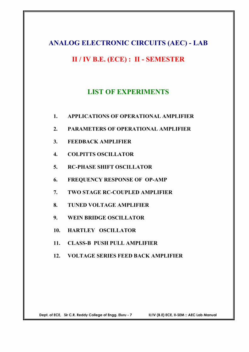
ANALOG ELECTRONIC CIRCUITS (AEC) - LAB
II / IV B.E. (ECE) : II - SEMESTER
LIST OF EXPERIMENTS
1. APPLICATIONS OF OPERATIONAL AMPLIFIER
2. PARAMETERS OF OPERATIONAL AMPLIFIER
3. FEEDBACK AMPLIFIER
4. COLPITTS OSCILLATOR
5. RC-PHASE SHIFT OSCILLATOR
6. FREQUENCY RESPONSE OF OP-AMP
7. TWO STAGE RC-COUPLED AMPLIFIER
8. TUNED VOLTAGE AMPLIFIER
9. WEIN BRIDGE OSCILLATOR
10. HARTLEY OSCILLATOR
11. CLASS-B PUSH PULL AMPLIFIER
12. VOLTAGE SERIES FEED BACK AMPLIFIER
Dept. of ECE, Sir C.R. Reddy College of Engg. Eluru - 7 II/IV (B.E) ECE, II-SEM :: AEC Lab Manual
APPLICATIONS OF
OPERATIONAL AMPLIFIER
Dept. of ECE, Sir C.R. Reddy College of Engg. Eluru - 7 II/IV (B.E) ECE, II-SEM :: AEC Lab Manual
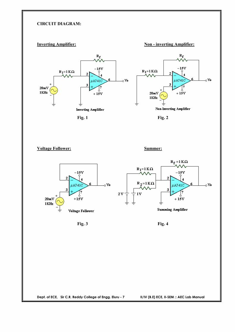
CIRCUIT DIAGRAM:
Inverting Amplifier: Non - inverting Amplifier:
Fig. 1 Fig. 2
Voltage Follower: Summer:
Fig. 3 Fig. 4
Dept. of ECE, Sir C.R. Reddy College of Engg. Eluru - 7 II/IV (B.E) ECE, II-SEM :: AEC Lab Manual
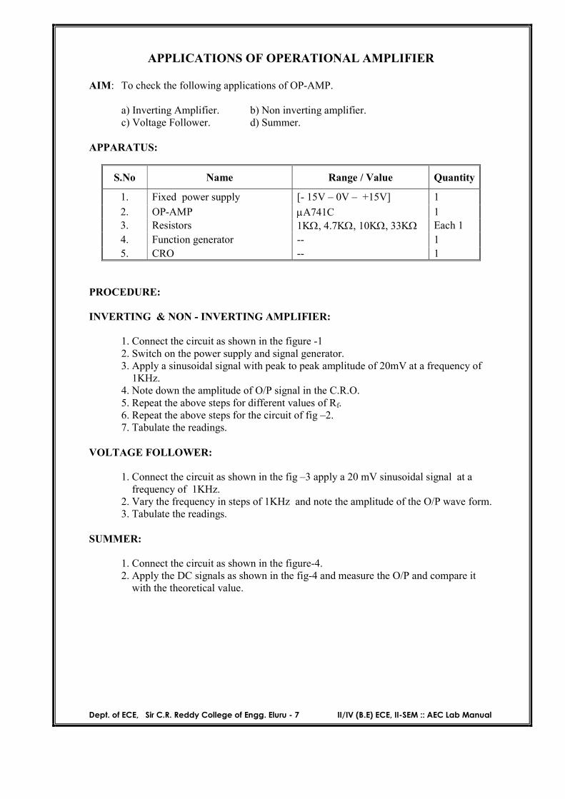
APPLICATIONS OF OPERATIONAL AMPLIFIER
AIM: To check the following applications of OP-AMP. a) Inverting Amplifier. b) Non inverting amplifier. c) Voltage Follower. d) Summer. APPARATUS:
PROCEDURE: INVERTING & NON - INVERTING AMPLIFIER:
1. Connect the circuit as shown in the figure -1 2. Switch on the power supply and signal generator. 3. Apply a sinusoidal signal with peak to peak amplitude of 20mV at a frequency of 1KHz. 4. Note down the amplitude of O/P signal in the C.R.O. 5. Repeat the above steps for different values of Rf. 6. Repeat the above steps for the circuit of fig –2. 7. Tabulate the readings.
VOLTAGE FOLLOWER:
1. Connect the circuit as shown in the fig –3 apply a 20 mV sinusoidal signal at a frequency of 1KHz. 2. Vary the frequency in steps of 1KHz and note the amplitude of the O/P wave form. 3. Tabulate the readings.
SUMMER:
1. Connect the circuit as shown in the figure-4. 2. Apply the DC signals as shown in the fig-4 and measure the O/P and compare it with the theoretical value.
S.No Name Range / Value Quantity
1. Fixed power supply [- 15V – 0V – +15V] 1
2. OP-AMP A741C 1
3. Resistors 1K, 4.7K, 10K, 33K Each 1
4. Function generator -- 1
5. CRO -- 1
Dept. of ECE, Sir C.R. Reddy College of Engg. Eluru - 7 II/IV (B.E) ECE, II-SEM :: AEC Lab Manual
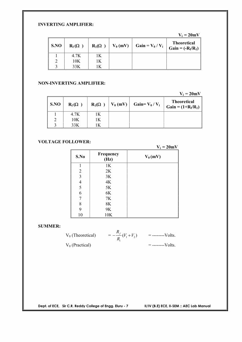
INVERTING AMPLIFIER:
Vi = 20mV
S.NO Rf ( ) R1( ) V0 (mV) Gain = V0 / Vi Theoretical
Dept. of ECE, Sir C.R. Reddy College of Engg. Eluru - 7 II/IV (B.E) ECE, II-SEM :: AEC Lab Manual
RESULT: VIVA QUESTIONS:
1. What are the ideal Characteristics of an OP-AMP ? 2. Explain the concept of virtual ground? 3. What are the internal stages in an OP-AMP IC ? 4. What type of transistor Configuration is used at the front end of an OP-AMP IC ? 5. Draw the circuit diagram of an integrator and a differentiator using an OP-AMP ? 6. Why square wave is used to test any amplifier ?
***
Dept. of ECE, Sir C.R. Reddy College of Engg. Eluru - 7 II/IV (B.E) ECE, II-SEM :: AEC Lab Manual
Dept. of ECE, Sir C.R. Reddy College of Engg. Eluru - 7 II/IV (B.E) ECE, II-SEM :: AEC Lab Manual
PARAMETERS OF OPERATIONAL AMPLIFIER
Dept. of ECE, Sir C.R. Reddy College of Engg. Eluru - 7 II/IV (B.E) ECE, II-SEM :: AEC Lab Manual
Dept. of ECE, Sir C.R. Reddy College of Engg. Eluru - 7 II/IV (B.E) ECE, II-SEM :: AEC Lab Manual
PARAMETERS OF OPERATIONAL AMPLIFIER
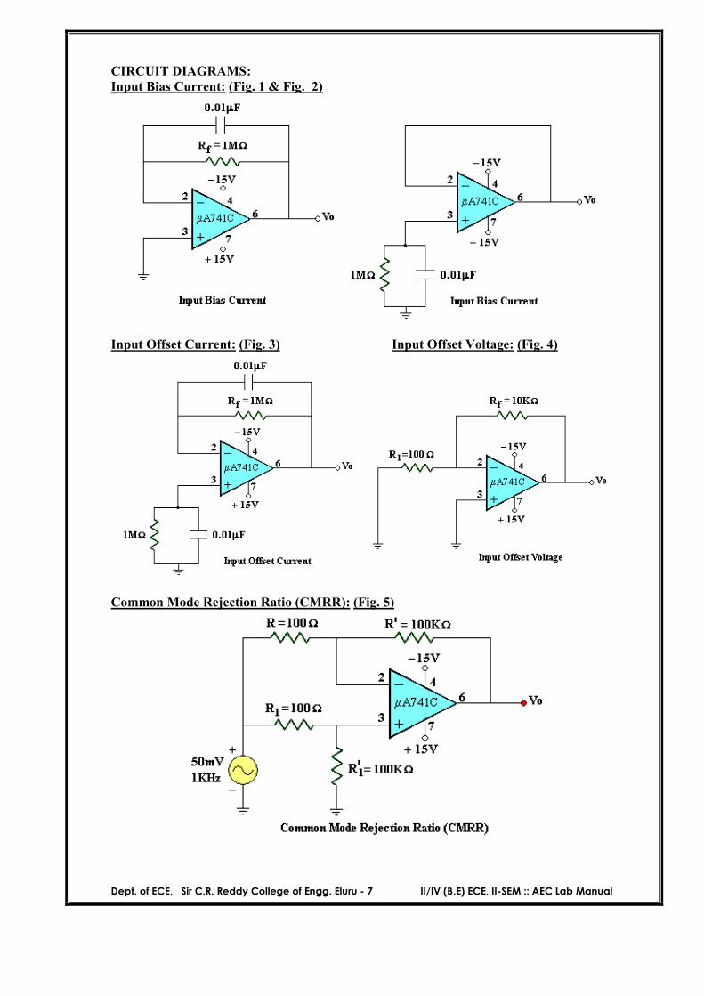
AIM: To determine the following parameters of OP-AMP A741 C. a) Input Bias Current. b) Input Offset Current. c) Input Offset Voltage. d) CMRR. APPARATUS:
PROCEDURE:
1. Connect the circuit as shown in the figure (1). 2. The O/P voltage V0 is measured from the O/P terminals.
3 BI is calculated by using 0
B
f
VI
R .
4. The circuit is connected as shown in the figure (2). 5. The O/P voltage V0 is measured from the O/P terminals.
6. IB+ is calculated by using 0
1
B
VI
R .
7. Input bias current 2
B BB
I II
.
8. The circuit is connected as shown in the figure (3). 9. The Input offset current is measured by using the formula
0io
f
VI
R .The circuit is connected as shown in the figure (4).
10. Input offset voltage
0
1
1io
f
VV
R
R
11. The circuit is connected as shown in the figure (5). 12. A 50 mV sinusoidal signal at a frequency of 1 KHz is applied at the I / P. 13. The O/P voltage V0 is measured. 14. The CMRR is found by using,
1
1 S
O
VRCMRR
R V
.
15. CMRR in decibels = 20log (CMRR).
S.No Name Range / Value Quantity
1. Fixed Power supply [- 15V – 0V – +15V] 1
2. Operational Amplifier A 741C 1
3. Resistors 1M, 10K, 100K, 100 Each 1
4. Capacitors 0.01 F 1 5. Function generator -- 1 6. Multimeter -- 1 7. CRO -- 1
Dept. of ECE, Sir C.R. Reddy College of Engg. Eluru - 7 II/IV (B.E) ECE, II-SEM :: AEC Lab Manual
RESULT: VIVA QUESTIONS:
1. What are the different parameters of an OP-AMP? 2. Define input offset voltage? 3. Define Input bias current and Input offset current? 4. What is meant by slew rate? 5. Why we need to calculate the offset values?
***
Dept. of ECE, Sir C.R. Reddy College of Engg. Eluru - 7 II/IV (B.E) ECE, II-SEM :: AEC Lab Manual
FEEDBACK AMPLIFIER
Dept. of ECE, Sir C.R. Reddy College of Engg. Eluru - 7 II/IV (B.E) ECE, II-SEM :: AEC Lab Manual
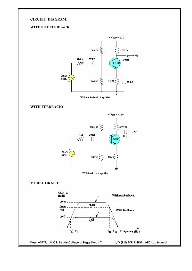
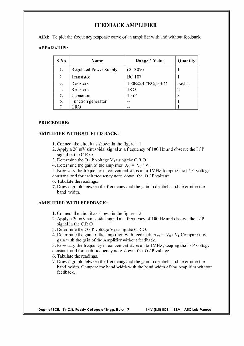
CIRCUIT DIAGRAM:
WITHOUT FEEDBACK:
WITH FEEDBACK:
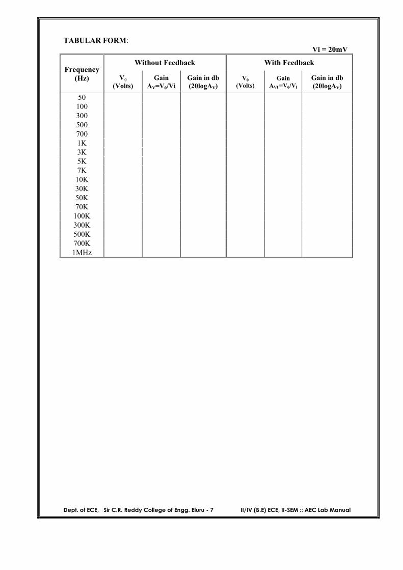
MODEL GRAPH:
Dept. of ECE, Sir C.R. Reddy College of Engg. Eluru - 7 II/IV (B.E) ECE, II-SEM :: AEC Lab Manual
FEEDBACK AMPLIFIER
AIM: To plot the frequency response curve of an amplifier with and without feedback. APPARATUS: PROCEDURE: AMPLIFIER WITHOUT FEED BACK:
1. Connect the circuit as shown in the figure – 1. 2. Apply a 20 mV sinusoidal signal at a frequency of 100 Hz and observe the I / P signal in the C.R.O. 3. Determine the O / P voltage V0 using the C.R.O. 4. Determine the gain of the amplifier AV = V0 / VI . 5. Now vary the frequency in convenient steps upto 1MHz, keeping the I / P voltage constant and for each frequency note down the O / P voltage. 6. Tabulate the readings. 7. Draw a graph between the frequency and the gain in decibels and determine the band width.
AMPLIFIER WITH FEEDBACK:
1. Connect the circuit as shown in the figure – 2. 2. Apply a 20 mV sinusoidal signal at a frequency of 100 Hz and observe the I / P signal in the C.R.O. 3. Determine the O / P voltage V0 using the C.R.O. 4. Determine the gain of the amplifier with feedback AVf = V0 / VI .Compare this gain with the gain of the Amplifier without feedback. 5. Now vary the frequency in convenient steps up to 1MHz ,keeping the I / P voltage constant and for each frequency note down the O / P voltage. 6. Tabulate the readings. 7. Draw a graph between the frequency and the gain in decibels and determine the band width. Compare the band width with the band width of the Amplifier without feedback.
Dept. of ECE, Sir C.R. Reddy College of Engg. Eluru - 7 II/IV (B.E) ECE, II-SEM :: AEC Lab Manual
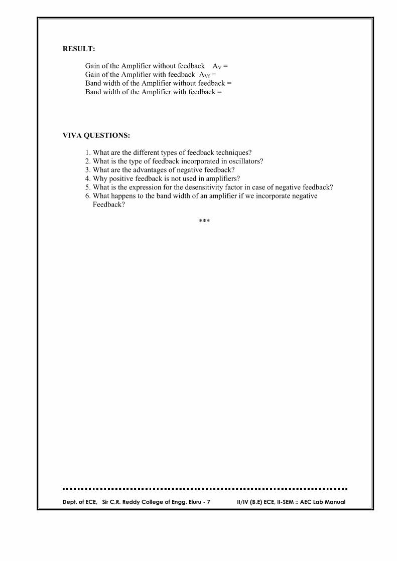
TABULAR FORM: Vi = 20mV
Frequency (Hz)
Without Feedback With Feedback
V0
(Volts) Gain
AV=V0/Vi Gain in db (20logAV)
V0
(Volts) Gain
AVf =V0/VI Gain in db (20logAV)
50 100 300 500 700 1K 3K 5K 7K
10K 30K 50K 70K 100K 300K 500K 700K 1MHz
Dept. of ECE, Sir C.R. Reddy College of Engg. Eluru - 7 II/IV (B.E) ECE, II-SEM :: AEC Lab Manual
RESULT:
Gain of the Amplifier without feedback AV = Gain of the Amplifier with feedback AVf = Band width of the Amplifier without feedback = Band width of the Amplifier with feedback =
VIVA QUESTIONS:
1. What are the different types of feedback techniques? 2. What is the type of feedback incorporated in oscillators? 3. What are the advantages of negative feedback? 4. Why positive feedback is not used in amplifiers? 5. What is the expression for the desensitivity factor in case of negative feedback? 6. What happens to the band width of an amplifier if we incorporate negative
Feedback?
***
Dept. of ECE, Sir C.R. Reddy College of Engg. Eluru - 7 II/IV (B.E) ECE, II-SEM :: AEC Lab Manual
Dept. of ECE, Sir C.R. Reddy College of Engg. Eluru - 7 II/IV (B.E) ECE, II-SEM :: AEC Lab Manual
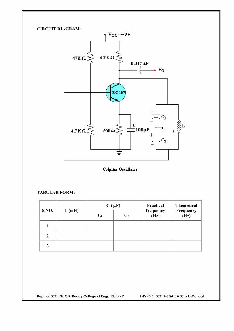
COLPITTS OSCILLATOR
Dept. of ECE, Sir C.R. Reddy College of Engg. Eluru - 7 II/IV (B.E) ECE, II-SEM :: AEC Lab Manual
CIRCUIT DIAGRAM:
TABULAR FORM:
S.NO. L (mH) C ( F) Practical
frequency (Hz)
Theoretical Frequency
(Hz) C1 C2
1
2
3
Dept. of ECE, Sir C.R. Reddy College of Engg. Eluru - 7 II/IV (B.E) ECE, II-SEM :: AEC Lab Manual
COLPITTS OSCILLATOR
AIM: To determine the frequency of oscillations of a given Colpitts Oscillator. APPARATUS: PROCEDURE:
1. Connect the circuit diagram as shown in the figure. 2. Switch on the power supply. 3. Connect the out put terminals to CRO. 4. Adjust the capacitances until a sinusoidal wave form is observed on the
CRO. 5. Measure the time period of the sinusoidal wave form (T) and determine the Frequency (1/T). 6. Repeat the above steps for different values of L, C1 & C2. 7. Tabulate the readings and compare with theoretical values
CALCULATIONS:
f0 (practical) =1/T Hz.
f0 (theoretical) 0
1
2 eq
fLC
. [Where 1 2
1 2
eq
C CC
C C
]
RESULT: VIVA QUESTIONS:
1. Why RC network oscillator cannot be used at Radio frequencies? 2. Why LC network oscillators are preferred at high frequencies? 3. Why a buffer amplifier is required in between an oscillator and a load? 4. What is meant by ringing in an amplifier? 5. Why the crystal oscillator is highly stable? 6. Draw the electrical equivalent circuit of a crystal oscillator?
***
S.No Name Range / Value Quantity
1. DC Regulated Power Supply (0-30V) 1 2. Resistors 560, 47 K Each 1
Dept. of ECE, Sir C.R. Reddy College of Engg. Eluru - 7 II/IV (B.E) ECE, II-SEM :: AEC Lab Manual
Dept. of ECE, Sir C.R. Reddy College of Engg. Eluru - 7 II/IV (B.E) ECE, II-SEM :: AEC Lab Manual
RC-PHASE SHIFT OSCILLATOR
Dept. of ECE, Sir C.R. Reddy College of Engg. Eluru - 7 II/IV (B.E) ECE, II-SEM :: AEC Lab Manual
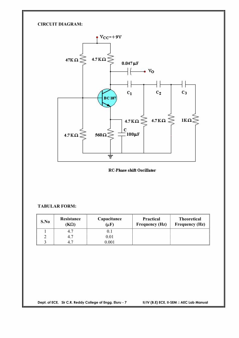
CIRCUIT DIAGRAM:
TABULAR FORM:
S.No Resistance
(K) Capacitance
(F) Practical
Frequency (Hz) Theoretical
Frequency (Hz)
1 4.7 0.1 2 4.7 0.01 3 4.7 0.001
Dept. of ECE, Sir C.R. Reddy College of Engg. Eluru - 7 II/IV (B.E) ECE, II-SEM :: AEC Lab Manual
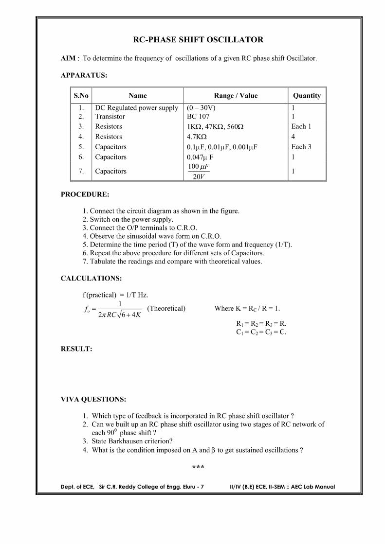
RC-PHASE SHIFT OSCILLATOR
AIM : To determine the frequency of oscillations of a given RC phase shift Oscillator. APPARATUS:
PROCEDURE:
1. Connect the circuit diagram as shown in the figure. 2. Switch on the power supply. 3. Connect the O/P terminals to C.R.O. 4. Observe the sinusoidal wave form on C.R.O. 5. Determine the time period (T) of the wave form and frequency (1/T). 6. Repeat the above procedure for different sets of Capacitors. 7. Tabulate the readings and compare with theoretical values.
CALCULATIONS:
f (practical) = 1/T Hz. 1
2 6 4of
RC K
(Theoretical) Where K = RC / R = 1.
R1 = R2 = R3 = R. C1 = C2 = C3 = C.
RESULT: VIVA QUESTIONS:
1. Which type of feedback is incorporated in RC phase shift oscillator ? 2. Can we built up an RC phase shift oscillator using two stages of RC network of
each 900 phase shift ?
3. State Barkhausen criterion? 4. What is the condition imposed on A and to get sustained oscillations ?
***
S.No Name Range / Value Quantity
1. DC Regulated power supply (0 – 30V) 1 2. Transistor BC 107 1
3. Resistors 1K, 47K, 560 Each 1
4. Resistors 4.7K 4
5. Capacitors 0.1F, 0.01F, 0.001F Each 3
6. Capacitors 0.047 F 1
7. Capacitors V
F
20
100 1
Dept. of ECE, Sir C.R. Reddy College of Engg. Eluru - 7 II/IV (B.E) ECE, II-SEM :: AEC Lab Manual
Dept. of ECE, Sir C.R. Reddy College of Engg. Eluru - 7 II/IV (B.E) ECE, II-SEM :: AEC Lab Manual
FREQUENCY RESPONSE OF OP-AMP
Dept. of ECE, Sir C.R. Reddy College of Engg. Eluru - 7 II/IV (B.E) ECE, II-SEM :: AEC Lab Manual
Dept. of ECE, Sir C.R. Reddy College of Engg. Eluru - 7 II/IV (B.E) ECE, II-SEM :: AEC Lab Manual
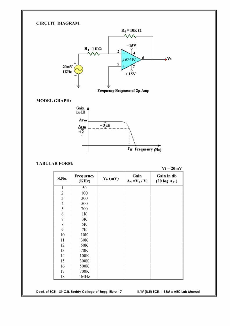
FREQUENCY RESPONSE OF OP-AMP
AIM: To plot the frequency response characteristics of OP-AMP A 741 C and to obtain the band width.
APPARATUS:
PROCEDURE:
1. Connect the circuit as shown in the figure. 2. Switch on the power supply and the function generator. 3. Apply a 20 mV sinusoidal signal at the I/P. 4. Vary the frequency in convenient steps and note down the amplitude of the O/P
Wave form. 5. Tabulate the readings. 6. Plot a graph between gain and frequency. 7. Determine the band width.
RESULT: Upper cut-off frequency = KHz. Lower cut-off frequency = Hz. Band Width = KHz
***
S.No Name Range / Value Quantity
1. Fixed power supply [- 15V – 0V – +15V] 1 2. OP-AMP A 741 C 1
3. Resistors 10K, 1K Each 1 4. Function generator -- 1 5. CRO -- 1
Dept. of ECE, Sir C.R. Reddy College of Engg. Eluru - 7 II/IV (B.E) ECE, II-SEM :: AEC Lab Manual
Dept. of ECE, Sir C.R. Reddy College of Engg. Eluru - 7 II/IV (B.E) ECE, II-SEM :: AEC Lab Manual
TWO STAGE RC-COUPLED AMPLIFIER
Dept. of ECE, Sir C.R. Reddy College of Engg. Eluru - 7 II/IV (B.E) ECE, II-SEM :: AEC Lab Manual
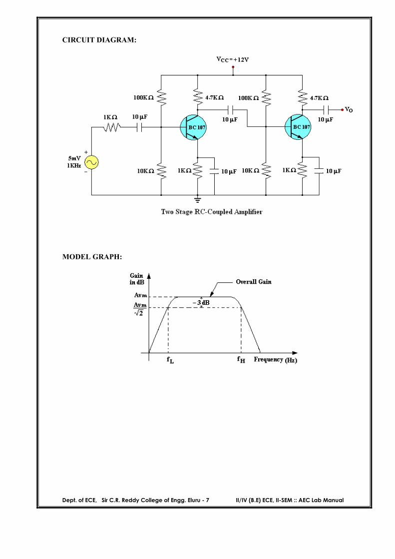
CIRCUIT DIAGRAM:
MODEL GRAPH:
Dept. of ECE, Sir C.R. Reddy College of Engg. Eluru - 7 II/IV (B.E) ECE, II-SEM :: AEC Lab Manual
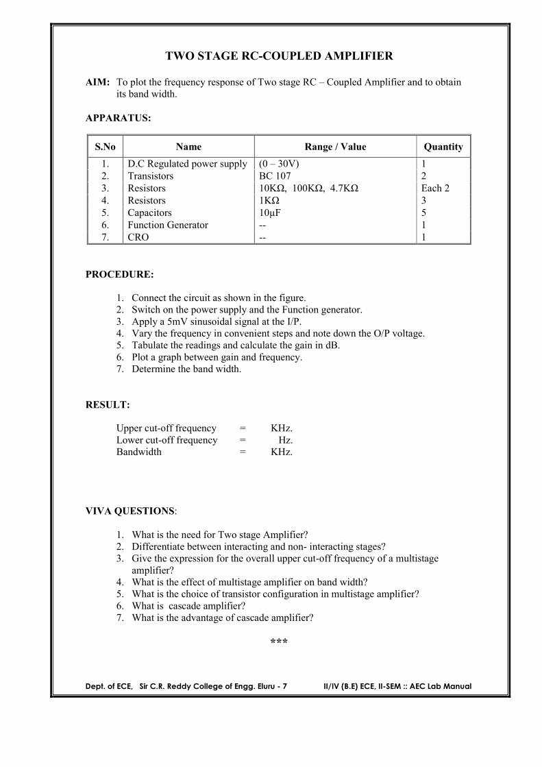
TWO STAGE RC-COUPLED AMPLIFIER
AIM: To plot the frequency response of Two stage RC – Coupled Amplifier and to obtain its band width.
APPARATUS:
PROCEDURE:
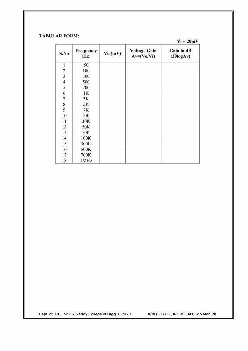
1. Connect the circuit as shown in the figure. 2. Switch on the power supply and the Function generator. 3. Apply a 5mV sinusoidal signal at the I/P. 4. Vary the frequency in convenient steps and note down the O/P voltage. 5. Tabulate the readings and calculate the gain in dB. 6. Plot a graph between gain and frequency. 7. Determine the band width.
RESULT:
Upper cut-off frequency = KHz. Lower cut-off frequency = Hz. Bandwidth = KHz.
VIVA QUESTIONS:
1. What is the need for Two stage Amplifier? 2. Differentiate between interacting and non- interacting stages? 3. Give the expression for the overall upper cut-off frequency of a multistage
amplifier? 4. What is the effect of multistage amplifier on band width? 5. What is the choice of transistor configuration in multistage amplifier? 6. What is cascade amplifier? 7. What is the advantage of cascade amplifier?
***
S.No Name Range / Value Quantity
1. D.C Regulated power supply (0 – 30V) 1 2. Transistors BC 107 2 3. Resistors 10KΩ, 100KΩ, 4.7KΩ Each 2 4. Resistors 1KΩ 3 5. Capacitors 10µF 5 6. Function Generator -- 1 7. CRO -- 1
Dept. of ECE, Sir C.R. Reddy College of Engg. Eluru - 7 II/IV (B.E) ECE, II-SEM :: AEC Lab Manual
Dept. of ECE, Sir C.R. Reddy College of Engg. Eluru - 7 II/IV (B.E) ECE, II-SEM :: AEC Lab Manual
WEIN BRIDGE OSCILLATOR
Dept. of ECE, Sir C.R. Reddy College of Engg. Eluru - 7 II/IV (B.E) ECE, II-SEM :: AEC Lab Manual
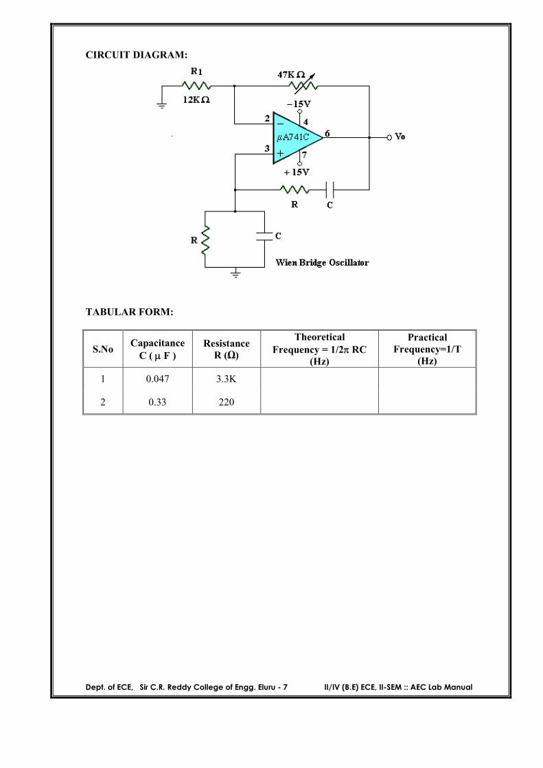
CIRCUIT DIAGRAM:
TABULAR FORM:
S.No Capacitance
C ( F ) Resistance
R (Ω)
Theoretical Frequency = 1/2 RC
(Hz)
Practical Frequency=1/T
(Hz)
1 0.047 3.3K
2 0.33 220
Dept. of ECE, Sir C.R. Reddy College of Engg. Eluru - 7 II/IV (B.E) ECE, II-SEM :: AEC Lab Manual
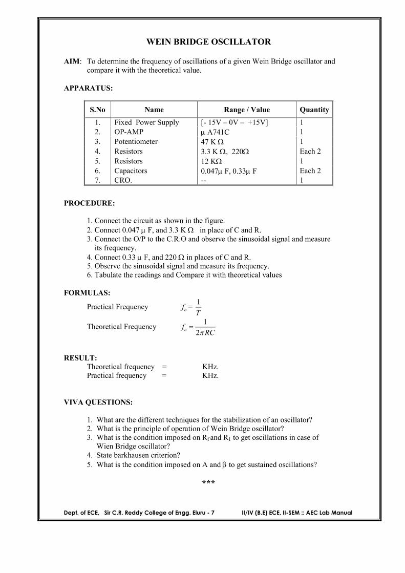
WEIN BRIDGE OSCILLATOR
AIM: To determine the frequency of oscillations of a given Wein Bridge oscillator and compare it with the theoretical value.
APPARATUS: PROCEDURE:
1. Connect the circuit as shown in the figure. 2. Connect 0.047 F, and 3.3 K in place of C and R. 3. Connect the O/P to the C.R.O and observe the sinusoidal signal and measure its frequency. 4. Connect 0.33 F, and 220 in places of C and R. 5. Observe the sinusoidal signal and measure its frequency. 6. Tabulate the readings and Compare it with theoretical values
FORMULAS:
Practical Frequency of = T
1
Theoretical Frequency 1
2of
RC
RESULT: Theoretical frequency = KHz. Practical frequency = KHz.
VIVA QUESTIONS:
1. What are the different techniques for the stabilization of an oscillator? 2. What is the principle of operation of Wein Bridge oscillator? 3. What is the condition imposed on Rf and R1 to get oscillations in case of Wien Bridge oscillator? 4. State barkhausen criterion? 5. What is the condition imposed on A and to get sustained oscillations?
Dept. of ECE, Sir C.R. Reddy College of Engg. Eluru - 7 II/IV (B.E) ECE, II-SEM :: AEC Lab Manual
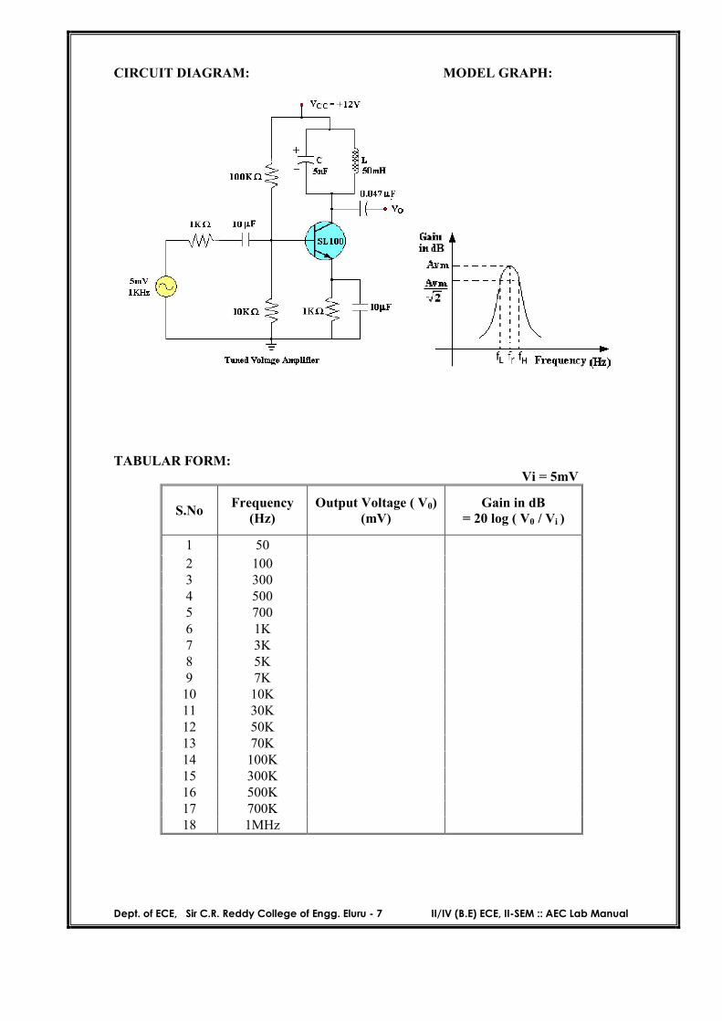
TUNED VOLTAGE AMPLIFIER
AIM: To obtain the frequency response of a tuned voltage amplifier. and to obtain the band width. APPARATUS:
PROCEDURE:
1. Connect the circuit as shown in the figure. 2. Apply a 4 mV sinusoidal signal at a frequency of 1 KHz and note down the O/P. 3. Now vary the frequency of the input signal upto 1MHz in suitable steps by keeping
the input voltage constant. 4. Note down the O/P voltage V0. 5. Tabulate the readings. 6. Draw gain Vs frequency graph on semi log sheet and determine the band width.
RESULT: VIVA QUESTIONS:
1. What is a tuned amplifier? 2. Distinguish between a single tuned and a double tuned amplifier? 3. What is meant by stagger tuned amplifier? 4. Is the tuned amplifier a narrow band or a wide band amplifier? 5. Define selectivity? 6. What parameters shall be selected for a highly tuned amplifier? 7. Where the tuned amplifiers are used? 8. What type of tuning is used in the IF stage of a Radio receiver ? 9. What is the relation between the band width of a double tuned and a stagger tuned amplifier? 10. How to improve the band width of a tuned amplifier? 11. What is meant by critical tuning?
***
S.No Name Range / Value Quantity
1. Transistor SL100 1 2. Resistors 1K , 22 K , 1.8K, 470 Each 1 3. Capacitors 10F, 33F Each 1 4. IF Transformer -- 1
Dept. of ECE, Sir C.R. Reddy College of Engg. Eluru - 7 II/IV (B.E) ECE, II-SEM :: AEC Lab Manual
Dept. of ECE, Sir C.R. Reddy College of Engg. Eluru - 7 II/IV (B.E) ECE, II-SEM :: AEC Lab Manual
HARTLEY OSCILLATOR
Dept. of ECE, Sir C.R. Reddy College of Engg. Eluru - 7 II/IV (B.E) ECE, II-SEM :: AEC Lab Manual
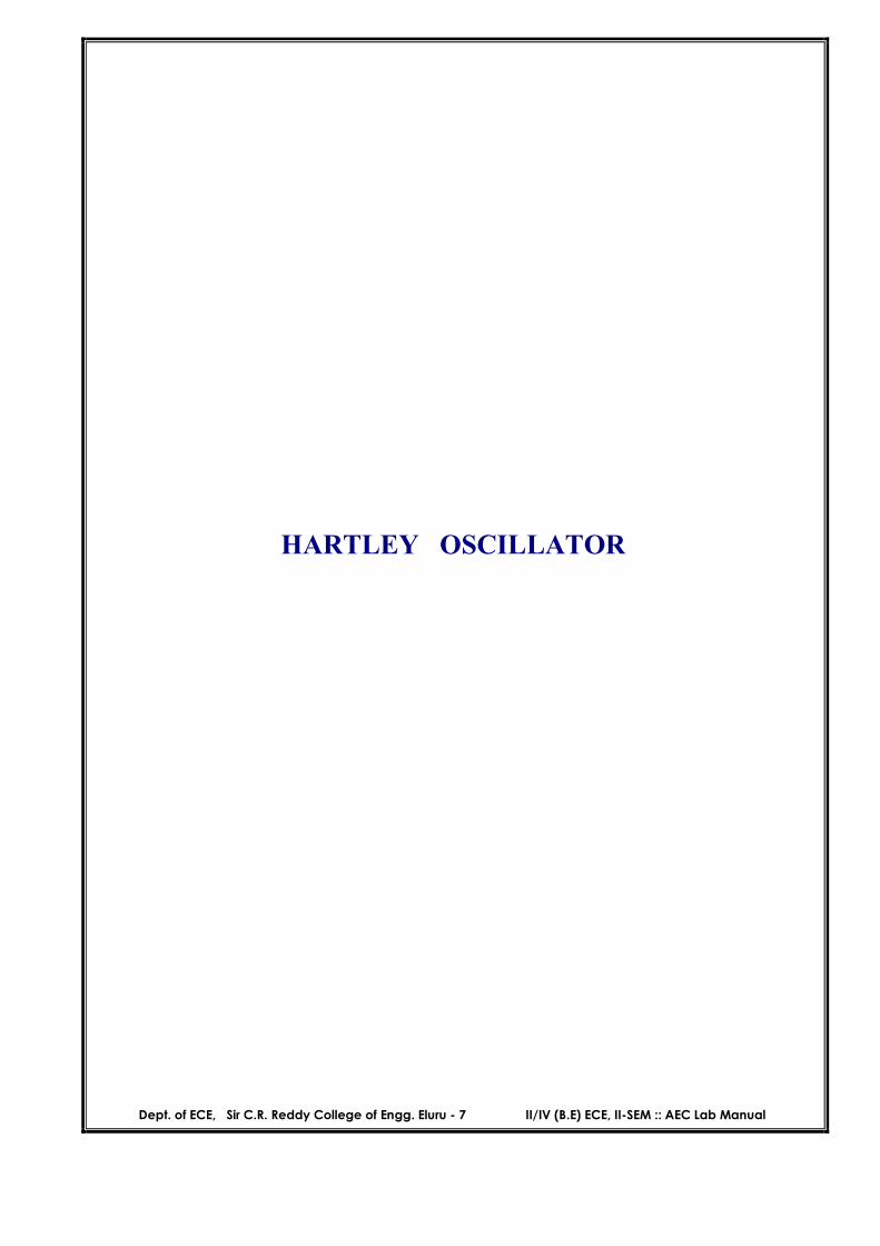
CIRCUIT DIAGRAM:
TABULAR FORM:
Capacitance C ( F )
Inductance ( m H ) Practical
Frequency (Hz) Theoretical
Frequency (Hz) L 1 L 2
Dept. of ECE, Sir C.R. Reddy College of Engg. Eluru - 7 II/IV (B.E) ECE, II-SEM :: AEC Lab Manual
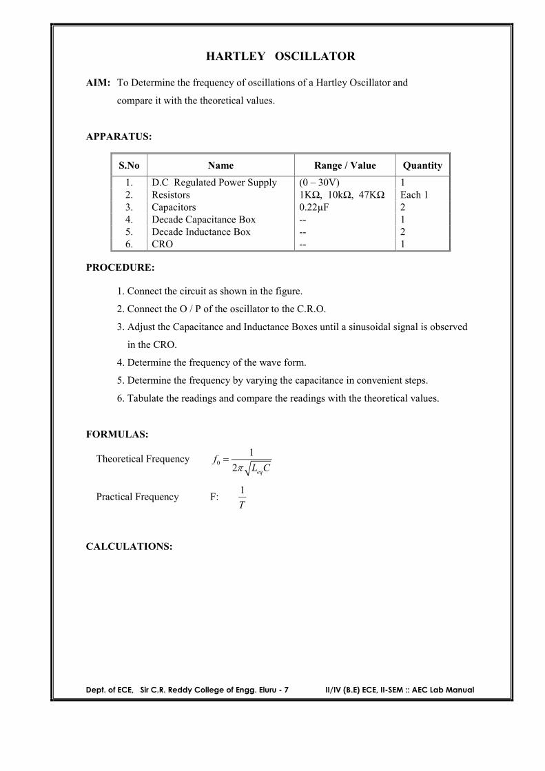
HARTLEY OSCILLATOR
AIM: To Determine the frequency of oscillations of a Hartley Oscillator and
compare it with the theoretical values.
APPARATUS: PROCEDURE:
1. Connect the circuit as shown in the figure.
2. Connect the O / P of the oscillator to the C.R.O.
3. Adjust the Capacitance and Inductance Boxes until a sinusoidal signal is observed
in the CRO.
4. Determine the frequency of the wave form.
5. Determine the frequency by varying the capacitance in convenient steps.
6. Tabulate the readings and compare the readings with the theoretical values.
Dept. of ECE, Sir C.R. Reddy College of Engg. Eluru - 7 II/IV (B.E) ECE, II-SEM :: AEC Lab Manual
RESULT: VIVA QUESTIONS:
1. Why RC network oscillator cannot be used at Radio frequencies?
2. Why LC network oscillators are preferred at high frequencies?
3. Why a buffer amplifier is required in between an oscillator and a load?
4. What is meant by ringing in an amplifier?
5. Why the crystal oscillator is highly stable?
6. Draw the electrical equivalent circuit of a crystal oscillator?
***
Dept. of ECE, Sir C.R. Reddy College of Engg. Eluru - 7 II/IV (B.E) ECE, II-SEM :: AEC Lab Manual
CLASS-B PUSH PULL AMPLIFIER
Dept. of ECE, Sir C.R. Reddy College of Engg. Eluru - 7 II/IV (B.E) ECE, II-SEM :: AEC Lab Manual
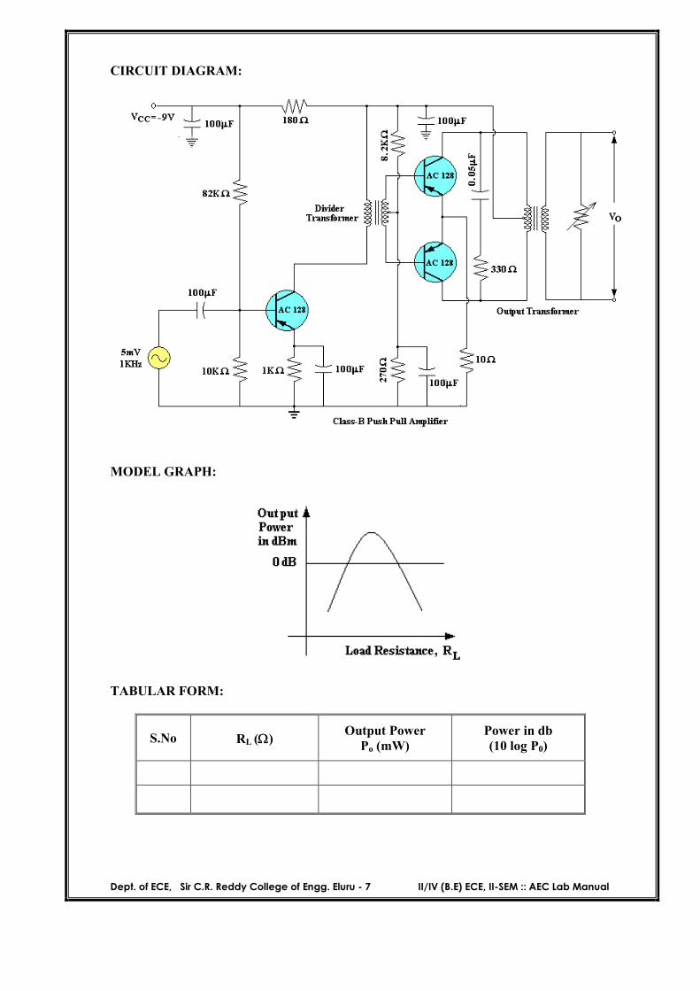
CIRCUIT DIAGRAM:
MODEL GRAPH:
TABULAR FORM:
S.No RL () Output Power
Po (mW) Power in db (10 log P0)
Dept. of ECE, Sir C.R. Reddy College of Engg. Eluru - 7 II/IV (B.E) ECE, II-SEM :: AEC Lab Manual
CLASS-B PUSH PULL AMPLIFIER
AIM: To Plot the Graph between Load and Power of a Class B Push pull Power Amplifier. APPARATUS:
PROCEDURE:
1. Connect the circuit diagram as shown in the figure. 2. Determine the maximum signal handling capacity of the push pull amplifier. 3. Apply sinusoidal signal of 4mV peak to peak voltage at a frequency of 1 KHz. 4. Connect Power meter at the O/P terminals. 5. By changing the load at the O/P terminals measure the power in the Power meter. 6. Tabulate the readings. 7. plot the graph between Power vs load
RESULT: VIVA QUESTIONS:
1. What is meant by conversion efficiency? Which type of power amplifier has the maximum conversion efficiency? Why?
2. To which class does the push-pull amplifier belongs and what are the advantages of it? 3. What is meant by crossover distortion? In which power amplifier it is maximum? 4. Why class-A amplifier is used in transmitter modulators? 5. What is the maximum theoretical efficiency of a class-A amplifier? 6. Which harmonics are eliminated in the class –B push-pull amplifier? 7. What is meant by complementary symmetry push-pull amplifier? State its
advantages. 8. Why the load is to be coupled through a transformer in a class-A amplifier? 9. Discuss the stability techniques of power amplifier? 10. Draw the thermal equivalent circuit of a power amplifier?
***
S.No Name Range / Value Quantity
1. Push pull power amplifier module -- 1 2. D.C Regulated Power supply (0-30V). 1 3. Function generator -- 1
4. CRO -- 1
Dept. of ECE, Sir C.R. Reddy College of Engg. Eluru - 7 II/IV (B.E) ECE, II-SEM :: AEC Lab Manual
Dept. of ECE, Sir C.R. Reddy College of Engg. Eluru - 7 II/IV (B.E) ECE, II-SEM :: AEC Lab Manual
VOLTAGE SERIES FEED BACK AMPLIFIER
Dept. of ECE, Sir C.R. Reddy College of Engg. Eluru - 7 II/IV (B.E) ECE, II-SEM :: AEC Lab Manual
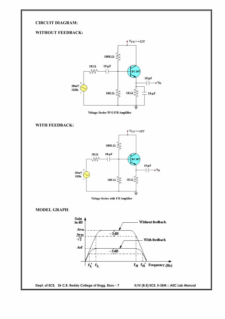
CIRCUIT DIAGRAM: WITHOUT FEEDBACK:
WITH FEEDBACK:
MODEL GRAPH:
Dept. of ECE, Sir C.R. Reddy College of Engg. Eluru - 7 II/IV (B.E) ECE, II-SEM :: AEC Lab Manual
VOLTAGE SERIES FEED BACK AMPLIFIER
AIM: To Plot the frequency response curve of an amplifier with and without feedback. APPARATUS:
1. Connect the circuit as shown in figure – 1. 2. Apply a 20mV sinusoidal signal at a frequency of 100Hz and observe the I/P
waveform in the CRO. 3. Determine the O/P Voltage Vo using the CRO. 4. Determine the gain of the amplifier Av = Vo/Vi. 5. Now vary the frequency in convenient steps up to 1MHz keeping the I/P constant
and for each frequency note down the O/P voltage. 6. Tabulate the readings. 7. Draw the graph between the frequency and the gain in decibels and determine the
band width. AMPLIFIER WITH FEEDBACK: 1. Connect the circuit as shown in figure – 2.
2. Apply a 20mV sinusoidal signal at a frequency of 100Hz and observe the I/P waveform in the CRO.
3. Determine the O/P Voltage Vo using the CRO. 4. Determine the gain of the amplifier Avf = Vo/Vi. Compare this gain with the gain
of the Amplifier without feedback. 5. Now vary the frequency in convenient steps up to 1MHz keeping the I/P constant
and for each frequency note down the O/P voltage. 6. Tabulate the readings. 7. Draw the graph between the frequency and the gain in decibels and determine the
band width. Compare the band width with the band width of the Amplifier without feedback.
Dept. of ECE, Sir C.R. Reddy College of Engg. Eluru - 7 II/IV (B.E) ECE, II-SEM :: AEC Lab Manual
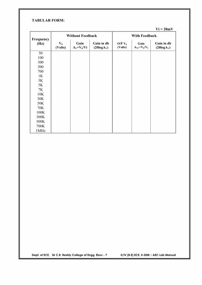
TABULAR FORM: Vi = 20mV
Frequency (Hz)
Without Feedback With Feedback
V0
(Volts) Gain
AV=V0/Vi Gain in db (20logAV)
O/P V0
(Volts) Gain
AVf =V0/VI Gain in db (20logAV)
50 100 300 500 700 1K 3K 5K 7K 10K 30K 50K 70K
100K 300K 500K 700K 1MHz
Dept. of ECE, Sir C.R. Reddy College of Engg. Eluru - 7 II/IV (B.E) ECE, II-SEM :: AEC Lab Manual
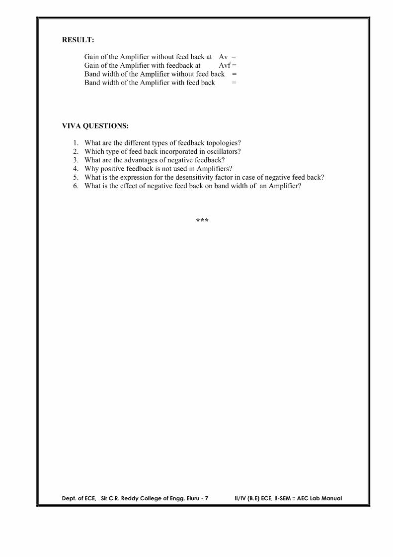
RESULT:
Gain of the Amplifier without feed back at Av = Gain of the Amplifier with feedback at Avf = Band width of the Amplifier without feed back = Band width of the Amplifier with feed back = VIVA QUESTIONS:
1. What are the different types of feedback topologies? 2. Which type of feed back incorporated in oscillators? 3. What are the advantages of negative feedback? 4. Why positive feedback is not used in Amplifiers? 5. What is the expression for the desensitivity factor in case of negative feed back? 6. What is the effect of negative feed back on band width of an Amplifier?
***
Dept. of ECE, Sir C.R. Reddy College of Engg. Eluru - 7 II/IV (B.E) ECE, II-SEM :: AEC Lab Manual