21
Analogue Devices and Techniques Amplifier Design Gavin Cameron MSc/PGD Electronics and Communication Engineering February 8, 2000

Analogue Devices and Techniques
Amplifier Design
Gavin Cameron
MSc/PGD Electronics and Communication Engineering
February 8, 2000

Gavin Cameron, February 8, 2000 Page 2 of 21
TABLE OF CONTENTSLIST OF TABLES AND FIGURES . . . . . . . . . . . . . . . . . . . . . . . . . . . . . . . . . . . . . . . . . . . . . . . . . 3
ABSTRACT . . . . . . . . . . . . . . . . . . . . . . . . . . . . . . . . . . . . . . . . . . . . . . . . . . . . . . . . . . . . . . . . . . . . 4
INTRODUCTION . . . . . . . . . . . . . . . . . . . . . . . . . . . . . . . . . . . . . . . . . . . . . . . . . . . . . . . . . . . . . . . 5
WHAT IS AN OPERATIONAL AMPLIFIER? . . . . . . . . . . . . . . . . . . . . . . . . . . . . . . . . . . . . . . . . 6
AMPLIFIER DESIGN . . . . . . . . . . . . . . . . . . . . . . . . . . . . . . . . . . . . . . . . . . . . . . . . . . . . . . . . . . . . 7
Current Reference. . . . . . . . . . . . . . . . . . . . . . . . . . . . . . . . . . . . . . . . . . . . . . . . . . . . . . . . . . 8
Differential Stage . . . . . . . . . . . . . . . . . . . . . . . . . . . . . . . . . . . . . . . . . . . . . . . . . . . . . . . . . . 8
Gain Stage . . . . . . . . . . . . . . . . . . . . . . . . . . . . . . . . . . . . . . . . . . . . . . . . . . . . . . . . . . . . . . . 9
Output Stage . . . . . . . . . . . . . . . . . . . . . . . . . . . . . . . . . . . . . . . . . . . . . . . . . . . . . . . . . . . . . . 9
AC Analysis . . . . . . . . . . . . . . . . . . . . . . . . . . . . . . . . . . . . . . . . . . . . . . . . . . . . . . . . . . . . . 10
ANALYSIS OF CIRCUIT . . . . . . . . . . . . . . . . . . . . . . . . . . . . . . . . . . . . . . . . . . . . . . . . . . . . . . . . 14
CONCLUSION . . . . . . . . . . . . . . . . . . . . . . . . . . . . . . . . . . . . . . . . . . . . . . . . . . . . . . . . . . . . . . . . 18
REFERENCES. . . . . . . . . . . . . . . . . . . . . . . . . . . . . . . . . . . . . . . . . . . . . . . . . . . . . . . . . . . . . . . . . 19
APPENDIX A - Spice Netlist. . . . . . . . . . . . . . . . . . . . . . . . . . . . . . . . . . . . . . . . . . . . . . . . . . . . . . 20
APPENDIX B - FINAL SCHEMATIC . . . . . . . . . . . . . . . . . . . . . . . . . . . . . . . . . . . . . . . . . . . . . . 21

Gavin Cameron, February 8, 2000 Page 3 of 21
LIST OF TABLES AND FIGURESFigure 1 - Amplifier circuit . . . . . . . . . . . . . . . . . . . . . . . . . . . . . . . . . . . . . . . . . . . . . . . . . . . . . . . . 7
Table 1 - BC337 transistor parameters . . . . . . . . . . . . . . . . . . . . . . . . . . . . . . . . . . . . . . . . . . . . . . . . 7
Table 2 - Gains of stages . . . . . . . . . . . . . . . . . . . . . . . . . . . . . . . . . . . . . . . . . . . . . . . . . . . . . . . . . 14
Figure 2 - DC offset voltages . . . . . . . . . . . . . . . . . . . . . . . . . . . . . . . . . . . . . . . . . . . . . . . . . . . . . . 14
Figure 3 - Differential stage . . . . . . . . . . . . . . . . . . . . . . . . . . . . . . . . . . . . . . . . . . . . . . . . . . . . . . . 15
Figure 4 - Gain stage . . . . . . . . . . . . . . . . . . . . . . . . . . . . . . . . . . . . . . . . . . . . . . . . . . . . . . . . . . . . 15
Figure 5 - Output stage . . . . . . . . . . . . . . . . . . . . . . . . . . . . . . . . . . . . . . . . . . . . . . . . . . . . . . . . . . . 16
Table 3 - Final gains of stages . . . . . . . . . . . . . . . . . . . . . . . . . . . . . . . . . . . . . . . . . . . . . . . . . . . . . 16
Table 3 - Requirements comparison. . . . . . . . . . . . . . . . . . . . . . . . . . . . . . . . . . . . . . . . . . . . . . . . . 18

Gavin Cameron, February 8, 2000 Page 4 of 21
ABSTRACTThis report contains the design of an operational amplifier to meet certain specifications.
It includes all manual calculations which led to the design and simulation results to prove the design.

Gavin Cameron, February 8, 2000 Page 5 of 21
INTRODUCTIONSince the advent of semi-conductors, the world of electronics has greatly advanced. Circuits are becoming smaller, using less power and hence lasting longer, when powered from batteries.
Amplifiers have existed since valve technology, however, nowadays an amplifier can be manufactured onto a single piece of silicon.
Operation Amplifiers (Op-amps) are such devices. They generally have differential inputs and a single ended output with a gain-bandwidth product in the MHz range. Op-amps are constructed with three stages:
1. Differential input stage - high differential gain and common mode rejection
2. Gain stage - high gain
3. Output stage - to increase drive capability
The purpose of this assignment was to design an operational amplifier out of discrete devices.

Gavin Cameron, February 8, 2000 Page 6 of 21
WHAT IS AN OPERATIONAL AMPLIFIER?Operational amplifiers are often used in instrumentation applications, for example sound sensors, motion sensors, temperature sensors etc. The output of the transducers are normally very small, i.e. milli or micro volts.
The transducers are often in electrically noisy environments, like factories and power stations etc. In order to reduce the amount of noise that the wires between the transducer and the op-amp pick up, differential transmission techniques are used. This is normally a twisted pair of wires, with or without shielding. As the wires are twisted together, the average distance between either wire and a noise source is the same. Hence any noise induced in one wire will be induced in the other wire.
Differential amplifiers amplify the difference between the two inputs, hence if the transducer is producing a 1mV differential, but 1V of noise is present on both wires (in phase) then only the true signal will be amplified. This is known as Common Mode Rejection.
Due to the nature of their design, differential amplifiers generally have a gain of up to 1000. For very small signals, this may not be sufficient to be of use to instrumentation, hence, a second stage of amplification is required. This is normally a Darlington type configuration to give a second gain of up to 1000, with more stages added if required. However, the Darlington output is of a very high impedance and as such cannot drive any significant loads.
To increase the drive capability of the amplifier, an output stage is added. There are many different configurations of output stages, for example an emitter follower. The output stage usually has a gain of 1, however, it can drive much larger loads than any other stage.
The stages are usually DC coupled together. This requires that the input of the second stage (for example) provide the bias current for the first stage and so on, so DC offset voltages and bias currents are critical to any design.
The feature of an op-amp that makes it special is the wide variety of ways that it can be used in a circuit. For example, it could be a simple amplifier, an inverting amplifier, a comparator, a differentiator, an integrator, etc.

Gavin Cameron, February 8, 2000 Page 7 of 21
AMPLIFIER DESIGNThe op-amp designed for this experiment is shown in figure 1 below:
Figure 1 - Amplifier circuit
The numbers in circles are the node numbers used later in the report for the Spice netlist.
All transistors are BC337s which were chosen due to the student familiarity with them. They have the following basic parameters:
Table 1 - BC337 transistor parameters
Transistor Type Early Voltage, VA Forward Gain, β Base-Emitter Voltage, VBEBC337 npn 56.7 V 347 0.785 V
The op-amp was designed in 4 stages, firstly the current reference, then differential stage, gain stage and output stage.
Gavin Cameron, February 8, 2000 Page 8 of 21
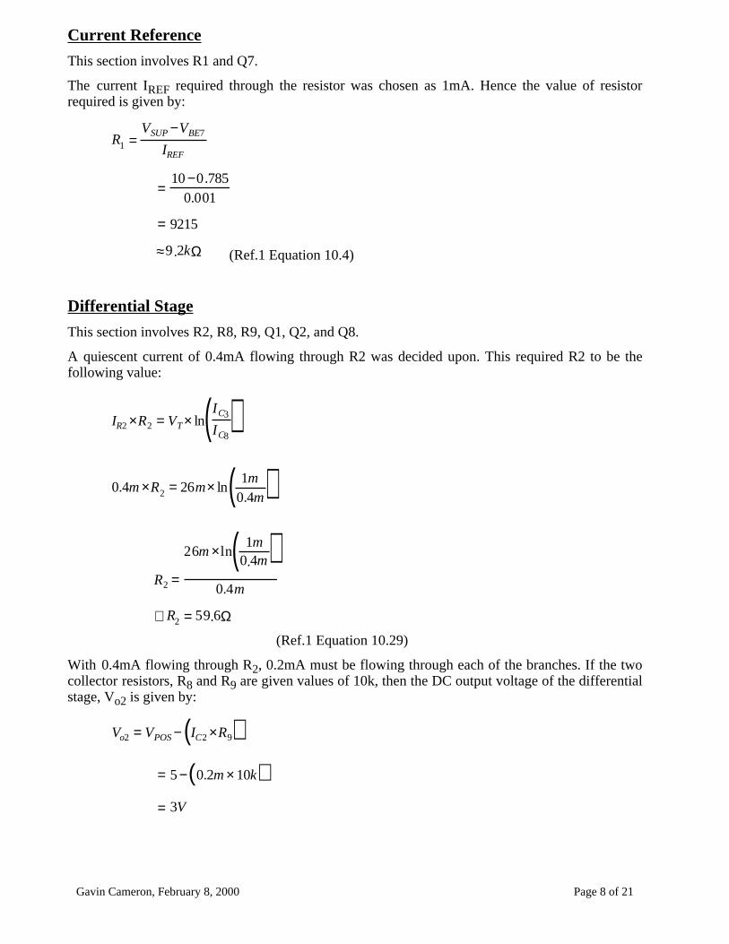
Current Reference
This section involves R1 and Q7.
The current IREF required through the resistor was chosen as 1mA. Hence the value of resistor required is given by:
R1 =VSUP −VBE7
IREF
=10 −0.785
0.001
= 9215
≈9.2kΩ (Ref.1 Equation 10.4)
Differential Stage
This section involves R2, R8, R9, Q1, Q2, and Q8.
A quiescent current of 0.4mA flowing through R2 was decided upon. This required R2 to be the following value:
IR2 ×R2 = VT × ln( )IC3
IC8
0.4m ×R2 = 26m× ln( )1m0.4m
R2 =
26m × ln( )1m0.4m
0.4m
∴R2 = 59.6Ω
(Ref.1 Equation 10.29)
With 0.4mA flowing through R2, 0.2mA must be flowing through each of the branches. If the two collector resistors, R8 and R9 are given values of 10k, then the DC output voltage of the differential stage, Vo2 is given by:
Vo2 = VPOS − ( )IC2 ×R9
= 5 −( )0.2m × 10k
= 3V

Gavin Cameron, February 8, 2000 Page 9 of 21
This limits the common mode input voltage to: − 4.3 ≤ VCM ≤3
Gain Stage
Let IR4 be 0.4mA as well. Therefore, the value of R4 is as follows:
R4 =Vo2 −2( )VBE
0.4m
∴R4 = 4kΩ
For the output of the gain stage to be half way between the supply and the input of the gain stage (V02), V03 must equal 4V, making R5 as follows:
R5 =VPOS −Vo2
IR5
=5 − 40.4m
∴R5 = 2.5kΩ
This will give a symmetrical voltage swing.
Output Stage
Assuming that R3 = R2 = 59.6Ω, then IR6 = IQ = 0.4mA.
Q5 and R6 allow a DC shift, therefore, to drop the voltage VB6 to 0.7V, R6 is:
VB6 = Vo3 − VBE − IR6 × R6
∴R6 =Vo3− VBE −VB6
IR6
= 4 −0.7− 0.70.4m
∴R6 = 6.5kΩ
This will produce 0V output when 0V differential input is applied.
Finally, assume the current through R7 to be 2mA, then R7 is:
R7 =Vo− VNEG
IR7
=0 −( − 5)
2m
∴R7 = 2.5kΩ

Gavin Cameron, February 8, 2000 Page 10 of 21
AC Analysis
The gain of the op-amp can be expressed as:
Ad = Ad1 × A2 × A3
= ( )Vo2
Vin1 − Vin2
×( )Vo3
Vo2
× ( )V0
Vo3
(Ref.1 Example 11.16)
Where Ad1 is the gain of the differential stage, A2 the gain stage and A3 the output stage.
Ad1 = ( )Vo2
Vin1− Vin2
=gm
2 ( )R9/ /Ri2
(Ref.1 Example 11.16)
Where Ri2 is the input resistance of the Darlington pair:
Ri2 = rπ3 +(1 +β)rπ4 (Ref.1 Example 11.16)
Where:
rπ4 =β× VT
IR4
=347 × 26m
0.4m
∴rπ4 = 22.555kΩ
rπ3 =β2 ×VT
IR4
= (347)2 ×26m0.4m
∴rπ3 = 7.827MΩ (Ref.1 Example 11.16)
Therefore:
Ri2 = 7.827M +(1+ 347) +22.555k
∴Ri2 = 15.676MΩ(Ref.1 Example 11.16)
Since R9 >> Ri2, we can ignore Ri2 as it is so high it will not affect the differential stage.

Gavin Cameron, February 8, 2000 Page 11 of 21
gm =IQ
2 × VT
=0.4m
2 ×26m
∴gm = 7.69mS (Ref.1 Example 11.16)
Therefore:
Ad1 =gm
2 ( )R9/ /Ri2
= 7.69m2
×10k
∴Ad1 = 38.45 (Ref.1 Example 11.16)
For the Darlington section (gain stage):
A2 = − ( )IR4
2 × VT( )R5/ /Ri3
(Ref.1 Example 11.16)
Where Ri3 is the input resistance of the output stage:
Ri3 = rπ5 +( )1 +β [ ]R6 + rπ6 + ( )1 + β R7
(Ref.1 Example 11.16)
Where:
rπ5 =β× VT
IR6
=347 × 26m
0.4m
∴rπ5 = 22.555kΩ
rπ6 =β× VT
IR7
=347 × 26m
2m
∴rπ6 = 4511Ω (Ref.1 Example 11.16)
Therefore:
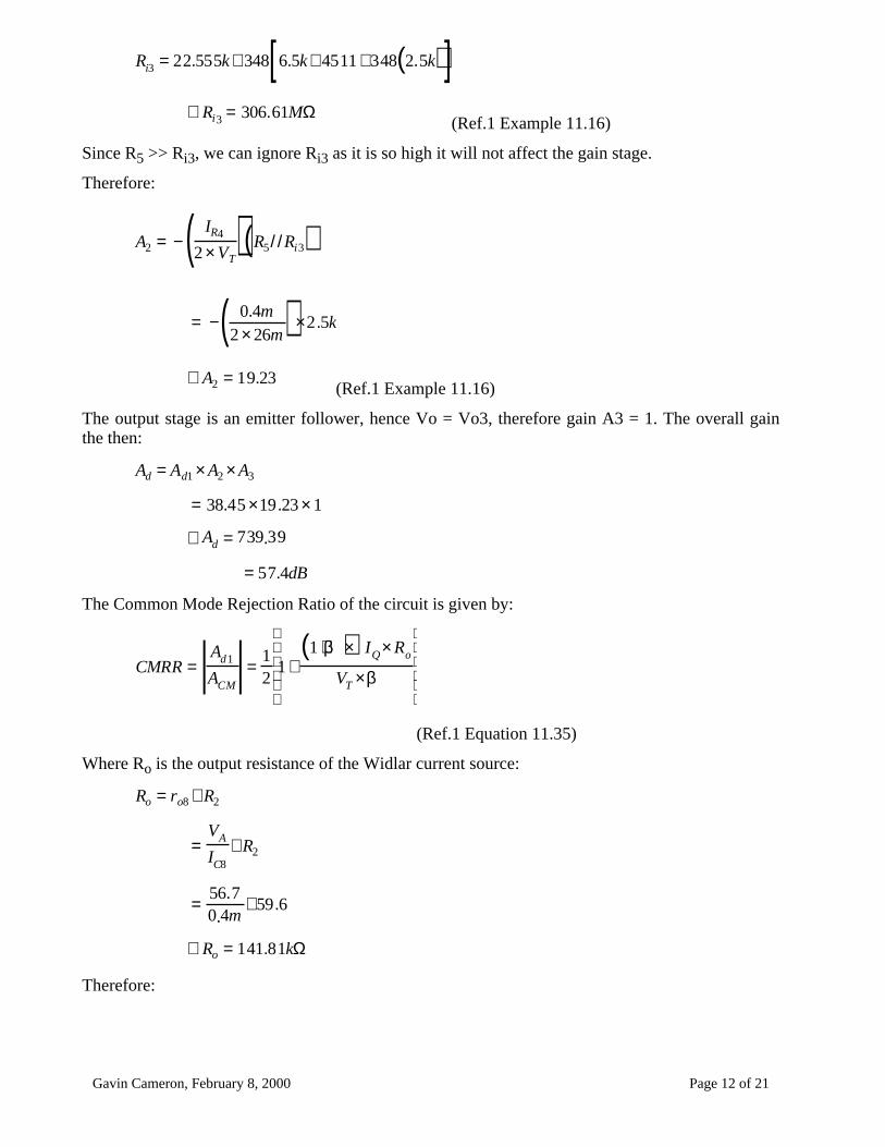
Gavin Cameron, February 8, 2000 Page 12 of 21
Ri3 = 22.555k+ 348[ ]6.5k+ 4511 +348( )2.5k
∴Ri3 = 306.61MΩ(Ref.1 Example 11.16)
Since R5 >> Ri3, we can ignore Ri3 as it is so high it will not affect the gain stage.
Therefore:
A2 = − ( )IR4
2 × VT( )R5/ /Ri3
= −( )0.4m2 × 26m
×2.5k
∴A2 = 19.23(Ref.1 Example 11.16)
The output stage is an emitter follower, hence Vo = Vo3, therefore gain A3 = 1. The overall gain the then:
Ad = Ad1 × A2 × A3
= 38.45 ×19.23 × 1
∴Ad = 739.39
= 57.4dB
The Common Mode Rejection Ratio of the circuit is given by:
CMRR = | |Ad1
ACM
= 12
1 +( )1 + β ×IQ× Ro
VT ×β
(Ref.1 Equation 11.35)
Where Ro is the output resistance of the Widlar current source:
Ro = ro8 + R2
=VA
IC8
+ R2
= 56.70.4m
+59.6
∴Ro = 141.81kΩ
Therefore:

Gavin Cameron, February 8, 2000 Page 13 of 21
CMRR = 12
1 +( )1 +347 ×0.4m ×141.81k
26m ×347
∴CMRR = 1094.5
= 60.8dB

Gavin Cameron, February 8, 2000 Page 14 of 21
ANALYSIS OF CIRCUITThe circuit was analyzed using AIM Spice on a PC. See appendix A for the Spice netlist of the circuit.
Initially, the capacitor C1, was omitted from the design as no hint of capacitor value was given in the design book. Doing this, the circuit did not perform as expected in the gain stage. Applying an AC waveform of 1mV to the Vin1 input while holding Vin2 at 0V, the following was obtained:
Table 2 - Gains of stages
Measured Point AC Voltage Gain of StageVo2 41mV 41Vo3 25mV 0.6Vo 24mV 1 (approx)
Capacitor C1 was added, starting at a nominal 50nF. It was noted that the gain increased at the higher frequencies to the calculated gain. By increasing the capacitor value, the lower cut-off frequency tended to 0. At this point, a capacitor of 47000uF was in the circuit, resulting in a flat response from 0 up to 10kHz.
The DC offset voltages were then examined and found to be approximately the calculated results. Any differences were due to the base-emitter voltage not being exactly calculated, i.e. 0.7V was taken during some calculations. Also, the reference current, IREF is not exactly 1mA due to the rounding error in selecting the resistor value. The offset voltage of the output Vo was -0.15V. This was adjusted by varying the value of R6 from 6.5k to 6.1k. Shown below in figure 2 are all DC voltages in the circuit:
Figure 2 - DC offset voltages

Gavin Cameron, February 8, 2000 Page 15 of 21
As can be seen, the new output offset voltage Vo which is V(14), i.e. node 14, is 1.7mV. The other voltages of importance to note are V(7) which is Vo2 in calculations and V(8) which is Vo3. These are approximately 3V and 4V respectively, as calculated.
The input offset voltage is thus:
VIoff =VOoff
Av=
1.7m1120
= 1.5uV
The input and output AC analysis waveform from each stage are shown below in figures 3 to 5:
Figure 3 - Differential stage
Figure 4 - Gain stage

Gavin Cameron, February 8, 2000 Page 16 of 21
Figure 5 - Output stage
The gains of the various stages are shown below in table 3:
Table 3 - Final gains of stages
Measured Point AC Voltage Gain of StageVo2 38mV 38Vo3 1.17V 30Vo 1.12V 1 (approx)
The overall gain of the amplifier is:
Av =Vout
Vin=
1.121m
= 1120 = 61dB
This is far better than the expected gain of the amplifier which was 739. This is due to the rounding errors performed during the calculations compared to the accuracy of the model used in the spice deck as a full set of spice parameters were used.
The gain-bandwidth product of the amplifier is:
VoMAX = 1.12V
12
power point =VoMAX
2
=1.12
2
= 0.79V
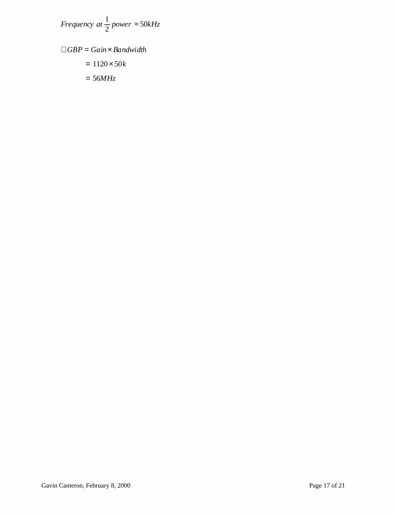
Gavin Cameron, February 8, 2000 Page 17 of 21
Frequency at12
power ≈ 50kHz
∴GBP = Gain × Bandwidth
= 1120 × 50k
= 56MHz

Gavin Cameron, February 8, 2000 Page 18 of 21
CONCLUSIONThe circuit, when simulated, performed much better than expected due to calculation assumptions and approximations.
It met most of the requirements placed upon it. Below is a table of comparison between requirements and achieved results:
Table 3 - Requirements comparison
Parameter Required AchievedVoltage Gain >60dB 61dBGain Bandwidth Product 1MHz 56MHzCommon Mode Rejection Ratio 1% 60.8dBPower Supply +/- 5V +/- 5VOutput Current >100uA 2mAOutput Swing +/- 1V +/- 1.12VInput Offset Voltage < +/- 25uV 1.5uVPower Dissipation < 1mW >1mWSlew Rate > 2V/us <2V/us
The student has learned how important bias currents and DC offsets are in designing a DC coupled amplifier, which without careful calculation, could prevent the circuit from functioning.
During this investigation, the student discovered many configurations of amplifier ranging from the relatively simple design in this report to very complex designs involving active loads and combinations of bi-polar and CMOS technology.
There is still a lot of material on analogue electronics that the student can learn about. This investigation into amplifiers has started the student on his quest into the analogue world.

Gavin Cameron, February 8, 2000 Page 19 of 21
REFERENCES1. Electronic Circuit Analysis and Design, Donald A Neamen, WCB/McGraw-Hill, 1996, ISBN 0071143564.
2. AIM Spice - http://www.eece.napier.ac.uk/~analogue/files/aimspice.exe

Gavin Cameron, February 8, 2000 Page 20 of 21
APPENDIX A - Spice Netlist
Operational Amplifier* Gavin Cameron* MSc/PGD Electronic and Communication Engineering
* Power SupplyVPOS 1 0 DC 5VVNEG 2 0 DC -5V
* Input SignalVIn1 15 0 AC 1m VIn2 16 0 DC 0
* Output StageR3 13 2 59.6Q9 12 3 13 BJTNPNQ5 1 8 11 BJTNPNR6 11 12 6.1kQ6 1 12 14 BJTNPNR7 14 2 2.5k
* Gain StageQ3 8 7 9 BJTNPNQ4 8 9 10 BJTNPNR5 1 8 2.5kR4 10 0 4kC1 10 0 47000u
* Differential StageR2 4 2 56.9Q8 5 3 4 BJTNPNR8 1 6 10kR9 1 7 10kQ1 6 15 5 BJTNPNQ2 7 16 5 BJTNPN
* 1mA Reference Current SourceR1 1 3 9.2KQ7 3 3 2 BJTNPN
* Model for the BC337 transistor.MODEL BJTNPN NPN(IS=4.35e-17 NF=0.853 NR=0.853 RE=0.182 RC=1 VAF=56.7 VAR=28.3+ ISE=287f ISC=287f NE=1.5 NC=1.5 BF=347 BR=5 IKF=0.198 IKF=0.198+ CJC=12.3p CJE=33p VJC=0.273 VJE 0.785 TF=758p TR=98.5n KF=0 AF=1)

Gavin Cameron, February 8, 2000 Page 21 of 21
APPENDIX B - FINAL SCHEMATIC


