Analysis and design of a novel fixed-frequency buck-boost zero-current zero-voltage switched converter G.loannidis E.Xanthoulis S.N.Manias Indexing terms: DC-DC converters, Zero-voltage switching, Soft commutation Abstract: A novel buck-boost ZC-ZVS converter regulated by PWM-control technique is proposed. Soft switching commutation is achieved for all active devices, and consequently the power losses and electromagnetic interference (EMI) arc considerably reduced. The proposed converter can be used for low-EM1 applications using IGBTs or MOSFETs. The principles of operation, theoretical analysis and experimental results are provided to verify the performance of the proposed converter. List of symbols CO = output-filter capacitor C, = resonant capacitor D = buck-boost diode D,,, = diode which is in series with the auxiliary switch Ds = diode which is in series with the main switch ILm = main (buck-boost) inductor current iLr = resonant inductor current L, = main (buck-boost) inductor L, = resonant inductor Po = output power S = main switch Sa, = auxiliary switch T, = switching period vLm = voltage across inductor L, vcr = voltage across resonant capacitor vin = input voltage v, = output voltage 1 Introduction The ever-increasing demand for smaller and more effi- cient DC-DC converters has led to an increase of their operating frequency. Numerous authors have suggested 0 IEE, 1998 IEE Proceedings online no. 19981563 Paper first received 24th January and in revised form 9th July 1997 The authors are with the Department of Electrical & Computer Engineering, Electric Power Division, National Technical University of Athens, 42, 28th October Street, 10682 Athens, Greece resonant topollogies not only to reduce the increased losses due to the high switching frequencies but also to reduce the level of EM1 produced. In some of these cir- cuits [l], frequency modulation is applied to regulate the output voltage, and in others [2-81 the PWM-con- trol technique is used with the introduction of an auxil- iary switch. However, these converters exhibit the following disadvantages when are compared with the conventional one: (a) Converters without auxiliary switch [ 11: (i) higher voltage and current stresses of the semicon- ductor devices; (ii) larger AC energy flow with associated power losses; (iii) variable switching frequency and consequently complex control circuit and filter design are needed; and (iv) poor voltage regulation. (b) Converters with auxiliary switch: (i) the auxiliary switch exhibiting power losses during the turn-off transition [3]; (ii) increased voltage and current stresses of the main and the auxiliary switches 1[4, 5, 81; (iii) auxiliary !switch causing the main switch to have ZC transition only during turn-off [5]. f Fig. 1 Proposed buck-boost ZC-ZVS converter Fig. 1 presents the propos,ed zero-current zero-voltage switched (ZC-ZVS) buck-boost converter which has none of the disadvantages of the conventional resonant converter with an auxiliary switch. The proposed con- verter achieves zero-voltage switching for the main switch and zero-current switching with zero voltage at turn-off for the auxiliary s,witch. Furthermore, there is no reverse-recovery problem for the buck-boost diode since the current through it decreases linearly. There- fore, thanks to the existence of soft commutation for 33 IEE Proc.-Electr. Power Appl., Vol. 145, No. 1, January 1998
Transcript
Analysis and design of a novel fixed-frequency buck-boost zero-current zero-voltage switched converter
Abstract: A novel buck-boost ZC-ZVS converter regulated by PWM-control technique is proposed. Soft switching commutation is achieved for all active devices, and consequently the power losses and electromagnetic interference (EMI) arc considerably reduced. The proposed converter can be used for low-EM1 applications using IGBTs or MOSFETs. The principles of operation, theoretical analysis and experimental results are provided to verify the performance of the proposed converter.
List of symbols
CO = output-filter capacitor C, = resonant capacitor D = buck-boost diode D,,, = diode which is in series with the auxiliary switch Ds = diode which is in series with the main switch ILm = main (buck-boost) inductor current iLr = resonant inductor current L, = main (buck-boost) inductor L, = resonant inductor Po = output power S = main switch Sa, = auxiliary switch T, = switching period vLm = voltage across inductor L, vcr = voltage across resonant capacitor vin = input voltage v, = output voltage
1 Introduction
The ever-increasing demand for smaller and more effi- cient DC-DC converters has led to an increase of their operating frequency. Numerous authors have suggested
0 IEE, 1998 IEE Proceedings online no. 19981563 Paper first received 24th January and in revised form 9th July 1997 The authors are with the Department of Electrical & Computer Engineering, Electric Power Division, National Technical University of Athens, 42, 28th October Street, 10682 Athens, Greece
resonant topollogies not only to reduce the increased losses due to the high switching frequencies but also to reduce the level of EM1 produced. In some of these cir- cuits [l], frequency modulation is applied to regulate the output voltage, and in others [2-81 the PWM-con- trol technique is used with the introduction of an auxil- iary switch. However, these converters exhibit the following disadvantages when are compared with the conventional one: (a) Converters without auxiliary switch [ 11: (i) higher voltage and current stresses of the semicon- ductor devices; (ii) larger AC energy flow with associated power losses; (iii) variable switching frequency and consequently complex control circuit and filter design are needed; and (iv) poor voltage regulation. (b) Converters with auxiliary switch: (i) the auxiliary switch exhibiting power losses during the turn-off transition [3 ] ; (ii) increased voltage and current stresses of the main and the auxiliary switches 1[4, 5, 81; (iii) auxiliary !switch causing the main switch to have ZC transition only during turn-off [5] .
f
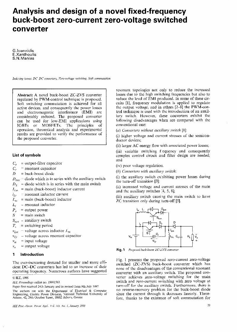
Fig. 1 Proposed buck-boost ZC-ZVS converter
Fig. 1 presents the propos,ed zero-current zero-voltage switched (ZC-ZVS) buck-boost converter which has none of the disadvantages of the conventional resonant converter with an auxiliary switch. The proposed con- verter achieves zero-voltage switching for the main switch and zero-current switching with zero voltage at turn-off for the auxiliary s,witch. Furthermore, there is no reverse-recovery problem for the buck-boost diode since the current through it decreases linearly. There- fore, thanks to the existence of soft commutation for
33 IEE Proc.-Electr. Power Appl., Vol. 145, No. 1, January 1998
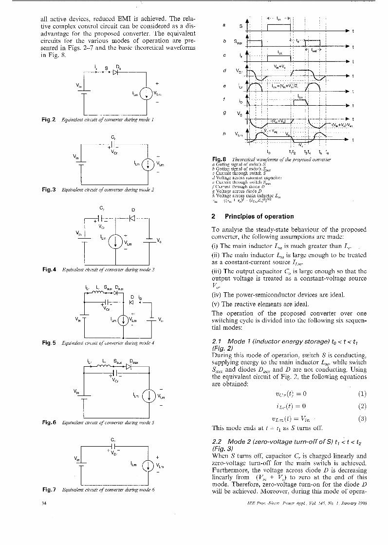
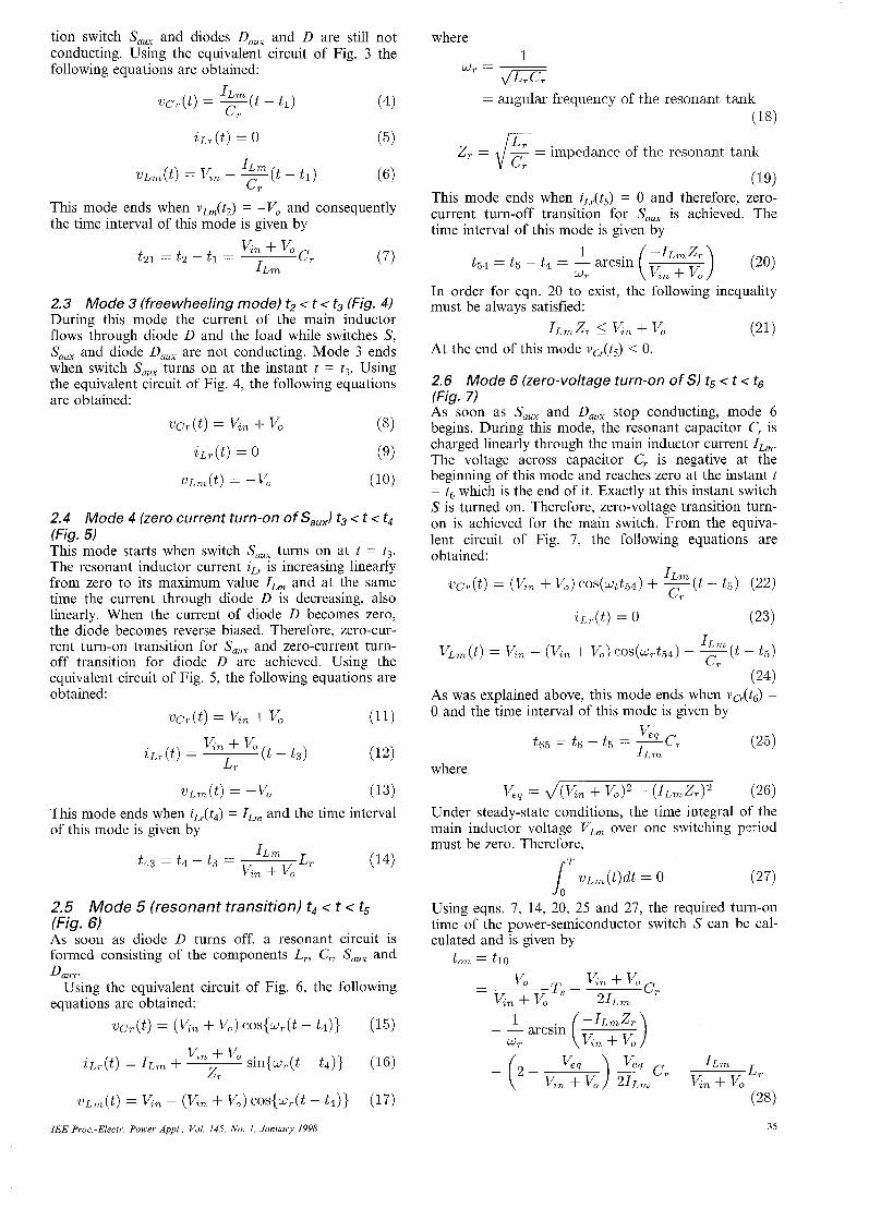
all active devices, reduced EM1 is achieved. The rela- tive complex control circuit can be considered as a dis- advantage for the proposed converter. The equivalent circuits for the various modes of operation are pre- sented in Figs. 2-7 and the basic theoretical waveforms in Fig. 8.
. . . . . . bt
Fig.2 Equivalent circuit of converter during mode 1
Fig.3 Equivalent circuit of converter during mode 2
Cr D
"in FX+---l,, T - . Y' Tvo
Fig. 4 Equivalent circuit of converter during mode 3
1 - I Fig.5 Equivalent circuit of converter during mode 4
U- Fig.6 Equivalent circuit of converter during mode 5
Fig. 7 Equivalent circuit of converter during mode 6
VD
"L,
t0 t l t2 5t4 t, t, Theoretical waveforms of the proposed convertev Fig. 8
a Gating signal of switch S b Gating signal of switch Sa,, c Current through switch S d Voltage across resonant capacitor e Current through switch Sa,, f Current through diode D g Voltage across diode D h Voltage across main inductor L, "eq = {("rn + - (LJr)2}1'2
2 Principles of operation
To analyse the steady-state behaviour of the proposed converter, the following assumptions are made: (i) The main inductor L, is much greater than Lr. (ii) The main inductor L, is large enough to be treated as a constant-current source ILm. (iii) The output capacitor CO is large enough so that the output voltage is treated as a constant-voltage source
(iv) The power-semiconductor devices are ideal. (v) The reactive elements are ideal The operation of the proposed converter over one switching cycle is divided into the following six sequen- tial modes:
Vo.
2. I Mode I (inductor energy storage) to < t < tl (Fig. 2) During this mode of operation, switch S is conducting, supplying energy to the main inductor L,, while switch Sa,, and diodes D,,, and D are not conducting. Using the equivalent circuit of Fig. 2, the following equations are obtained:
w r ( t ) = 0 (1)
Z L T ( t ) = 0 (2)
uLm(t) = Kn (3) This mode ends at t = t l as S turns off.
2.2 Mode 2 (zero-voltage turn-off of S) t l < t < t2 (Fig. 3) When S turns off, capacitor Cr is charged linearly and zero-voltage turn-off for the main switch is achieved. Furthermore, the voltage across diode D is decreasing linearly from -(VLu + Vo) to zero at the end of this mode. Therefore, zero-voltage turn-on for the diode D will be achieved. Moreover, during this mode of opera-
IEE Proc -Electr Power Appl, Vol 145, No 1 January 1998 34
tion switch Sa,, and diodes D,,, and D are still not conducting. Using the equivalent circuit of Fig. 3 the following equations are obtained:
(4)
i L T ( t ) = 0 (5)
ILm CT
vcT(t) = -(t - t l)
(6) 1 L m
CT vLm(t) = v,, - -(t - t l )
This mode ends when vLm(t2) = -Vo and consequently the time interval of this mode is given by
(7) Kn + Vo cT tal = t 2 - tl =
I L m
2.3 Mode 3 (freewheeling mode) t;, < t < t3 (Fig. 4) During this mode the current of the main inductor flows through diode D and the load while switches S, Sa,, and diode D,,, are not conducting. Mode 3 ends when switch Sa,, turns on at the instant t = t3. Using the equivalent circuit of Fig. 4, the following equations are obtained:
~ c T ( t ) = Kn + Vo (8)
iLT( t ) = 0 (9)
vLm(t) = -V, (10)
2.4 Mode 4 (zero current turn-on of Sa,,) t3 < t < t4 (Fig. 5) This mode starts when switch S,,, turns on at t = t3. The resonant inductor current iLr is increasing linearly from zero to its maximum value I,, and at the same time the current through diode D is decreasing, also linearly. When the current of diode D becomes zero, the diode becomes reverse biased. Therefore, zero-cur- rent turn-on transition for S,,, and zero-current turn- off transition for diode D are achieved. Using the equivalent circuit of Fig. 5, the following equations are obtained:
~ c T ( t ) = Kn + Vo (11)
VLm(t) = -K (13) This mode ends when iLr(t4) = ILm and the time interval of this mode is given by
LT I L m
v,n + V o t 4 3 = t 4 - t 3 =
2.5 Mode 5 (resonant transition) t4 c t c t5 (Fig. 6) As soon as diode D turns off, a resonant circuit is formed consisting of the components L,, C,, Sa,, and
Using the equivalent circuit of Fig. 6, the following Dam.
equations are obtained:
vcT(t) (Kn + V o ) cos{wr(t - t 4 ) ) (15)
sin{w,(t - t 4 ) ) (16) v,n + vo ZT
u L m ( t ) = Kn - (Kn + V o ) cos{wT(t - t4) )
i L T ( t ) = ILm +
(17)
IEE Proc.-Elect,. Power Appl., Vol. 145, No. 1, January 1998
where 1
WT = -- dzc
= angular frequency of the resonant tank
ZT = & = impedance of the resonant tank
This mode ends when iLY(t5) = 0 and therefore, zero- current turn-off transition for s,,, is achieved. The time interval of this mode is given by
(18) -
(19)
1 W r
t54 = t:j - t 4 = - arcsin
In order for eqn. 20 to exist, the following inequality must be always satisfied:
At the end of this mode +,(t5) < 0. I L ~ Z T I Kn + Vo (21)
2.6 Mode 6 (zero-voltage turn-on of S) t5 c t < t6 (Fig. 7) As soon as S,,, and D,,, stop conducting, mode 6 begins. During this mode, the resonant capacitor Cr is charged linearly through the main inductor current ILm. The voltage across capacitor C, is negative at the beginning of this mode anld reaches zero at the instant t = t6 which is the end of it. Exactly at this instant switch S is turned on. Therefore, zero-voltage transition turn- on is achieved for the main switch. From the equiva- lent circuit of Fig. 7, ihe following equations are obtained:
vcT(t) ( '6n + VO) coa(wtt54) + -(t ILm - t 5 ) (22) CT
Z L T ( ~ ) = 0 ( 2 3 )
Vi,m(t) = Kn - (Kn + 14) ~os(wTt54) - -(t - t 5 )
(24)
ILm CT
As was explained above, this mode ends when vCu(t6) = 0 and the time interval of this mode is given by
(25)
veq = ~ W F ~ 0 ) ' - ( I L ~ Z T ) ~ (26) Under steady-state conditions, the time integral of the main inductor voltage VI,m over one svitching psriod must be zero. Therefore,
Ve 4 ILm
t 6 5 = t 6 -- t 5 =
where
1' vLm(t)dt = 0 (27)
Using eqns. 7, 14, 20, 25 and 27, the required turn-on time of the power-semiconductor switch S can be cal- culated and is given by
t o n = t l 0
Moreover, using eqns. 7, 14, 20, 26 and 28, the interval time of mode 3 (free-wheeling mode) can be calculated and is given by At = t 3 2
(29) Using eqns. 14 and 20, the required turn-on time of the auxiliary semiconductor switch Sa,, can be calculated and is given by
t o n 2 = t 4 3 + t 5 4
The time delay td between the gating signals of the two semiconductor switches (Fig. 8) is calculated using eqns. 7 and 29 and is given by
t d = t a l + At
Cr
(31)
(32 )
- Kn Kn + Vo cT + V& -
Kn + V o Ts+ 2I,, 2(Kn + V o ) l L m
The average input current of the converter is given by
I,, = I L ~ - I D = IL , - Io where I, is the average current through buck-boost diode and Io is the output current.
Using the assumptions made at the beginning of this Section, the input power of the converter is equal to its output power and consequently the current source I,, is given by
(33 )
atings of the semiconductor devices
The peak voltage and current ratings of the active and passive semiconductors assumed in Figs. 2-8 and eqns. 8 and 16 are
,. I s 1 ID, = I D = I L ~ (34)
The power capabilities of such a converter is limited by the voltage and current ratings of the semiconductors devices, and also by the reduction in efficiency due to the connection of the diodes Ds and D,,, in series with the main switch and the auxiliary switch, respectively. The power range is of the order of several hundreds of watts. This converter would be suitable for applications for which a low level of EM1 is strictly required, such as military applications.
4 Control circuit
The topology of the control circuit and its key wave- forms are shown in Fig. 9. The regulation of the output voltage is achieved by the use of two control loops: an
36
inner current loop and an outer voltage loop. There- fore, current-mode PWM technique [9], adapted for the ZC-ZVS converter, is used.
Fig. 9 Control circuit ofproposed ZC-ZVS buck-boost converter
The voltage of the resonant capacitor vcr is fed to a zero-crossing detector. The output signal CP is a train of pulses with period T, which sets the FIF1 and there- fore, switch S is turned on. The output voltage is fed to an error amplifier and its output is compared with the main inductor current ILm. The output of the compara- tor resets the (FIF1).
The input and output voltage, the main inductor and the signal CP are fed to a microcontroller [8] which outputs two signals, Vtd and ton2. Vtd is a pulse which sets FlF2 (thus switch Sa,, turns on) td seconds after switch S turns on. The time interval td is the time delay between the gating signals of the two switches (Fig. 8) and is calculated using eqn. 31. ton2, as was mentioned in a previous Section, is the time interval for which switch Sa,, is on and is used as an input for the time- delay circuit (Fig. 9) which resets FlF2. The time inter- val ton2 is calculated using eqn. 30. The correct calcula- tion of these signals ensures that the period of the CP signal is constant and equal to T,.
5 Design example
To verify the operation principles of the proposed ZC- ZVS buck-boost converter, the next design example is given: V,, = 48V, Vo = 60V, Po = 1OOW and f, = 20kHz.
The resonant frequency5 = u,l2n is chosen to be 5 = 103.2 kHz Using eqn. 33 and the above specifications, the main inductor current is found to be
Taking into consideration eqn. 21, it is found that
To ensure zero-current turn-off for the auxiliary switch, Z, is chosen to be
Z, = 22.7Q Using eqns. 18 and 19, the following values for the ele- ments of the resonant tank are found:
ILm = 3.15A
Z, 5 28.8Q
Cr = 68nF L, = 35pH
Using eqn. 26 and the above values, the voltage Veq is found to be Veq = 66.5V
IEE Pvoc -Elect, Power Appl , Vol 145, No 1, January 1998
The time intervals for the six modes of operation are calculated using eqns. 7, 14, 20, 25, 28 and 29 and are found to be
Finally, using eqns. 34-38 the peak values for the volt- age and current of the semiconductor devices are calcu- lated: is = fDs = fD = 3.75A
P, = Vsaux = 108V PDs = PDaux = 66.5V Po = 174.5V
5.1 Simulated results The simulated waveforms of interest for this specific design example were obtained using a commonly used software package (SPICE) and are presented in Figs. 10-14. The main and auxiliary switch voltage and cur- rent are presented in Figs. 10 and l l , respectively. The zero-voltage switched for the main switch and the zero- current zero-voltage switched for the auxiliary switch are clearly shown. In Fig. 12 the buck-boost diode volt- age and current are presented, and the soft commuta- tion for this device is also shown. Finally, the voltages across the resonant capacitor and the buck-boost inductor are presented in Figs. 13 and 14. As can be seen, the simulated results are in close agreement with the theoretical ones.
L u x =Afoaux = 8.5.4
8
6
> - i 4
2
0
100
50
> >i 0
-50
-1 00 2.490 2.500 2.510 2.520 2.530
time,ms Fig. 10 1 voltage 2 current
Simulated waveforms ofthe main switch
16 100
12 50
4 -50
0 -100
2.490 2.500 2.510 2.520 2.530 time,ms
Fig. 11 1 voltage 2 current
IEE Proc.-Elects. Power Appl., Vol. 145, No. 1, Januasy 1998
Simulated waveforms of the auxiliary switch
8 0
6 -100
2 -300
0 -400
2.490 2.500 2.510 2.520 2.530 time,ms
Fig. 12 1 voltage 2 current
Simulate(d waveforms of the buck-boost diode
100
50
>
> 6 0
-50
-1 00
2.490 2.500 :2.510 2.520 2.530 time,ms
Fig. 13 Simulated waveform of thle voltage across the resonant capacitor
150
100
VLR 50
0
1 -50
2.490 2.500 2.510 2.520 2.530 time,ms
Fig. 14 tor
Simulated waveform of the voltage across the buck-boost induc-
5.2 Exp e rirn e n ta I res ivlts A lOOW breadboard prototype of the proposed con- verter was built to verify the above analysis and the simulated results. Because of the voltage, current and time requirements, IGT6D21 IGBTs and BYT28 diodes were selected. The experimental waveforms of interest are presented in Figs. 15-19. The main and auxiliary switch voltage and current are presented in Figs. 15 and 116, respectively. In Fig. 17 the buck-boost diode voltage and current are presented. Finally, the voltages across the resonant capacitor and the buck- boost inductor are presenled in Figs. 18 and 19. It is clearly seen that the experimental results are in close agreement with the simulated ones.
31
CHI
Fig. 15 Experimental waveforms of the main switch CH1: voltage across main switch vs (5OV/division, 10pddivision) CH2: main switch current is (2A/division, IOpidivision)
CH2
CH 1
CH2
Fig. 18 Cr (SOVidivision, 1Owidivision)
Experimental waveform of the voltage across resonant capacitor
CHI
CH2
Fig. 17 Experimental waveforms of the buck-boost diode CHI: buck-boost diode voltage vD (5OV/division, IOpidivision) CH2: buck-boost diode current io (2Aidivision, IO~idivision)
6 Conclusions
In this paper a novel fixed-frequency ZC-ZVS buck- boost converter has been analysed and designed. Soft commutation for all active devices is achieved. There- fore, not only the power losses are kept lower than in the conventional hard-switching buck-boost converter but also, and more important, the EM1 is considerably reduced. The theoretical results for the proposed con- verter were confirmed by simulated and experimental results including building a lOOW prototype circuit.
Fig. 19
(SOV/division, IO pidivision)
Experimental waveform of the voltage across buck-boost induc- torL?rI , .
7 References
1 MOHAN, N., UNDELAND, T. and ROBBINS, W.: ‘Power electronics: converters, applications and design’ (J. Wiley & Sons, 1989)
2 HEY, H.L., MATIAS, L., and JUNIOR, J.B.V.: ‘Analysis and design of a buck ZC-ZVS PWM converter’. International sympo- sium on Industrial electronics, ISIE’94, May 1994 HUA, G.C., LEU, C.S., JIANG, Y.M., and LEE, F.L.: ‘Novel zero-voltage-transition PWM converters’. Power Electronics Spe- cialists conference, PESC ’92, Toledo, Spain, July 1992, pp. 55-61
4 HENZE, C.P., MARTIN, H.C., and PARSLEY, D.W.: ‘Zero- voltage switching in high frequency power converters using pulse width modulation’. Applied Power Electronics conference, APEC ’88, 1988, pp. 33-40 MOSCHOPOULOS, G., JAIN, P., and JOOS, G.: ‘A novel zero- voltage switched PWM boost converter’. Power Electronics Spe- cialists conference, PESC ’95, Atlanta, USA, June 1995, pp. 6 9 L 700
6 McMURRAY, W.: ‘Resonant snubbers with active switches’,In- dustrial Application Society conference, IAS’89, 1989,
7 DE DONCKER, R.W., and LYONS, J.P.: ‘The auxiliary quasi- resonant DC link inverter’. Industrial Application Society confer- ence, IAS’90, 1990, pp. 1228-1235 KARVELIS, G.A., and MANIAS, S.N.: ‘Fixed-frequency buck- boost zero-voltage-switched quasiresonant converter’, ZEE Proc. - Electr. Power Appl., 1995, 142, (5), pp. 289-296
9 REDL, R., and SOKAL, N.O.: ‘Current-mode control, five dif- ferent types, used with the three basic classes of power converters: small-signal AC and large-signal DC characterisation, stability requirements and implementation of practical circuits’. Power Electronics Specialists conference, PESC ’85, Toulouse, France, June 1985, pp. 771-785
3
5
8
38 IEE Proc.-Electv. Power Appl., Vol. 145, No. I , January 1998