Page 1
Analysis and Optimization of Monolithic RFDownconversion Receivers
Christopher D. Hull
Electrical Engineering and Computer SciencesUniversity of California at Berkeley
Technical Report No. UCB/EECS-2009-51
http://www.eecs.berkeley.edu/Pubs/TechRpts/2009/EECS-2009-51.html
April 26, 2009
Page 2
Copyright 2009, by the author(s).All rights reserved.
Permission to make digital or hard copies of all or part of this work forpersonal or classroom use is granted without fee provided that copies arenot made or distributed for profit or commercial advantage and that copiesbear this notice and the full citation on the first page. To copy otherwise, torepublish, to post on servers or to redistribute to lists, requires prior specificpermission.
Page 3
Analysis and Optimization of Monolithic RF Downconversion Receivers
by
Christopher D. Hull
B.S. (University of California at San Diego) 1987
M.S. (University of California at Berkeley) 1989
A dissertation submitted in partial satisfaction of the
requirements for the degree of
Doctor of Philosophy
in
Engineering-Electrical Engineering
and Computer Science
in the
GRADUATE DIVISION
of the
UNIVERSITY OF CALIFORNIA at BERKELEY
Committee in charge:
Professor Robert G. Meyer, Chair
Professor Edward A Lee
Professor Heinz O Cordes
1992
Page 4
The dissertation of Christopher D. Hull is approved:
___________________________________________________________
Chair Date
___________________________________________________________
Date
___________________________________________________________
Date
University of California at Berkeley
1992
Page 5
Analysis and Optimization of Monolithic RF Downconversion Receivers
by
Christopher D. Hull
Doctor of Philosophy in
Engineering-Electrical Engineering and Computer Science
University Of California at Berkeley
Professor Robert G. Meyer, Chair
Design considerations for the front-end of radio-frequency receivers are presented.
Emphasis is on silicon bipolar technology for receivers in the 1-3 GHz frequency range,
though theoretical principles derived apply over a broad range of frequencies. Basic
mixer and amplifier topologies are presented and their performance characteristics are
analyzed. Analytic expressions for noise and distortion in linear amplifiers are presented.
The performances of different topologies are compared.
A new method of noise analysis for mixers is presented. The noise analysis is applied to
the emitter-coupled pair mixer over a wide range of parameters variation to allow the
designer to understand how noise performance changes with parameter variations.
Results of distortion simulations over a range of parameters values are also presented.
The mechanisms that create the distortion are explained, and the simulations results are
presented in a way that allows an intuitive link between the simulated value of the
distortion and the mechanism that creates that distortion.
For verification of the methodology presented, the analysis techniques are applied to a
specific circuit and compared to measured values. Computed values are close to the
measured ones.
Abstract Approved: _______________________________
Thesis Chairman
Page 6
Chapter 1: Introduction
Wireless communication is a convenient way to transmit voice or data from point to point, and is
essential for mobile communications. Commercial applications include cellular telephony, global-
positioning satellite, direct-broadcast satellite, and wireless computing. A block diagram of a radio-
frequency transceiver structure used for wireless communication is shown in Figure 1.
LNA MIXING DETECTIONBASEBAND
SIGNAL
PROCESSING
POWER
AMP MODULATION
DATA OUT
DATA IN
Figure 1: Low-Power Transceiver Architecture
The modulator and power amplifier blocks form the transmitter. The LNA (low-noise amplifier),
mixer, detection circuitry, and baseband signal processor form the receiver. The receiver front-end consists
of the LNA and mixing blocks. The purpose of these blocks is to amplify the weak signal received from the
antenna and convert the carrier frequency down to a range that is more easily processed. Detection and
baseband signal processing techniques are dependent on the type of transmission modulation (e.g.
AM,FM,QPSK). The front-end of the receiver will be the focus of this dissertation.
1.1: System Requirements for Commercial RF Receivers
Among the important design considerations are power consumption, cost, physical size, reliability,
selectivity and dynamic range. Selectivity is the ability of a receiver to select the desired signal and reject
the unwanted signals. Dynamic range is the ratio of the maximum signal level the receiver can tolerate with
an acceptable level of distortion over the minimum signal level before noise makes detection impossible.
Page 7
In addressing the design considerations, one must consider the technologies available. Current
technology choices are monolithic circuits vs. discrete circuits, silicon vs. gallium-arsenide, and bipolar
junction transistors vs. field-effect transistors.
Monolithic technology offers the advantages of compact size, higher reliability, and lower
assembly costs. However, discrete designs are easier to adjust. Monolithic implementations involve
considerable start-up costs, and thus are appropriate for high-volume commercial applications. Discrete
implementations are more appropriate for custom design. It should be noted that most systems use a
combination of discrete and monolithic elements.
While GaAs technology offers state-of-the-art performance and is widely used for military
applications, its high cost and low yield make it appropriate where performance is of paramount
importance. The relatively low cost and high yield of silicon technology make large scale integration
practical. This gives silicon a substantial advantage for high-volume commercial applications.
In silicon technology, bipolar transistors offer higher performance than FET devices. While FETs
have comparable device gain-bandwidth products ( Tf ), they require substantially higher gate-source
operating voltages than the base-emitter operating voltage of a bipolar transistor. Associated with this is a
much lower transconductance-to-current ratio. For low-power applications (both low current and low
voltage) the BJT offers considerably better performance. An alternative for FETs is to operate them at low
gate-source voltages. While use of low gate-source voltages improves the transconductance-to-current ratio,
the high-frequency current gain and Tf drop considerably, and the parasitic capacitances become quite
large. As FET sizes scale down, FETs may become practical alternatives to bipolar transistors in the low
GHz range. However, in the current 0.8 micron technology, the performance of FETs suffers drastically
beyond a few hundred MHz. One of the major advantages of FET technology is the ability to integrate with
CMOS digital circuitry. However, with the advent of BiCMOS technology, it is not necessary to sacrifice
performance for integration. It should be noted that PMOS transistors give far better performance than the
parasitic PNPs available in many bipolar and BiCMOS processes. These may be quite useful for active
loads and biasing.
Page 8
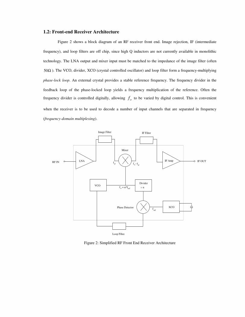
1.2: Front-end Receiver Architecture
Figure 2 shows a block diagram of an RF receiver front end. Image rejection, IF (intermediate
frequency), and loop filters are off chip, since high Q inductors are not currently available in monolithic
technology. The LNA output and mixer input must be matched to the impedance of the image filter (often
Ω50 ). The VCO, divider, XCO (crystal controlled oscillator) and loop filter form a frequency-multiplying
phase-lock loop. An external crystal provides a stable reference frequency. The frequency divider in the
feedback loop of the phase-locked loop yields a frequency multiplication of the reference. Often the
frequency divider is controlled digitally, allowing of to be varied by digital control. This is convenient
when the receiver is to be used to decode a number of input channels that are separated in frequency
(frequency-domain multiplexing).
LNA
XCO
VCODivider
IF Amp
Mixer
Phase Detector
Loop Filter
Image Filter IF Filter
RF IN IF OUT
fref
fo = n*fref
frf fo
- frf
_ n..
Figure 2: Simplified RF Front End Receiver Architecture
Page 9
Chapter 2: Circuit topology for RF Amplifiers and Mixers
LNA
Mixer
Image Filter IF Filter
RF IN IF OUTf
rf fo- f
rf
fo
Input Filter
LO IN
Figure 1: RF Amplifier and Mixer
Figure 1 shows the arrangement of the RF amplifier and the mixer, which together with the local
oscillator, form the front end of the receiver. An input filter is necessary to prevent overload of the LNA
from out of band signals coming from the antenna, and also improves image rejection. Since the amplifier
and mixer take their inputs and outputs from off chip, they must have matched impedances at both the
inputs and the outputs. Impedance matching networks may be used for this purpose. If an image-rejection
mixer is used, then use of an image filter between the preamp and mixer is unnecessary, and hence, the
output impedance of the LNA and input impedance of the mixer need not be matched. Image-rejection
mixers require twice the hardware and power consumption of an equivalent mixer that does not reject the
image frequency. Thus there is a tradeoff between the advantage gained from the increased level of
integration of an image-rejection mixer and the increased power consumption.
2.1: Low-Noise Amplifier Configurations
Of the three basic configurations (common-emitter, common-base, and common collector), the
common-emitter (or common-source for FETs) is the only one offering both current and voltage gain. This
is quite advantageous for noise purposes. Hence, the first stage of any low noise amplifier is almost always
a common-emitter. At high frequencies the common-emitter has a low input and output impedance making
it suitable for matching to the lower impedances typically seen in RF filter systems, cables, and antennas.
Page 10
Common-base stages offer low input impedances, but very high output impedances, and a matching network
is necessary at the output of a common-base stage. Shunt feedback may also be used to reduce the output
impedance, but has limited applicability at high frequencies, as the excess open-loop gain required to give
adequate loop gain is not readily available. Multiple stages may be used to obtain the required loop gain,
but stability issues generally limit the number of stages to two or three. Common-collector stages are
commonly used at low frequencies; however, at high frequencies, the output impedance is quite inductive
and the configuration is prone to parasitic oscillations. For these reasons, common-emitter amplifiers are
preferred for high-frequency matched impedance applications that are narrow-band.
A typical two stage configuration is depicted in Figure 2. Matching networks should be made of
reactive elements to avoid adding additional noise sources to the circuit. In particular, "brute force"
matching with series or shunt resistors should be avoided, as this degrades the noise performance of the
amplifier substantially. The bias network uses negative feedback to stabilize the dc operating point of the
transistors.
+- V
s
VCC
Q1Rs
Matching Network
Matching Network
Input
Output
Q2
Bias Feedback
Circuit
TO IF FILTER
Figure 2: Two-stage low-noise amplifier
Page 11
+
-Vs
Rs
Rf1Re1
RL
Vin
+
-
Rf2
Re2
Q Q
Rcc
Vcc
1 2
VL
+
-
Figure 3: Wideband Matched-Impedance Amplifier
An alternative matching technique is to use feedback. An example of this circuit is shown in Figure
3. The advantage of this technique is that matching occurs over a wide range of frequencies. This is
desirable for general purpose amplifiers. However, feedback amplifiers generally have poorer noise
(especially at high frequencies) compared to non-feedback amplifiers. This dissertation will focus on
topologies that do not use feedback.
2.2: Mixer Configurations
A wide variety of mixer configurations are possible. Fundamentally, all mixers rely on periodic
switching of the signal for down conversion. This is shown schematically in Figure 4.
RF INIF Out
LO SWITCH
+
-
Figure 4: Fundamental Down Conversion Process
Page 12
LO IN
IF OUT
Q Q2 3
+ -
+
-
IQ
IRF
Figure 5: Emitter-Coupled Pair Mixer
In bipolar technology the switch is usually implemented using an emitter-coupled pair as shown in
Figure 5. Note that an input signal in the form of a current is required. This implies that the switch should
be driven with a high source impedance. Since the impedance looking back into the IF filter tends to be low,
a voltage to current conversion stage is necessary. These stages must be matched at the input and have a
high output impedance. Of the three basic circuit configurations, both the common-base and the common-
emitter have the desired properties.
Figure 6 shows a common-base driver for the emitter-coupled pair mixer. Resistor mR matches
the circuit and linearizes the circuit, but also increases the noise of the circuit. In addition, the common-base
stage lacks current gain and thus the current noise from the emitter-coupled pair mixer is referred back to
the input without reduction. An alternative is to use an active matching network at the input. This will
increase the current gain and reduce the noise, but the distortion will also increase.
The common-emitter configuration in Figure 7 has the advantage of better noise performance and
higher gain than the common-base. At low frequencies the linearity is quite poor. However, in the GHz
Page 13
range, the linearity of a well designed common-emitter amplifier may be quite good (see Chapter 3). Stable
biasing is obtained by generating a reference BEV using a diode.
+-
BIAS
Vs
50
Q1
IQ
+ IRF
Rm
Rbias
Figure 6: Common-Base Driver
+- V
s
50 Q
1
IQ
+ IRF
Matching Network
Bias Network
VBE (ref)
Figure 7: Common-Emitter Driver
Page 14
Q
Q
Re2
R f
Cf
RL
V
Vout
1
2
CC
+- V
s
50
IQ
+ IRF
Re1
Figure 8: Current-Feedback Pair Driver
As with preamps, the driver stage of a mixer may use feedback to generate matching over a wide
range of frequencies. The current-feedback pair configuration shown in Figure 8 gives a controlled low-
impedance at the input and a high impedance at the output. The noise performance penalty is minimal.
However, the two stages give somewhat higher gain than desired and consume additional power. Increasing
the degeneration resistor, 1eR , to reduce the gain will degrade the noise performance.
While FET mixers may be built using circuits directly analogous to the bipolar circuits presented
above, an alternative exists for FETs that does not exist for bipolar transistors. With bipolar transistors, if
the collector-emitter potential is dropped below about 0.2V, the collector-base junction becomes forward
biased, and the base is flooded with charge (saturation). It takes a substantial amount of time for the
transistor to recover from this condition. However, FETs do not exhibit this behavior. Thus, a FET can be
switched on and off by changing its drain-source potential. A simple circuit configuration that achieves this
is shown in Figure 9. The gate of 2J is controlled by the LO, and this in turn controls the drain-source
potential of 1J . This configuration is very advantageous since the drain region of 1J and the source region
of 2J may be combined into a single region. No external contact to this region is necessary. This decreases
Page 15
the parasitic capacitance associated with that node of the circuit. When these region areas are combined a
new four terminal device known as a dual-gate FET is formed. Dual-gate FET mixers are frequently used in
GaAs technology.
+
-Vs
R s
VLO
IF OUT
Matching Network
J
J
1
2
Figure 9: Complete dual-gate FET Mixer
2.3: Double-Balanced Mixers
All of the above mixers are either single-balanced or unbalanced. A single-balanced mixer allows
either the RF or LO signal to pass to the output with little attenuation. A double-balanced mixer rejects both
the RF and LO frequencies at the output. The fundamental configuration of a double-balance mixer is
shown in Figure 10. The RF, LO, and IF ports all have balanced signals. The two switches operate in
opposite polarity.
IF Out
LO SWITCH
+
RF IN
-
+
-
Figure 10: Fundamental configuration of a double-balanced mixer
Page 16
Figure 11 shows an implementation of the double-balanced mixer using three emitter-coupled
pairs. Two emitter-coupled pairs ( 63 QQ − ) are used to do the switching and one ( 1Q - 2Q ) is used for
voltage to current conversion. The voltage to current driver is degenerated to improve its linearity. This
mixer is often incorrectly referred to as a "Gilbert Cell Mixer". The Gilbert Cell adds pre-distortion
techniques to achieve linear multiplication of the two input signal whereas the circuit in Figure 11 is non-
linear with respect to the LO input. While analog multiplication reduces spurious output signals, the noise
performance of a Gilbert Cell analog multiplier is poorer. Henceforth, the double-balanced emitter coupled
pair mixer without pre-distortion will be referred to as the "Quad" mixer (since four transistors are used to
perform the switching operation).
The inputs to the mixer in Figure 11 are not matched, and a matching network is required. Often
"brute force" matching is used in the form of a resistor to ground. This is disadvantageous from the point of
view of noise performance, but it is often the simplest way to match the RF and LO input ports.
VCC
Q Q
Q1
3 4Q Q
5 6
IQ
Q2
Vout
Vrf
+
-
VLO +
VLO
VLO
+
-
Re Re
Figure 11: Double-Balanced ECP Mixer
Page 17
2.4: Image-Rejection Mixers
While double-balanced mixers prevent RF and LO signals from reaching the output, spurious
signals still exist. Even a mixer which performs ideal multiplication allows two different frequencies to be
converted to the intermediate-frequency. For example, if the LO frequency is 1GHz, the input frequency is
900MHz, and the intermediate-frequency is 100MHz, then signals at 1.1GHz will also be converted down
to the intermediate-frequency. This extra frequency that is converted down to the IF is known as the image
frequency. In most mixer designs, the image frequency is filtered out with a sharp bandpass filter centered
around the signal frequency. However, a combination of two mixers and two 90 degree phase shifters can
be combined to form a mixer that rejects images. A block diagram of an image-rejection mixer is shown in
Figure 12.
RF IN
90 degree
phase shifter
90 degree
phase shifter
LO IN
Σ IF OUT
Figure 12: Image-Rejection Mixer
Page 18
Chapter 3: Low-Noise Amplifiers
Random noise is generated by all resistors and active devices within a circuit. The dominant
mechanisms are random thermal noise in resistors, and shot noise through p-n junctions.
Ideal reactive elements do not generate noise, though they may affect the overall noise
performance in a circuit. Ideal feedback does not add noise; however, resistive feedback does add
additional noise sources. For this reason, resistive feedback is to be avoided in low-noise amplifiers. Since
feedback is commonly used to reduce distortion in amplifiers, designing without feedback requires that
attention be paid to linearity issues. Careful design is required to obtain low noise and acceptable linearity.
Resistive feedback is also commonly used to stabilize the gain and terminal impedances over wide
bandwidths; however, for low noise it is necessary to use other techniques. Reactive impedance matching
networks or reactive feedback may be used to obtain matching over narrow bandwidths. Generally, these
techniques will not achieve a wideband match, and it is therefore necessary to have a specific frequency
range in mind when designing low-noise amplifiers.
3.1: Noise Figure in Amplifiers
The most common measure of noise performance is the noise figure of an amplifier. The noise
figure is defined asi:
out
in
NS
NSF
)/(
)/(= (1)
S/N is the signal-to-noise ratio. The noise figure is thus a measure of the amount by which the signal-to-
noise ratio is degraded. A noise figure of unity (or 0 dB) indicates a noiseless amplifier.
When two amplifiers are cascaded, the overall noise figure is given by:
1
21
111
G
FFF
−+−=− (2)
1G is the power gain of the first stage.
The noise figure of an amplifier is given in terms of its equivalent input voltage and current noise
by:
Page 19
2
2
1
s
snn
v
ZivF
⋅++= (3)
where fRTKv ss ∆⋅⋅⋅⋅= 42
Equation (3) is quite general, and includes the effect of correlation between voltage and current noise at the
input.
3.2: Physical Noise Sources
Bipolar and FET transistors have similar small signal models at high frequencies. The small-signal
model with noise sources included is shown in Figure 1. Ideal feedback does not affect the equivalent input
noise generatorsii; hence, feedback from jcC does not affect the noise figure. However, the loading of jcC
at the input does affect the noise figure somewhat. A good first order approximation for noise calculations is
to add the value of jcC to jeC .
Cπ
rb
(s) * Ib
β( Ib
Cjc
C
E
B
ibn
icn
vbn
+
Figure 1: Transistor Model Including Noise Sources
The variances of the noise sources for bipolar transistors are given byiii
:
frTKv bbn ∆⋅⋅⋅⋅= 42
(4a)
fg
TKi mcn ∆⋅⋅⋅⋅=
24
2 (4b)
o
cn
o
mbn
if
gTKi
ββ
22
24 =∆⋅
⋅⋅⋅⋅= (4c)
For FETs, the variances of the noise sources are:
Page 20
frTKv gbn ∆⋅⋅⋅⋅= 42
(5a)
fgTKi mcn ∆⋅⋅⋅⋅⋅=3
24
2 (5b)
0≈bni (5c)
The equivalent input noise sources are expressed in terms of the three physical noise sources as:
m
cnbnbbn
b
m
cnbnng
ivri
j
r
givv +≈⋅+
⋅++=
)(
1
ωβ (6a)
)( ωβ ⋅
+=j
iii cn
bnn (6b)
For bipolar transistors, all three noise sources play a significant role; however, for FETs, cni dominates.
Flicker noise has been neglected in Equations 4-6 since it is rarely a factor at RF and microwave
frequencies; however, below 100MHz GaAs MESFETs exhibit significant flicker noise.
3.3: Noise Figure in a Single Stage Amplifier
Equations 3 and 6 may be combined to determine the noise figure of a single stage amplifier in
terms of physical noise sources and source impedance. The noise figure is:
2
22
2
22
)(
1
1s
bsbnbs
m
cnbn
v
rZij
rZ
giv
F
+⋅+⋅
++⋅+
+=ωβ
(7a)
If the complex source impedance is written Sss XjRZ ⋅+= , and terms that are on the order of 2
/1 oβ
are neglected, then the noise figure is given by:
[ ]
2
22
22222
)()(
1)(
1S
bSS
m
cnSbsbnbn
v
j
rR
j
X
giXrRiv
F
⋅
++
⋅−⋅+++⋅+
+≈ωβωβ
(7b)
Page 21
The relation: ocnbn ii β/22
= is true for FETs (as well as BJTs) if one interprets ∞→= GDo II /β for
FETs. Therefore, Equation 7b may be written:
2
2222
22 )(
)()(
1
1S
o
SbsbSS
m
cnbn
v
XrR
j
rR
j
X
giv
F
+++
⋅
++
⋅−⋅+
+≈βωβωβ
(7c)
By differentiating Equation 7c , the optimum value for source impedance may be derived. Using
the relationship )/()( inm Cgj ⋅=⋅ ωωβ , the optimum source resistance is given by:
1
222
222
)(
1121−
−
⋅+⋅
⋅⋅⋅−+++=
ωββ
ω
jg
XC
i
vXrR
om
sin
cn
bnsbopts
(8)
The optimum source reactance is:
o
in
o
m
opts
jCjg
jX
β
ωβω
β
ωβ
ωβ22
)(1
11
)(1
1)(
⋅+
⋅⋅
=⋅
+
⋅⋅
=− (9)
In the case that oj βωβ <<⋅ )( , Equation 9 indicates that source reactance is such that it cancels the
input reactance. For FETs the optimal source reactance is always equal and opposite to the input reactance.
Often it is convenient to realize the source reactance, SX , with an inductor. The optimal value of
this inductance is then given by:
oin
min
opts
C
gC
L
βω
⋅+⋅
=− 2
2
1 (10)
3.4: Noise Figure For Bipolar Transistors:
Using Equation 7c and Equations 4a-c, the noise figure of a single-stage BJT amplifier becomes:
Page 22
[ ]( ) [ ][ ]22
22
)(12
1
2
)(1 bSinSin
smso
Sbsm
s
b rRCXCRgR
XrRg
R
rF +⋅⋅+⋅⋅−⋅
⋅⋅+
⋅⋅
++++= ωω
β (11)
The optimum source resistance and transconductance are given by:
1
22
22
)(
11212
−
−
⋅+⋅
⋅⋅⋅−+⋅++=
ωββ
ω
jg
XC
g
rXrR
om
sin
m
bSbopts
(12)
[ ]
o
f
bsjesje
Sbs
optm
rRCXC
XrRg
βτω
ωω
1)(
)()1(
)(
1
2
22
22
+⋅
+⋅⋅+⋅⋅−⋅
++=−
(13)
To obtain the optimum noise performance, Equations 12 and 13 must be solved simultaneously.
Since an analytic solution does not exist, iteration or some other numerical technique must be applied. An
analytic solution exists for ∞→oβ . In that case:
in
optsC
X⋅
→−ω
1 (14a)
[ ]
sm
bSin
s
bopts
Rg
rRC
R
rXF
⋅⋅
+⋅⋅++→−
2
)(1)(
2ω
(14b)
2
)(2
1 ωβ ⋅⋅⋅
+⋅→− jrg
rRbm
bopts (14c)
f
je
optm
Cg
τ→− (14d)
⋅⋅⋅⋅⋅++⋅⋅⋅⋅⋅⋅+→
)()(2
111)()(41
fjeb
fjeboptCr
CrFτωω
τωω (14e)
When
o
To
ffj
ββωβ >>⇔<<⋅
2)( the limiting values given by Equations 14a-e are
close to the exact solution of Equations 12 and 13. Equations 14a-d make a good starting "guess" for
numerical optimization of the noise performance.
Page 23
3.5: Low-Noise Amplifier Realization
+- V
s
VCC
Q1Rs
Matching Network
Output
Bias Feedback
Circuit
TO IF FILTER
Lb
Le
Figure 2: Single-Stage Common-Emitter Amplifier
A low-noise common-emitter amplifier is shown in Figure 2. Input matching is achieved through
the use of package bond-wire inductances. Output matching may be achieved either through an external
matching network or with capacitive shunt feedback.
If the collector-base junction capacitance is neglected, then the input impedance is given by:
sC
sLLLrg
sLsrsZ ebTeb
m
ebin⋅
+⋅++⋅+≈
+⋅⋅+=
π
ωβ1
)(1
)()(
Thus Le gives a resistive component to the input impedance without adding noise. This allows for low-
noise design, while maintaining good matching at the input. The value of emitter bond-wire inductance
required for matching is given by:
tbse rRL τ⋅−= )( (15)
where:
Tm
je
ftg
C
ωττ
1=+=
For noise analysis purposes, the base and emitter bond-wire inductances contribute to the source
reactance. Using Equation 11, the noise figure of this amplifier is:
Page 24
[ ] [ ]22222222 )()1(2
1)(
21 bS
Sm
bs
so
m
s
b rRCCLRg
LrRR
g
R
rF +⋅⋅+⋅⋅−
⋅⋅+⋅++
⋅⋅++= ππ ωωω
β (16)
eb LLL +=
The optimum total inductance is given by Equation 10. While Equation 12 and 13 may be used for
design optimization, quite often it is easier to minimize the noise figure through direct use of an
optimization package. In addition, it is often more convenient to keep the source resistance constant and
allow the device area to vary. The effect of device area on current is manifested through br and jeC .
Consider a process with minimum size devices having parameters: bob rr = and jeoje CC = . Then a
device of area A relative to the minimum size device has:
A
rr bob =
ACgC jeofm ⋅+⋅= τπ
Equation 16 is then minimized with respect to A and cI . To get a starting value for the optimization,
consider the case where ∞→oβ . Equation 14a-d can be transformed to yield:
fjeobos
boopt
CrR
rA
τω ⋅⋅⋅⋅+⋅≈
22
11 (17)
T
f
jeo
optc VAC
I ⋅⋅
≈−τ
(18)
The first order effect of finite oβ may be taken into account via the approximation:
)(
11
1
foo
T
f
jeo
optc VAC
I
τωβ
τ
⋅+
⋅⋅⋅
≈− (19)
Equations 17 and 19 usually give values quite close to the actual optimums. Since the noise figure
is not very sensitive to these parameters, it may be sufficient to use the values obtained from Equations 17
and 19 for an actual design.
Page 25
3.6: Distortion in Single-Stage Amplifiers At High Frequencies:
Volterra Series techniques will be applied to the common-emitter/common-base stage to determine
distortion characteristics. In particular, the third-order intermodulation distortion intercept is accurately
predicted using Volterra techniques. Consider the amplifier configuration shown in Figure 3.
+- V
s
VCC
Q1
Ze
Zb
IQ
Figure 3: Common Emitter/Common-Base Amplifier Configuration
In a Volterra Series, the collector current is expressed in terms of the source voltage as:
3
3213
2
21211 ),,(),()( sssc vavavai ooo ωωωωωω ++=
where the operator o indicates that the amplitude and phase of all sinusoids in n
sv are to be modified by
the magnitude and phase of ),...,,( 21 nna ωωω .
If the collector-base junction capacitance is neglected, then Volterra Series analysis gives:
⋅+⋅⋅⋅⋅++⋅
=
Q
Tje
fbe
Q
Te
I
VCjjZ
I
VjZ
a
τωωω
ω
111
11
)()(
1)( (20a)
Page 26
[ ][ ]2
21212112111
2122
))(1)()()(),(
Q
jebeT
I
CjjZVaaaa
⋅
⋅+(⋅⋅+⋅+⋅⋅+⋅⋅=
ωωωωωωωωωω (20b)
[ ] [ ]33121112113213
3
)(1)()()(3)(),,(
Q
jeoobeT
QoI
CjjZVaaaaaIaa
⋅
⋅⋅⋅⋅+⋅⋅⋅⋅−⋅⋅⋅⋅=
ωωωωωωωωω (20c)
where: )()()( ωωω ⋅+⋅=⋅ jZjZjZ ebbe
321 ωωωω ++=o
3
),()(),()(),()( 21231132213221121
ωωωωωωωωω aaaaaaaa
⋅+⋅+⋅=⋅
Distortion is measured in terms of the ratio of the spurious signal generated and the desired signal
at the output. Spurious signals generated at the output are proportional to:
3213213 ),,( sss vvva ⋅⋅⋅ωωω ,
where vsi is the input amplitude of the i'th input signal. The desired output signal is given by
sso vjai ⋅⋅= )(1 ω . Therefore:
s
sss
s v
vvv
a
aDistortion 321
1
32133
)(
),,( ⋅⋅⋅∝
ω
ωωω
Consider the case where sωω =3 and ss vv =3 . That is, one of the three input signals producing the
distortion also produces the desired output signal.
21
1
2133
)(
),,(ss
s
s vva
aDistortion ⋅⋅∝
ω
ωωω
In this case the distortion is proportional to the signal strength of the two undesired signals.
Now consider the case where all three signals generate outputs that are desired. The output signal
levels for the three desired (non-spurious) signals are:
1111 )( so vai ⋅= ω
2212 )( so vai ⋅= ω
3313 )( so vai ⋅= ω
The conventional way to measure intermodulation distortion is with equal output amplitudes:
oooo iiii === 321
Page 27
In this case:
2
312111
32133
)()()(
),,(oi
aaa
aDistortion ⋅
⋅⋅∝
ωωω
ωωω
Using Equation 20a-c, it is found that:
−
⋅+⋅+⋅+⋅+⋅+⋅⋅
⋅
⋅=
⋅⋅1
2
)()()(
3
)(
)()()(
),,( 133221
2
312111
3213 ωωκωωκωωκωκ
ωωω
ωωω jjjjjj
I
j
aaa
a
Q
o
where
Q
T
Q
Tje
fbe
Q
Te
beje
I
V
I
VCjjZ
I
VjZ
jZCjj ⋅
⋅+⋅⋅⋅⋅++⋅
⋅⋅⋅⋅+≡⋅
τωωω
ωωωκ
)()(
)(1)(
Third order intermodulation distortion is defined as the distortion generated by the cubic non-
linearity with two input signals. Of these signals, often the most important one is the one with output
frequency given by 212 ωωω −⋅=o . For 121 ωωωω <<−≡∆ , the distortion's output frequency is
near the two signal frequencies.
For a constant output level for two input frequencies, the third-order difference intermodulation-
distortion is given by:
2
211
2
1
2113213
)()(
),,(
4
3),( oi
aa
aDIM ⋅
−⋅
−⋅=
ωω
ωωωωω
2
121213 )2(2
1)(1)(
4
1),(
⋅⋅⋅⋅−⋅−⋅−⋅⋅⋅=
Q
oo
I
ijjjjDIM ωκωωκωκωω (21)
The usual situation of interest is when 112 , ωωωωω <<∆∆−≈ . The distortion frequency is
ωωω ∆+= 1o , which often falls in the signal bandwidth, and cannot be filtered out.
The distortion for this case is given by:
2
1213 )2(2
1)(1)(
4
1),(
⋅⋅⋅⋅−∆⋅−⋅⋅⋅≈
Q
oo
I
ijjjDIM ωκωκωκωω (22)
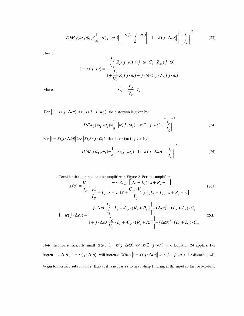
Using the triangle inequality, an upper bound on the distortion can be placed:
Page 28
2
1213 )(1
2
)2()(
4
1),(
⋅
∆⋅−+
⋅⋅⋅⋅⋅≤
Q
oo
I
ij
jjDIM ωκ
ωκωκωω (23)
Now :
)()(1
)()(
)(1
ωωω
ωωω
ωκ
π ⋅⋅⋅⋅+⋅+
⋅⋅⋅⋅+⋅
=⋅−
jZCjjZV
I
jZCjjZV
I
j
bee
T
Q
bebe
T
Q
where: f
T
Q
bV
IC τ⋅=
For )2()(1 1ωκωκ ⋅⋅<<∆⋅− jj the distortion is given by:
2
1213 )2()(8
1),(
⋅⋅⋅⋅⋅⋅≈
Q
oo
I
ijjDIM ωκωκωω (24)
For )2()(1 1ωκωκ ⋅⋅>>∆⋅− jj the distortion is given by:
2
213 )(1)(4
1),(
⋅∆⋅−⋅⋅⋅≈
Q
oo
I
ijjDIM ωκωκωω (25)
Consider the common-emitter amplifier in Figure 2. For this amplifier:
[ ]
[ ]bseb
Q
Tje
e
Q
T
bsebje
Q
T
rRsLLI
VCssL
I
V
rRsLLCs
I
Vs
++⋅+⋅⋅
+⋅+⋅+
++⋅+⋅⋅+⋅=
)()(
)(1)(
τ
κ (26a)
ππ ωω
ωω
ωκ
CLLRRCLV
Ij
CLLRRCLV
Ij
j
ebbse
T
Q
bebbsbe
T
Q
⋅+⋅∆−
+⋅⋅+⋅∆⋅+
⋅+⋅∆−
+⋅⋅+⋅∆⋅
=∆⋅−
)()()(1
)()()(
)(12
2
(26b)
Note that for sufficiently small ω∆ , )2()(1 1ωκωκ ⋅⋅<<∆⋅− jj and Equation 24 applies. For
increasing ω∆ , )(1 ωκ ∆⋅− j will increase. When )2()(1 1ωκωκ ⋅⋅>∆⋅− jj the distortion will
begin to increase substantially. Hence, it is necessary to have sharp filtering at the input so that out-of-band
Page 29
signals (which may have a wide frequency spread) do not intermodulate to produce distortion that is in-
band.
The expression for )(sκ is a two-pole, two-zero transfer function, and may be characterized by
the resonance frequency and Q for the poles and zeros.
jeeb
zCLL ⋅+
=)(
1ω (27a)
π
ωCLL eb
p⋅+
=)(
1 (27b)
je
eb
bs
zC
LL
rRQ
+
+=
1 (27c)
bs
Te
eb
bs
p
rR
LC
LL
rRQ
+
⋅+
⋅+
+=
ωπ 1
11 (27d)
In general zp ωω < and zp QQ < and )( ωκ ⋅j reaches a minimum near zω .
For small ω∆ , )2()(3 0ωκωκ ⋅⋅⋅⋅∝ jjDIM o and the minimum distortion occurs near:
jeeb
zmd
CLL ⋅+⋅=≈
)(2
1
2
ωω (28a)
For large ω∆ , the intermodulation distortion can be written )()(4
1),( 213 ωωκωω ∆⋅⋅⋅∝ fjDIM o
,
where f is some function. Assuming ω∆ is held constant, the frequency of minimum distortion is given by:
jeeb
zmdCLL ⋅+
=≈)(
1ωω (28b)
For both small and large ω∆ , the minimum distortion occurs between 70-100% of zω .
For a low-noise design jefm Cg ≈⋅τ (see Equation 14d). Therefore jeCC ⋅≈ 2π . From
Equation 10, the minimum optimum inductance is given by:
je
optCC
L⋅⋅
≈⋅
≈22 2
11
ωω π
Page 30
If the impedance is matched at the input and Sb Rr << then from Equation 15, fse RL τ⋅≈ . Thus for a
low-noise design:
ωω ⋅≈ 2z
That is, the zero frequency occurs a factor of 2 above the frequency that noise was optimized for. For
small ω∆ Equation 28a implies that:
ωω ≈md
That is, the minimum distortion occurs near the frequency used for noise optimization. This is major
advantage of the common-emitter amplifier at high frequencies. It is the only configuration that obtains low
distortion and low noise simultaneously.
Page 31
3.7: Design Example
Consider the circuit shown in figure 2. Suppose that the minimum size transistor available in a
given process has the following parameters: 400=br , fFC je ⋅= 33 , psf 12=τ , 100=oβ . The
design frequency is GHz1=of . Applying Equations 17 and 19 gives the result:
71≈optA
mA1.3≈−optcI
Then Equation 10 gives:
5.3nH=optL
dB20.1=optN
Direct numerical optimization of Equation 10 yields:
2.9mA=−optcI
67=A
5.7nH=optL
This represents a variation of only 7%. Further, the calculated noise figures for these two designs differ by
only 0.002dB. Equation 15 gives the emitter bond-wire inductance for impedance matching to be:
1.6nH=eL
then: 3.7nH=bL
Figure 4 shows the intermodulation distortion vs. frequency with the frequency separation kept
fixed at 10MHz, and the output modulation ( Qc Ii / ) at 100% . Note that the actual distortion for 100%
modulation will not be equal to that given in Figure 4 since there are higher order terms in the Volterra
Series. However, 100% modulation is a convenient number for reference. For example the distortion for
10% modulation will be 40dB below the levels shown in Figure 4. Notice that the minimum distortion
occurs near the 1GHz design frequency.
Figure 5 shows the intermodulation distortion vs. frequency separation with 1 kept constant at 1
GHz. The distortion increases significantly for frequency separations greater than 100MHz.
Page 32
0.01 0.1 1 10
40
35
30
25
20
15
Frequency (GHz)
IM3 (dB)
Figure 4: Distortion vs. Frequency for 1/MHz10 ==∆ Qc Iiω
0.01 0.1 1
-40
-35
-30
-25
-20
Frequency (GHz)
IM3 (dB)
ω > ω2 1
ω < ω2 1
Figure 5: Distortion vs. ω∆ for GHz11 =ω
Page 34
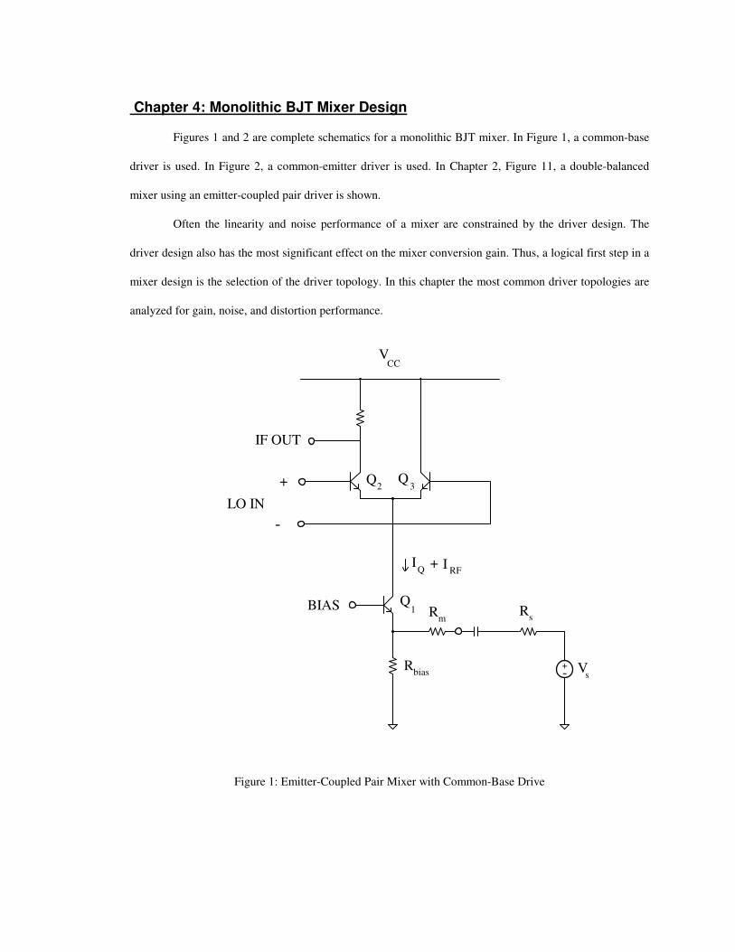
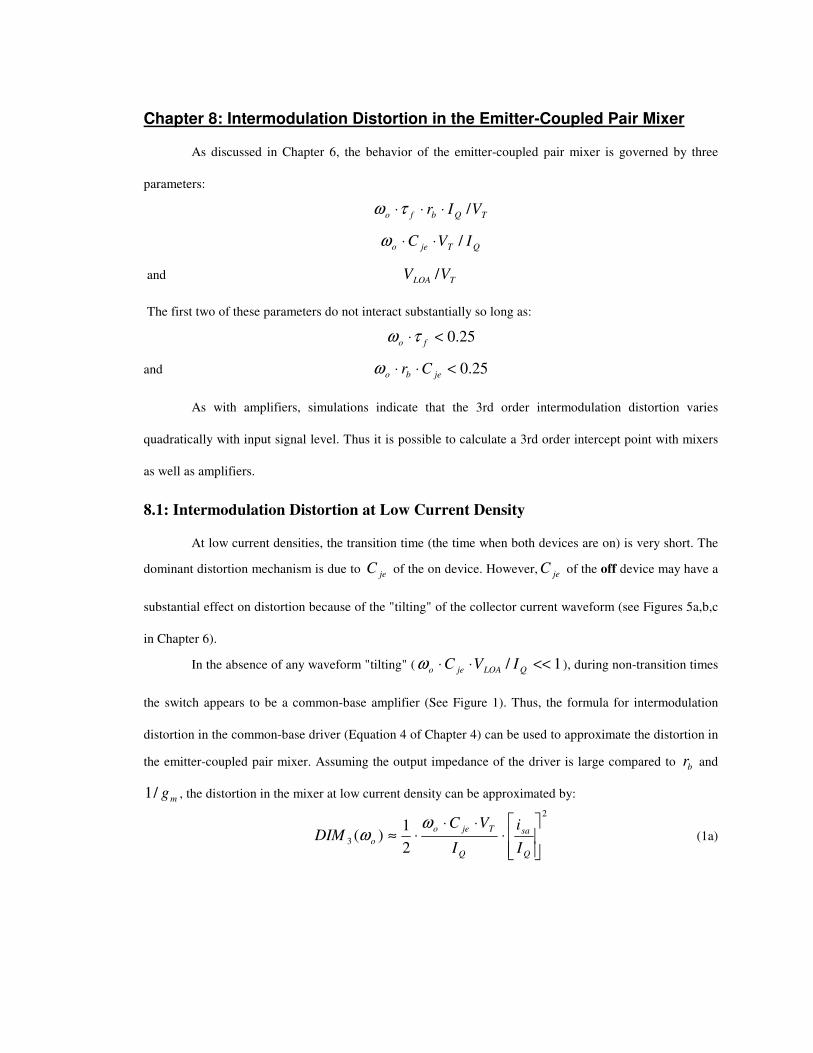
Chapter 4: Monolithic BJT Mixer Design
Figures 1 and 2 are complete schematics for a monolithic BJT mixer. In Figure 1, a common-base
driver is used. In Figure 2, a common-emitter driver is used. In Chapter 2, Figure 11, a double-balanced
mixer using an emitter-coupled pair driver is shown.
Often the linearity and noise performance of a mixer are constrained by the driver design. The
driver design also has the most significant effect on the mixer conversion gain. Thus, a logical first step in a
mixer design is the selection of the driver topology. In this chapter the most common driver topologies are
analyzed for gain, noise, and distortion performance.
LO IN
Q Q2 3+
-
+-
BIAS
Vs
Q1
IQ
+ IRF
Rm
Rbias
VCC
IF OUT
Rs
Figure 1: Emitter-Coupled Pair Mixer with Common-Base Drive
Page 35
LO IN
Q Q2 3+
-
VCC
IF OUT
+- Vs
50 ΩQ
1
VBE (ref)
Lb
Le
20 pF
1 KΩ
Figure 2: Emitter-Coupled Pair Mixer with Common-Emitter Drive
4.1: Common-Emitter Driver
Common-emitter drivers have the advantage of providing low noise and high gain. Also, at high
frequencies, the linearity performance of the common-emitter is quite good.
The linearity of the common-emitter driver is identical to the common-emitter amplifier analyzed
in Chapter 3.
The current gain of a common-emitter amplifier is given by:
fo
oi
sa
τβ
β
⋅⋅+=
1
Page 36
If the collector-base junction capacitance is neglected, then the input impedance is:
sC
sLLLrg
sLsrsZ ebTeb
m
ebin⋅
+⋅++⋅+≈
+⋅⋅+=
π
ωβ1
)(1
)()(
As in Chapter 3, an input match is obtained when the emitter inductance is:
tbse rRL τ⋅−= )(
and the total inductance is given by:
to
be LLτω ⋅
=+2
1
4.2: Common-Base Driver
Common-base drivers are advantageous when wideband operation is required. Common-base
stages provide a nearly constant input impedance and gain.
The input impedance of the common-base stage in Figure 1 is:
f
fb
mmin
s
srg
RsZτ
τ
⋅+
⋅⋅+
+=1
1
)( (1)
The current gain is given by:
f
is
aτ⋅+
=1
1 (2)
Note that if 1=⋅ bm rg , the input impedance is a constant resistance that is independent of frequency. For
smaller devices (which have a larger rb ) the input impedance will have an inductive component with
fbrL τ⋅= . Broadband impedance matching is achieved when smm RgR =+ /1 .
The distortion of the common-base amplifier is obtained by applying Equation 21 from Chapter 3
with bmsbe rRRZ ++= and mse RRZ += . Therefore:
2
121213 )2(2
1)(1)(
4
1),(
⋅⋅⋅⋅−⋅−⋅−⋅⋅⋅=
Q
co
I
ijjjjDIM ωκωωκωκωω (3)
πω
ωωκ
CjrRRV
IRR
rRRCjj
bms
T
Q
ms
bmsje
⋅⋅⋅+++⋅++
++⋅⋅⋅+≡⋅
)()(1
)(1)(
Page 37
If Tωω << and 1/)( >⋅+ TQms VIRR then 1)( <<⋅ωκ j and the distortion can be approximated
by:
[ ]
222
23 1/)(1
1
4
1)(
⋅
++⋅
⋅
⋅⋅+
⋅++⋅≈
Q
c
ms
b
Q
Tjeo
TQms
oI
i
RR
r
I
VC
VIRRDIM
ωω (4)
The first of the two terms in Equation 4 is due to the exponential relationship of voltage and current in the
bipolar device. The latter term represents a distortion mechanism which gives distortion that increases
linearly with frequency. At low frequencies the distortion in the common-base stage is quite low, as the
nonlinear transconductance tends to be canceled by the nonlinear input impedance. At high frequencies the
distortion rises, because the input impedance is linearized by jeC while the transconductance remains
nonlinear. The distortion is 3dB above its low frequency value when:
jebms CrRR ⋅++=
)(
1ω (5)
The distortion in the common-base is independent of ω∆ , the separation of the two input
frequencies.
Distortion in the common base rises monotonically with increasing frequency. At low frequencies
the distortion is quite superior to an undegenerated common-emitter configuration. However, distortion in
the common-emitter stage tends to decrease with frequency (see Chap. 3, Figure 4) while distortion in the
common-base increases.
It is interesting to observe the frequency at which the two configurations have equal distortion. For
this calculation, bond wires are neglected. Therefore:
be
T
eQ
beje
RCsV
RI
RCss
⋅⋅+⋅
+
⋅⋅+=
π
κ
1
1)(
κ is the parameter used in Chapter 3. For the common-base, ∞→beR (if the emitter is fed from an ideal
current source) and if Tωω << then:
Q
Tjecb
I
VCjj ⋅⋅⋅≈⋅ ωωκ )(
Page 38
and
Q
Tje
Q
ccb
I
VC
I
iIM
⋅⋅⋅
⋅≈−
ω2
34
1 (6)
For the common-emitter without degeneration:
)(1
)(1)(
bs
bsje
rRCs
rRCss
+⋅⋅+
+⋅⋅+=
π
κ
At high frequencies this can be approximated by:
π
κC
Cs
je≈)(
And using Equation 21 from Chapter 3:
22
38
1
⋅
⋅≈−
πC
C
I
iIM
je
Q
cce (7)
The two stages have equal distortion for:
π
ωωC
C je
T⋅
⋅=2
(8)
For typical low-noise designs jeCC ⋅≈ 2π and the distortions are equal for:
f
T
τ
ωω
⋅≈≈
8
1
4
That is, the distortion of the common-base and common-emitter are about equal at 25% of the
actual device's Tω or 12.5% of the typical device's peak Tω . For a modern silicon bipolar process with
pSf 11=τ , the distortions of the two stages are equal at 1.8GHz.
In common-emitter stages, the bond-wire inductance will reduce the distortion significantly below
that predicted by Equation 7 for frequencies near πCLL eb ⋅+ )(/1 . However, in common-base stages
the bond-wire inductance has little effect on the distortion. Therefore, bond-wires may allow the common-
emitter stage to exhibit lower distortion than the common base for an octave or two below the frequency
given by Equation 8.
It should also be noted that the distortion of the two stages was compared for constant output
current levels. Since a common-emitter stage has current gain, its input intercept will be substantially lower
than its output intercept. A common-base stage has unity current-gain, thus its input intercept (when
Page 39
expressed as a current) is identical to its output intercept. However, since the common-base has no current
gain, a high-gain preamp is necessary for adequate overall front-end gain. If a common-emitter driver is
used, a lower-gain preamp (or no preamp at all) is desirable in order to maintain an adequate third order
intercept point for the front-end.
The noise figure of a common-base driver is given by:
2
22
2
222
)(
1
1s
mbsbnmbs
m
cnmnbn
v
RrZij
RrZ
givv
F
++⋅+⋅
+++⋅++
+=ωβ
(9)
Equation 9 is almost identical to Equation 7a of Chapter 3. The reason for this is that the
equivalent input noise generators are identical for all three of the basic transistor configurations (common-
emitter, common-base, and common-collector).iv There is an additional term due to the noise of the emitter
series resistor used for matching. The equations in Chapter 3 hold for the common-base so long as br is
replaced by mb Rr + .
However, distortion and matching considerations are different for the common-base than for the
common-emitter. For low distortion in the common-base it is necessary that 1)( >>+⋅ msm RRg and
1/ <<⋅⋅ QTjeo IVCω . Matching requires that smm RgR =+ /1 . Together these conditions mandate
that sm RR ≈ , and jeC must be small. These requirements are in direct opposition to the requirements for
low noise.
A compromise must be made when choosing between a large device (which offers minimum
noise) and a minimum size device (which offers minimum distortion). A reasonable choice is a device size
that makes the two terms in Equation 4 approximately equal. That is:
so
jeR
C⋅⋅
≈ω2
1 (10)
For this value of jeC the distortion is approximately:
2
324
1)(
⋅
⋅⋅
⋅≈
Q
c
sQ
To
I
i
RI
VDIM ω (11)
Distortion is reduced by increasing the bias current.
Page 40
4.3: Design Example For Common Base Driver
Suppose that the minimum size transistor available in a given process has the following parameters:
400=br , fF33=jeC , ps12=fτ , 100=oβ .
The design frequency is GHzfo 1= . Applying Equation 10:
fF796≈jeC
The device area relative to a minimum size device is then:
24=A
0.1 1 10 100
2
3
4
5
6
7
I c
Noise Figure
(dB)
Figure 3: Noise Figure vs. Bias Current for a Common-base stage
The noise figure vs. bias current is plotted in Figure 3. Note that the noise figure, while still fairly
good, is not as low as the common-emitter stage discussed in Chapter 3. This is not surprising, since the
common-emitter stage was optimized for noise performance. The noise figure in the common-base increases
monotonically with increasing bias current.
Page 41
The third order intercept point vs. bias current is plotted in Figure 4. Note that the intercept point
increases rapidly for increasing bias current. Thus, there is a tradeoff between linearity, power, and noise.
The bias current should be chosen to be the minimum value that gives adequate linearity. The effect of the
driver's intercept point on the system depends on the preamp gain. As the preamp gain is increased, a higher
mixer bias current is required for an adequate system intercept point. Therefore, the preamp gain should not
be set too high. System gain and noise considerations generally set the minimum gain of the preamps.
Typically the preamp will have 15-20 dB of gain.
0.1 1 10 100
20
10
0
10
20
30
40
I c
Third Order
Intercept
(dBm)
Figure 4: Third Order Intercept vs. Bias Current for a Common-base stage
4.4: Emitter-Coupled Pair Driver
An emitter-coupled pair driver is shown in Figure 5. Emitter-coupled pairs are commonly used to
drive double-balanced mixers (such as the one shown in Chapter 2, Figure 11). Emitter-coupled pairs easily
convert unbalanced signals to balanced signals or vice-versa. Unfortunately, the emitter-coupled pair has a
Page 42
greater number of noise sources compared to a single ended amplifier; hence, it tends to have poorer noise
performance. To make matters worse, it is difficult to match the emitter-coupled pair's high input impedance
to a typical source impedance. It is common practice to use a shunt resistor at the input to obtain a match.
Unfortunately, such a "brute-force" approach further degrades noise performance.
Q1
IQ
Q 2Vrf
Re R
e
Rm
Figure 5: Emitter-Coupled Pair Driver
To quantify the effects of "brute-force" matching, suppose that the amplifier without the shunt
resistor has equivalent input voltage and current noise sources vn and in . Assuming that 0=sX , the
noise figure without matching resistor is:
2
2
1
s
snn
v
RivF
⋅++= (12)
Assuming that sm RR = , the noise figure with matching resistor is:
2
22
2
s
snn
v
RivF
⋅+⋅+= (13)
Where:
2121
21 enen
m
cncnbnbnn vv
g
iivvv ++
+++≈
Page 43
)(
11
ωβ ⋅+=
j
iii cnbnn
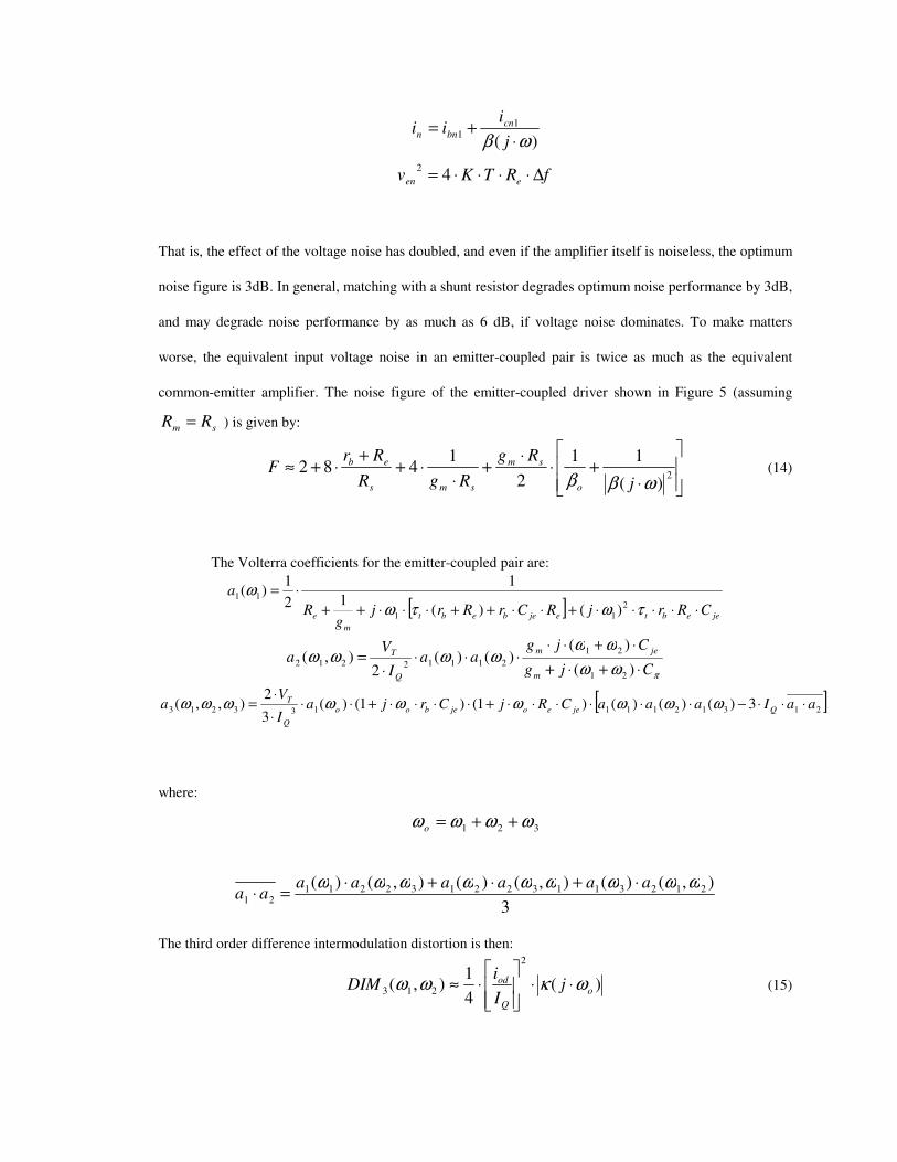
fRTKv een ∆⋅⋅⋅⋅= 42
That is, the effect of the voltage noise has doubled, and even if the amplifier itself is noiseless, the optimum
noise figure is 3dB. In general, matching with a shunt resistor degrades optimum noise performance by 3dB,
and may degrade noise performance by as much as 6 dB, if voltage noise dominates. To make matters
worse, the equivalent input voltage noise in an emitter-coupled pair is twice as much as the equivalent
common-emitter amplifier. The noise figure of the emitter-coupled driver shown in Figure 5 (assuming
sm RR = ) is given by:
⋅+⋅
⋅+
⋅⋅+
+⋅+≈
2)(
11
2
1482
ωββ j
Rg
RgR
RrF
o
sm
sms
eb (14)
The Volterra coefficients for the emitter-coupled pair are:
[ ]jeebtejebebt
m
e CRrjRCrRrjg
R
a
⋅⋅⋅⋅⋅+⋅⋅++⋅⋅⋅++
⋅=
τωτωω
2
11
11
)()(1
1
2
1)(
πωω
ωωωωωω
Cjg
Cjgaa
I
Va
m
jem
Q
T
⋅+⋅+
⋅+⋅⋅⋅⋅⋅
⋅=
)(
)()()(
2),(
21
21
21112212
[ ]21312111133213 3)()()()1()1()(3
2),,( aaIaaaCRjCrja
I
Va Qjeeojeboo
Q
T ⋅⋅⋅−⋅⋅⋅⋅⋅⋅+⋅⋅⋅⋅+⋅⋅⋅
⋅= ωωωωωωωωω
where:
321 ωωωω ++=o
3
),()(),()(),()( 21231132213221121
ωωωωωωωωω aaaaaaaa
⋅+⋅+⋅=⋅
The third order difference intermodulation distortion is then:
)(4
1),(
2
213 o
Q
od jI
iDIM ωκωω ⋅⋅
⋅≈ (15)
Page 44
[ ] jebejebemebem
jeejeb
CrCRsCrRgCRrsRg
sCRsCrs
⋅⋅⋅⋅+⋅⋅⋅+⋅+⋅+⋅+
⋅⋅+⋅⋅⋅+=
ππ
κ2)(1
)1()1()(
So long as eb Rr << and 1<<⋅⋅ jeeo CRω , the distortion in the emitter-coupled pair is approximately
independent of the device size chosen.
4.5: Design Example For Emitter-Coupled Pair Driver
Consider an emitter-coupled pair driver that uses the same process as the common-base example.
In Figure 6 the distortion is plotted vs. device area for four different values of eR . The total bias current is
6.3mA. Since eR represents local feedback, its effect on distortion is a function of the loop gain. For this
feedback configuration, the loop gain is given by:
em RgT ⋅=
Notice that for device sizes between 10x and 100x, the distortion is relatively independent of area.
There appear to be two ways to achieve low distortion: use a small device, or use substantial
degeneration. While both approaches degrade noise performance, the latter appears to be a more viable
solution.
Page 45
1 10 100 1000
40
35
30
25
20
15
10
5
0
Area
T=0
T=1
T=3
T=10
IM3
(dB)
Figure 6: Distortion Vs. Device Area for an Emitter-Coupled Pair
To clarify this point, the noise figure is plotted against area in Figure 7. For small areas the noise
figure is very poor. This is a result of the voltage noise multiplication of the matching resistor and the
inherently higher voltage noise of the emitter-coupled pair. The optimum device area is around 150-200x,
and is approximately independent of T. The optimum noise figure is between 5-10 dB depending on the
amount of degeneration. A degeneration factor near 3 seems to be a good compromise, since a larger value
of degeneration does not improve the distortion much, but increases the noise figure substantially.
It is interesting to compare the performance of the emitter-coupled pair stage and the common-base
stage. Assuming equal total current of 6.3mA, the common-base stage has a noise figure of 4.5dB (see
Figure 3) and the distortion is down 40dB for 100% modulation (see Figure 4). Using an emitter-coupled
pair of area 100x (relative to the minimum size device) and degeneration factor 3, the noise figure is about
7.0dB (Figure 7), and the distortion is down only 24dB (Figure 6). Thus the dynamic range of the emitter-
coupled pair is 10.5dB less than the common-base.
Page 46
Clearly the emitter-coupled pair provides inferior performance to both the common-base and
common-emitter amplifiers. The noise performance is the worst of the three stages. The linearity at best
equals the common-base (when heavy degeneration is used). When the degeneration is reduced because of
noise considerations, the linearity is much worse than the common-base. Nonetheless, the emitter-coupled
pair is widely used for double-balanced mixers since it makes use of external BALUNS unnecessary.
1 10 100 10000
5
10
15
20
1
T=0
T=1
T=3
T=10
Noise
Figure
(dB)
Area
Figure 7: Noise Figure vs. Device Area for an Emitter-Coupled Pair ( 6.3mA=QI )
Page 47
Chapter 5: Noise Analysis of Nonlinear Circuits:
Active mixers are widely used for down conversion in UHF and microwave receivers. In contrast
to passive mixers, active mixers provide gain as well as frequency conversion. A mixer is shown
schematically in Figure 1. The mixer has an RF (radio-frequency) and LO (local-oscillator) input ports and
an IF (intermediate frequency) output port. Ideally the mixer should produce only a scaled version of the
product of the two input signals. However, real mixers add spurious signals and random noise to the desired
output signal.
Local Oscillator Input
RF Input IF Ouput
Mixer
Figure 1: Basic Mixer Structure
It is desirable to be able to predict the noise performance of a given mixer design. Amplifier noise
analysis techniques do not apply to mixers, because the presence of a large LO signal causes substantial
change in the active devices' operating points over a period. Techniques that have been previously presented
have the disadvantage that they are non-systematic, and numerically ill-conditioned.v,vi
Additionally, these
methods fail for shot noise in the absence of a high-Q tuned circuit.
In this chapter a method is presented that is numerically efficient and well conditioned, systematic,
and accurate. A significant advantage of this technique is that one simulation yields information on the
mixer performance for all RF and IF input frequencies. Previously presented analysis techniques required a
separate simulation for each RF input and IF output frequency of interest.vii
Page 48
5.1: State Equations for Mixers:
It is a basic result of circuit theory that any circuit made up of elements that are either current
controlled or voltage controlled can be described by a system of state equations of the form:viii
( )VIFdt
Id vvrr
,= (1a)
)(ICSout
r= (1b)
Ir
is the vector of state variables, Vr
is the vector of signal voltages applied to the circuit, and outS is the
output signal. State variables are made up of capacitor voltages (or charge) and inductor currents (or flux).
In bipolar transistors, the state variable corresponding to the voltage across πC may be replaced by the
collector current through the algebraic transformation:
)1( −⋅= TV
V
sc eII
π
An alternative formulation known as modified nodal analysis uses node voltages and inductor
currents. Then Ir
is the vector of node voltages and inductor currents. The relationship between modified
nodal analysis equations (MNA) and state variable equations is quite simple. Modified nodal analysis
produces one redundant equation for each node that has no capacitive element attached to it. Despite the
large matrix structure created, MNA is currently implemented in many CAD packages (e.g., SPICE) and
such a formulation is desirable for integration into the computer code of such packages.
All mixers operate by use of a large LO signal that modulates the operating point of the active
devices (or diodes for passive mixers) in the mixer. In the absence of RF overload, the LO is the only large
signal applied to the mixer. Noise sources in the mixer can be thought of as small signals applied to an
otherwise noiseless mixer circuit. Because of the large LO signal, linear noise analysis of mixers based on a
fixed operating point is not possible. Analysis of mixers using available non-linear techniques is
numerically ill-conditioned, since a small numerical error relative to the LO amplitude may be quite large
Page 49
relative to other signals in the circuit. Hence, it is desirable to obtain a method that works independently on
the large and small signals. Such a method is now presented.
Assuming a large LO signal and a small RF signal, the state equation for mixers can be written:
[ ])(),(),()(
tvtVtIFdt
tIdrfLO
vrr
= (2a)
[ ])()( tICtSout
r= (2b)
Normally, the state of the mixer is determined primarily by the LO, with the RF signal causing only
a small perturbation. Suppose )(tIQ
r is the state vector in the absence of an RF signal (henceforth referred
to as the quiescent state vector). That is, rI tQ ( ) is the solution to:
[ ]0),(),()(
tVtIFdt
tIdLOQ
Qvr
r
= (3)
Then the state vector with the RF signal included is:
)()()( titItI Q
rrr+=
where: [ ] [ ]0),(),()(),(),()(dt
(t)idtVtIFtvtVtitIF LOQrfLOQ
rrrvrr
−+=
Using a first order Taylor Expansion of F about the quiescent state gives:
)()()()(dt
(t)idtvthtit rfo ⋅+=
rro
r
G (4a)
where
)(tQj
i
jidI
dFG =,
)(
)(
tQrf
odv
Fdth
rr
=
Page 50
The notation )(tQ is used to mean that the derivative is evaluated at the quiescent state.
A similar analysis starting with Equation 2b gives the small-signal output as:
)()()( titctsout
ro
r= (4b)
where
)(
)(tQId
dCtc v
r=
and " o " indicates matrix multiplication.
Second order Taylor expansion terms are generally negligible if the RF signal voltage (or noise
voltages) is sufficiently small that nonlinearities of the circuit are not significantly excited. Because the RF
signal voltages and internal noise voltages in the mixer are small, superposition applies, and each one can
be analyzed separately.
Equations 4a&b are linear time-varying equations. The coefficients vary with time in a manner
determined by the applied LO signal and the circuit configuration. If the LO signal is periodic (as is usually
the case), the coefficients in Equations 4a&b become periodic and the system of equations is a linear
periodically time-varying system or LPTV. As presented in this chapter, Equations 4a&b are derived from
differentiation of the state equations of the system. However, these equations may be obtained directly from
the circuit by replacing each element of the nonlinear circuit by its linear time-varying equivalent circuit.
Thus, the mixer circuit equations are solved in two steps:
Step 1: Solve the large-signal system of equations in Equation 3. The RF and noise sources are turned off
(only the LO source is left on), and all of the state variables are solved as a function of time for one LO
period.
Page 51
Local Oscillator Input
RF Input
IF Ouput
Mixer
Step 1
Figure 2: First step in mixer performance calculation
Step 2: Solve the small signal time-varying circuit equations (given by Equation 4, or from a linearized
circuit model) for the RF signal and each noise source. Because of the linearity of Equation 4, superposition
applies to each small-signal source.
The solution of step 1 is quite straight-forward. Many standard CAD packages can be used to
obtain the steady state response to the LO input. The solution of step 2 is currently not implemented in any
commercial CAD package. In the remainder of this chapter, two related techniques will be demonstrated for
solving LPTV systems for both deterministic and stochastic input signals. The first technique is more
efficient and well conditioned, while the latter is easily implemented using available CAD packages.
5.2: Equations for Linear-time Varying Systems:
For an LTV system the input-output relation is given byix
:
duuxuthty ∫∞
∞−
⋅= )(),()( (5)
The input-output relation of Equation 5 is similar to the standard convolution used in a linear time-
invariant system. However, the value of the impulse response is a function of both the launch time of the
Page 52
impulse, u, and the observation time, t. In a time-invariant system, the impulse response is only a function
of the difference between the observation time and the launch time.
)(),( uthuth lti −=
Under the above condition, Equation 5 reduces to the familiar convolution integral.
In an LTV system the impulse response may look quite different for different launch
times. For mixers with periodic LO excitation, the impulse response is periodic in launch time, and thus can
be seen as a function of the launch phase (the phase of the LO at launch time). In the frequency domain the
relationship between the output and input spectrum is given by:
rfrfrfifif dXHY ωωωωω ∫∞
∞−
⋅= )(),()( (6)
X and Y are the Fourier Transforms of input and output signals, and H is given by:
dtedueuthHtjuj
rfififrf ⋅⋅−
∞
∞−
∞
∞−
⋅⋅⋅
⋅
⋅= ∫ ∫
ωω
πωω ),(
2
1),(
A derivation of Equation 6 is given in Appendix A.
From Equation 6 it is seen that for a general linear time-varying system, a single input frequency
produces a continuous spectrum of output frequencies, not just a single output frequency as in the case of an
LTI system.
For periodic LO excitations of frequency o , the frequency domain equations, which are derived in
Appendix B, become:
∑∞
−∞=
⋅+⋅=n
oififnif nXHY )()()( ωωωω (7)
where
dvedueuvgT
Hvjunj
T
ifnifo
⋅⋅−∞
∞−
⋅⋅⋅
∫ ∫
⋅=
ωωω0
),(1
)( (8)
Page 53
),(),( uuvhuvg +=
In an LPTV system a given input frequency produces a discrete set of output frequencies,
separated in magnitude by oω . The output spectrum is a linear superposition of shifted and filtered
versions of the input spectrum. For each shift the frequency response of the system is given by )(ωnH ,
where n is the number of LO frequencies that the input spectrum is shifted.
Another point of view is that multiple input frequencies given by:
iforf n ωωω ±⋅= (9)
are all down-converted to the IF output frequency through modulation against the n'th LO harmonic. This
relationship is especially important in mixer noise analysis, since noise at a number of different input
frequencies may contribute output noise at the intermediate frequency. Frequencies of particular interest
are: ifrf ωω = and iforf ωωω ±= corresponding to n=0 and n=1. The latter two frequencies are the
input-signal frequency and the image frequency. The existence of the image frequency is problematic in low
noise mixer design since the noise from that frequency contributes to the output. Often the noise at the
image frequency contributes equally to the noise at the RF signal frequency, degrading the noise figure by 3
dB. Input noise at the intermediate frequency can be a significant problem in unbalanced mixers; however,
in balanced mixers the noise from the intermediate frequency is ideally canceled at the output.
For stationary noise the input-output relation is:
∑∞
−∞=
⋅+=n
oifxifnify nSHS )()()(2
ωωωω (10)
Sx is the input spectral density and Sy is the output spectral density.
If the input noise is white (constant spectral density), and if the output frequency is much lower than
any time constants in the system, then the output spectral density can be approximated by:
Page 54
duedvuvgT
SHSSunj
T
xo
n
nxoyoo ⋅⋅⋅
∞
∞−
∞
−∞=∫ ∫∑
⋅⋅=⋅≈ ω
0
2),(
1)0(
This approximation is often useful for downconversion mixers.
The impulse response function, ),( uth , together with Equations 7 and 8, are sufficient to describe
the small signal input-output behavior of the mixer for all possible excitations.
Since the impulse response of a mixer depends on the location of the input excitation, a separate
calculation for each noise source is necessary. Often a number of noise sources can be lumped into a single
source, thus reducing the number of impulse responses that must be calculated. Circuit symmetry can also
be exploited to further reduce required calculation.
5.3: Obtaining the Impulse response of an LTV system
A theoretical approach that uses state equations to obtain the impulse response is presented in this
section. This method, while efficient and theoretically sound, is currently not implemented in any
commercially available CAD package.
Referring to Equation 4a&b, the value of the small-signal state vector and impulse response at
observation times just after the launch time can be shown to be:
)(),( thuui o
rr=+
(11a)
)()(),( uhucuuh o
ro
r=+
(11b)
The second argument of the function ri corresponds to the launch time. For observation times t > u, the
differential equation is:
),()(dt
u)(t,idutit
ro
r
G= (11c)
The impulse response is obtained from the linearized relation:
),()(),( utitcuthr
or
= (11d)
Page 55
Equation 11a-d constitute a homogenous initial value problem. These equations can be solved by
standard numerical ODE methods such as the trapezoidal method. The values of )(tcr
, )(tG , and )(tho
r
are periodic, and depend on the large-signal ODE solution of Equation 3. The values of these functions are
calculated over an LO period and then stored.
5.4: Fourier Transform Analysis
Once the impulse response is calculated for launch times that span the range of all LO phases, the
response must be processed by a two-dimensional fast-Fourier transform to obtain the system function as
given in Equation 8.
Ideally, the impulse response would be calculated for all launch times in [0,T] and for all
observation times. For causal systems it is not necessary to consider observation time prior to the launch
time. Since it is not possible to express a closed form solution of the impulse response for even simple
mixer circuits, the impulse response values are calculated at finite intervals in both observation time and
launch time. This discretization introduces aliasing errors. Further, it is necessary to assume that at
observation time t=M+u, for some M, the impulse response decays to a negligible value. For accurate
results M must be chosen to be much larger than the largest time constant in the circuit (under worst case
conditions). If the interval between successive observation time points is chosen to be dV, and the interval
between successive launch times is dU, then the total number of points required to describe the impulse
response is:
dVdU
TMN LO
⋅
⋅=
Clearly for a fixed value of N, there is a tradeoff between the conflicting requirements of large M,
and small dU and dV. Choosing an M that is too small will cause "blurring" in the frequency domain due to
convolution with a sinc function. The value of dV should be chosen to be much smaller then the inverse of
the IF bandwidth, and dU should be chosen to be much smaller than the inverse of the RF bandwidth.
Page 56
Choosing dU or dV too large will cause aliasing. It is best to choose M, dU, and dV to balance out the three
errors, so that no single one dominates.
Often only low output frequencies are of interest. In such a case a low pass filter is placed at the
output, and the sampling interval in the observation time, dV, may be made substantially larger. For
simulation purposes high-Q IF filters should be avoided, since they cause the impulse response to ring, and
thus require a very large value of M (much larger than the inverse of the IF bandwidth). A three-pole low-
pass IF filter at three times the LO frequency yields a good tradeoff between accuracy and simulation time.
M is usually chosen to be an LO period, and dV is chosen to be 1/32 of an LO period. The three-pole filter
reduces spectral components sufficiently to prevent aliasing. Figure 3 illustrates the relationship between
the grid chosen in the time domain and a corresponding grid obtained in the frequency domain after a two-
dimensional FFT is performed.
Time Domain
dV
0 M
V
U
dU
0
T
Observation Time
LaunchTime
Frequency Domain
1/M2*dV
n
-P/2+1
P/2
Output Frequency
LO Harmonics
if
0
0
1____2*dV
-1____
Figure 3: Grids in Time and Frequency Domain
The two dimensional FFT is obtained by calculating an FFT of the rows of h(t,u) and then an FFT
of its columns. Care must be taken to observe the exponential signs and scaling factor for each direction of
Page 57
the FFTs. The calculation complexity can be shown to be on the order of )log(NN ⋅ . Usually the time
required for the FFT is small compared with the time required to obtain the impulse response.
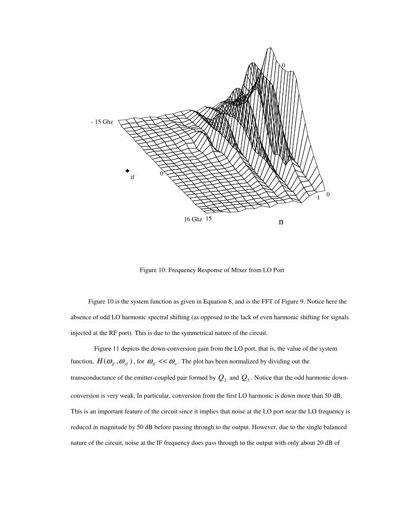
The result of the FFT is a two-dimensional grid in the frequency domain. The axes are if and n,
where n is the number of LO frequencies by which the input spectrum has been shifted (see Equation 7).
The output frequency is discretized with spacing of 1/M, and spans the range from )2/(1 dV⋅− to
)2/(1 dV⋅ . The value of n spans -P/2+1 to P/2, where dUTP /= . The output spectral density is then
obtained through a weighted sum of the columns:
∑+−=
⋅+=2/
12/
2
)()()(P
Pn
oifxifnify nSHS ωωωω (12)
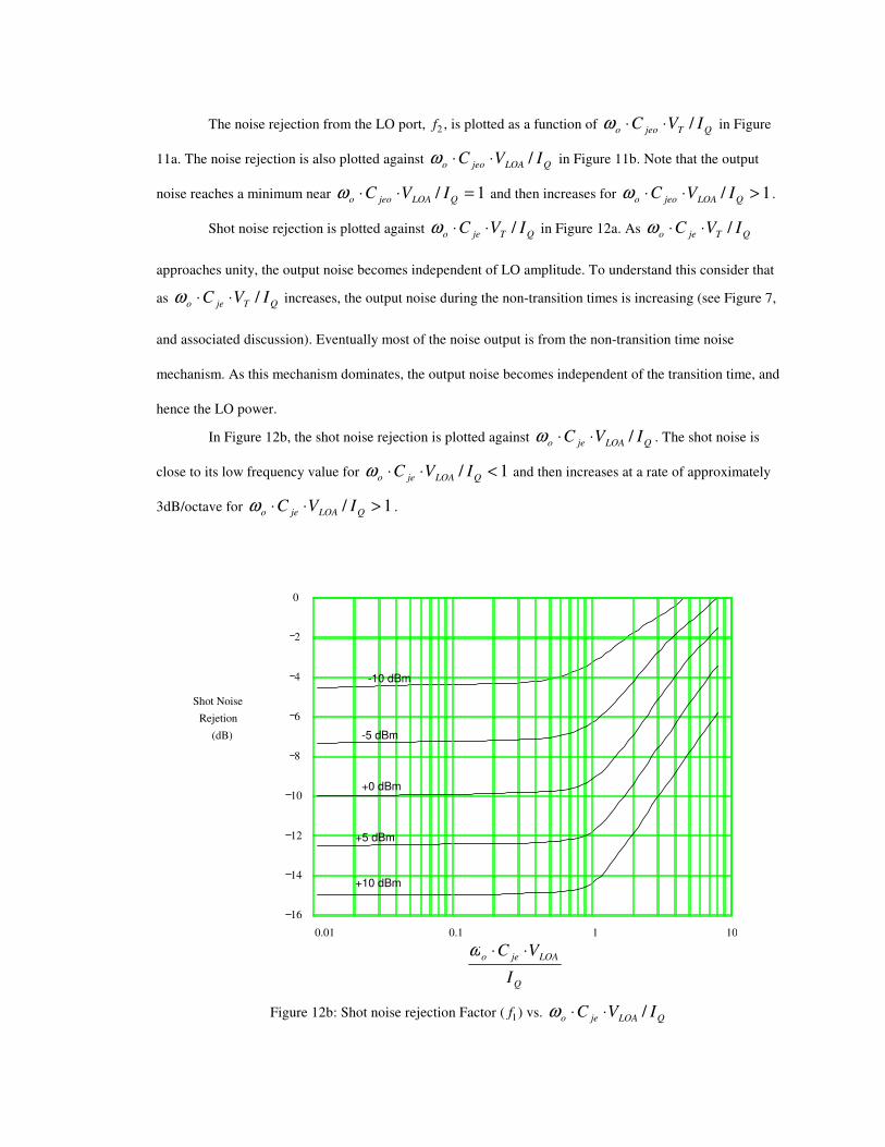
5.5: Summary of Steps Required to Calculate Output Noise in a Mixer
Step 1: Solve the large-signal deterministic problem:
[ ]0),(),()(
tVtIFdt
tIdLOQ
Qvr
r
=
Step 2: Solve the homogenous time-varying initial value problem for TdUdUu ,...,2,,0 ⋅= , and
MudVudVuut +⋅++= ,...,2,,
),()(dt
u)(t,idutit
ro
r
G= with )()( uhui o
rr=
then:
),()(),( utitcuthr
or
=
Step 3: Do a two-dimensional FFT on the impulse response:
Page 58
dudveeuvgT
H
Tvjunj
M
ifn
ifo∫ ∫⋅⋅−⋅⋅⋅⋅=
0 0
),(1
)(ωωω
),(),( uuvhuvg +=
Step 4: Evaluate the output noise spectrum:
∑+−=
⋅+=2/
12/
2
)()()(P
Pn
oifxifnify nSHS ωωωω
dUTP /=
5.6: Conversion Gain and Input Referred Noise Spectral Density
The conversion gain and noise figure are also available. Recall:
∑∞
−∞=
⋅+⋅=n
oififnif nXHY )()()( ωωωω (7)
Therefore for first harmonic down conversion (or up conversion) the gain is simply:
)()(
)(1 if
rf
if
ic HX
Ya ω
ω
ω±== (13)
The +/- is chosen depending on the relative relationship of the RF and LO frequency. If the RF frequency is
above the LO frequency than +1 is used, whereas if the RF frequency is below the LO frequency than 1−
is used. For low IF frequencies, there is negligible difference between the 1H and 1−H .
The input referred noise is then:
( )2
1 )(
)(
if
ifx
ifeq
H
SS
ω
ωω
±
= (14)
Page 59
5.7: Simplified Low Frequency Theory
First consider the case where the intermediate-frequency is sufficiently low so that 1max <<⋅τω if .
Where maxτ is the longest time constant in the circuit. In this case, Equation 8 simplifies to:
duedvuvhT
HHunj
T
nifno ⋅⋅⋅
∞
∫ ∫ ⋅
⋅=≈ ωω
0 0
),(1
)0()(
The conversion gain is:
duedvuvhT
Huj
T
ifo ⋅⋅
∞
∫ ∫ ⋅
⋅≈ ωω
0 0
1 ),(1
)(
If the noise source is white, with spectral density Sxo , then Parseval's theorem can be used to express the
output spectral density as:
dudvuvhT
SS
T
xoyo ∫ ∫
⋅=
∞
0
2
0
),(
In the case where 1max <<⋅τωo , further simplifications are possible. Because the LO period is
much longer than the impulse settling time, the input-output relation can be approximated by:
)()()( uxuhuy ⋅= (15)
The distinction between launch time and observation time is no longer necessary, as the only time
when anything is observed is the launch time. This is a valid approximation when the impulse response
duration is much less than the time it takes for the mixer circuit to significantly change its state. In other
words, for this approximation to be valid, none of the large-signal state variables may change significantly
over the decay time of the impulse response. The impulse response, )(uh , may be thought of as the gain
from the RF port (or point of the noise source) to the IF output port. The gain is a function of the LO phase.
In the frequency domain the input-output relationship and the output noise spectral density are:
∑∞
−∞=
⋅+⋅=n
oifnif nXHY )()( ωωω (16)
∑∞
−∞=
⋅+⋅=n
oifxnify nSHS )()(2
ωωω (17)
where,
Page 60
dtethT
Htnj
T
no ⋅⋅⋅
∫⋅= ω
0
)(1
(18)
If the input noise spectrum is white then the output noise spectrum is white, and its density is given by:
dtthT
SS
T
xoyo ∫⋅⋅=0
2 )(1
The Hn 's are the Fourier coefficients of the gain vs. time and are independent of the IF frequency.
The gain vs. time is obtainable using small-signal analysis. The operating point at each launch time is held
fixed. In the absence of charge storage elements, the analysis is drastically simplified. However, it is still
necessary to solve a large-signal problem. Strictly speaking, this method is accurate only when the LO and
output periods are much longer than the longest time constant in the circuit. However, the qualitative
characteristics of a mixer at high frequencies often resemble those at low frequencies. Therefore, much
information can be obtained by a simple low frequency analysis.
5.8: Results
Currently, no CAD package is available to implement steps 2-4 of the above method, although a
modification in SPICE that currently works for the most rudimentary transistor models has demonstrated the
feasibility of a full implementation. In the interim, a technique that uses the standard SPICE to produce
results is used. This technique is presented below.
A single long transient run is performed. The LO signal is applied as well as a periodic pulse signal
at either the RF port or at a location where significant noise sources exist. The period of the pulse is slightly
longer than an LO period, so that the LO phase changes by dU for each launch:
dUTT LOpulse +=
The simulation is run for a total of P pulse periods:
LOLOpulsesimulation TPdUPTPTPt ⋅+=⋅+⋅=⋅= )1(
Page 61
P is chosen to be sufficiently large so as to avoid aliasing problems, as discussed in the section on
Fourier transform analysis. Typically a value in the range of 64 to 256 is adequate. Before the pulse
launching begins, several LO cycles must be passed through in order to let the mixer settle into steady state.
It is assumed that the impulse response of the circuit settles to a negligible value within a single pulse
period. If this is not the case, a longer pulse period must be chosen, with a corresponding increase in
simulation time. The response of each simulation period corresponds (approximately) to the impulse
response of the mixer at evenly stepped LO phases.
I n order to minimize the number of data points in the observation time, a three-pole maximally flat
IF filter at three times the LO frequency is used. With this filter it is necessary to sample 32 data points per
pulse period for 0.1% accuracy. Additionally, the impulse response of this filter settles to within 0.1% of the
impulse height within an LO period, indicating suitability for the above technique. The response roll-off
caused by this filter is easily corrected for, and the only limitation of this filtering technique is that data is
not available for output frequencies above 16 times the LO frequency. However, one is usually only
interested in output frequencies either much lower than the LO frequency (for down conversion) or near the
LO frequency (for up conversion). In either of these two cases of interest, the IF filter adds no appreciable
error. For simulations, high-Q IF filters should be avoided, since they give long transient tails that consume
large amounts of simulation time.
For verification purposes an emitter-coupled mixer with common-base drive, shown in Figure 4,
was designed and fabricated. Transistor 1Q is chosen to be large in order to minimize its noise
contribution. The common base configuration was chosen for the input stage because of its superior
linearity. Transistors 2Q and 3Q were made somewhat smaller than 1Q in order to minimize distortion.x
The mixer was designed to operate at an RF frequency of 1GHz, although it will function for RF
frequencies up to 5 GHz. In this circuit configuration, most of the noise is contributed from the non-linear
portion of the circuit.
Page 62
+-
BIAS
LO IN
Vin
50 30
400
500
VCC
IF OUT
BIAS
50
3 mA
Q Q
Q1
2 3
Figure 4 : Schematic of Single-Balanced Mixer Configuration
The approach taken for analyzing the circuit in Figure 4 is to lump all noise sources that inject noise
at the emitter of 2Q and 3Q into a single equivalent current noise source. This noise includes all of the
noise from transistor 1Q and associated biasing, as well as the noise from the source. Noise sources that are
incident at the base of 2Q are lumped into a single noise source, and likewise for noise sources at the base
of 3Q . The noise sources include the Ω50 matching resistor and the noise from the base resistance of 2Q
and 3Q . A bandpass filter is used between the LO and the input port, so it does not contribute significantly
to the output noise. Calculation of these noise sources follows the standard linear methods as implemented
in SPICE. Care must be taken to consider the actual impedances presented looking out from the LO and RF
ports. In addition to the above three noise sources, the shot noise of 2Q and 3Q must be considered
separately. Because of the low operating currents and LO source impedance, the base shot noise of
Page 63
transistors 2Q and 3Q contributes negligibly. The collector shot noise of transistors 2Q and 3Q are
analyzed separately. In simulations of shot noise, the initial impulse is scaled by the value of the
instantaneous bias current through the device.
100 uV
5 ns
0 uV
13.2 nstime
Vout
Figure 5: Impulse Response of Single-Balanced Mixer for the RF port (8 of 64 launch phases)
In Figure 5 the impulse response of the mixer to impulses injected at the RF port is depicted for the
first 8 of 64 LO phases. The shape of the impulse response is essentially that of the IF filter which is a three-
pole maximally flat design. The LO frequency is 1 GHz. Figure 6 depicts the impulse response for all
launch phases in a three-dimensional plot. Note that a null exists for a large portion of launch phases. This
corresponds to the time when transistor 2Q is off.
Page 64
Observation Time
Launch
Phase
0ns1ns
Figure 6: Two Dimensional Impulse Response of a Mixer from RF Port
Figure 7 is the two-dimensional FFT of the impulse response shown in Figure 6. The effect of the
three pole low-pass IF filter has been compensated for, so that the intrinsic performance of the mixer at very
high IF frequencies may be observed. Recall that the axes are IF output frequency and n, the number of LO
harmonics that the input spectrum is shifted by. The plot depicts only positive values of n since it can be
easily shown from Equation 8 that the system function has symmetry about the origin. While values of n
from 0 to 31 are available, only those from 0 to 15 are plotted, since down conversion from harmonics
higher than the 15th is negligible. This suggests that aliasing is not a problem with the chosen point spacing.
Note spectral shift by an even number of harmonics of the LO is very weak. This is not surprising since the
symmetrical nature of this circuit tends to cancel out even LO harmonics.
Page 65
0
16 Ghz
-15 Ghz
if
0
15
n
1
Figure 7: Frequency Response of Mixer from RF Port
Figure 8 contains a cross section of Figure 7, with the IF frequency restricted to be much less than
1 GHz. This is of interest for down-conversion. This particular plot then is of the down-conversion gain vs.
input frequency (since for low IF frequencies the input frequency and spectral shift are nearly equal). Again
notice the small value of the down-conversion from even harmonics. The value of the down-conversion gain
for n=1 corresponds to the signal current conversion gain of the mixer (in this case -10 dB).
Page 66
0 2 4 6 8 10 12 14 16
70
60
50
40
30
20
10
n
dB
Figure 8: Down Conversion Gain Vs. LO Harmonic from RF Port
I t is clear from Figure 8 that this mixer is not balanced, since it passes signals at the IF frequency to
the output. The IF bandwidth of this circuit (in the absence of an IF filter) is close to the fT of the device
(10 GHz) for direct pass through. The IF bandwidth is reduced for larger values of n (the spectral shift).
Because of the generally wide IF bandwidth, one can conclude that the noise and signal behavior of this
mixer are essentially equivalent for down-conversion from 1 GHz and up-conversion to 1 GHz. However,
significant IF bandwidth limitations can occur due to parasitics at the collector of 2Q , making conversion
design somewhat more difficult.
Page 67
Observation Time
0ns1ns
Launch
Phase
Figure 9: Impulse Response of Mixer from LO Port
Besides noise coming into the RF port, there are noise sources incident at the LO port (such as
base-ohmic resistance noise of 2Q and 3Q ). The response to an impulse launched at the LO port is
depicted in Figure 9. As with the impulse response from the RF port, the basic shape of the impulse
response is due to the three-pole IF filter. Note that the impulse response has large peaks for launch phases
near 0 and 180 degrees. These correspond to launch times where both transistors 2Q and 3Q are active.
Page 68
16 Ghz
- 15 Ghz
if
n
0
15
1
0
0
Figure 10: Frequency Response of Mixer from LO Port
Figure 10 is the system function as given in Equation 8, and is the FFT of Figure 9. Notice here the
absence of odd LO harmonic spectral shifting (as opposed to the lack of even harmonic shifting for signals
injected at the RF port). This is due to the symmetrical nature of the circuit.
Figure 11 depicts the down-conversion gain from the LO port, that is, the value of the system
function, ),( rfifH ωω , for oif ωω << . The plot has been normalized by dividing out the
transconductance of the emitter-coupled pair formed by 2Q and 3Q . Notice that the odd harmonic down-
conversion is very weak. In particular, conversion from the first LO harmonic is down more than 50 dB.
This is an important feature of the circuit since it implies that noise at the LO port near the LO frequency is
reduced in magnitude by 50 dB before passing through to the output. However, due to the single balanced
nature of the circuit, noise at the IF frequency does pass through to the output with only about 20 dB of
Page 69
attenuation. Note that the gain of the emitter-coupled pair must be added to these attenuation factors to get
the actual input-output gain.
0 2 4 6 8 10 12 14
-70
-60
-50
-40
-30
-20
n
dB
Figure 11: Down Conversion Gain Vs. LO Harmonic from LO port
Page 70
6
8
10
12
14
16
18
20
22
24
-10 -8 -6 -4 -2 0 2 4
Theory
Measured
Noise Figue (dB)
LO Power (dBm)
6
Figure 12: Predicted and Measured Noise Figure vs. LO Power for Mixer
An additional simulation was run for shot noise sources. Special care must be taken with shot noise
as is discussed in the next section. Detailed results of shot noise simulations are not presented here.
Figure 12 depicts the predicted and measured noise figure vs. LO power and the two curves are in
good agreement.
5.9: Non-Stationary Noise:
Because of the time-varying nature of mixers, the statistics of the output noise are not constant, but
vary periodically. Such noise is not strictly stationary, but is cyclo-stationary.xi
Additionally, shot noise,
which is modulated by the collector current, is also non-stationary. This lack of stationarity may cause
problems in the analysis of mixer noise, since cyclo-stationary noise spectra at frequencies separated by the
LO frequency and its harmonics are correlated. Therefore, simple superposition of noise power from
different frequencies (as assumed in Equation 10) does not give a correct answer. Fortunately, there are two
ways to avoid this problem.
Page 71
First, there is a theorem that is easily proven. Cyclo-stationary noise that is passed through a filter
with bandwidth less than the frequency of the noise statistics becomes stationary. Usually the output noise is
passed through an IF filter with bandwidth much narrower than the LO frequency, and hence the output
noise is stationary. This is true for both up and down conversion.
Second, cyclo-stationary noise sources such as shot noise may be seen as modulated stationary
noise sources. The modulation must then be considered to be part of the mixer system that acts on this
noise, and thus must be included as a factor in the impulse response. The impulse response to the
hypothetical stationary noise source is given by:
Q
C
I
uIuthutg
)(),(),( ⋅=
Where )(uIC is the large signal collector current of the transistor being considered, and QI is the average
collector current over time. The input spectral density of the hypothetical stationary noise source is given
by:
QIqS ⋅⋅= 2)(ω
Page 72
5.10: Conclusion
A new technique for predicting noise performance in active mixers has been presented. A single
simulation gives information not only on the mixer's noise performance over a wide range of output
frequencies but also on the up and down conversion gain. The theory for a numerically efficient and well-
conditioned technique was shown. A technique that uses available CAD tools was also presented, and the
results of that technique are shown to be accurate for the mixer circuit configuration tested.
Appendix 5A: Derivation of Frequency Domain input/output Relation
Start with the time-domain input output relation:
∫∞
∞−
⋅= duuxuthty )(),()( (A1)
and the Fourier Transform relations:
∫∞
∞−
⋅⋅⋅⋅
≡ s
uj
S deXux S ωωπ
ω)(
2
1)( (A2)
∫∞
∞−
⋅⋅−≡ dtetxX
tj
ififω
ω )()( (A3)
Substituting Equation A1 into Equation A3 yields:
( ) dteduuxuthYtj
ifif ⋅⋅−
∞
∞−
∞
∞−
∫ ∫
⋅=
ωω )(),( (A4)
Then using Equation A2 gives:
ss
tjuj
if ddtduXeeuthY ifs ωωπ
ωωω
)(),(2
1)(
⋅⋅−∞
∞−
∞
∞−
∞
∞−
⋅⋅
∫ ∫ ∫⋅=
Page 73
Let:
dtdueeuthHtjuj
sififs
⋅⋅−∞
∞−
∞
∞−
⋅⋅
∫ ∫⋅≡ωω
πωω ),(
2
1),( (A5)
then it follows that:
sssifif dXHY ωωωωω )(),()( ⋅= ∫∞
∞−
(A6)
Appendix 5B: Derivation of input/output Relationships for an LPTV System
Using Formula (A5) from Appendix A with the definition: ),(),( uuthutg +≡ and utv +≡ gives:
dvdueeuvgHvjuj
sifififs ⋅⋅−
∞
∞−
∞
∞−
⋅−⋅
∫ ∫⋅≡ωωω
πωω
)(),(
2
1),( (B1)
For an LPTV system, ),( uvg is periodic in the launch time, u. Therefore, g may be expressed as a Fourier
Series:
∑∞
−∞=
⋅⋅⋅−⋅=n
unj
noevguvg
ω)(),( (B2)
where:
dueuvgT
vg
T
unj
no∫⋅⋅⋅⋅=
0
),(1
)(ω
(B3)
Substituting Equation (B2) into (B1) gives:
dveduevgHvj
n
unj
nsififoifs ⋅⋅−
∞
∞−
∞
−∞=
∞
∞−
⋅⋅−−⋅
∫ ∑ ∫
⋅≡
ωωωω
πωω
)(
2
1)(),( (B4)
which simplifies to:
dvenvgHvj
n
oifsnsifif ⋅⋅−
∞
∞−
∞
−∞=∫ ∑ ⋅−−⋅≡
ωωωωδωω )()(),( (B5)
A new system function for LPTV is defined as:
dvevgHvj
nifnif∫
∞
∞−
⋅⋅−≡
ωω )()( (B6)
Page 74
Then ∑∞
−∞=
⋅−−⋅≡n
oifsifnsif nHH )()(),( ωωωδωωω
and then using Equation A6, the output spectrum is:
( ) ∑ ∫∞
−∞=
∞
∞−
⋅⋅−−⋅=n
ssoifsifnif dXnHY ωωωωωδωω )()()(
This simplifies to:
∑∞
−∞=
⋅+⋅=n
oififnif nXHY )()()( ωωωω
combining Equations B3 and B7 gives:
dvedueuvgT
Hvjunj
T
ifnifo
⋅⋅−∞
∞−
⋅⋅⋅
∫ ∫
⋅=
ωωω0
),(1
)(
Page 75
Chapter 6: Large-Signal Behavior in Emitter Coupled Pair Mixers
As seen in Chapter 2, the emitter-coupled pair mixer is used to form a current switching mixer.
Drivers that convert voltage-to-current are discussed in Chapter 4. In this chapter, the large-signal behavior
of the current switching portion of the mixer is analyzed. Since this circuit performs a highly non-linear
function, a closed form solution is not possible. However essential relationships can be derived through a
combination of analysis and simulation.
LO IN
IF OUT
Q Q1 2
+ -
+
-
IEE
Ic1 Ic2
Ib1 Ib2
Figure 1: Emitter-Coupled Pair Mixer
The analysis of the emitter coupled pair begins by assuming that the dc component of the base
currents may be neglected. In that case, the base currents are given by:
dt
dVC
dt
dI
dt
dVCCI be
jec
fbe
jebb111
11 )( ⋅+⋅=⋅+= τ (1a)
Page 76
dt
dVC
dt
dI
dt
dVCCI be
jec
fbe
jebb222
22 )( ⋅+⋅=⋅+= τ (1b)
where beV is the internal base-emitter voltage. The internal base-emitter voltage does not include the
portion of the base-emitter voltage drop due to parasitic emitter and base resistances. The total base-emitter
voltage (including the drop across br and er ) is referred to as the external or extrinsic base-emitter voltage.
The collector currents are given by:
Tbe VV
sc eII/
11⋅= (2a)
Tbe VV
sc eII/
22⋅= (2b)
Equations (1) and (2) may be combined to give a more convenient expression for the base currents since:
dt
dI
I
V
dt
dV c
c
Tbe ⋅=
Therefore:
dt
dI
I
VCI c
c
Tje
fb1
1
1 ⋅
⋅+= τ (3a)
dt
dI
I
VCI c
c
Tje
fb2
2
2 ⋅
⋅+= τ (3b)
Now KCL gives:
2121 ccEEbb IIIII −−=+ (4)
KVL gives
0lnln)( 221
1 =⋅+
⋅+
⋅−⋅− bb
s
cT
s
cTbbLO rI
I
IV
I
IVrItV (5)
combining Equation 4 and 5 gives:
⋅+
+−−⋅=b
c
cTLO
ccEEbr
I
IVtV
IIII
)ln()(
2
1 1
2
211 (6a)
Page 77
⋅+
−−−⋅=b
c
cTLO
ccEEbr
I
IVtV
IIII
)ln()(
2
1 1
2
212 (6b)
Now combining Equation 3 and 6 yields the state equations:
1
1
2
21
1
)ln()(
2
1
c
Tje
f
b
c
cTLO
ccEE
c
I
VC
r
I
IVtV
III
dt
dI
⋅+
⋅+
+−−
⋅=
τ
(7a)
2
1
2
21
2
)ln()(
2
1
c
Tje
f
b
c
cTLO
ccEE
c
I
VC
r
I
IVtV
III
dt
dI
⋅+
⋅+
−−−
⋅=
τ
(7b)
The following normalization helps simplify Equations 7a,b:
tt o ⋅= ω'
sQEE iII +=
Q
ss
I
ii ='
Q
cc
I
II ='
T
LOA
V
Vb =
)'sin()sin()( tVbtVtV ToLOALO ⋅⋅=⋅⋅= ω
)sin( tii rfsas ⋅⋅= ω
Then:
⋅+⋅⋅
⋅
+⋅
+⋅
+⋅
−−+⋅=
'
1
)'
'ln()'sin(
'
1
'''1
2
1
'
'
1
1
2
1
211
cQ
Tjeo
fo
T
bQ
c
c
cQ
Tjeo
fo
ccsc
II
VC
V
rI
I
Itb
II
VC
IIi
dt
dI
ωτω
ωτω
(8a)
Page 78
⋅+⋅⋅
⋅
+⋅
−⋅
+⋅
−−+⋅=
'
1
)'
'ln()'sin(
'
1
'''1
2
1
'
'
2
1
2
2
212
cQ
Tjeo
fo
T
bQ
c
c
cQ
Tjeo
fo
ccsc
II
VC
V
rI
I
Itb
II
VC
IIi
dt
dI
ωτω
ωτω
(8b)
While Equations 8a&b cannot be solved analytically, the solution depends on a few normalized
parameters.xii
The solution for the collector current is of the form:
).,,,()( 2,12,1
Q
s
T
LOA
EE
Tjeo
T
bEEfoc
I
i
V
V
I
VC
V
rIftI
⋅⋅⋅=
ωτω (9)
In order to understand the large-signal behavior of the emitter-coupled pair mixer, it is easiest to first
consider a few special cases. First the low frequency behavior is analyzed. Then the behavior is analyzed at
high frequencies with either low current density (where large devices are used and parasitic resistances are
negligible) or high current density (where parasitic capacitances are swamped by bC ).
6.1: Behavior of Mixer at Low Frequencies
If charge storage effects are neglected, then a closed form solution is obtainable. The differential
equations given by 8a&b reduce to the algebraic equations:
⋅⋅=−
T
LO
EEccV
VIII
2tanh21 (10)
EEcc III =+ 21
Page 79
6.2:Conversion Gain at Low Frequencies
Conversion gain is defined as the ratio of the output signal's amplitude at the IF frequency to the
input signal's amplitude at the RF frequency. As is shown in Chapter 5:
)()(
)(1 if
rf
if
ic HX
Ya ω
ω
ω±=≡
Assuming that )'sin()sin()( tVbtVtV ToLOALO ⋅⋅=⋅⋅= ω and )sin( tii rfsas ⋅⋅= ω , the
differential collector current is given by:
[ ]
⋅⋅
⋅⋅⋅⋅+=−≡ )sin(
2tanh)sin(21 t
V
VtiIIII o
T
LOArfsaQcccd ωω
Recalling Equation 18 from Chapter 5,
dtethT
Htnj
T
o
no
o
⋅⋅⋅
∫⋅= ω
0
)(1
here:
⋅⋅
⋅= )sin(
2tanh)( t
V
Vth o
T
LOA ω
The conversion gain is then:
dtetV
V
THa
tj
T
o
T
LOA
o
ifico
o
⋅⋅
∫
⋅⋅
⋅⋅== ωωω
0
1 )sin(2
tanh1
)(
This conversion gain is independent of the LO frequency, and can be simplified to:
dtttb
Hba ific )sin()sin(2
tanh2
1)()(
0
1 ⋅
⋅⋅
⋅== ∫
π
πω (11)
where:
T
LOA
V
Vb ≡
The conversion gain vs. LO power is plotted in Figure 2. The X-axis is LO power into a 50 ohm load (a
power level of 0 dBm into a 50 ohm load corresponds to 316mV peak amplitude). Notice that for LO
powers greater than 5− dBm (about 178mV amplitude) the conversion gain is nearly constant at about -4
Page 80
dB. The conversion gain is limited to the theoretical 3.93dB loss of an ideal switch. As the LO power drops
below -10dBm (100mV), the conversion gain drops drastically.
30 25 20 15 10 5 0 5 10
20
18
16
14
12
10
8
6
4
2
0
dBm
Conversion
Gain
(dB)
LO POWER
Figure 2: Conversion Gain vs. LO power for the ECP mixer
Page 81
6.3: Behavior for high current density
First, consider the case where 1<<⋅
EE
Tjeo
I
VCω . This situation occurs when a device is run at a high current
density (near its peak Tf ) or low frequencies. The state equations simplify to:
⋅⋅⋅
+⋅
±⋅
−−+⋅=
T
Qb
fo
c
c
fo
ccsc
V
Ir
I
Itb
IIi
dt
dI
τωτω
)'
'ln()'sin(
'''1
2
1
'
'1
2
212,1 (12)
The equations may be separated into differential and common mode equations (as is commonly done for the
analysis of the ECP amplifier). The common mode and differential mode quantities are defined as:
)''(2
1' 21 cccc III +≡
''' 21 cccd III −≡
Then the state equations in terms of these new variables are given by:
fo
ccscc Ii
dt
dI
τω ⋅⋅
⋅−+=
2
'2'1
'
' (13a)
T
Qb
fo
cc
cd
cd
V
Ir
I
Itb
dt
dI
⋅⋅⋅
⋅⋅+⋅
=
−
τω
)'2
'(tanh2)'sin(
'
'
1
(13b)
Equation 13a is linear, and is easily solvable with standard ODE techniques. If
)sin()( titi ssas ⋅⋅= ω
⋅+
+⋅+⋅=
2)(1
)sin(1
2)(
fs
s
Q
saEEcc
t
I
iItI
τω
φω (14)
where:
)(tan 1 τωφ ⋅= −s
Page 82
The common mode response has a single pole at T
f
ωτ
ω ==1
. Thus we can conclude that the bandwidth
of an ECP mixer does not exceed the Tf of the devices.
From Equation 13b, the solutions for the differential mode current is of the form:
),,,()'(q
safo
T
LOA
T
Qb
focdI
i
V
V
V
IrgtI τωτω
⋅⋅= (15)
Although the parameter foτω is not explicitly seen in Equation 13b, there is a dependency on this
parameter since the solution of Equation 13b depends on I tcc ' ( ) . The Equation for I tcc ' ( ) then has explicit
dependence on foτω .
Usually Qsa Ii << and then 2
)(Q
cc
ItI ≈ and the state of the mixer is then determined by only
two parameters:
bbo
T
QbfoCr
V
Ir⋅⋅=
⋅⋅ω
τω
and
T
LOA
V
V
Simulations indicate that the characteristic shape of the collector current vs. time depends
primarily on the ratio of the two parameters:
LOA
Qbfo
V
Ir ⋅⋅τω
This parameter can be written:
fo
bLOA
Q
rV
Iτω⋅
/
The first of these two factors is inversely related to the amount of current flowing into the base of the
transistors. The second parameter is related to the fraction of an LO cycle that the carriers spend traversing
the base. The ratio of these two factors determines the speed of the switch relative to an LO period.
The behavior of the mixer at high current densities is primarily determined by this single
parameter. When 1/ <<⋅⋅ LOAQbfo VIrτω the collector current waveform is essentially the same as it is
in the absence of charge storage. That is:
⋅
⋅⋅≈
T
LOA
QcdV
tVItI
2
)sin(tanh)(
Page 83
As LOAQbfo VIr /⋅⋅τω approaches unity, the collector current waveform changes. Figures 3a,b,c
depict the collector current waveform vs. time for 1,5.0,125.0/ =⋅⋅ LOAQbfo VIrτω . For each of these
curves, mVVLOA 500= . The current waveform in Figure 3a is very similar to the waveform at low
frequencies. The transition time between maximum current and zero current has been lengthened slightly.
The collector current approximates a square wave. In Figure 3b, the transition time has been lengthened
substantially, though there is still a "flat top" to the current waveform. In Figure 3c, the collector current is
nearly sinusoidal. The circuit no longer "squares up" the LO. Thus, significant changes in the behavior of
the circuit can be expected as LOAQbfo VIr /⋅⋅τω approaches unity.
0 0.5 1 1.5 2
0
0.5
1
t / T
Ic____
IQ
Figure 3a: Collector Current vs. Time for 125.0/ =⋅⋅ LOAQbfo VIrτω
Page 84
0 0.5 1 1.5 2
0
0.5
1
t / T
Ic____
IQ
Figure 3b: Collector Current vs. Time for 5.0/ =⋅⋅ LOAQbfo VIrτω
0 0.5 1 1.5 2
0
0.5
1
t / T
Ic____
IQ
Figure 3c: Collector Current vs. Time for 1/ =⋅⋅ LOAQbfo VIrτω
The behavior of the emitter-coupled pair mixer when operated at high current densities is primarily
governed by the transition time. The transition time is controlled by two parameters: TQbfo VIr /⋅⋅τω
and V VLOA T/ . The transition time increases with the first parameter and decreases with the second. When
the ratio of the two is held constant, the transition time is constant. That is, the transition time is primarily
dependent on LOAQbfo VIr /⋅⋅τω . As LOAQbfo VIr /⋅⋅τω approaches unity, the transition time
Page 85
becomes a significant fraction of a half-cycle. For 1/ =⋅⋅ LOAQbfo VIrτω , the transition time exceeds a
half-cycle, and the collector current waveform appears sinusoidal. This represents a significant change in
behavior of the mixer since both of the devices remain active at all times when 1/ >⋅⋅ LOAQbfo VIrτω
whereas each device is off for at least some fraction of a period when 1/ <⋅⋅ LOAQbfo VIrτω . Having
both devices active at all times has significant implications for conversion gain and noise performance.
6.4: Conversion Gain for High Current Density:
Figure 4 shows the conversion gain vs. LOAQbfo VIr /⋅⋅⋅τω for V,1V100mV,178m=LOAV and
0=jeC . These values correspond to LO powers of -10dBm,-5dBm and +10dBm into 50 ohms, at room
temperature. At high current densities, the conversion gain increases monotonically for increasing LO
power (until a device saturates).
The conversion gain remains close to its low frequency value until 1/ ≈⋅⋅⋅ LOAQbfo VIrτω .
Thus the RF bandwidth is limited to:
Qb
LOAT
Qb
LOA
f
oIr
V
Ir
V
⋅⋅=
⋅⋅≈⋅ ω
τω
1
Recall that the bandwidth is also limited to Tω because of the common-mode response (See Equation 13b).
Thus, br will not limit the bandwidth so long as:
QbLOA IrV ⋅>
Hence, there is a minimum LO power necessary to drive the mixer at high frequencies without degradation
of conversion gain.
Page 86
0.01 0.1 1 10- 16
- 14
- 12
- 10
- 8
- 6
- 4
- 2
0
+10 dBm
-10 dBm
-5 dBm
Conversion
Gain
(dB)
LOA
Qbfo
V
Ir ⋅⋅⋅τω
Figure 4: Conversion Gain vs. 0,/ =⋅⋅⋅ jeLOAQbfo CVIrτω
The analysis at high current densities is limited by the fact that fτ is assumed constant. At current
densities beyond that which gives the maximum Tf for the device, the analysis is not accurate.
6.5: Behavior for Low Current Density
Now consider the case where 1/ <<⋅⋅⋅ LOAQbfo VIrτω but 1→⋅
Q
Tjeo
I
VCω. This occurs
when a large device is operated at a low current density. Since rb is negligible under this assumption, the
base-emitter capacitors now form a ring with the LO source. Thus, the number of state equations is reduced
from two to one. The state equation is:
[ ]
⋅
⋅⋅+⋅⋅
+⋅−+=
⋅−
'
12
1''1
'
'
1
)'sin(
11
cQ
Tjeo
fo
tb
csc
II
VC
eIi
dt
dI
ωτω
(16)
)'sin(
12 '' tb
cc eII⋅−⋅=
Page 87
The solution is of the form:
),,,()'(2,1
Q
sfo
T
LOA
Q
Tjeo
cI
i
V
V
I
VCgtI τω
ω ⋅⋅= (17)
Simulations show that the dependency on foτω is minimal so long as 1<<foτω . Also if Qs Ii << then
the collector current waveform is only perturbed slightly by is . Thus the behavior of the circuit is
determined primarily by two parameters:
""
1/
m
jeoQTjeog
CIVC ⋅⋅=⋅⋅ ωω
and TLOA VV / .
As with the high current density case, the basic behavior of the collector current is governed by the product
of these parameters: QLOAjeo IVC /⋅⋅ω Figure 5a,b,c depict the normalized collector current waveform
for 1,5.0,125.0/ =⋅⋅ QLOAjeo IVCω .
In Figure 5a, note that the normally square top of the current waveform has been tilted downward.
This is due to the charging and discharging of the jeC of the off device. Since jeC is roughly constant,
dtdVCI bejecje /⋅≈ . The base-emitter voltage of the "on" device does not vary substantially. Therefore
almost all of the LO variation is seen across the base-emitter of the off device.
Thus :
)cos(/ tVCdtdVCI oLOAjeoLOjeoffb ⋅⋅⋅⋅−=⋅≈− ωω
⋅⋅
⋅⋅+≈− )cos(1 t
I
VCII o
Q
LOAjeo
Qonc ωω
(18)
As QLOAjeo IVC /⋅⋅ω is increased to 0.5 (Figure 5b), the tilt becomes more dramatic. At
1/ =⋅⋅ QLOAjeo IVCω (Figure 5c) the tilt becomes sufficiently large that the "on" device nearly shuts off
before the half-cycle of the LO is complete. This is a significant transition point in the large-signal behavior
of the ECP mixer. Operation of the ECP mixer beyond 1/ =⋅⋅ QLOAjeo IVCω leads to very large base
charging currents (in excess of QI ).
Note that the transition time is not substantially affected by jeC for reasonably small values of
Page 88
jeC . This is logical, since during transition time the active base charging capacitance, bC , tends to
dominate.
0 0.5 1 1.5 20
0.5
1
Ic___I
Q
t
To
Figure 5a: timevstI c .)( for 125.0/ =⋅⋅ QLOAjeo IVCω
0 0.5 1 1.5 2
0
0.5
1
1.5
Ic___I
Q
Figure 5b: timevstI c .)( for 5.0/ =⋅⋅ QLOAjeo IVCω
Page 89
0 0.5 1 1.5 20
0.5
1
1.5
2
Ic___I
Q
Figure 5c timevstI c .)( for 1/ =⋅⋅ QLOAjeo IVCω
6.6: Conversion Gain for Low Current Density:
In Figure 6, the conversion gain is plotted vs. QTjeo IVC /⋅⋅ω for ,1V178mV100mV,=LOAV and
0== fbr τ . These LO voltages correspond to powers of -10dBm,-5dBm and +10dBm into 50 ohms. For
all LO powers, the conversion gain is reasonably independent of frequency until QTjeo IVC /⋅⋅ω =0.5.
This corresponds to 2/Tωω = . This is similar to the bandwidth limit of Tω for the high current density
situation. The factor of two is due to the parasitic jeC of the off device, which adds to jeC of the active
device. The conversion gain is generally increasing for increasing LO power; however, this is not
universally true.
Page 90
0.01 0.1 112
10
8
6
4
2
-10 dBm
+10 dBm
-5 dBm
-5 dBm
+10 dBm
-10 dBm
Conversion
Gain
(dB)
Q
Tjeo
I
VC ⋅⋅ω
Figure 6: Conversion Gain vs. QTjeo IVC /⋅⋅ω
6.7: Parameter Interaction
At high frequencies and moderate current densities the effects of increased transition time (due to
rb ) and waveform tilting (due to C je of the off device) combine. Since C je primarily affects the collector
current during the non-transition periods, and rb affects the transition period only, the two effects are, in
some sense, orthogonal to each other. That is, each one can be analyzed separately, and the effects of the
two can be "added" together. To check the validity of this intuitive assumption, simulations were run with:
5.0,25,0,125.0// =⋅⋅=⋅⋅ LOAQbfoQLOAjeo VIrIVC τωω . The collector current waveforms for these
three cases are shown in Figures 7a,b,c respectively. The current density is the same for each of the three
cases.
Page 91
From Figure 7a, superposition of effects appears to be valid. There is a tilt in the collector current
waveform that is quite similar to the one with 125.0/ =⋅⋅ QLOAjeo IVCω and
0/ =⋅⋅ LOAQbfo VIrτω (Figure 5a). The presence of a reasonably small value of rb does not seem to
change the tilting effect of jeC . Likewise, the transition slope is similar to the case where 0=jeC (Figure
3a). The turn-off transition time is shorter since there is less current to swing (only about 80% of QI ).
Likewise, the turn-on transition time is somewhat longer.
As the frequency is increased (Figure 7b) the assumption of orthogonality begins to break down.
The waveform no longer resembles a square wave. It is difficult to even distinguish the transition time from
the non-transition time.
As the frequency is increased further (Figure 7c) the assumption of orthogonality has completely
broken down. At these frequencies the interaction of parameters is significant.
A rough maximum frequency for the validity of the orthogonality assumption is:
jebf
oCr ⋅⋅
≈τ
ω25.0
(19)
If the factors τω ⋅o or jebo Cr ⋅⋅ω approach unity, they will also affect the performance. It is therefore
assumed that:
25.0<⋅ fo τω (20a)
and 25.0<⋅⋅ jebo Crω (20b)
Given these assumptions, one can conclude that the behavior of the emitter-coupled pair mixer can
be understood by analyzing the effects of QTjeo IVC /⋅⋅ω and TQbfo VIr /⋅⋅τω independently.
Page 92
0 0.5 1 1.5
0
0.2
0.4
0.6
0.8
1
1.2
2,0
Figure 7a: timevstI c .)( for 125.0/ =⋅⋅ QLOAjeo IVCω & 125.0/ =⋅⋅ LOAQbfo VIrτω
0 0.5 1 1.5
0
0.2
0.4
0.6
0.8
1
Figure 7b: timevstI c .)( for 25.0/ =⋅⋅ QLOAjeo IVCω & 25.0/ =⋅⋅ LOAQbfo VIrτω
Page 93
0 0.5 1 1.5
0
0.2
0.4
0.6
0.8
Figure 7c: timevstI c .)( for 5.0/ =⋅⋅ QLOAjeo IVCω & 5.0/ =⋅⋅ LOAQbfo VIrτω
6.8: Parametric Relationship to Current Density
Since br is inversely proportional to device area, and jeC is directly proportional to device area,
the product jeb Cr ⋅ is nearly constant. Below the current density that the Kirk Effect becomes significant,
fτ is nearly constant. Now consider the product of the parameters:
fjebo
Q
Tjeo
T
QbfoCr
I
VC
V
Irτω
ωτω⋅⋅⋅=
⋅⋅⋅
⋅⋅⋅ 2
For a given frequency, this product is approximately constant. It is convenient to define:
fjeb
xCr τ
ω⋅⋅
≡1
(21a)
and
jeb
f
T
Qb
CrV
IrK
⋅⋅
⋅≡
τ (21b)
then:
x
o
T
QbfoK
V
Ir
ω
ωτω⋅=
⋅⋅⋅ (22a)
Page 94
x
o
Q
Tjeo
KI
VC
ω
ωω⋅=
⋅⋅ 1 (22b)
The parameter K is proportional to the current density, and will be referred to as the current density factor.
Increasing the current density factor increases the importance of the parameter TQbfo VIr /⋅⋅⋅τω and
decreases the importance of the parameter QTjeo IVC /⋅⋅ω . Decreasing the current density factor has the
opposite effect. If xo ωω << then only one of the parameters can be near unity. It was previously asserted
that if 25.0<⋅ fo τω and 25.0<⋅⋅ jebo Crω , then the assumption that the effects are orthogonal is
reasonable. These two conditions imply that the maximum frequency where orthogonality of effects can
hold is given by: xo ωω ⋅= 25.0 . This frequency is extremely important, since it represents (in some
sense) the maximum frequency that the mixer can be used without substantial degradation in performance
(as is shown in Chapters 7-9).
6.9: Conversion Gain at Moderate Current Densities
The conversion gain at moderate current densities is obtained by combining the effects of low and
high current densities.
EXAMPLE: 125.0/ =⋅⋅ QLOAjeo IVCω
125.0/ =⋅⋅ LOAQbfo VIrτω
mVVloa 178=
At low frequencies ( 0== jeb Cr ) the conversion gain for this LO amplitude is -4.2dB. From
Figure 6, the conversion gain if br were zero would be about -4.9dB. From Figure 4, the conversion gain if
jeC were zero is -4.0dB. The effect of the br parameter is to increase the conversion gain by 0.2dB, and
the effect of the jeC parameter is to decrease the gain by 0.7 dB. Since the effects are approximately
orthogonal, the net effect is a decrease in conversion gain by 0.5 dB. Thus the conversion gain is
approximately -4.7dB. Simulations have verified the accuracy of this assertion.
Page 95
Chapter 7: Noise in the Emitter-Coupled Pair
Before analyzing the noise performance of the mixer, it is helpful to consider the output noise of an
emitter-coupled pair amplifier (Figure 1). If the base shot noise is neglected, then the differential output
current noise at low frequencies is given by:
⋅+⋅∆⋅⋅⋅=
T
Qb
QodnV
IrfIqi 12
2 (1)
The first term in Equation 1 is due to the collector shot-noise, and the second term is due to the base ohmic
resistance.
At high frequencies, the output noise due to br is reduced because of the single pole response of
the circuit (which reduces the gain at high frequencies). The total output noise at high frequencies is given
by:
⋅⋅+⋅
⋅+⋅∆⋅⋅⋅=⋅
2
2
)(1
112)(
ωω
πCrV
IrfIqji
bT
Qb
Qodn (2)
.
Q Q2 3+
-
IQ
io1 io2
Vin
Figure 1: Emitter-Coupled Pair Amplifier
Page 96
For a single-ended output, the noise output and signal output are each nominally reduced by 6 dB.
However, any noise present in the current source no longer cancels, and the output noise may increase
significantly above the value given by Equation 2.
Now consider the case where the input voltage has a DC offset. The output noise will be changed,
since the device operating points change. The normalized DC offset is defined by:
T
OS
V
Vb ≡
5 4 3 2 1 0 1 2 3 4 535
30
25
20
15
10
5
0
b
dB
Figure 2: Relative Shot Noise vs. DC Offset in an Emitter-Coupled Pair Amplifier
At low frequencies, the output noise in the presence of a DC offset is given by:
⋅
⋅+⋅∆⋅⋅⋅=
)2/(cosh
1
)2/(cosh
12
42
2
bV
Ir
bfIqi
T
Qb
Qodn (3)
The output noise decreases with either a positive or negative DC offset. In Figure 2, the change in the shot
noise component against the DC offset is shown. With a DC offset, the noise contribution from br
decreases more rapidly than the shot noise component. The change in the br noise component will be twice
Page 97
as much in dB. Note that for an offset voltage of magnitude greater than 100mV ( 4≈b ) the output noise is
reduced drastically.
There are two factors that cause the output noise to be reduced with increasing offset voltage. First,
as the magnitude of the offset voltage increases, the bias current through one of the transistors decreases.
This reduces both its transconductance (thus affecting the base-ohmic noise component) and its shot noise.
Although the current in the other device increases, the impedance at its emitter increases sufficiently to
reduce the output noise.
7.1: Noise in the Emitter-Coupled Pair Mixer at Low Frequencies
In a mixer (as with any other circuit) there are two sources of noise at the output: intrinsic noise
created by the circuit elements within the mixer, and extrinsic noise which is transferred from the input
ports of the mixer to its output port. In linear amplifiers extrinsic noise is multiplied by the same gain as the
signal, so it is not necessary to give it special attention. For example, in specifying the noise figure of an
amplifier, it is understood that the noise from previous stages will increase the output noise. For mixers the
situation is complicated by its inherently non-linear characteristic, the associated translation of frequencies,
and the multiplicity of ports. For this reason it is important to consider the characteristics of the mixer with
respect to extrinsic as well as intrinsic noise sources.
Intrinsic Noise of the ECP Mixer At Low Frequencies
As shown in Chapter 5, if the input spectral density is white then the output noise is given by:
dtthT
SS
T
xoyo ∫⋅⋅=0
2 )(1
(4)
That is, the output noise is the mean-squared gain times the input noise. This is equivalent to taking the
mean-square value of the output noise as a function of time. If the input voltage for the emitter-coupled pair
is given by:
)sin()sin()( tVbtVtV TLOAin ⋅⋅=⋅=
then intrinsic output noise of the emitter-coupled pair at low frequencies is given by:
Page 98
⋅
⋅+⋅∆⋅⋅⋅= )()(2 21
2bf
V
IrbffIqi
T
Qb
Qodn (5a)
where:
∫⋅
⋅≡T
tb
dt
Tbf
0 21
))sin(2
(cosh
1)( (5b)
∫⋅
⋅≡T
tb
dt
Tbf
0 42
))sin(2
(cosh
1)( (5c)
-30 25 20 15 10 5 0 5 10
20
18
16
14
12
10
8
6
4
2
0
f
f2
1
(dB)
LO POWER (dBm)
Intrinsic Noise
Rejection
Figure 3: Rejection of base-ohmic and collector shot-noise vs. LO Power
Page 99
The functions 1f and 2f are plotted in Figure 3 as a function of LO Power. Note that for small
LO amplitudes the output noise approaches that of the emitter-coupled pair amplifier. As the LO power is
increased, the output noise decreases.
A convenient way of seeing this is to consider the noise contribution during the transition time and
non-transition time (these terms are discussed in Chapter 6). During the transition time both devices are on,
and the output noise is close to that of the ECP amplifier. During non-transition times, the output noise
contribution is quite small since the on device sees a high impedance from its emitter to ground. To clarify
this point, a schematic is shown of the ECP switch when device 2Q is off. Since transistor 1Q sees an open
circuit at its emitter (for ac signals), amplification is reduced, and the output noise is negligible. It can be
shown that the output noise of the configuration in Figure 4 is given by:
o
Qodn fIqiβ
12
2⋅∆⋅⋅⋅=
For 100=oβ this output noise is reduced by at least 20dB from the zero-bias case. In fact, the base-
ohmic noise component is completely rejected, and the shot noise is rejected by a factor of oβ . For LO
amplitudes greater than 1V (+10 dBm) the transition time becomes so short that the noise during non-
transition times may become significant.
LO IN
IF OUT
Q1
IQ
Iout
Ib1
+ is
Figure 4: Emitter-Coupled Pair when 2Q is "off"
Page 100
Referring to Figure 3, one can see that as the LO amplitude increases the output noise decreases at
a rate approaching 0.5dB per dB of LO power. This result is not surprising since a 6dB increase in LO
amplitude increases the slope of the LO signal by a factor of two. This in turn decreases the transition time
by a factor of two, and therefore the output noise by about 3dB.
Extrinsic Noise of the ECP Mixer at Low Frequencies
The emitter-coupled pair mixer, as with all mixers, has two input ports. Therefore, it is important
to characterize the response to noise for both input ports. The response to noise from the LO input port is
essentially identical to that of the response to br noise. The reason for this is that the noise sources for br
appear in series with the LO source. Assuming the input spectrum is white, the output variance is given by:
2
2
22
idn
T
LOAmodn v
V
Vfgi ⋅
⋅= (6)
If a double-balanced configuration is used (see Chapter 2, Figure 11) then noise from the LO port
is rejected. For single-balanced mixers it is necessary to place a band-pass filter between the LO and the
input of the mixer. This band-pass filter will reject all noise components except those that are very close to
the LO frequency. Referring to Figure 11 of Chapter 5, we see that for an ECP mixer, noise near odd
harmonics of the LO frequency tends to be rejected. This occurs because of the absence of even-order
distortion components in the ECP power series (See distortion analysis of ECP in Chapter 4). In other mixer
configurations this is not necessarily the case (e.g. diode and single transistor mixers), and the use of
unbalanced configurations with LO noise will produce poor mixer noise performance. To see this, consider
the effect of a second-order term on noise at the signal (or image frequency) which is incident at the LO
port.
)cos()cos(...... 2212 ttVvavvav osLOAninino ⋅⋅⋅⋅⋅⋅+=⋅⋅+= ωω
[ ] [ ][ ]ttVv ososLOAn ⋅++⋅−⋅⋅⋅+= )(cos)(cos2
1... ωωωω
From this equation it is seen that noise components are produced at the IF frequency (as well as a
frequency near oω⋅2 ).
Page 101
Extrinsic noise from the signal port also contributes to the output noise, since:
[ ]
⋅
⋅⋅⋅+=
⋅⋅=
T
oLOA
sQ
T
LO
EEodV
tViI
V
VII
2
)sin(tanh
2tanh
ω
dttV
Vii
T
LOA
idnodn ∫⋅
⋅
⋅⋅
⋅⋅=
π
π
2
0
222)sin(
2tanh
2
1 (7a)
let dttb
bf ∫⋅
⋅⋅
⋅≡
π
π
2
0
2
3 )sin(2
tanh2
1)(
then:
⋅=
T
LOA
idnodnV
Vfii 3
22 (7b)
20 15 10 5 0 5 10
20
18
16
14
12
10
8
6
4
2
0
(dB)
Noise Gain
LO POWER (dBm)
f3
RF Port
Figure 5: White Noise Gain from RF to IF port vs. LO Power
The RF input port noise gain ( 3f ) as a function of LO power is plotted in Figure 5. Note that the
gain increases with increasing LO power. This is due to the increasing conversion efficiency of the mixer.
At very large LO amplitudes the noise gain approaches unity. This situation corresponds to an ideal switch
Page 102
that is chopping white noise. Since white noise varies infinitely fast, intuitively one would expect that
chopping it (multiplying it by +1 or -1 depending on the LO phase) would not affect its statistics.
It is interesting to compare the conversion gain of white noise to that of a narrowband signal. From
Equation 11 of Chapter 6, the conversion gain (at low frequencies) is given by:
dtttb
baic )sin()sin(2
tanh2
1)(
2
0
⋅
⋅⋅
⋅= ∫
⋅π
π
T
LOA
V
Vb ≡
The ratio of the white noise gain to the signal conversion gain when expressed in terms of power is given
by:
)(
)()(
2
34
ba
bfbf
ic
≡
This function is plotted in Figure 6a. Over the range of LO powers, 4f is between 3.0 and 3.9 dB,
indicating that white noise has higher conversion gain than a signal does. There are two reasons that the
noise gain is higher. First, noise sources at the image frequency produce additional noise at the output of
equal magnitude to those at the signal frequency (thus adding 3dB to the output noise). Second, the
conversion of noise from higher order harmonics down to the IF frequency contributes up to an additional
0.93dB of noise.
Notice that for weak LO powers (< -20 dBm) the difference in signal gain and conversion gain is
only 3dB, indicating negligible conversion from higher harmonics. As the LO power is increased, the
spectral content of the modulating signal becomes richer, and the amount of output noise increases. In the
limit of very large LO amplitudes, the difference approaches a factor of 2/π or 3.92 dB.
Page 103
-20 15 10 5 0 5 10 15 20
3
3.1
3.2
3.3
3.4
3.5
3.6
3.7
3.8
3.9
4
LO Power (dBm)
Relative White Nose
Gain From RF Port
f4
Figure 6a:Conversion gain of White Noise Relative to Signals
Extrinsic Noise For an ECP Mixer with Single-Ended Output
Often it is more convenient to take a single ended output from the emitter-coupled pair mixer. This
avoids the use of current mirrors or BALUNS. However, taking a single ended output degrades the noise
performance. The reason for this is that a single-ended output yields an unbalanced mixer. That is, signals at
the input port at ifω pass through to the output port with little rejection (see Chapter 2).
To see the quantitative effect on noise, consider the large signal equation for the mixer when a
single ended output is taken:
⋅⋅
⋅+⋅= )sin(
2tanh1
2t
V
VII o
T
LOAEEod ω (8a)
The output noise is then:
[ ])(12
)sin(2
tanh14
1
2
13
222
0
22bf
idtt
V
Vii idn
T
LOAidnodn +⋅
=⋅
⋅
⋅+⋅⋅
⋅⋅= ∫
⋅π
π (8b)
The conversion gain is:
Page 104
2
)sin()sin(2
tanh12
1
2
1)(
0
ic
ics
adttt
bba =⋅
⋅+⋅
⋅= ∫
π
π
The conversion gain is reduced by 6dB for a single-ended output.
15 10 5 0 5 10 15
6.5
7
7.5
8
8.5
9
dB
f5
LO Power (dBm)
Figure 6b:Conversion gain of White Noise Relative to Signals for a single-ended output
The ratio of the white noise gain to the signal conversion gain when expressed in terms of power is
given by:
[ ]
)(1
2/)(
2/)(1)( 4222
2
35 bf
aba
bfbf
icic
+=+
≡ (9)
The first term in Equation 9 is due to the noise at the signal port at the intermediate frequency. It is this
additional term that increases the output noise. From Equation 8b it is seen that the first term corresponds to
Page 105
noise gain that is independent of LO power. In effect, the noise at the IF frequency passes through with a
gain of 0.5 regardless of the LO power.
The function f5 is plotted against LO power in Figure 6b. Notice that the performance degrades
rapidly for LO powers lower than -10dBm. This is because the signal gain drops while the noise gain
remains nearly constant for dBm10−<LOP . In this circumstance the dominant noise source is due to IF
noise passing directly from the input port to the output port.
7.2: Noise in the Emitter-Coupled Pair Mixer at High Frequencies
As discussed in Chapter 6, Section 7, the effects of the parameters TQbfo VIr /⋅⋅τω and
QTjeoo IVC /⋅⋅ω may be assumed orthogonal. As with low frequencies, one must consider three major
noise sources: collector shot noise, noise incident at the LO port (including noise from the ohmic base
resistance), and noise incident at the signal port.
Because of the non-linear nature of the circuit function, no closed-form solution is available. Since
the solution is known to depend on a few normalized parameters (See Equation 9 of Chapter 6), it is
convenient to express the output noise at high frequencies in the form:
⋅⋅⋅⋅
⋅+
⋅⋅⋅⋅∆⋅⋅⋅=
EE
Tjeo
T
Qb
fo
T
LOA
T
Qb
EE
Tjeo
T
Qb
fo
T
LOAQodn
I
VC
V
Ir
V
Vf
V
Ir
I
VC
V
Ir
V
VffIqi
ωτω
ωτω ,,,,,,2 21
2
(10)
When 0→oω , Equation 10 reduces to Equation 5a.
For low LO frequencies significant output noise exists only during the short time when both
devices are active (the transition time). However, at high frequencies there may be output noise during the
non-transition times. To see this, consider the case where transistor 1Q is on and 2Q is off (see Figure 7).
At high frequencies the impedance seen at the emitter of 1Q is reduced because of the base-emitter junction
capacitance of 2Q . Since parasitic capacitances tend to be more significant at low current densities, this
noise contribution is expected to be most significant when the current density is low and the frequency is
high.
Page 106
LO IN
IF OUT
Q1
IQ
Iout
Ib1
+ is
Cje2
Figure 7: ECP Mixer with Q2 "off"
Noise at High Current Density
At higher current density the parasitic capacitances tend to be small, and the dominant time
constant is bb Cr ⋅ (which is proportional to TQb VIr /⋅⋅τ ). As seen in Chapter 6, the main change in the
collector current waveform is an increase in the transition time (relative to a period) for increasing values of
the parameter LOAQbo VIr /⋅⋅⋅τω .
It is expected that an increase in transition time will cause an increase in the output noise.
Therefore, one would expect the output noise to increase monotonically with LOAQbo VIr /⋅⋅⋅τω .
However, while the shot noise component does increase monotonically with LOAQbo VIr /⋅⋅⋅τω , the
base-ohmic noise component does not. To understand this one need only consider the output noise of the
emitter-coupled pair amplifier at high frequencies. If C je is neglected, the output noise variance in an ECP
is given by:
⋅⋅+⋅
⋅+⋅∆⋅⋅⋅=
2
2
)(1
112
bbT
Qb
QodnCrV
IrfIqi
ω (11)
As seen from Equation 11, the output noise of an emitter-coupled pair amplifier decreases with frequency
(this is especially true at high current densities where the rb noise component dominates and the bb Cr ⋅
Page 107
time constant is large). Hence, there are two conflicting effects: a decrease in the output noise due to the
bb Cr ⋅ time constant, and an increase in noise due to the increased transition time.
0.01 0.1 1 10 100
25
20
15
10
5
0
-10 dBm
-5 dBm
0 dBm
+5 dBm
+10 dBm
Noise Rejection
(dB)
LO to IF
T
Qbo
V
Ir ⋅⋅⋅τω
Figure 8a: Noise Rejection Factor ( 2f ) from LO to IF port vs. TQbo VIr /⋅⋅⋅τω
To find out what actually happens, noise simulations were run using the methods of Chapter 5. In
Figure 8a the function f2 (which is the rejection of the base-ohmic noise at the output) is plotted against
TQbo VIr /⋅⋅⋅τω for LO amplitudes of 100mV, 178mV, 316mV, 562mV, and 1V. These amplitudes
correspond to LO powers of -10dBm, -5dBm, 0dBm, +5dBm, and +10dBm, respectively, into a 50 ohm
load. Initially as the parameter TQbo VIr /⋅⋅⋅τω increases, the output noise decreases. However, when
TQbo VIr /⋅⋅⋅τω exceeds a certain value (which is dependent on LO power), the output noise increases
rapidly.
Page 108
0.001 0.01 0.1 1
-24
-22
-20
-18
-16
-14
-12
-10
-8
-6
-10 dBm
-5 dBm
0 dBm
+5 dBm
+10 dBm
Noise
Rejection
(dB)
LO to IF
LOA
qbo
V
Ir ⋅⋅⋅τω
Figure 8b: Noise Rejection Factor ( f2 ) from LO to IF port vs. LOAQbo VIr /⋅⋅⋅τω
The frequency at which the noise begins to increase rapidly can be seen more clearly by plotting f2
against LOAQbo VIr /⋅⋅⋅τω (Figure 8b), since this parameter is most closely related to the transition time.
Note that as LOAQbo VIr /⋅⋅⋅τω approaches unity, the output noise begins to increase rapidly. To
understand why the noise increases so rapidly it is necessary to consider the collector current waveform as
the parameter LOAQbo VIr /⋅⋅⋅τω approaches unity. Looking at Figures 3b&c of Chapter 6, it is clear
that as LOAQbo VIr /⋅⋅⋅τω approaches unity, the collector current waveform loses its square wave shape
and becomes a sine wave. When the collector current waveform is sinusoidal, both devices remain active at
all times. Hence, the output noise rejection is poor.
Since the output noise increases rapidly and the conversion gain decreases rapidly for
1/ ≥⋅⋅⋅ LOAQbo VIrτω , it is necessary to restrict operation to frequencies with
Page 109
1/ <⋅⋅⋅ LOAQbo VIrτω . Because of parametric variations over supply, process, and temperature, it is
best for a nominal design to have 5.0/ <⋅⋅⋅ LOAQbo VIrτω .
In Figure 9a the shot noise rejection factor, f1, is plotted against TQbo VIr /⋅⋅⋅τω . As expected,
the shot noise increases monotonically with frequency. The noise rejection is about 3dB less than its low
frequency value when 1/ =⋅⋅⋅ TQbo VIrτω .
0.01 0.1 1 10
-14
-12
-10
-8
-6
-4
-2
0
2
4
Shot NoiseRejection
(dB)
-10 dBm
-5 dBm
0 dBm
+5 dBm
+10 dBm
T
Qbo
V
Ir ⋅⋅⋅τω
Figure 9a: Shot Noise Rejection Factor ( f1) vs. TQbo VIr /⋅⋅⋅τω
Page 110
0.001 0.01 0.1 1
14
12
10
8
6
4
2
0
2
4
6
8
-10 dBm
-5 dBm
0 dBm
+5 dBm
+10 dBm
Shot Noise
Rejection(dB)
LOA
Qbo
V
Ir ⋅⋅⋅τω
Figure 9b: Shot noise rejection Factor ( f1) vs. LOAQbo VIr /⋅⋅⋅τω
In Figure 9b, the shot noise rejection is plotted against the parameter LOAQbo VIr /⋅⋅⋅τω . The
output noise (due to the shot noise component) reaches a maximum 8.0/ =⋅⋅⋅ LOAQbo VIrτω and then
decreases. However for 8.0/ >⋅⋅⋅ LOAQbo VIrτω , the output noise due to rb is increasing rapidly. Since
the rb noise component is the dominant one at high frequencies, the overall output noise will increase for
8.0/ >⋅⋅⋅ LOAQbo VIrτω .
In addition to the base-ohmic noise and shot noise, one must consider the noise incident at the
signal port. In Figure 10, the signal-port white-noise gain relative to the signal gain is plotted against
LOAQbo VIr /⋅⋅⋅τω . Note that as LOAQbo VIr /⋅⋅⋅τω increases, the noise gain increases. As with the
shot noise, the white-noise gain reaches a maximum near 8.0/ =⋅⋅⋅ LOAQbo VIrτω . At both low and
high frequencies, the white-noise gain is worse for large LO amplitudes, because of the increased harmonic
content of the collector current waveform.
Page 111
0.01 0.1 1
3
3.5
4
4.5
5
5.5
6
+10 dBm
+5 dBm
0 dBm
-5 dBm
-10 dBm
(dB)
RF to IF
Noise Gain
LOA
Qbo
V
Ir ⋅⋅⋅τω
Figure 10: RF to IF white noise gain vs. LOAQbo VIr /⋅⋅⋅τω
Noise at Low Current Density:
At low current density the resistive parasitics tend to be insignificant, and the capacitive parasitics
dominate. As discussed in Chapter 6, the dominant effect at low current densities is the collector current
waveform "tilting" due to the jeC of the off device. The transition time is fairly independent of the
parameter QLOAjeoo IVC /⋅⋅ω . The reason for this is that the time constant jeb Cr ⋅ is very short
compared to a period if 1<<⋅⋅ jebo Crω .
Page 112
0.001 0.01 0.1 1
25
20
15
10
5
0
5
Noise
(dB)
LO to IF-10 dBm
-5 dBm
0 dBm
+5 dBm
+10 dBm
Q
Tjeo
I
VC ⋅⋅ω
Figure 11a: Noise Rejection Factor ( f2 ) from LO to IF port vs. QTjeoo IVC /⋅⋅ω
As discussed previously, at low current densities there may be significant noise contribution during
the non-transition times. Simulations were run over a wide range of values for the parameter
QLOAjeoo IVC /⋅⋅ω . LO amplitudes used were 100mV, 178mV, 316mV, 562mV, and 1V as with other
noise and conversion gain simulations.
Page 113
0.01 0.1 1 10
25
20
15
10
5
0
5
-10 dBm
-5 dBm
0 dBm
+5 dBm
+10 dBm
Noise
(dB)
LO to IF
Q
LOAjeo
I
VC ⋅⋅ω
Figure 11b: Noise Rejection Factor ( f2 ) from LO to IF port vs. QLOAjeoo IVC /⋅⋅ω
0.001 0.01 0.1 1
16
14
12
10
8
6
4
2
0
+10 dBm
+5 dBm
0 dBm
-5 dBm
-10 dBm
(dB)
Shot Noise
Rejetion
Q
Tjeo
I
VC ⋅⋅ω
Figure 12a: Shot Noise Rejection Factor ( f1) vs. QTjeo IVC /⋅⋅ω
Page 114
The noise rejection from the LO port, f2 , is plotted as a function of QTjeoo IVC /⋅⋅ω in Figure
11a. The noise rejection is also plotted against QLOAjeoo IVC /⋅⋅ω in Figure 11b. Note that the output
noise reaches a minimum near 1/ =⋅⋅ QLOAjeoo IVCω and then increases for 1/ >⋅⋅ QLOAjeoo IVCω .
Shot noise rejection is plotted against QTjeo IVC /⋅⋅ω in Figure 12a. As QTjeo IVC /⋅⋅ω
approaches unity, the output noise becomes independent of LO amplitude. To understand this consider that
as QTjeo IVC /⋅⋅ω increases, the output noise during the non-transition times is increasing (see Figure 7,
and associated discussion). Eventually most of the noise output is from the non-transition time noise
mechanism. As this mechanism dominates, the output noise becomes independent of the transition time, and
hence the LO power.
In Figure 12b, the shot noise rejection is plotted against QLOAjeo IVC /⋅⋅ω . The shot noise is
close to its low frequency value for 1/ <⋅⋅ QLOAjeo IVCω and then increases at a rate of approximately
3dB/octave for 1/ >⋅⋅ QLOAjeo IVCω .
0.01 0.1 1 10
16
14
12
10
8
6
4
2
0
(dB)
+10 dBm
-10 dBm
+5 dBm
+0 dBm
-5 dBm
Shot Noise
Rejetion
Q
LOAjeo
I
VC ⋅⋅ω
Figure 12b: Shot noise rejection Factor ( f1) vs. QLOAjeo IVC /⋅⋅ω
Page 115
0.1 1 10
3
3.2
3.4
3.6
3.8
4
-10 dBm
-5 dBm
0 dBm
+10 dBm
+5 dBm
(dB)
RF to IF
Gain
Q
LOAjeo
I
VC ⋅⋅ω
Figure 13: RF to IF white noise gain vs. QLOAjeo IVC /⋅⋅ω
The gain of white noise incident at the RF port relative to the signal gain is plotted in Figure 13. As
QLOAjeo IVC /⋅⋅ω increases the noise gain drops, reaching a minimum near 1/ =⋅⋅ QLOAjeo IVCω .
The maximum variation is only on the order of 0.5 dB.
7.3: Intrinsic Noise Performance at Moderate Current Density
At moderate current densities both the non-transition time effects due to parasitic capacitances and
the transition time effects due to parasitic resistances affect the output noise. Since the two effects are
orthogonal, the change in output noise due to one effect may be added to the change in noise of the other.
A convenient way to calculate the output noise is to use Figures 8 and 9 as a starting point for
noise calculations. These graphs take into account the effect of resistive parasitics. Then, the effect of
Page 116
capacitive parasitics must be added. Plots of the change in the output noise components against
QLOAjeo IVC /⋅⋅ω are shown in Figures 14 and 15.
0.01 0.1 1 10
0
5
10
(dB)
-5
-10 dBm
+10 dBM
Change in LO->IF
Noise Rejection
Q
LOAjeoo
I
VC ⋅⋅ω
Figure 14: Relative Noise Rejection from LO to IF port vs. QLOAjeo IVC /⋅⋅ω
In Figure 14 the change in the base-ohmic output noise component is plotted against
QLOAjeo IVC /⋅⋅ω . In Figure 15 the change in the shot noise component of the output noise is plotted
against QLOAjeo IVC /⋅⋅ω .
The total output noise rejection is calculated by first using Figures 8 and 9 to get the rejection
values for each component, and then adding the values obtained from Figures 14 and 15.
Page 117
0.01 0.1 1 10
2
0
2
4
6
8
-10 dBm
+10 dBm
-5 dBm
(dB)
Shot Noise
Rejetion
Relative
Q
LOAjeo
I
VC ⋅⋅ω
Figure 15: Relative shot noise rejection vs. QLOAjeo IVC /⋅⋅ω
Using Equations 22a&b from Chapter 6, the output noise can be expressed in the form:
⋅
⋅+
⋅∆⋅⋅⋅≈
xT
Qb
x
Qodn KbgV
IrKbgfIqi
ω
ω
ω
ω,,,,2 21
2 (12)
where:
fjeb
xCr τ
ω⋅⋅
≡1
jeb
f
T
Qb
CrV
IrK
⋅⋅
⋅≡
τ
As mentioned in Chapter 6, K is the current-density factor. And xω is a measure of the maximum possible
frequency of operation for the mixer. The simulation results presented above are transformed into the form
of Equation 12 in order to see how the noise performance varies with current densities.
Page 118
0.1 1 10 100 100030
25
20
15
10
5
0
5
10
(dB)
K
Rejection-10 dBm
+10 dBM
LO to IF
Figure 16a: Rejection of Noise from LO port vs. Current-density factor for 05.0/ =xωω
In Figures 16a,b,c the noise rejection from the LO port is plotted against the current-density factor
for xωω / =0.05, 0.1, and 0.2 respectively. Referring to Figure 16a, the noise rejection is relatively good
over a wide range of current densities. In general, increasing the large LO amplitudes requires increasing
the device current density. While two minima exist for noise rejection, the minimum output noise occurs at
lower current densities, since the effect of br increases when the current-density factor is increased. Figures
16b and c are similar to Figure 16a, except that the range of current-density factors which give near optimal
noise rejection is reduced.
Page 119
0.1 1 10 100 1000
30
25
20
15
10
5
0
5
10
K
-10 dBm
+10 dBm
(dB)
Rejection
LO to IF
Figure 16b: Rejection of Noise from LO port vs. Current-density factor for 1.0/ =xωω
0.1 1 10 100 1000
30
25
20
15
10
5
0
5
10
K
-10 dBm
+10 dBm
(dB)
Rejection
LO to IF
Figure 16c: Rejection of Noise from LO port vs. Current-density factor for 2.0/ =xωω
Page 120
In Figures 17a,b,c the shot noise rejection is plotted against the current-density factor for
xωω / =0.05, 0.1, and 0.2 respectively. The shot noise rejection has a more parabolic-like dependency on
the current-density factor. Optimum current-density factors (for minimum shot noise output) depend on the
LO amplitude and the frequency of operations, but are generally in the range of 2-7.
Shot noise is especially important at low current density, where resistive parasitics tend to be
relatively small (along with their associated thermal noise) in comparison to mg/1 .
0.1 1 10 100
14
12
10
8
6
4
2
0
2
dB
K
-10 dBm
+10dBm
Figure 17a: Rejection of Shot Noise vs. Current-density factor for 05.0/ =xωω
Page 121
0.1 1 10 100
14
12
10
8
6
4
2
0
2
dB
K
-10 dBm
+10 dbm
Figure 17b: Rejection of Shot Noise vs. Current-density factor for 1.0/ =xωω
0.1 1 10 100
14
12
10
8
6
4
2
0
2
dB
K
-10 dBm
+10 dBm
Figure 17c: Rejection of Shot Noise vs. Current-density factor for 2.0/ =xωω
Page 122
In order to calculate the total output noise, it is necessary to make some assumptions about the
particular process parameters. In particular if it is assumed that jebf Cr ⋅=τ , Equation 10 simplifies to
⋅∆⋅⋅⋅=
⋅+
⋅∆⋅⋅⋅≈
x
totQ
xx
Qodn KbgfIqKbgKKbgfIqiω
ω
ω
ω
ω
ω,,2,,,,2 21
2 (12)
where:
f
xτ
ω1
=
T
Qb
V
IrK
⋅=
While this assumption is only approximately true for most bipolar processes, it simplifies the equations and
allows insight into the noise performance optimization. For processes with 1/ ≠⋅ fjeb Cr τ , a similar set
of curves can be generated.
Figures 18a,b,c show the value of totg as a function of the current-density factor for xωω / =0.05,
0.1, and 0.2. A value of unity for totg indicates that the output noise is equal to the shot noise of a device
with a DC current of QI .
Referring to Figure 18a, the optimum current-density factor appears to depend on the LO power,
with larger LO powers requiring higher current densities. The optimal noise performance is better for large
LO amplitudes, improving by about 0.5dB per dB of increase in LO power.
Looking at Figure 18b, the general trends are the same at xωω / =0.1 as they were for
xωω / =0.05, but the optimum noise rejection is about 1.5dB worse, and the optimum current density is
about twice as high. At xωω / =0.2 (Figure 18c), the optimum current density increases by another factor
of two, and the optimum noise performance is 2.5dB worse.
Page 123
0.1 1 10 100
15
10
5
0
5
10
K
dB -10 dBm
+10 dBm
Figure 18a: Total Output Noise vs. Current-density factor for 05.0/ =xωω and jebf Cr ⋅=τ
0.1 1 10 100
15
10
5
0
5
10
K
dB
-10 dBm
+10 dBm
Figure 18b: Total Output Noise vs. Current-density factor for 1.0/ =xωω and jebf Cr ⋅=τ
Page 124
0.1 1 10 100
15
10
5
0
5
10
K
dB-10 dBm
+10 dBm
Figure 18c: Total Output Noise vs. Current-density factor for 2.0/ =xωω and jebf Cr ⋅=τ
0.01 0.1 1
15
10
5
0
5
dB
-10 dBm
+10 dBm
xωω /
Figure 19a: Total Output Noise vs. Frequency for 1=K and jebf Cr ⋅=τ
Page 125
In Figure 19a, the total output noise is plotted against frequency for a current-density factor of
unity. At low frequencies this current-density factor gives excellent noise performance because of the small
value of base-ohmic resistance. In addition, large LO power reduces the noise. However, as the frequency
increases, the output noise begins to increase. At high frequencies the output noise becomes less sensitive to
LO power.
The total output noise vs. frequency for K=3 is shown in Figure 19b. At low frequencies the output
noise is 3-4 dB higher than for K=1. As the frequency increases, it becomes more desirable to use K=3,
particularly for large LO amplitudes.
0.01 0.1 1
15
10
5
0
5
dB
-10 dBm
+10 dBm
xωω /
Figure 19b: Total Output Noise vs. Frequency for 3=K and jebf Cr ⋅=τ
In Figure 19c, the total output noise vs. frequency is plotted for a current-density factor of ten. For
current densities this high, and at low frequencies, the noise performance is quite poor. At high frequencies
Page 126
the noise performance shows a slight improvement for large LO amplitudes. Such a high current density
might be appropriate if distortion is to be minimized (as is discussed in Chapters 8 and 9).
0.01 0.1 1
10
5
0
5
10
dB
-10 dBm
+10 dBm
xωω /
Figure 19c: Total Output Noise vs. Frequency for 10=K and jebf Cr ⋅=τ
Page 127
Chapter 8: Intermodulation Distortion in the Emitter-Coupled Pair Mixer
As discussed in Chapter 6, the behavior of the emitter-coupled pair mixer is governed by three
parameters:
TQbfo VIr /⋅⋅⋅τω
QTjeo IVC /⋅⋅ω
and TLOA VV /
The first two of these parameters do not interact substantially so long as:
25.0<⋅ fo τω
and 25.0<⋅⋅ jebo Crω
As with amplifiers, simulations indicate that the 3rd order intermodulation distortion varies
quadratically with input signal level. Thus it is possible to calculate a 3rd order intercept point with mixers
as well as amplifiers.
8.1: Intermodulation Distortion at Low Current Density
At low current densities, the transition time (the time when both devices are on) is very short. The
dominant distortion mechanism is due to jeC of the on device. However, jeC of the off device may have a
substantial effect on distortion because of the "tilting" of the collector current waveform (see Figures 5a,b,c
in Chapter 6).
In the absence of any waveform "tilting" ( 1/ <<⋅⋅ QLOAjeo IVCω ), during non-transition times
the switch appears to be a common-base amplifier (See Figure 1). Thus, the formula for intermodulation
distortion in the common-base driver (Equation 4 of Chapter 4) can be used to approximate the distortion in
the emitter-coupled pair mixer. Assuming the output impedance of the driver is large compared to br and
mg/1 , the distortion in the mixer at low current density can be approximated by:
2
32
1)(
⋅
⋅⋅⋅≈
Q
sa
Q
Tjeo
oI
i
I
VCDIM
ωω (1a)
Page 128
The distortion is twice as large as an equivalent common-base amplifier, since the parasitic jeC of the off
device adds to the distortion. If there are additional capacitive parasitics at the emitter of 1Q and 2Q , the
distortion will be:
2
3
)2(
4
1)(
⋅
⋅+⋅⋅⋅≈
Q
sa
Q
Txjeo
oI
i
I
VCCDIM
ωω (1b)
where xC is the parasitic capacitance. In particular csC and jcC of the driver will add to jeC of the ECP
switch.
LO IN
IF OUT
Q1
IQ
Iout
Ib1
Ie2
+ is
Figure 1: ECP Mixer during non-transition time ( 2Q is off)
The effect of waveform "tilting" on distortion is investigated by doing SPICE transient
simulations. The output is put through a Fourier transform to determine the frequency spectrum. For
simulations the frequencies chosen were 1.0GHz for the LO and 1.05 and 1.07 GHz for the RF signals. The
desired output frequencies are 50 and 70 MHz. Distortion is produced at 30 and 90MHz. The simulation is
run for 100ns in order to resolve frequency differences of 10MHz. It is necessary to allow sufficient time
for transients to settle before collecting the 100ns of data. A total of 16,384 data points are taken at intervals
Page 129
of about 6ps. This is sufficient to prevent significant aliasing. Aliasing is further reduced by a single pole IF
filter at 700MHz.
0.001 0.01 0.1 1
-100
-90
-80
-70
-60
-50
-40
-30
IM3 (dB)
+10 dBm
+10 dBm
-10 dBm
-10 dBm
Q
Tjeo
I
VC ⋅⋅ω
Figure 2: IM3 vs. QTjeo IVC /⋅⋅ω for 2.0/,0dBm,10,5,0,5,10 ===++−−= QsafbLO IirP τ
For simulations purposes the modulation is set to 20%. That is Qsa Ii ⋅= 2.0 . Large values of
modulation lead to significant contributions from higher order distortion mechanisms. Reducing the
modulation leads to numerical noise problems. Simulations were run at 10% and 40% modulation to check
the proposed quadratic relationship between distortion and signal modulation (Equation 1). Because of
higher order terms, there was significant deviation from the quadratic relationship at 40% modulation. At
20% modulation, the distortion was 12-13 dB higher than at 10% modulation, indicating that the quadratic
relationship between distortion and modulation holds to within 1 dB for modulations up to 20% .
Page 130
The extrapolated distortion at 100% modulation is 28dB higher than the distortion at 20%
modulation. The intercept point as a current is then equal to :
%)100(3
3DIM
IIP
Q= (2)
The intermodulation distortion vs. QTjeo IVC /⋅⋅ω with 0== fbr τ is plotted for five
different LO amplitudes in Figure 2. The LO amplitudes were 100mV, 178mV, 316mV, 562mV, and 1V,
which correspond to LO powers of -10,-5,0,+5, and +10 dBm for a 50 system. For
003.0/ <⋅⋅ QTjeo IVCω , the distortion is independent of LO amplitude and is given by Equation 1. As
QTjeo IVC /⋅⋅ω increases, the distortion becomes strongly dependent on the LO power.
In Figure 3 the ratio of the actual mixer distortion to the distortion predicted by Equation 1 is
plotted. For 1.0/ <⋅⋅ QLOAjeo IVCω , Equation 1 appears to give an adequate approximation. As
QLOAjeo IVC /⋅⋅ω is increased, the distortion begins to become substantially larger than predicted by
Equation 1, especially for large LO amplitudes. The distortion peaks near 1/ =⋅⋅ QLOAjeo IVCω , and
then drops rapidly. The mechanism that causes this variation from simple theory is the "tilting" of the
collector current waveform. The additional current pumped into the common-emitter point from the jeC of
the off device has a substantial effect on distortion.
)cos(/22 tVCdtdVCII oLOAjeoLOjebe ⋅⋅⋅⋅−=⋅≈= ωω (3)
From Figure 2 it appears that a distortion null can be achieved at high frequencies by using a large
device and a large LO amplitude. This approach has a number of practical problems. First, parameter
variations over temperature and supply make it impossible to achieve a controlled value of
QTjeo IVC /⋅⋅ω . In addition, very large amounts of reactive current flow into the base of the "off" device
(See Equation 3).
Page 131
0.01 0.1 1 10
10
5
0
5
10
15
20
25
30
-10 dBm
+10 dBm
dB
Q
LOAjeo
I
VC ⋅⋅ω
Figure 3: Excess Distortion due to waveform "tilting" vs. QLOAjeo IVC /⋅⋅ω for
dBm10,5,0,5,10 ++−−=LOP
8.2: Intermodulation Distortion at High Current Density
At high current densities, the transition time (the time when both devices are on) is increased
significantly, but no significant "tilting" exists. Ideally, no distortion would occur during transition periods
if the ideal exponential law of the transistor holdsxiii
. However, the parasitic base resistance adds a linear
term to the exponential voltage-to-current relationship. Therefore distortion is generated. At low
frequencies ( To ωω << ) the high current gain makes the voltage drop across br negligible. As the LO
frequency increases the base current and voltage drop across br increase. The voltage drop is proportional
to TQbfo VIr /⋅⋅⋅τω , and thus it is expected that the distortion will increase as this parameter increases.
Page 132
Simulated values of intermodulation distortion at 20% modulation vs. TQbfo VIr /⋅⋅⋅τω for
LO power of -10,-5,0,+5,+10 dBm are shown in Figure 4. The distortion increases monotonically with
frequency until it reaches 1% (-40 dB). The distortion generally decreases with LO power, though for very
small values of TQbfo VIr /⋅⋅⋅τω , the distortion actually increases with LO power. Intuitively one
expects decreasing distortion with increasing LO power since the transition time is reduced. It is unclear
why this does not universally hold true.
0.1 1 10 100
-100
-90
-80
-70
-60
-50
-40
-30
-20
IM3 (dB)
-10 dBm
+10 dBm
-10 dBm
T
Qbfo
V
Ir ⋅⋅⋅τω
Figure 4: IM3 vs. TQbfo VIr /⋅⋅⋅τω for 2.0/,0,dBm10,5,0,5,10 ==++−−= QsjeLO IiCP
In Figure 5, the distortion is plotted against the parameter LOAQbfo VIr /⋅⋅⋅τω for LO power
levels of -10,-5 and +10 dBm. For 1/1.0 <⋅⋅⋅< LOAQbfo VIrτω the distortion is primarily dependent
on this single parameter. This is not surprising, since the transition time is governed by this parameter. The
Page 133
spike near 1/ =⋅⋅⋅ LOAQbfo VIrτω is at the bandedge of the mixer. For 1/ >⋅⋅⋅ LOAQbfo VIrτω the
conversion gain drop rapidly (see Figure 4 of Chapter 6).
0.01 0.1 1 10-100
-90
-80
-70
-60
-50
-40
-30
-20
IM3 (dB)
+10 dBm
-10 dBm
-5 dBm
LOA
Qbfo
V
Ir ⋅⋅⋅τω
Figure 5: IM3 vs. LOAqbfo VIr /⋅⋅⋅τω for 2.0/,0,dBm10,5,10 ==+−−= QsjeLO IiCP
8.3: Effect of Non-linear Base-Emitter Junction Capacitance
Previous results for distortion at low current densities were obtained by assuming a constant value
of C je . In reality, C je is a non-linear capacitance. The model for a non-linear capacitor is given by:
jeM
je
be
jeo
je
V
V
CC
−
=
1
(4)
Page 134
This formula holds for jecbe VFV ⋅< where 1<cF . The default value used by SPICE is 5.0=cF ,
which does not accurately model a real base-emitter junction. Using the SPICE default value gives
simulation results that are almost identical to those that use a constant value model for jeC . Results of
device characterization show that a more reasonable value is 85.0=cF . Since the jeC is dominant at low
current densities, it is assumed that jecbe VFV ⋅<(max) so that Equation 4 holds at all times.
0.001 0.01 0.1 1
-90
-80
-70
-60
-50
-40
-30
Non-linear
Linear
dB
Q
Tjeo
I
VC ⋅⋅ω
Figure 6: Distortion For Linear and Non-linear C je vs. QLOAjeo IVC /⋅⋅ω . dBM10+=LOP , 0=br
Page 135
The value of jeM is determined by the grading of the junction. For an abrupt junction
5.0=jeM and for a linearly graded junction 33.0=jeM .xiv
To simplify the investigation of the non-
linear effects 41.0=jeM is used in simulations. This represents a value midway between a linear junction
and an abrupt junction.
Simulation results indicate significant changes in the distortion values when a non-linear model for
jeC is used. The changes are most dramatic for large LO amplitudes. In Figure 6, the distortion for the
linear and non-linear model of jeC are compared for an LO amplitude of 1 Volt (+10 dBm). At lower
frequencies there is little difference so long as the value chosen for the linear model of jeC is equal to the
actual value of jeC when the device is "on" ( QI is flowing into the emitter of the device). As the
frequency is increased, the predicted distortion in the non-linear model shows significant variation from that
predicted by the linear model. In general the peaks and dips are "softened".
0.001 0.01 0.1 1-90
-85
-80
-75
-70
-65
-60
-55
-50
-45
-40
+10 dBm
+10 dBm
-10 dBm
-10 dBm
IM3
(dB)
Q
Tjeoo
I
VC ⋅⋅ω
Figure 7: Distortion vs. QTjeoo IVC /⋅⋅ω using nonlinear model for jeC
Page 136
In Figure 7, the distortion using the nonlinear C je model is plotted against QTjeoo IVC /⋅⋅ω for
LO power of -10,-5,0,+5, and +10 dBm (into 50 ohms). A comparison of Figure 7 and Figure 2 shows that
the nonlinear model seems to decrease the maximum distortion and increase the minimum distortion.
8.4: Other Second Order Effects:
Referring to Equation 16 of Chapter 6, for low current densities the state equation is:
⋅
⋅⋅+⋅⋅
+⋅−+=
⋅−
'
12
)1(''1
'
'
1
)'sin(
11
cQ
Tjeo
fo
tb
csc
II
VC
eIi
dt
dI
ωτω
(5)
0.001 0.01 0.1 1
85
80
75
70
65
60
55
50
45
40
ωτ=0.4
ωτ=0.4
ωτ=0.2
ωτ=0
ωτ=0.2
ωτ=0.1ωτ=0
IM3
(dB)
QTjeoo IVC /⋅⋅ω
Figure 8: Intermodulation Distortion vs. QTjeoo IVC /⋅⋅ω for 4.0,2.0,1.0,0=⋅ fo τω
Notice that the solution is not only a function of QTjeo IVC /⋅⋅ω , but also fo τω ⋅ . As mentioned in
Chapter 6, if 1<<⋅ fo τω the collector current shows little dependence on fo τω ⋅ (when 0=br ). To
Page 137
confirm that the distortion is independent of fo τω ⋅ (when 0=br ), simulations were run for a range of
values of QTjeo IVC /⋅⋅ω with 4.0,2.0,1.0,0=⋅ fo τω . Results of these simulations are plotted in
Figure 8. Notice that for 2.0≤⋅ fo τω there is only a moderate change in the distortion.
Now consider the case where 0=fτ but 0≠br . Since 0=fτ , the transition time lengthening
due to bb Cr ⋅ does not exist. However, there is another time constant to consider: jeb Cr ⋅ . As
jebo Cr ⋅⋅ω approaches unity, significant lengthening of the transition time does occur. Note that jeb Cr ⋅
is approximately independent of current density, so this effect occurs at both high and low current densities.
However, at high current densities the effect of bb Cr ⋅ swamps any small effect of jeb Cr ⋅ since
jeb CC >> during the transition time. At low current densities this is not necessarily the case. Figure 9
shows the distortion vs. QTjeo IVC /⋅⋅ω for =⋅⋅ jebo Crω 0 and 0.4. Notice that the dependence of the
distortion on jebo Cr ⋅⋅ω is fairly weak.
0.001 0.01 0.1 1
-90
-85
-80
-75
-70
-65
-60
-55
-50
-45
-40
IM3
(dB)
*r * C = 0.0ωo b je
*r * C = 0.4ωo b je
QTjeoo IVC /⋅⋅ω
Figure 9: Distortion vs. QTjeo IVC /⋅⋅ω for 4.0,05.0,0=⋅⋅ jebo Crω
Page 138
8.5: Distortion At Moderate Current Density
Simulations indicate that the distortion at moderate current densities is approximately equal to the
sum of the distortions created by the high and low current densities mechanisms. That is, the two
mechanisms generate distortion with the same phase.
00,
333
==
⋅⋅+
⋅⋅⋅≈
fbje rQ
Tjeo
CT
Qb
fototI
VCIM
V
IrIMIM
τ
ωτω (6a)
Using Equations 22a&b from Chapter 6:
00 ,
1333
==
⋅+
⋅≈
fbje rx
o
Cx
otot
KIMKIMIM
τω
ω
ω
ω (6b)
where xω and K are given by Equations 21a&b in Chapter 6. As the current-density factor (K) increases
the distortion due to the first term increases, and the distortion due to the second term decreases (at least for
small values of QTjeo IVC /⋅⋅ω ). Therefore there is a tradeoff, and a minimum in the distortion is
expected for some moderate current densities. In addition, a second minimum occurs for very low current
density as is shown in Figure 7.
To verify Equations 6a&b, simulations were run with a complete bipolar transistor model. The
current was held constant, and the device area was varied over three orders of magnitude. As the device
area increases, the current density decreases. The minimum size device in the process has parameters:
A1043.2 18−⋅=sI
AIr Cbo µ40@950 =Ω≈
fF9.5=jeoC , 41.0=jeM , 895.0=jeV
ps11=fτ
Using Equation 4 and the ideal exponential law, the emitter-base junction capacitance for 40A of
forward-bias current is:
fF3.14=jeC
ps5.13≈⋅ jeb Cr
From Equation 21a of Chapter 6:
GHz.1312
≈⋅
=π
ω x
xf .
Page 139
The actual value of xf is slightly dependent on current density. However, the effect of the increase in value
of jeC with current density tends to be canceled by the reduction of br . For this process the value of xf
is close to the peak Tf .
Simulations were run at LO frequencies of 1,2, and 4 GHz. This corresponds to values of xωω / =
0.075, 0.15, 0.30. For these simulations, the LO amplitude is set to 1V, as variations from theory seem to be
largest when the LO amplitude is large. The total current, QI , was set to 1mA. The device area was varied
from a 1x (minimum size) to a 1000x device.
70
65
60
55
50
45
40
1 10 100 1000Area
IM3
(dB)
Theory
Simulation
Figure 10a: Distortion Vs Device Area for 075.0/ =xωω and 1V=LOAV
The peak Tf of the minimum size device occurs at a bias current of 0.4mA. Therefore, for device
areas smaller than 2.5x the current density is high and the Kirk Effect is expected to modify the level of
distortion.
Page 140
For this process and bias current, the current-density factor is related to device area by:
ACrV
IrK
jeb
f
T
Qb 3.13≈
⋅⋅
⋅≡
τ
For 075.0/ =xωω (Figure 10a) the value predicted by Equation 6 is very close to the simulated
value over a wide range of areas. However, for device areas less than 3x (high current densities) there is a
significant deviation. This deviation is due to the Kirk effect (which causes fτ to increase at high current
densities). The slight deviation in the minimum (near area=20x) and maximum (near area=150x) are due to
the fact that 0≠⋅ fo τω (see Figure 8).
For 15.0/ =xωω (Figure 10b) the value predicted by Equation 6 matches the predicted value
within a couple of dB over the full range of current densities.
For 30.0/ =xωω (Figure 10c) significant variations begin to appear at low current densities
(large areas). The reason for this is that both fo τω ⋅ and jebo Cr ⋅⋅ω are no longer much less than unity.
However, the basic shape is fairly accurate and the distortion prediction for higher current densities is quite
accurate.
Page 141
1 10 100 1000
70
65
60
55
50
45
40
Area
IM3
(dB)
Theory
Simulation
Figure 10b: Distortion vs. Device Area for 15.0/ =xωω and 1V=LOAV
1 10 100 1000
70
65
60
55
50
45
40
Area
IM3
(dB)
Theory
Simulation
Figure 10c: Distortion vs. Device Area for 3.0/ =xωω and 1V=LOAV
Page 142
For large LO amplitudes the jeC distortion mechanism tends to dominate at current densities up
to that where the peak Tf occurs. For smaller LO amplitudes the br distortion mechanism becomes
important at moderate to high current densities. To investigate the accuracy of Equation 6 under the
condition where both distortion mechanisms are significant, simulations were done for 178mV=LOAV
and 075.0/ =xωω . The results are shown in Figure 11. Note that the exact location of the minimum is
off significantly, but the maximum error in the distortion prediction is about 3 dB.
70
65
60
55
50
45
40
1 10 100
Area
IM3
(dB)
Theory
Simulation
Figure 11: Distortion vs. Device Area for 075.0/ =xωω and 178mV=LOAV
Page 143
8.6: Linearity Optimization
From Equation 6b it is seen that for a given frequency and process, the distortion is only a function
of the current-density factor and the LO power. In Figures 12a,b,c the dependency of distortion on the
current-density factor is plotted for values of =xωω / 0.05, 0.1, and 0.2 respectively.
In Figure 12a, the distortion is plotted against current density for =xωω / 0.05. As expected,
there are two minimums. At very low current density there is a minimum. This minimum is discussed in the
section on low current density. There is a second minimum that exists for current-density factors in the
range of 5-12, depending on the LO power. These minima represent a compromise between the two types of
distortion mechanisms (i.e. the transition time and non-transition time mechanisms). As the LO power is
increased, the optimum current-density factor increases. The reason for this is that increasing the LO power
generally increases the non-transition time distortion and decreases the transition time distortion.
0.1 1 10 100
75
70
65
60
55
50
45
40
35
30
K
IM3
(dB)
+10 dBm
-10 dBm
Figure 12a: Distortion vs. Current-density factor for 05.0/ =xωω
Page 144
0.1 1 10 100
75
70
65
60
55
50
45
40
35
30
K
IM3
(dB)
+10 dBm
-10 dBm
Figure 12b: Distortion vs. Current-density factor for 1.0/ =xωω
0.1 1 10 100
70
65
60
55
50
45
40
35
30
K
IM3
(dB)
+10 dBm-10 dBm
Figure 12c: Distortion vs. Current-density factor for 2.0/ =xωω
Page 145
In Figure 12b, the distortion is plotted against current-density factor for 1.0/ =xωω . With an increase in
frequency, an increase in current-density is required if a large LO amplitude is used. However, for weak LO
amplitudes, the optimum value of K actually decreases. The reason for this is that the amount of "excess
distortion" during non-transition times is substantially worse for large LO amplitudes. Thus, with large LO
amplitudes, an increasingly higher current density is required as the frequency is increased. The general
trend continues as xωω / increase to 0.2 (Figure 12c).
0.001 0.01 0.1 1
90
80
70
60
50
40
30
IM3
(dB)
+10 dBm
-10 dBm
xωω /
Figure 13a: Distortion vs. Frequency for K=1
It is interesting to see how distortion varies with frequency for a fixed current-density factor. In
Figures 13a,b,and c, the distortion is plotted against frequency for K=1,3, and 10 respectively.
Page 146
For K=1 (Figure 13a) the distortion curves appear nearly identical to those in Figure 2. At such a
low a current-density factor, the transition time distortion mechanism is insignificant.
For K=3 (Figure 13b) the overall distortion decreases, and the dips and peaks occur at higher
frequencies. This is because the waveform "tilting" has been reduced by the reduced value of jeC . The
increase of the transition-time distortion mechanism does not yet seem significant.
For K=10 (Figure 13c) the situation has changed significantly. The distortion has increased at
some LO powers and frequencies, and reduced for others. The effect of waveform "tilting" is not apparent
until very high frequencies. The distortion appears to be fairly independent of LO power, and seems to be
increasing at a rate of about 30 dB per decade.
0.001 0.01 0.1 1
100
90
80
70
60
50
40
30
IM3
(db)
+10 dBm
-10 dBM
xωω /
Figure 13b: Distortion vs. Frequency for K=3
Page 147
0.001 0.01 0.1 1
110
100
90
80
70
60
50
40
30
IM3
(db)
-10 dBm
+10 dBM
xωω /
Figure 13c: Distortion vs. Frequency for K=10
Page 148
Chapter 9: Calculating Mixer Noise Figure
In Chapter 7 the focus was on calculation of mixer output noise. However, noise figure is a more
common figure of merit for both amplifiers and mixers. In this chapter the single-sideband noise figure is
used to characterize mixer noise performance. Single-sideband noise figure is the noise figure that is
obtained by assuming that input signals at the image frequency are blocked by ideal filters. Double-sideband
noise figure is used to describe a system which has signal power coming both above and below the LO
frequency. Double-sideband noise figure is generally about 3dB better than single-sideband noise figure,
because of the increased power level of the incoming signal.
From Chapter 3, the noise figure is defined as
out
in
NS
NSF
)/(
)/(=
In a mixer, the output signal-to-noise ratio is measured at the IF frequency. The input signal-to-noise ratio is
measured at the signal frequency. The noise figure may be expressed as
[ ]2
2
)(/)(
1
/4
)(
ssifouts
ifodn
iifRTK
iF
ωω
ω⋅
∆⋅⋅⋅= (1a)
which may be written as
2
2
1
/4
)(
ics
ifodn
afRTK
iF ⋅
∆⋅⋅⋅=
ω (1b)
where aic is the current conversion-gain which is defined by
)(
)(
ss
ifout
ici
ia
ω
ω≡
If Equations 5a and 7b of Chapter 7 are added, the total output noise of an emitter-coupled pair
mixer is given by:
⋅
⋅+⋅∆⋅⋅⋅+⋅= 213
222 f
V
IrffIqfii
T
Qb
Qidnodn (2)
In this context iidn refers to the noise that is injected into the switching portion of the mixer, and is the
output noise of the driver. Equations 2 and 3 assume that the output noise of the driver is white, but this is
not always the case. As a first-order approximation it is assumed that the noise sources in the driver yield
Page 149
white noise at the output, but that the noise from the source is narrowband (as is implicit in the concept of
single-sideband noise figure). Under these assumptions, the noise figure can be written as
⋅
⋅+⋅⋅
⋅
⋅+⋅
∆⋅⋅⋅
⋅+≈ 2122
3
21
2
1
/41 f
V
Irf
aV
RI
afRTK
fiF
T
Qb
icT
sQ
ics
drv (3)
where idrv is the white noise portion of the driver's output noise. That is, it does not include the noise from
the source.
If the noise figure of the driver is given by Fdr , then the total mixer noise figure may be written:
⋅
⋅+⋅⋅
⋅
⋅+⋅−+≈ 2122
3 1
2)1(1 f
V
Irf
aV
RI
a
fFF
T
Qb
icT
sQ
ic
dr (4a)
The conversion gain is the product of the current gain of the driver and the current conversion-gain of the
mixer. That is
icmidic aaa ⋅=
where )(
)(
ss
sod
idi
ia
ω
ω≡
)(
)(
sod
ifout
icmi
ia
ω
ω≡
and the noise figure can be expressed as:
⋅
⋅+⋅
⋅
⋅⋅
⋅+⋅
−+≈ 212242 2
1)1(1 f
V
Irf
V
RI
aaf
a
FF
T
Qb
T
sQ
idicmid
dr (4b)
2
3
4
icma
ff ≡
The function f4 is shown (at low frequencies) in Figure 6a of Chapter 7.
Page 150
+-
BIAS
LO IN
Vin
50 30
400
500
VCC
IF OUT
BIAS
50
3 mA
Q Q
Q1
2 3
Cs
Figure 1 : Schematic of Single-Balanced Mixer Configuration
9.1: Design Example
Consider the circuit that was analyzed in Chapter 5. The techniques used in Chapter 5 were
optimized for the exact circuit. It is interesting to see how accurate a noise figure Equation 4b will yield.
Transistor Q1 has an area of 24x, and transistors Q2 and Q3 have areas of 4x. The device parameters are as
follows:
Ω== 8332 bb rr
fF6032 == jeojeo CC
fF12011 =+ jcjs CC
Ω= 151br
pS11=fτ
Page 151
For forward bias:
fF15032 ≈= jeje CC
pF11 =jeC
GHz12 ⋅⋅= πωo
mA16.3=QI
Then it follows that: 014.02
=⋅
+⋅
Q
Tx
jeoI
VCCω
7.0=⋅
⋅⋅T
Qb
foV
Irτω
The conversion gain is calculated using the data presented in Chapter 6. Using to Figure 6 of Chapter 6,
with [ ] 014.0/2/ =⋅+⋅ QTxjeo IVCCω , we see that the conversion gain is unchanged from its value
when that parameter is zero. Therefore the conversion gain is given by Figure 4 of Chapter 6.
Examination of Figure 12a of Chapter 7 indicates that the parameter
[ ]QTxjeo IVCC /2/ ⋅+⋅ω = 0.14 does not significantly affect the shot noise. However, there is a small
change in the base-ohmic noise rejection at high LO powers. The change for LO power of +10dBm is -
2.0dB and for +5 dBM it is -0.5 dB. Table 2 includes these corrections.
Page 152
Table 1: Performance for 7.0/ =⋅⋅⋅ TQbfo VIrτω
LO POWER base-ohmic noise
rejection: f2
shot noise
rejection : f1
conversion gain:
aicm
relative white
noise gain, f4
-10 dBm -6.5 dB -4.0 dB -5.3 dB 7.3 dB
-5 dBm -10 dB -6.5 dB -4.2 dB 6.8 dB
0 dBm -13 dB -8 dB -4.0 dB 6.7 dB
+5 dBm -16 dB -9.5 dB -4.0 dB 6.8 dB
+10 dBm -19.5 dB -12 dB -4.0 dB 6.9 dB
Table 2: Performance for 7.0/ =⋅⋅⋅ TQbfo VIrτω and 014.0/)2/( =⋅+⋅ QTxjeo IVCCω
LO POWER base-ohmic noise
rejection: f2
shot noise
rejection : f1
conversion gain:
aicm
relative white
noise gain, f4
-10 dBm -6.5 dB -4.0 dB -5.3 dB 7.3 dB
-5 dBm -10 dB -6.5 dB -4.2 dB 6.8 dB
0 dBm -13 dB -8 dB -4.0 dB 6.7 dB
+5 dBm -16.5 dB -9.5 dB -4.0 dB 6.8 dB
+10 dBm -21.5 dB -12 dB -4.0 dB 6.9 dB
From Figure 3 of Chapter 4, the noise figure of the common-base driver is 4.1 dB, and the current gain as
defined in this chapter is :
Page 153
2
1)(
)(
)()(
)(
)(≈
+
⋅⋅=⋅⋅==
ins
s
ss
sin
ss
sod
idRR
Rj
i
ij
i
ia
ωα
ω
ωωα
ω
ω
Page 154
Table 4: Calculated vs. Measured Noise Figure
LO Power Calculated Noise
Figure
Measured Noise
Figure
-10 dBm 21.4 dB 21.2 dB
-5 dBm 18.1 dB 16.0 dB
0 dBm 16.5 dB 14.0 dB
+5 dBm 15.4 dB 13.0 dB
+10 dBm 14.7 dB N/A
The calculated and measured noise figures for the mixer in Figure 1 are tabulated in Table 4. The
calculated noise figure is higher than the measured one (or that predicted in Chapter 5). The error in the
calculation is due to the assumption that the driver's output noise is white. In fact, the output noise of the
driver is not white (by design) and this helps reduce the noise figure. The use of "noise shaping" where one
attempts to reduce the noise at non-signal frequencies is described below.
9.2: Noise Shaping
Because of the mixer nonlinearities, there are a number of frequencies at the input port which are
translated to the IF frequency at the IF port. These frequencies (as is shown in Chapter 5) are:
ifoin mn ωωω ⋅+⋅=
where n is any integer and m is -1,0 or +1. Single-balanced mixers reject the term with either n=0 or m=0,
but not both. Double-balanced mixers reject both the n=0 and m=0 terms. The three frequencies that
contribute most of the noise to the output are:
ifoin ωωω ±= (the signal and image frequency)
and ifin ωω =
Page 155
It is impossible to filter out the noise at the signal frequency without affecting the signal. It is quite difficult
(though possible) to affect the noise at the image frequency. However, it is often quite easy to reduce the
driver's output noise at the IF frequency, since the IF frequency is much lower than the signal frequency.
Referring to Figure 1, we see that if the blocking capacitor, sC , is sufficiently small that it has a
high impedance at ifω , than the emitter of 1Q will see approximately 400 ohms to ground. This is much
higher than the 80 ohms seen at the signal frequency, and hence, the output noise at the IF frequency will be
reduced substantially because of the increased emitter degeneration at that frequency. In the limiting case
where the output noise at the IF frequency goes to zero, the noise performance of the single-ended output
(single-balanced) mixer is identical to the double-balanced mixer.
9.3: Calculation of Mixer Input Third-Order Intercept
Calculation of the intercept point for the mixer requires knowledge of the distortion in the driver
and switch. Distortion in the three common driver configurations is derived in Chapters 3 and 4. Distortion
in the switching portion of the mixer for an ECP switch is discussed in Chapter 8.
Exact calculation of the distortion requires knowledge of the phase relationships between the
various harmonics created by the nonlinearities. In addition to that, second-order interaction can change the
overall system distortion. An approximate value of the total distortion can be obtained by assuming that the
3rd order distortions combine in phase and that the second-order interaction is negligible. Strictly speaking,
this does not give an upper bound to the distortion, since it neglects the second-order interaction. In driver
designs that have very little second-order distortion (such as the emitter-coupled pair), it is reasonable to
assume that second-order interaction is negligible. In other driver designs (such as the common-emitter and
the common-base) substantial second-order distortion exists and, in combination with the second-order
nonlinearities of the switch, may significantly change the overall mixer intercept point.
Under the assumption that the third-order distortion components add in phase and there is no
significant second-order interaction, the mixer intercept point can be calculated from the driver intercept
point by:
Page 156
2222
3
1
3
1
3
1
idswtdrvmix aIPIPIP ⋅+=
this is easily seen to be true by noting that:
3/13 IMIP ∝
The above analysis assumes that the intercept point is expressed as either a voltage or current. If it is
expressed as a power then one adds the inverses rather than the square of the inverses to get the total
intercept point.
9.4: Distortion for the Design Example
Consider the circuit configuration of Figure 1. As discussed previously, at 1 GHz:
7.0/ =⋅⋅⋅ TQbfo VIrτω and 014.0/)2/( =⋅+⋅ QTxjeo IVCCω
Table 5: Switch Distortion at 20% modulation
LO POWER Distortion due to
C je
Distortion due to
rb
Total switch
distortion
3rd Order
Intercept (input)
-10 dBm -70 dB -59 dB -57 dB 14.5 dBm
-5 dBm -70 dB -62 dB -59 dB 15.5 dBm
0 dBm -68 dB -64 dB -60 dB 16.0 dBm
+5 dBm -63 dB -66 dB -58 dB 15.0 dBm
+10 dBm -50 dB -69 dB -49 dB 10.5 dBm
From Figure 4 of Chapter 4, a common-base design with soje RC ⋅⋅≈ ω2/1 and 3mA of bias
current has a third-order intercept point of +10 dBm.
Page 157
Table 6: Predicted and Measured 3rd Order Intercept of Mixer.
LO POWER 3rd Order Intercept of Mixer
(predicted)
3rd Order Intercept of Mixer
(measured)
-10 dBm 8.5 dBm 4.0 dBm
-5 dBm 9.0 dBm 6.0 dBm
0 dBm 9.0 dBm 6.0 dBm
+5 dBm 8.5 dBm 4.0 dBm
+10 dBm 7.0 dBm N/A
9.5: Front-End Design for Optimum Dynamic Range
The overall goal for a receiver front-end is to obtain as wide a dynamic range as possible with a
given power level. Alternatively, one may wish to minimize the power consumption subject to dynamic
range constraints.
When power consumption is a consideration, design simplicity is a considerable virtue. Any
unnecessary active stages consume additional power. In addition, these stages will add additional noise and
distortion components. As seen in previous chapters, there may be some performance advantages to
increasing the complexity of a design. For example, balanced mixers tend to reject noise at certain input
frequencies, and may improve the mixer noise figure. An image rejection mixer may also improve the noise
performance, and reduce the filtering complexity. The designer must carefully consider whether the
performance (and reduced filtering requirements) gained by using these more complex structures offsets the
increased power consumption. For example, using a double-balanced mixer will increase the power
consumption by a factor of two. If the dynamic range is increased by more than 3dB than it is probably
worth using a double-balanced mixer. Quite often, careful filter design will allow a single-balanced mixer to
achieve comparable performance to a double-balanced mixer. In this case, the designer must decide if the
Page 158
reduced cost of simpler filtering offsets the increased power consumption (or decreased performance for a
given power level).
One of the most important front-end specifications is the overall gain desired. This gain should
only be enough to overcome any noise that may occur during the IF signal processing. Excessive gain will
lead to a poor input intercept point for the front-end.
Once the gain of the system is set, the designer must choose the distribution of the gain between
the preamp and mixer. The mixer gain is primarily determined by the driver type. A common-emitter driver
will have high gain, whereas a common-base stage has relatively low gain. Thus, a common-base driver will
require a high-gain preamp.
As is discussed in Chapters 3 and 4, the common-emitter stage exhibits excellent linearity and
noise characteristics in the 1-3 GHz range (for a device GHZ10=Tf ). In addition, a simpler preamp may
be used since less gain is required for that stage. If a common-emitter driver is used, than a single-stage
common-emitter preamp will often be sufficient to meet system noise and gain specifications.
A common-base driver is more desirable at low frequencies, where it excels in linearity. Common-
base drivers also offer constant gain over a very wide bandwidth, and are convenient for general purpose
mixers. A high-gain preamp is necessary if a low noise figure is desired. Such a preamp will generally
require at least two active transistors, and thus will consume a significant amount of power. A wideband
feedback amplifier may be used for the preamp in a front-end designed to operate over a wide range of
frequencies.
In optimizing the switching portion of the mixer one must choose the LO power and the device
size. The choice of device size and LO power is interdependent. Use of large LO amplitudes requires a
device operating at a higher current density (i.e. a smaller device). Increasing the LO power and the current-
density together generally yields improved dynamic range. However, at very high current densities (small
switching devices), parasitics at the collector of the driving device substantially degrade performance. If the
driver devices are scaled down with the switching devices, then the driver noise figure is degraded. Hence,
an optimum LO power exists, but in depends on the characteristics of the device parasitics and the driver
design.
Page 159
For a common-emitter driver a very large device is used. Such a large device has substantial
parasitics at the collector. In this case a weaker LO with large switching devices seems reasonable. Because
of the high current gain of the common-emitter stage, much of the noise comes from the common-emitter.
The increase in switching noise (because of the weaker LO) does not substantially degrade the overall mixer
performance. However, switch linearity is critical. Thus, when a common-emitter driver is used, the switch
device sizes should be optimized for minimum distortion. Figures 12a,b,&c of Chapter 8 are useful in
determining the optimum current density factor for minimum distortion.
For a common-base driver the dominant noise source is the switch. Hence, smaller driver devices
should be used, so that driver linearity and switch linearity are maximized (since decreasing the parasitic
capacitances will decrease the distortion in the common-base stage and the switch). Choosing the device
sizes for the switch involves a compromise between optimum linearity and optimum noise. Unfortunately,
the emitter-coupled pair switch reaches a maximum in distortion when the noise is minimized. This
situation occurs when 1/ ≈⋅⋅ QLOAjeo IVCω . In general, the device size must be chosen so that
1/ <⋅⋅ QLOAjeo IVCω so that the distortion is not too high. However, decreasing the device size to meet
this criterion will increase the noise. A compromise must be chosen between the device size that gives
minimum noise and minimum distortion. The exact choice depends on the preamp gain and the overall
system requirements.
Conclusion
Optimization of the performance of low-noise amplifier and mixer stages in the front end of a
receiver have been discussed. Behavior of both noise and distortion in commonly used amplifier and mixer
topologies has been examined. Optimum dynamic range has been shown to depend critically on the choice
of device sizes. Careful distribution of gain between the preamp, mixer, and IF stages is also critical.
Impedance matching and filtering requirements have also been discussed. Mixer and amplifier design
examples have been presented.
Page 160
i P.R. Gray and R.G. Meyer, Analysis and Design of Analog Integrated Circuits, Second Edition. p.692,
Wiley, 1984.
ii P.R. Gray and R.G. Meyer, Analysis and Design of Analog Integrated Circuits, Second Edition. p.668,
Wiley, 1984.
iii
P.R. Gray and R.G. Meyer, Analysis and Design of Analog Integrated Circuits, Second Edition. p. 644-
647, Wiley, 1984.G&M.
iv P.R. Gray and R.G. Meyer, Analysis and Design of Analog Integrated Circuits, Second Edition.
pp.677-678. v R.G. Meyer, Noise in transistor mixers at high frequencies, Proc. IEE, Vol. 115, No. 4, pp. 487-495,
April 1968.
vi J. Wholey, I. Kipnis, and C. Snapp, Silicon Bipolar Double Balanced Active Mixer MMIC's for RF and
Microwave Applications up to 6 GHz, 1989 Microwave and Millimeter-wave monolithic circuits
Symposium Digest, pp.133-137.
vii
J. Wholey, I. Kipnis, and C. Snapp, Silicon Bipolar Double Balanced Active Mixer MMIC's for RF and
Microwave Applications up to 6 GHz, 1989 Microwave and Millimeter-wave monolithic circuits
Symposium Digest, pp.133-137.
viii
L.O. Chua, C.A. Desoer, and E.S. Kuh, Linear and Nonlinear Circuits, Second Edition, pp.727-731,
McGraw-Hill, 1987.
ix REFERENCE TO CONVOLUTION FORMULA
x R.G. Meyer, Intermodulation in High-Frequency Bipolar Transistor Integrated-Circuit Mixers,
Journal of Solid State Circuits, Vol 21, No. 4, pp. 534-537, August 1986.
xi
E.A. Lee and D.G. Messerschmitt, Digital Communication, pp.46-47 Kluwer Academic Publications,
1988. xii
R.G. Meyer, Intermodulation in High-Frequency Bipolar Transistor Integrated-Circuit Mixers,
Journal of Solid State Circuits, Vol 21, No. 4, pp. 534-537, August 1986.
xiii
Reference to zero disto for ideal exponential AG