Page 1
Analysis and Suppression of Dark Currents
in Mid-Wave Infrared Photodetectors
by
Gregory Robert Savich
Submitted in Partial Fulfillment of the
Requirements for the Degree
Doctor of Philosophy
Supervised by Professor Gary Wicks
The Institute of Optics
Arts, Sciences and Engineering
Edmund A. Hajim School of Engineering and Applied Sciences
University of Rochester
Rochester, New York
2015
Page 2
ii
Dedication
To Mr. Robert Walker and Ms. Karen Peters for being the greatest teachers. You
instilled in me an endless love of science, inspired me to do great things, and are the
reason I chose to study optics. I owe more to you than you will ever know.
Page 3
iii
Biographical Sketch
The author was born in Parma, Ohio, on January 13, 1984 and grew up in
Broadview Heights, Ohio. He completed his primary education in the Brecksville-
Broadview Heights City School District. He attended the University of Rochester and
graduated with a Bachelor of Science in Optics in 2006. As an undergraduate, he was an
intern at NASA Glenn Research Center in Cleveland, Ohio, under the mentorship of
Rainee N. Simons, and researched free-space optical interconnects for satellite network
transceivers. He began doctoral studies in optics at the University of Rochester in 2006.
During the course of his doctoral studies he was an intern at the Air Force Research
Laboratory in Albuquerque, New Mexico where he researched radiation induced defect
currents in infrared detectors. He pursued his research in advanced epitaxial designs for
infrared photodetectors under the direction of Professor Gary Wicks.
The following publications were a result of work conducted during doctoral study:
G. W. Wicks, G. R. Savich, J. R. Pedrazzani, S. Maimon, “Infrared Detector Epitaxial
Designs for Suppression of Surface Leakage Current,” Quantum Sensing and
Nanophotonic Devices VII, Proceedings of SPIE, Volume 7608, No. 760822, January,
2010.
G. R. Savich, J. R. Pedrazzani, S. Maimon, G. W. Wicks, “Suppression of Surface
Leakage Currents using Molecular Beam Epitaxy-Grown Unipolar Barriers,” Journal of
Vacuum Science & Technology B, Volume 28, Issue 3, pp. C3H18, April 2010.
Page 4
iv
G. R. Savich, J. R. Pedrazzani, S. Maimon, G. W. Wicks, “Use of Epitaxial Unipolar
Barriers to Block Surface Leakage Currents in Photodetectors,” Physica Status Solidi C,
Volume 7, Issue 10, pp. 2540-2543, June 2010.
G. R. Savich, J. R. Pedrazzani, S. Maimon, G. W. Wicks, “Application of Epitaxial
Unipolar Barriers to Reduce Noise Currents in Photodetectors,” International Journal of
High Speed Electronics and Systems, Volume 20, Issue 3, pp. 557-564, 2011.
G. R. Savich, J. R. Pedrazzani, D. E. Sidor, S. Maimon, G. W. Wicks, “Use of Unipolar
Barriers to Block Dark Currents in Infrared Detectors,” Proceedings of SPIE, 8012,
80122T, 2011.
G. R. Savich, J. R. Pedrazzani, D. E. Sidor, S. Maimon, G. W. Wicks, “Dark Current
Filtering in Unipolar Barrier Infrared Detectors,” Applied Physics Letters, Volume 99,
121112, 2011.
G.R. Savich, J.R. Pedrazzani, D.E. Sidor, G.W. Wicks, “Benefits and Limitations of
Unipolar Barriers in Infrared Photodetectors,” Infrared Phys. Technol, 2013,
http://dx.doi.org/10.1016/j.infrared.2012.12.031
G.R. Savich, D.E. Sidor, X. Du, M. Jain, C.P. Morath, V.M. Cowan, J.K. Kim, J.F. Klem,
D. Leonhardt, S.D. Hawkins, T.R. Fortune, A. Tauke-Pedretti, G.W. Wicks, “Defect-
Related Dark Currents in III-V MWIR nBn Detectors,” Proceedings of SPIE, 9070,
907011, 2014.
G.R. Savich, D.E. Sidor, X. Du, M. Jain, C.P. Morath, V.M. Cowan, G.W. Wicks,
“Effect of defects on III-V MWIR nBn detector performance,” Proceedings of SPIE,
9226, 92260R, 2014.
G.R. Savich, D.E. Sidor, X. Du, C.P. Morath, V.M. Cowan, G.W. Wicks, “Diffusion
Current Characteristics of Defect-Limited nBn Mid-Wave Infrared Detectors,” Submitted
for publication.
Page 5
v
Acknowledgements
It is impossible to acknowledge every person who has a hand in an endeavor so
long and complicated as this. To all those I miss or cannot fully acknowledge here, I am
incredibly grateful.
First and foremost I wish to acknowledge my advisor, Professor Gary Wicks. He
has served as an indispensable source of knowledge, guidance, and help throughout this
process. His knowledge seems boundless, and his patience and good humor is unmatched
in my experience.
I cannot thank my fellow group members, past and present enough. In particular,
Mike Koch and Renee Pedrazzani were an indispensable source of knowledge and help. I
am forever instilled with an intimate knowledge of ultra-high vacuum systems and
molecular beam epitaxy techniques because of them. Daniel Sidor has been my right hand
man in so many ways. He has helped me incalculably throughout my own experiments,
and I am doubtful I would have reached this point without him.
Vincent Cowan and Christian Morath of the Air Force Research Laboratory have
been tremendous supporters of my research. They are great and patient mentors with whom
I have shared countless important and helpful conversations regarding my work. Their
impact cannot so easily be measured.
Page 6
vi
To my family, your love and support has always been and will always be the most
important thing to me. I cannot thank you enough for always being there for me, especially
when the stresses of life and a PhD program can be so great. To all of my friends who
have helped over the years, I am forever grateful. I would be remiss if I did not mention
Margaret Casazza and Lauren Weber who each in her own way carried an incredible
amount of the stress with me. I am incredibly happy you were there for me.
Page 7
vii
Abstract
Mid-wave infrared photodetectors have wide-ranging civilian and military
applications but remain complicated and expensive to produce. Maximizing detector
performance while also reducing costs is critical for furthering the efficacy of the
technology. Understanding the causes of dark current generation in infrared detectors, the
limitations defects impose on performance, and strategies for suppression of dark currents
is important for maximizing performance and creating detector architectures that are more
robust and cost effective. Ideal infrared detectors are expected to be limited by
fundamental material properties rather than specific device architecture or material quality
considerations.
When defect concentrations are sufficiently low, a carefully engineered detector
will exhibit the best possible performance; however, maintaining low defect concentrations
is not always feasible. Detectors with elevated defect concentrations are subject to a series
of defect-induced dark current mechanisms dependent on device architecture. Defect-
dominated unipolar barrier detector architectures are typically subject to Shockley-Read-
Hall generation and subsequent diffusion of carriers in quasi-neutral regions. Defect-
dominated conventional photodiodes are also subject to neutral region Shockley-Read-Hall
generation but Shockley-Read-Hall generation and trap-assisted-tunneling in the depletion
layer will have a far greater effect on the overall dark current of a device.
Page 8
viii
Unipolar barrier architecture detectors show greatly improved performance
compared to conventional pn junction-based photodiodes. The performance of defect-
limited nBn detectors is demonstrated, showing the effects of quasi-neutral region
Shockley-Read-Hall in these devices and improved performance over conventional
photodiodes. The unipolar barrier photodiode combines the advantages of the nBn with a
pn junction architecture. A properly engineered unipolar barrier photodiode will suppress
both surface leakage currents and dark current mechanisms associated with the depletion
layer resulting in a naturally diffusion-limited photodiode even in the presence of elevated
defect concentrations. Unipolar barrier photodiodes are shown to exhibit significantly
improved performance compared to conventional photodiodes.
Page 9
ix
Contributors and Funding Sources
This work was supported by a dissertation committee consisting of Professors Gary
Wicks and Thomas Brown of the Institute of Optics, and Professor Antonio Badolato of
the Department of Physics and Astronomy. The committee was chaired by Professor
Roman Sobolewski of the Department of Electrical and Computer Engineering. The nBn
detector used in the radiation study presented in Chapter 2 was designed, grown, and
processed, by JK Kim, JF Klem, D Leonhardt, SD Hawkins, TR Fortune, and A Tauke-
Pedretti of Sandia National Laboratories in Albuquerque, New Mexico. The irradiation
study was performed by Christian Morath and Vincent Cowan of the Space Vehicles
Directorate of the Air Force Research Laboratory in Albuquerque, New Mexico. All other
work for the dissertation was completed independently by the student.
Funding for this research was provided by the Air Force Research Laboratory, the
Defense Threat Reduction Agency, and the Army Research Office.
Page 10
x
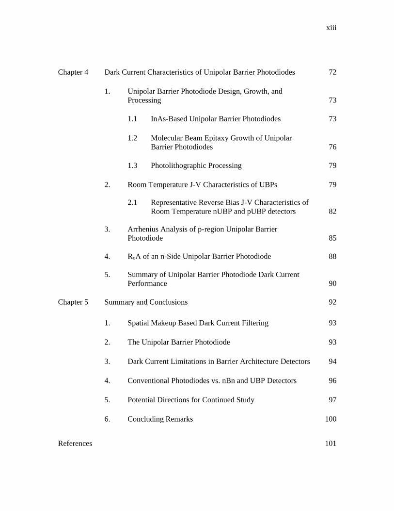
Table of Contents
Chapter 1 Introduction 1
1. Early Development of Mid-Wave Infrared Detectors 2
1.1 Alternatives to Compound Semiconductors 3
2. Typical Detector Architectures 3
2.1 The Simple Photoconductor 4
2.2 The pn Juction-Based Photodiode 5
3. Noise Generation in Infrared Detectors 6
3.1 Shot Noise 6
3.2 Other Detector Figures of Merit 7
3.2.1 The Zero Voltage Resistance-Area Product 7
3.2.2 Rule 07 8
4. Dark Current Mechanisms in Photodiodes and Related
Architectures 10
4.1 Surface Leakage Current 11
4.2 Generation Processes in Quasi-Neutral Regions 13
4.2.1 Auger Generation 14
4.2.2 Radiative Generation 16
4.2.3 Shockley-Read-Hall Generation 17
4.3 Generation Processes in Space Charge Regions 18
4.3.1 Shockley-Read-Hall Generation in the
Depletion Region 18
4.3.2 Trap-Assisted Tunneling 20
Page 11
xi
4.3.3 Direct Band-to-Band Tunneling 21
5. The Unipolar Barrier 22
5.1 Graded Unipolar Barriers 24
6. The nBn Detector 25
Chapter 2 Diffusion Current Characteristics in nBn Architecture Detectors 28
1. Diffusion of Carriers in Quasi-Neutral Regions 29
1.1 Long Diffusion Length Limited Carrier Diffusion 31
1.2 Short Diffusion Length Limited Carrier Diffusion 32
2. Auger Generated Diffusion Current 34
2.1 Long Diffusion Length Limited Auger Current 35
2.2 Short Diffusion Length Limited Auger Current 36
3. Neutral Region Shockley-Read-Hall Generated
Diffusion Current 37
3.1 Long Diffusion Length Neutral Region
SRH Current 37
3.2 Short Diffusion Length Neutral Region
SRH Current 38
4. The Effect of Donor Concentration on Dark Current
Characteristics 39
5. The Effect of Neutral Region SRH Generation on
nBn Performance 41
6. Experimental Evidence of Neutral Region SRH
Generation in nBn Detetors 44
Page 12
xii
6.1 Performance of SRH Limited nBns and
Conventional Photodiodes 48
6.2 RoA as it relates to the nBn Detector 49
Chapter 3 Dark Current Filtering via Unipolar Barrier-Based
Device Architectures 52
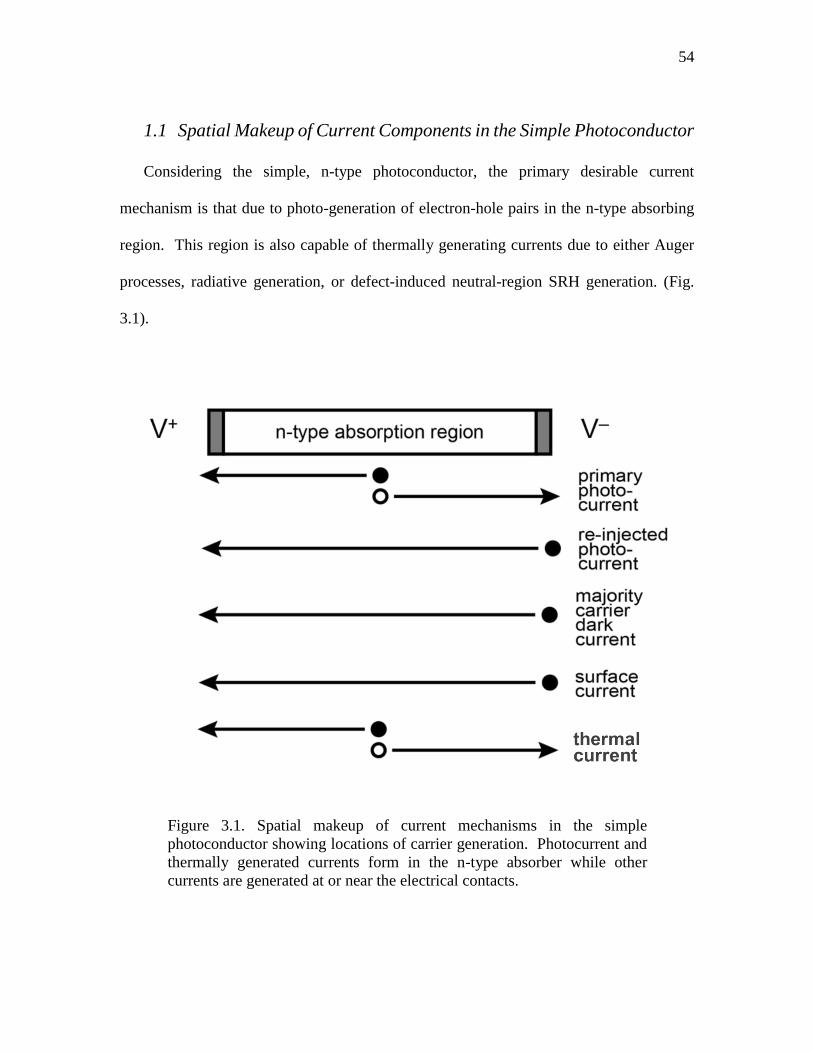
1. Spatial Makeup of Current Components in Photodetectors 53
1.1 Spatial Makeup of Current Components in the
Simple Photoconductor 54
1.2 Spatial Makeup of Current Components in the
Conventional Photodiode 55
2. Current Filtering via Unipolar Barriers 57
2.1 Current Filtering in the nBn Detector 58
3. The Unipolar Barrier Photodiode 60
3.1 p-Region Unipolar Barrier Photodiode 62
3.1.1 Current Filtering in the p-Region
Unipolar Barrier Photodiode 63
3.2 n-Region Unipolar Barrier Photodiode 65
3.2.1 Current Filtering in the n-Region
Unipolar Barrier Photodiode 66
4. Advantages and Limitations of Unipolar Barrier
Architectures 68
4.1 Advantages of Unipolar Barrier-Based Epitaxial
Architectures 69
4.2 Limitations of Unipolar Barrier-Based Epitaxial
Architectures 70
Page 13
xiii
Chapter 4 Dark Current Characteristics of Unipolar Barrier Photodiodes 72
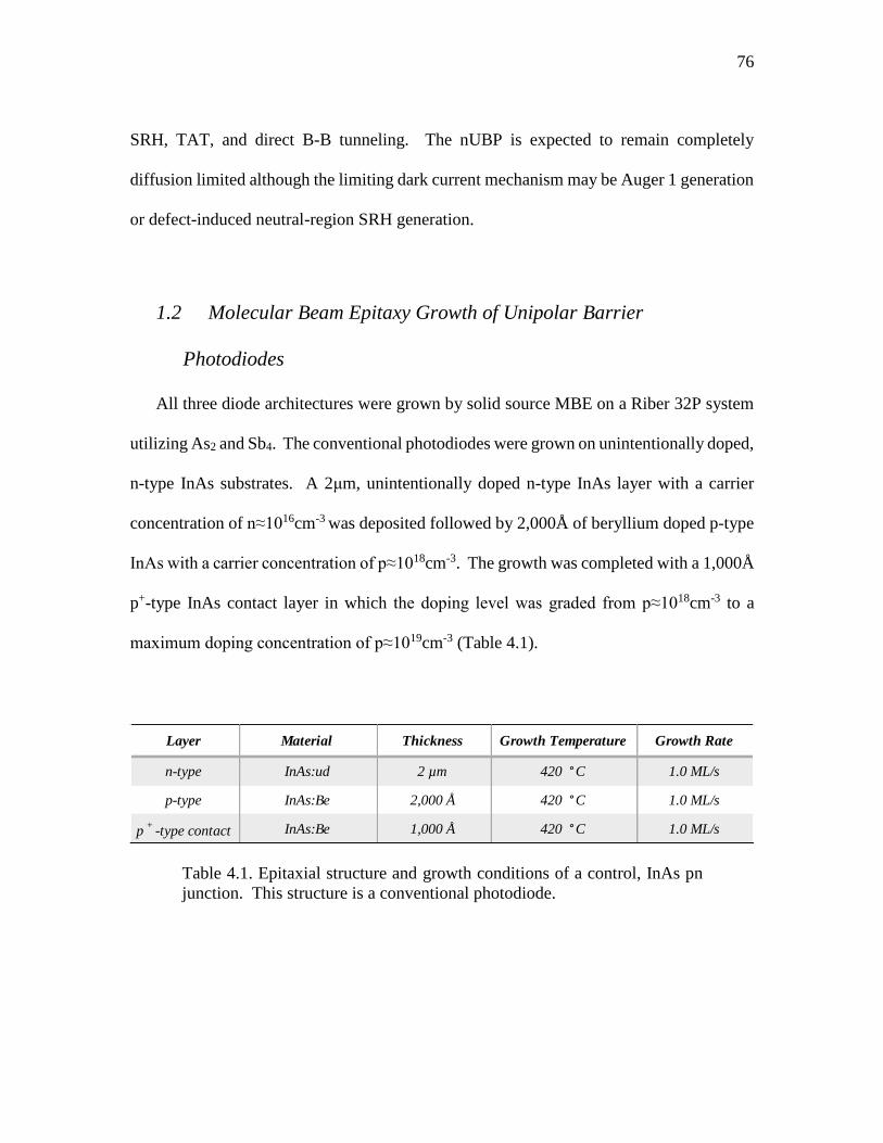
1. Unipolar Barrier Photodiode Design, Growth, and
Processing 73
1.1 InAs-Based Unipolar Barrier Photodiodes 73
1.2 Molecular Beam Epitaxy Growth of Unipolar
Barrier Photodiodes 76
1.3 Photolithographic Processing 79
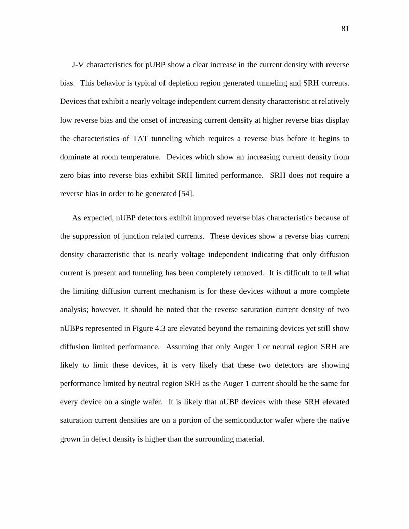
2. Room Temperature J-V Characteristics of UBPs 79
2.1 Representative Reverse Bias J-V Characteristics of
Room Temperature nUBP and pUBP detectors 82
3. Arrhenius Analysis of p-region Unipolar Barrier
Photodiode 85
4. RoA of an n-Side Unipolar Barrier Photodiode 88
5. Summary of Unipolar Barrier Photodiode Dark Current
Performance 90
Chapter 5 Summary and Conclusions 92
1. Spatial Makeup Based Dark Current Filtering 93
2. The Unipolar Barrier Photodiode 93
3. Dark Current Limitations in Barrier Architecture Detectors 94
4. Conventional Photodiodes vs. nBn and UBP Detectors 96
5. Potential Directions for Continued Study 97
6. Concluding Remarks 100
References 101
Page 14
xiv
List of Tables
Table Title Page
Table 4.1 Epitaxial growth parameters for an InAs-based pn junction 76
Table 4.2 Epitaxial growth parameters for an InAs-based p-region
unipolar barrier photodiode 77
Table 4.3 Epitaxial growth parameters for an InAs-based n-region
unipolar barrier photodiode 78
Page 15
xv
List of Figures
Figure Title Page
Figure 1.1 Bulk band diagram of a simple photoconductor 4
Figure 1.2 Bulk band diagram of a conventional photodiode 5
Figure 1.3 Surface leakage shunt path on a pn junction 11
Figure 1.4 Surface Fermi level pinning in InAs 12
Figure 1.5 Diffusion of carriers in a photodiode 14
Figure 1.6 Auger 1 and Auger 7 generation processes 15
Figure 1.7 The radiative generation process 16
Figure 1.8 The Shockley-Read-Hall generation process 17
Figure 1.9 Depletion region Shockley-Read-Hall process 19
Figure 1.10 The trap-assisted tunneling process 20
Figure 1.11 Direct band-to-band tunneling compared to trap-assisted tunneling 21
Figure 1.12 Majority and minority carrier unipolar barriers 23
Figure 1.13 Graded minority carrier unipolar barriers 24
Figure 1.14 Bulk band diagram of an nBn detector 26
Page 16
xvi
Figure 2.1 Long diffusion length limit in an nBn detector 31
Figure 2.2 Short diffusion length limit in an nBn detector 33
Figure 2.3 Dark current density versus donor concentration for a typical nBn 40
Figure 2.4 Dark current versus defect concentration for a typical nBn 41
Figure 2.5 Dark current versus proton fluence for an irradiated nBn 45
Figure 2.6 Arrhenius plot for lattice matched and mismatched nBn detectors 47
Figure 2.7 Arrhenius plot for defect limited nBn and conventional photodiode 48
Figure 2.8 Reverse bias current characteristics for defect-limited nBn detectors 50
Figure 3.1 Spatial makeup of currents in the simple photoconductor 54
Figure 3.2 Spatial makeup of currents in the conventional photodiode 56
Figure 3.3 Effect of poor unipolar barrier placement in an nBn detector 58
Figure 3.4 Current filtering in an ideal nBn detector 59
Figure 3.5 Effect of poor barrier placement in a unipolar barrier photodiode 61
Figure 3.6 Bulk band diagram of a p-region unipolar barrier photodiode 62
Figure 3.7 Current filtering in a p-region unipolar barrier photodiode 64
Figure 3.8 Current generation in a p-region unipolar barrier photodiode 65
Figure 3.9 Bulk band diagram of an n-region unipolar barrier photodiode 66
Page 17
xvii
Figure 3.10 Current filtering in an n-region unipolar barrier photodiode 67
Figure 3.11 Current generation in an n-region unipolar barrier photodiode 68
Figure 3.12 The graded barrier, p-region unipolar barrier photodiode 71
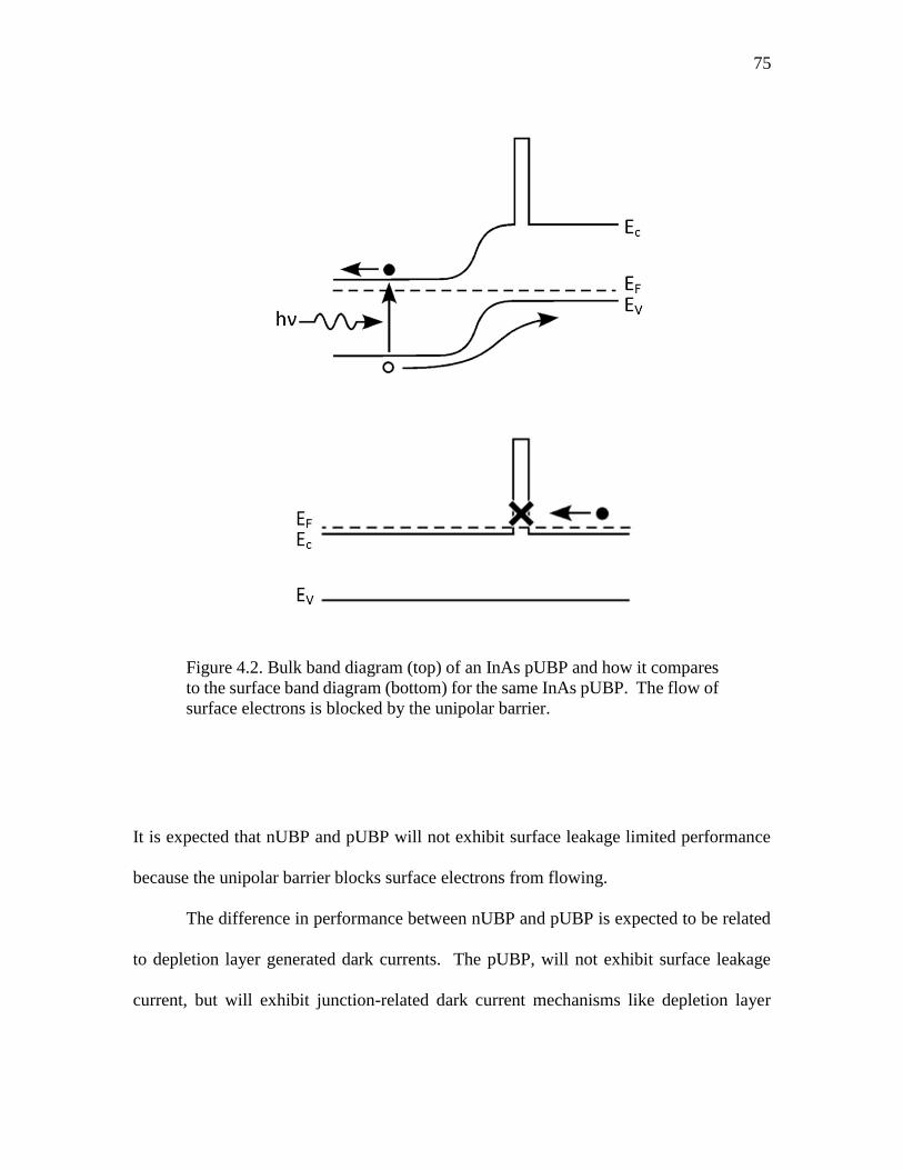
Figure 4.1 Bulk and surface band diagram of an InAs pn junction 74
Figure 4.2 Bulk and surface band diagram of an InAs p-region
unipolar barrier photodiode 75
Figure 4.3 Room temperature current density-voltage characteristics of
InAs unipolar barrier photodiodes 80
Figure 4.4 Dark current fitting for characteristic current density-voltage
characteristics for InAs unipolar barrier photodiodes 84
Figure 4.5 Representative current-density voltage characteristics for an
InAs conventional photodiode and p-region unipolar barrier
photodiode 86
Figure 4.6 Dark current density Arrhenius plot for an InAs, p-region unipolar
barrier photodiode and conventional photodiode 87
Figure 4.7 RoA Arrhenius plot for an InAs, n-region unipolar barrier
photodiode and conventional photodiode 89
Page 18
xviii
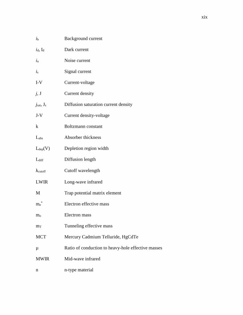
List of Symbols
B-B, BB Band-to-band
CMOS Complimentary metal-oxide semiconductor
Dp Diffusion coefficient for minority carrier holes
e Charge of the electron
EC Conduction band energy
EF Fermi energy
Eg Bandgap energy
Et Trap energy
EV Valence band energy
εs Static dielectric constant
∆f Frequency bandwidth
F(V) Electric field
F1,F2 Electron wave function overlap integrals
FPA Focal plane array
G-R Generation-recombination
ħ Planck’s constant
i Intrinsic material
I Current
Page 19
xix
ib Background current
id, Id Dark current
in Noise current
is Signal current
I-V Current-voltage
j, J Current density
jsat, Js Diffusion saturation current density
J-V Current density-voltage
k Boltzmann constant
Labs Absorber thickness
Ldep(V) Depletion region width
Ldiff Diffusion length
λcutoff Cutoff wavelength
LWIR Long-wave infrared
M Trap potential matrix element
me* Electron effective mass
mo Electron mass
mT Tunneling effective mass
MCT Mercury Cadmium Telluride, HgCdTe
µ Ratio of conduction to heavy-hole effective masses
MWIR Mid-wave infrared
n n-type material
Page 20
xx
ni Intrinsic carrier concentration
nBn n-type, unipolar barrier, n-type
Ndefect Defect density, defect concentration
Ndonor, Nd Donor density, donor concentration
NT Trap density
nUBP n-region unipolar barrier photodiode
p p-type material
pUBP p-region unipolar barrier photodiode
Φ Proton fluence
RHEED Reflection high-energy electron diffraction
RoA Zero bias resistance-area product
s Surface recombination velocity
σ Defect capture cross section
SNR Signal-to-noise ratio
SRH Shockley-Read-Hall
T Temperature
τ, τo Minority carrier lifetime
τA1 Auger 1 lifetime
τiA1 Auger 1 lifetime in intrinsic material
τSRH Shockley-Read-Hall lifetime
TAT Trap-assisted tunneling
UBP Unipolar barrier photodiode
Page 21
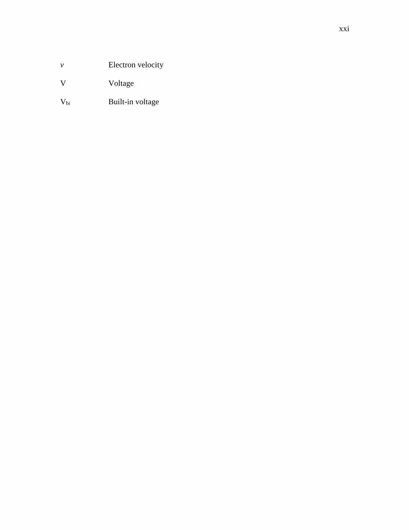
xxi
v Electron velocity
V Voltage
Vbi Built-in voltage
Page 22
1
Chapter 1
Introduction
The detection of optical signals continues to be an area of fervent research.
Improving performance of and understanding the underlying physics limiting existing
technologies is as important as the development of new techniques and device architectures
for enhanced optical detection. Detectors and specifically focal plane arrays (FPAs)
operating in the mid-wave infrared (MWIR) and the long-wave infrared (LWIR) bands,
covering wavelength ranges of 3-5µm and 8-12µm respectively, are of particular interest.
The MWIR and LWIR bands are valuable for a wide range of civilian and military
applications including aerial firefighting, ground-based night vision, target acquisition, and
space-based imaging and sensing [1]. Significant efforts have been made towards lowering
the cost and improving performance of optical detectors operating in the infrared spectrum,
but there remains substantial room for improvement.
The current state of the art for optical detection in the MWIR bands utilizes
compound semiconductors in the II-VI family of materials, specifically Mercury Cadmium
Telluride (MCT) as the light-absorbing material [2]. This material family presents many
challenges for building efficient detectors including expensive and fragile materials, the
need for effective surface passivation, CMOS integration, limited radiation tolerance, and
stringent cooling requirements [3, 4]. Recent research efforts have focused on alleviating
Page 23
2
these limitations via novel epitaxial structures and utilization of the comparably less limited
III-V compound semiconductor family; however, realizing efficient, high performance
detection in the MWIR spectrum using III-V materials presents a new and unique set of
challenges.
1. Early Development of Mid-Wave Infrared Detectors
Although the existence of infrared radiation has been known for much longer, MWIR
and LWIR detection has only been studied in detail since the 1950s. Initially, cooled,
polycrystalline lead salts were the material of choice, but material quality, and thus efficacy
of detection did not improve until after the advent of the transistor and improved material
quality [5]. Late in the 1950s, the III-V and then II-VI semiconductor material systems
were introduced leading to a large increase in materials available for infrared detection
including InSb, InAs, and MCT [6, 7]. Of these materials, MCT boasted an exceptionally
large range of cutoff wavelengths with virtually negligible change in lattice constant across
the compositional range of the ternary [8]. For these reasons, MCT has been extensively
studied over the last 50 years and is an extremely mature material by compound
semiconductor standards [9].
Relatively recently, the emergence of short-period, strained-layer superlattices for
bandgap engineering as well as advanced epitaxial structures based on the unipolar barrier
have given rise to a new push in the development of infrared detectors in the III-V materials
Page 24
3
family [10-12]. This thrust is currently receiving a significant amount of research attention
and is the motivation for this work.
1.1 Alternatives to Compound Semiconductors
Although photon detection via compound semiconductors produces the highest level
of performance for infrared detectors, compound semiconductors are not the only materials
available for detection of infrared radiation. Thermal detection of infrared energy can be
accomplished by thermopile, pyroelectric, or bolometer detectors [13, 14]. Of these
detector types, bolometers, which utilize a material with a temperature dependent
resistance, provide the highest level of performance. Microbolometer arrays with either
vanadium oxide or amorphous silicon absorbers are a typical for low cost infrared imaging
systems [15]. New materials are currently being studied as potential competitors for high
performance infrared imaging, most notably, graphene due to its high material quality and
advantageous electrical properties [16].
2. Typical Detector Architectures
Until recently, there were primarily two device architectures upon which the majority
of semiconductor-based MWIR photon detectors were built. These are the simple
photoconductor and the pn junction-based photodiode. Each architecture exhibits a unique
Page 25
4
set of current-voltage characteristics and is subject to a different set of dark current
mechanisms, which may limit overall device performance.
2.1 The Simple Photoconductor
Photoconductive detectors, in their most basic form, are comprised of a single material
type, usually n-type. These detectors require an applied bias to operate with photodetection
occurring through a change in conductivity caused by light absorbed in the material.
Photoconductors are generally limited either by background current which is unwanted
photocurrent generated by the thermal background radiation or by the flow of majority
carriers from metal contact to contact (Fig. 1.1) [17].
Figure 1.1. Photoconductive detectors are generally limited by majority
carrier flow from top-side metal contact, through the semiconductor
material, and finally to the back-side metal contact.
The metal-semiconductor contacts are ohmic, presenting no barriers to impede the flow of
these majority carriers between the contacts, thus this flow is a significant source of dark
current in photoconductive detectors.
Page 26
5
2.2 The pn Junction-Based Photodiode
The photodiode is a photovoltaic detector based on the standard pn junction and
generally does not require an applied bias voltage in order to detect light. Photo-generated
carriers may manifest in any part of the device, although typically, the majority of
photoexcitation will occur in a predetermined absorbing region as shown in Figure 1.2.
The conductivity of this absorbing region may be p-type or n-type [18].
Figure 1.2. Bulk band diagram of a conventional photodiode. Unlike the
simple photoconductor, the pn junction-based photodiode has a built in
barrier which blocks the flow of majority carriers from contact to contact.
The pn junction blocks the majority current that is the main source of dark current of
photoconductors, but has several dark current mechanisms that affect it. These detectors
may be limited by the same background current possible in photoconductive detectors, or
they may be limited by surface leakage current or bulk related dark currents [19].
Page 27
6
3. Noise Generation in Infrared Detectors
Ultimately, the signal-to-noise ratio (SNR) is considered the best judge of a
photodetector’s performance. The SNR can be described in terms of the electrical current
generated by desirable photo-generated carriers, the signal, and the current due to noise in
the device:
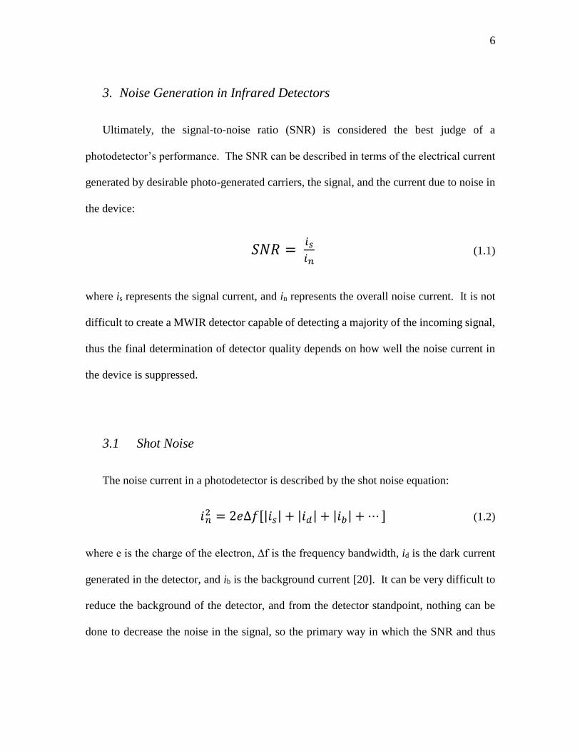
𝑆𝑁𝑅 = 𝑖𝑠
𝑖𝑛 (1.1)
where is represents the signal current, and in represents the overall noise current. It is not
difficult to create a MWIR detector capable of detecting a majority of the incoming signal,
thus the final determination of detector quality depends on how well the noise current in
the device is suppressed.
3.1 Shot Noise
The noise current in a photodetector is described by the shot noise equation:
𝑖𝑛2 = 2𝑒∆𝑓[|𝑖𝑠| + |𝑖𝑑| + |𝑖𝑏| + ⋯ ] (1.2)
where e is the charge of the electron, ∆f is the frequency bandwidth, id is the dark current
generated in the detector, and ib is the background current [20]. It can be very difficult to
reduce the background of the detector, and from the detector standpoint, nothing can be
done to decrease the noise in the signal, so the primary way in which the SNR and thus
Page 28
7
detector performance can be improved is by reducing the dark current, id, to a level less
than that of the next highest current, typically either is or ib.
3.2 Other Detector Figures of Merit
Besides the SNR, there are many detector figures of merit that are used regularly for
infrared detectors. Two in particular, the zero voltage resistance-area product, RoA, and
Rule 07 are described here as they are of particular importance to MWIR and LWIR
detectors and the work presented henceforth.
3.2.1 The Zero Voltage Resistance-Area Product
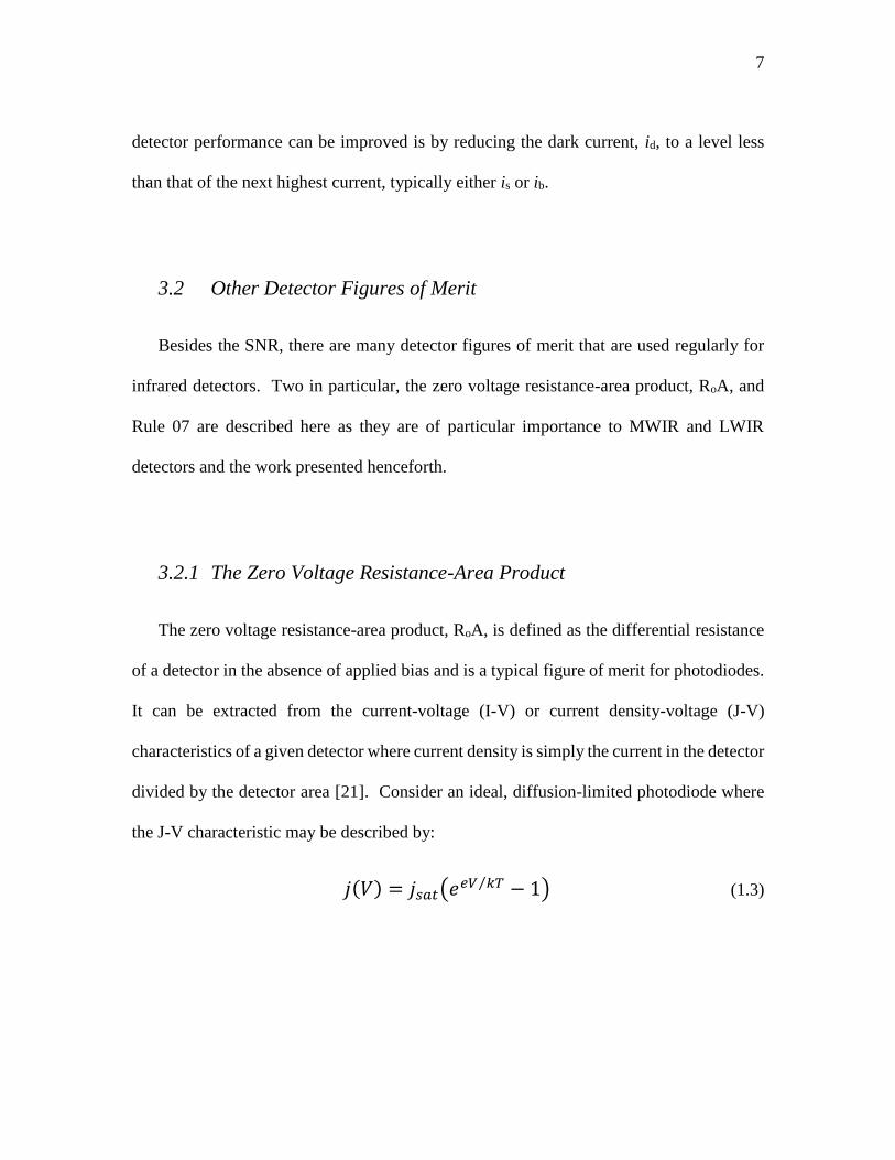
The zero voltage resistance-area product, RoA, is defined as the differential resistance
of a detector in the absence of applied bias and is a typical figure of merit for photodiodes.
It can be extracted from the current-voltage (I-V) or current density-voltage (J-V)
characteristics of a given detector where current density is simply the current in the detector
divided by the detector area [21]. Consider an ideal, diffusion-limited photodiode where
the J-V characteristic may be described by:
𝑗(𝑉) = 𝑗𝑠𝑎𝑡(𝑒𝑒𝑉 𝑘𝑇⁄ − 1) (1.3)
Page 29
8
where jsat is defined as the diffusion saturation current density, V is the applied voltage, T
is the temperature of the photodiode, and k is the Boltzmann constant [18]. The RoA for
such a detector is then defined by:
𝑅𝑜𝐴 = (𝑑𝑗
𝑑𝑉)
|𝑉=0
−1=
𝑘𝑇
𝑒𝑗𝑠𝑎𝑡 (1.4)
There is an inverse proportionality between RoA and the saturation current density due to
diffusion, jsat. An increase in the dark current manifests as an increase in the saturation
current for diffusion-limited processes, thus increasing dark currents reduces the RoA while
decreasing dark currents will result in a larger RoA value.
It also turns out that non-diffusion related processes, those noise mechanisms generated
in the depletion region of the photodiode as well as surface leakage currents, will negatively
influence the RoA in the same way as diffusion related processes making this a robust
figure of merit for photodiodes [22].
3.2.2 Rule 07
Rule 07 is an empirical metric for MWIR and LWIR detectors. It was determined in
2007 utilizing the highest performance, state-of-the-art MCT detectors, still the highest
performing infrared detectors to date. The rule gives the current density for high
performance detectors with a given cutoff wavelength, λcutoff, at a given temperature. The
rule is described by [23]:
Page 30
9
𝑗 = 𝑗𝑠𝑎𝑡𝑒−1.16239134096245(1.24𝑒 𝑘𝜆𝑒𝑇)⁄ (1.5)
where,
𝜆𝑒 = 𝜆𝑐𝑢𝑡𝑜𝑓𝑓 for 𝜆𝑐𝑢𝑡𝑜𝑓𝑓 ≥ 4.63513642316149 𝜇𝑚
and
𝜆𝑒 =𝜆𝑐𝑢𝑡𝑜𝑓𝑓
[1 − (0.200847413564122 𝜇𝑚
𝜆𝑐𝑢𝑡𝑜𝑓𝑓−
0.200847413564122 𝜇𝑚4.63513642316149 𝜇𝑚
)0.544071281108481
]
for 𝜆𝑐𝑢𝑡𝑜𝑓𝑓 < 4.63513642316149 𝜇𝑚 (1.6)
In concept, any detector with performance matching that described by Rule 07 is operating
at the current state-of-the-art. Any detector exhibiting a dark current in excess of Rule 07
will have greater noise generation than the highest quality detectors. To date, no detector
has surpassed Rule 07, but in the event a detector is created which shows a current less
than that described by Rule 07, that detector will represent the new state-of-the-art for
MWIR or LWIR detection.
Rule 07 was revisited in 2009. It was determined that Rule 07 very nearly describes
the limits imposed by Auger 1 generation in n-type MCT [24]. Auger processes will be
described later in this chapter and in greater detail in chapter 2. Performance on or very
near the Rule 07 line can be seen as an indication of Auger-limited or near Auger-limited
performance. As Auger generation is determined by fundamental material properties rather
than the presence of defects, Auger-limited performance is often considered the ultimate
limit to infrared detector performance.
Page 31
10
4. Dark Current Mechanisms in Photodiodes and Related Architectures
There are many possible sources of dark currents in MWIR detectors. They can be
classified by the location in the device architecture in which a given dark current
mechanism is generated: either at the surface of the semiconductor, in the quasi-neutral
regions, or in depletion layers as the device architecture allows. Furthermore, these noise
generating, dark current mechanisms can be caused by defects or by native material
properties and may be subject primarily to carrier drift, or carrier diffusion.
Elevated defect concentrations are a particularly significant problem for MWIR
detectors as the introduction of defects typically increases dark currents and decreases the
quantum efficiency [19]. There are several possible sources of defects in compound
semiconductor-based detectors. In some cases, defects can be grown into the structure
either as defects directly grown into the bulk crystal lattice, dislocations from growth on
mismatched substrates, or layer interface defects in type-II strained layer superlattices [25-
27]. In some applications for MWIR detection, devices may operate in environments in
which exposure to radiation is a concern. In this case, even a high performance detector
may become severely defect limited as irradiation causes a significant reduction in
performance [28]. As elevated dark currents will increase noise in the detector, it is
important to understand the impact elevated defect concentrations will have on detector
performance.
Page 32
11
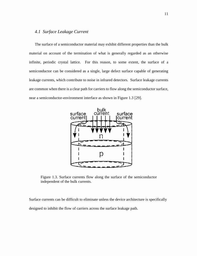
4.1 Surface Leakage Current
The surface of a semiconductor material may exhibit different properties than the bulk
material on account of the termination of what is generally regarded as an otherwise
infinite, periodic crystal lattice. For this reason, to some extent, the surface of a
semiconductor can be considered as a single, large defect surface capable of generating
leakage currents, which contribute to noise in infrared detectors. Surface leakage currents
are common when there is a clear path for carriers to flow along the semiconductor surface,
near a semiconductor-environment interface as shown in Figure 1.3 [29].
Figure 1.3. Surface currents flow along the surface of the semiconductor
independent of the bulk currents.
Surface currents can be difficult to eliminate unless the device architecture is specifically
designed to inhibit the flow of carriers across the surface leakage path.
Page 33
12
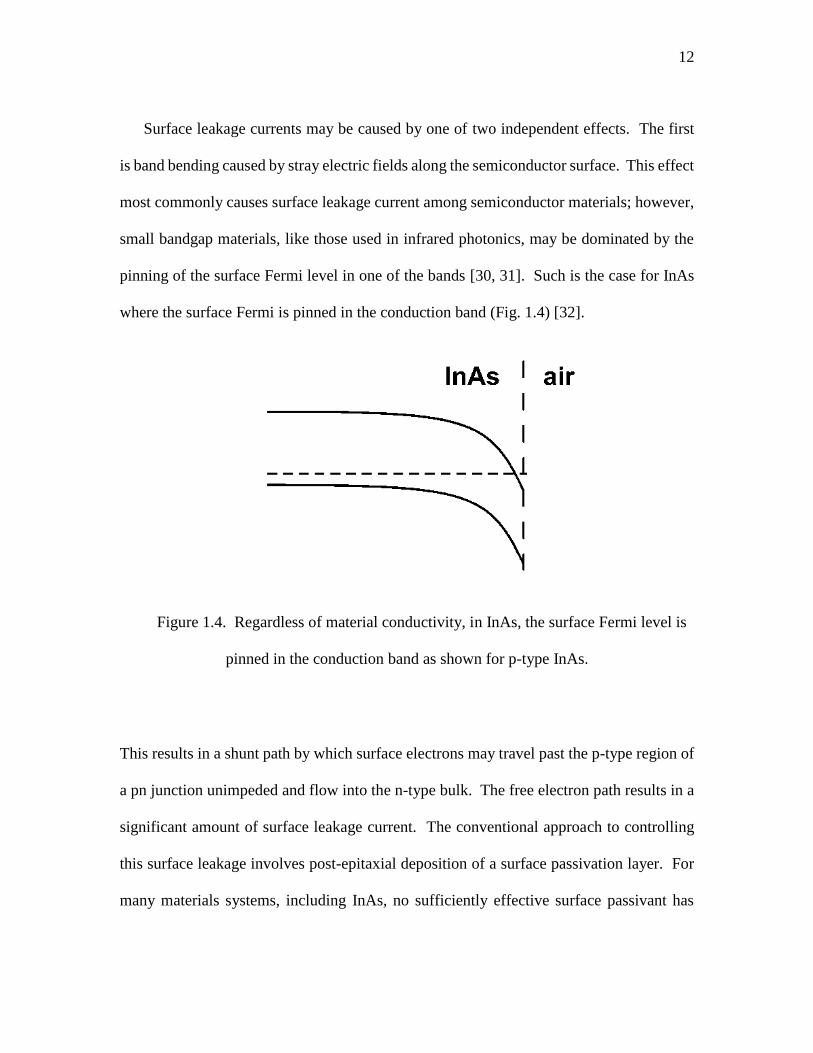
Surface leakage currents may be caused by one of two independent effects. The first
is band bending caused by stray electric fields along the semiconductor surface. This effect
most commonly causes surface leakage current among semiconductor materials; however,
small bandgap materials, like those used in infrared photonics, may be dominated by the
pinning of the surface Fermi level in one of the bands [30, 31]. Such is the case for InAs
where the surface Fermi is pinned in the conduction band (Fig. 1.4) [32].
Figure 1.4. Regardless of material conductivity, in InAs, the surface Fermi level is
pinned in the conduction band as shown for p-type InAs.
This results in a shunt path by which surface electrons may travel past the p-type region of
a pn junction unimpeded and flow into the n-type bulk. The free electron path results in a
significant amount of surface leakage current. The conventional approach to controlling
this surface leakage involves post-epitaxial deposition of a surface passivation layer. For
many materials systems, including InAs, no sufficiently effective surface passivant has
Page 34
13
been found. As a result, surface leakage current may be reduced using surface passivation,
but may still be the limiting current mechanism [33]. Furthermore, generating the surface
passivation layer is costly and time consuming, so an alternative to surface passivation is,
therefore, desirable.
4.2 Generation Processes in Quasi-Neutral Regions
Dark currents may be generated in quasi-neutral regions of a detector. A quasi-neutral
region exists in either n-type, p-type, or intrinsic material wherever there is no space charge
region present. Absorbing regions of photoconductors and photodiodes, with the exception
of p-i-n architecture detectors, are typically considered to be quasi-neutral. In these
regions, carriers that are generated must diffuse to the contacts or the space charge region
if the detector is based on a pn junction. It should be noted that carrier diffusion is a
different process than that of carrier drift caused by the electric field in a depletion layer
and thus diffusion-limited dark currents typically exhibit different characteristics than drift-
related dark current mechanisms [19].
Carriers may be generated in quasi-neutral regions via thermal excitation across the
bandgap, thermal excitation through trap states within the bandgap, or via radiative
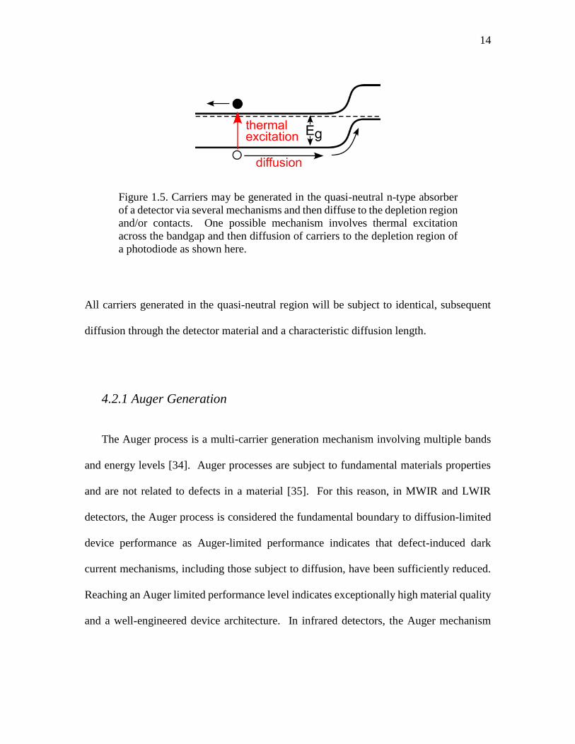
processes (Fig. 1.5)
Page 35
14
Figure 1.5. Carriers may be generated in the quasi-neutral n-type absorber
of a detector via several mechanisms and then diffuse to the depletion region
and/or contacts. One possible mechanism involves thermal excitation
across the bandgap and then diffusion of carriers to the depletion region of
a photodiode as shown here.
All carriers generated in the quasi-neutral region will be subject to identical, subsequent
diffusion through the detector material and a characteristic diffusion length.
4.2.1 Auger Generation
The Auger process is a multi-carrier generation mechanism involving multiple bands
and energy levels [34]. Auger processes are subject to fundamental materials properties
and are not related to defects in a material [35]. For this reason, in MWIR and LWIR
detectors, the Auger process is considered the fundamental boundary to diffusion-limited
device performance as Auger-limited performance indicates that defect-induced dark
current mechanisms, including those subject to diffusion, have been sufficiently reduced.
Reaching an Auger limited performance level indicates exceptionally high material quality
and a well-engineered device architecture. In infrared detectors, the Auger mechanism
Page 36
15
involves the thermal generation of carriers with an energy of at least the bandgap as shown
in Figure 1.6.
Figure 1.6. The Auger 1 (left) and 7 (right) generation processes. Auger 1
and 7 are expected to dominate in n-type and p-type material respectively.
Auger processes in MWIR detectors manifest via thermal generation of
carriers.
The Auger 1 process tends to be the limiting Auger generation mechanism in n-type
material, while Auger 7 typically limits Auger generation in p-type material. It is generally
the case that Auger 7 is a smaller effect than Auger 1, thus a p-type material-based
photodetector architecture will likely exhibit a fundamentally higher level of performance
than one based primarily on n-type material in the absorber [24].
Page 37
16
4.2.2 Radiative Generation
Radiative generation as it relates to dark current occurs in direct bandgap materials
when photons emitted due to the thermal energy of the material itself are reabsorbed within
the material resulting in the creation of an electron hole pair (Fig. 1.7) [36].
Figure 1.7. Radiative generation occurs when a thermally generated photon
is reabsorbed by the semiconductor material. Radiative generation lifetimes
are expected to be very long in most MWIR detectors.
Radiative lifetimes in narrow bandgap materials tend to be very long compared to Auger
lifetimes, thus radiative generation is typically not an important consideration for infrared
detection unless the detector operates at short wavelengths and very low temperatures [19].
Page 38
17
4.2.3 Shockley-Read-Hall Generation
Shockley-Read-Hall (SRH) or generation-recombination (G-R) currents are a well
understood effect in semiconductors. SRH currents arise via thermal generation through
trap (defect) states located throughout the bandgap of a material (Fig. 1.8) [37, 38].
Figure 1.8. Shockley-Read-Hall generation in a neutral region. In SRH
processes, carriers are generated or recombine via defect-induced trap states
within the bandgap. In principle, trap states can exist throughout the
bandgap.
SRH current may be generated in quasi-neutral regions as described in detail in chapter 2
or in depletion regions as described later in this chapter. Depletion region SRH is typically
a much larger effect than SRH in a quasi-neutral region and a significant limitation to pn
junction performance [39]. Only relatively recently have high-performance, infrared
detector device architectures capable of significantly suppressing depletion region SRH
been created, thus the effects of SRH on neutral regions has received very little attention
nor experimental observation and qualification until now.
Page 39
18
4.3 Generation Processes in Space Charge Regions
Space charge, or depletion, regions are subject to the effects of a built in electric field
induced by the movement of charge carriers across a material junction and are typically
associated with pn junctions. The electric field results in carrier drift, thus carriers
generated in the space charge region of a photodiode are propelled away from the depletion
region at a rate greater than that imposed by diffusion in quasi-neutral material [18]. There
are several dark current mechanisms that may generate in the depletion layer of a pn
junction based photodiode. Typically, the limiting dark current mechanism generated in
the depletion region will be induced by trap states in the bandgap caused by material
defects, tunneling of carriers, or both.
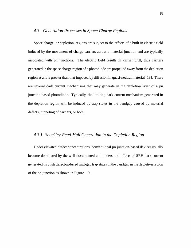
4.3.1 Shockley-Read-Hall Generation in the Depletion Region
Under elevated defect concentrations, conventional pn junction-based devices usually
become dominated by the well documented and understood effects of SRH dark current
generated through defect-induced mid-gap trap states in the bandgap in the depletion region
of the pn junction as shown in Figure 1.9.
Page 40
19
Figure 1.9. In a typical photodiode, Shockley-Read-Hall generation occurs
most efficiently through mid-gap defect states in the depletion layer of the
pn junction. Under reverse bias, carriers are thermally generated through
the defect states.
Carriers generated via depletion region SRH are subject primarily to carrier drift due to the
built in electric field rather than diffusion of carriers. Such defect-limited pn junctions
exhibit SRH dark current that decreases with temperature and an activation energy of one-
half of the bandgap and increases in proportion to the defect density as described by
Shockley’s theory. The reverse saturation current density for this mechanism is given by:
𝐽𝑑−𝑆𝑅𝐻 =𝑒𝑛𝑖(𝑇)𝐿𝑑𝑒𝑝(𝑉)
2𝜏𝑆𝑅𝐻
2𝑘𝑇
𝑒(𝑉𝑏𝑖 − 𝑉)𝑠𝑖𝑛ℎ (−
𝑒𝑉
2𝑘𝑇) ∫
𝑑𝑢
𝑢2 + 2𝑢𝑒−𝑒𝑉 2𝑘𝑇⁄ + 1
∞
0
(1.7)
where Ldep(V) is the width of the depletion region, τSRH is the minority carrier lifetime due
to the SRH process, and Vbi is the built-in voltage of the junction [37, 38]. At reverse
voltages larger than a few kT, the dominant temperature-dependence in equation 1.7 is
contained in the ni factor, where:
Page 41
20
𝑛𝑖(𝑇) ∝ 𝑒−𝐸𝑔 2𝑘𝑇⁄ (1.8)
is the intrinsic carrier concentration. As one typical way in which dark currents are reduced
in infrared detectors is via cooling of the detector, the half-bandgap activation energy
implied by the dependence of the intrinsic carrier concentration in equation 1.7 is a
significant limitation for defect-limited, conventional photodiodes.
4.3.2 Trap-Assisted Tunneling
Trap-assisted tunneling (TAT) arises when defect trap states are present in the depletion
layer or in the quasi-neutral region surrounding the depletion layer. Carriers may tunnel
through an occupied trap state into the other side of the junction and then flow freely
resulting in an increase in the dark current (Fig. 1.10) [40, 41].
Figure 1.10. Trap-assisted tunneling occurs even under low reverse bias in
a photodiode. Carriers are thermally generated from the valence band into
trap states and then tunnel from the trap state, through the space charge
region, and into the conduction band.
Page 42
21
TAT may occur at any bias voltage, thus control of TAT is critical. Improving the quality
of materials growth will lower the density of trap states and thereby reduce TAT, but this
may not always be a viable option. This is particularly true in the case of large FPAs when
device-to-device variation greatly affects the overall performance of the array.
4.3.3 Direct Band-to-Band Tunneling
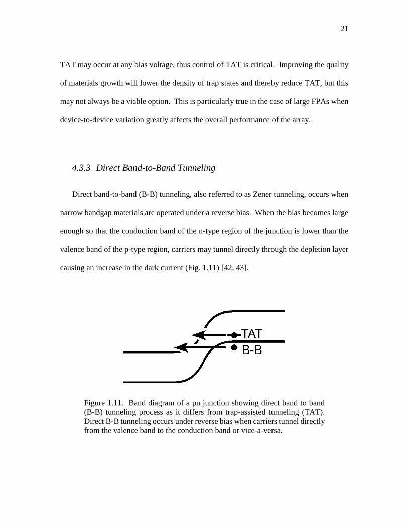
Direct band-to-band (B-B) tunneling, also referred to as Zener tunneling, occurs when
narrow bandgap materials are operated under a reverse bias. When the bias becomes large
enough so that the conduction band of the n-type region of the junction is lower than the
valence band of the p-type region, carriers may tunnel directly through the depletion layer
causing an increase in the dark current (Fig. 1.11) [42, 43].
Figure 1.11. Band diagram of a pn junction showing direct band to band
(B-B) tunneling process as it differs from trap-assisted tunneling (TAT).
Direct B-B tunneling occurs under reverse bias when carriers tunnel directly
from the valence band to the conduction band or vice-a-versa.
Page 43
22
Direct B-B tunneling differs from TAT in the reverse bias requirement and that it may
occur without the assistance of defect states, thus it is not a defect-induced dark current but
rather a consequence of material properties, applied bias, and device architecture. For this
reason, it can be difficult to impede direct B-B tunneling in a narrow bandgap material.
Direct B-B tunneling becomes more pronounced as the bandgap of the material
decreases, thus band-to-band tunneling is a more prominent problem for longer wavelength
infrared devices. This effect requires that devices in the MCT materials system be operated
at a minimal reverse bias or no reverse bias voltage [19].
5. The Unipolar Barrier
A unipolar barrier is a heterostructure specifically designed so that one carrier type,
either electrons or holes and either minority or majority carriers, may flow unimpeded
while the other carrier type may not flow [11]. In this case, the unipolar barrier is
represented by a material with a large band offset relative to the surrounding material in
either the valence or conduction band for the blocking of one carrier, but a zero band offset
condition in the other so the opposite carrier may flow unimpeded. The unipolar barrier
may have a large valence band offset or a large conduction band offset with a zero band
offset condition in either band. Depending on the type of material into which the barrier is
placed, the unipolar barrier may act as a barrier to either the majority or minority carriers
(Fig. 1.12).
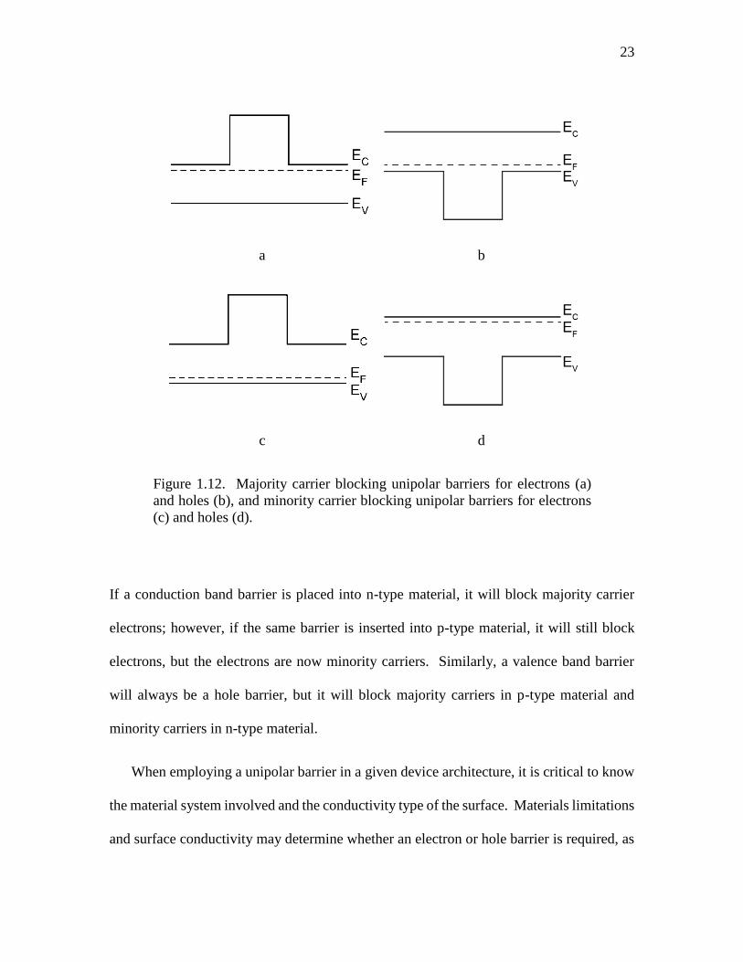
Page 44
23
a b
c d
Figure 1.12. Majority carrier blocking unipolar barriers for electrons (a)
and holes (b), and minority carrier blocking unipolar barriers for electrons
(c) and holes (d).
If a conduction band barrier is placed into n-type material, it will block majority carrier
electrons; however, if the same barrier is inserted into p-type material, it will still block
electrons, but the electrons are now minority carriers. Similarly, a valence band barrier
will always be a hole barrier, but it will block majority carriers in p-type material and
minority carriers in n-type material.
When employing a unipolar barrier in a given device architecture, it is critical to know
the material system involved and the conductivity type of the surface. Materials limitations
and surface conductivity may determine whether an electron or hole barrier is required, as
Page 45
24
well as the optimal location of the barrier. In addition to the requirement that the material
has a large offset in one band and no offset in the other, the material must be able to be
grown at a high quality and pseudomorphically.
5.1 Graded Unipolar Barriers
The above requirements of the heterojunction, namely zero-offset in one band, large
offset in the other band, and nearly lattice matched, are stringent and not available in most
materials systems. When a unipolar barrier is desired in such a system, a graded barrier
may be constructed by grading the bandgap from low to high and back to low while
maintaining constant doping as shown in Figure 1.13.
Figure 1.13. Graded minority carrier unipolar barriers in p-type (left) and
n-type (right) materials.
Page 46
25
The constant doping locks the majority carrier band into a flat condition, close to the flat
Fermi level, while the band on the other side of the bandgap from the Fermi level, the
minority carrier band, must rise up, as the bandgap increases, to produce a barrier via a
larger bandgap material. Thus, unipolar barriers formed by grading are always minority
carrier barriers but may be either electron-blocking barriers in p-type material or hole-
blocking barriers in n-type material.
6. The nBn Detector
The nBn detector was the first detector to utilize a unipolar barrier [11]. The device is
simply an n-type photoconductive detector with a majority-carrier electron-blocking
unipolar barrier inserted into the device structure. The barrier must be inserted into a
location in the device where it does not impede the flow of photo-generated current in the
absorbing layer (Fig. 1.14).
Page 47
26
Figure 1.14. Band diagram of the nBn detector. The barrier layer does not
impede the flow of photo-generated electrons, but allows photo-generated
holes to reach the contact on the right unimpeded. The barrier does,
however, effectively block the flow of majority carrier electrons and the
flow of surface electrons that would otherwise contribute to surface leakage
current.
The nBn naturally blocks surface leakage current and majority carrier electron flow from
the top to back-side ohmic contacts, resulting in a great improvement in performance and
a higher operating temperature compared to a simple photoconductor.
The device was first demonstrated with an InAs based detector. In the InAs
material system, AlAs0.18Sb0.82 has been identified as an ideal barrier material, as it is nearly
lattice matched to InAs while maintaining a zero valance band offset and a large conduction
band offset compared to InAs. InAs based nBn detectors have shown nearly six orders of
magnitude reduction in the dark current when compared to conventional InAs photodiodes,
and no detectable surface leakage current down to a temperature of 135K limited by
measurement capabilities, not device limitations [11, 44].
Page 48
27
Infrared detectors with the nBn architecture or related unipolar barrier architectures
perform differently under the presence of elevated defect concentrations when compared
to conventional pn-junction based photodiodes. Understanding this difference in
performance is critical to understanding the performance of current state-of-the-art nBn
detectors as well as the performance limitations of nBn detectors in general.
Page 49
28
Chapter 2
Diffusion Current Characteristics in nBn Architecture
Detectors
The nBn detector has shown considerable improvements in performance when
compared with the conventional, pn-junction based photodiode. The nBn architecture
naturally inhibits surface leakage current and direct flow of majority carriers that limit the
basic photoconductor. Furthermore, in the nBn, the depletion region is limited to a material
with a much larger bandgap than the absorber, so currents generated in the space charge
region of pn junctions, including depletion-layer SRH generation, TAT, and direct B-B
tunneling are reduced by many orders of magnitude and will not contribute to detector
noise in an observable way. However, the generation of minority carriers in the n-type,
quasi-neutral absorbing region of the nBn may limit performance by contributing to the
overall dark current and thus noise in the detector.
Electron-hole pairs may be generated in quasi-neutral regions of semiconductors via
several mechanisms. Under the correct conditions, these carriers may diffuse to the
electrical contacts and register as current or recombine if contacts are not within a diffusion
length of the location of carrier generation. This is the mechanism by which an incoming
optical signal is converted to a photocurrent; however, it is also a mechanism through
which dark currents can flow. Carriers can be generated via thermal excitation directly
Page 50
29
across the bandgap or via trap states within the bandgap of the material. Both of these
carrier generation processes will contribute to the dark current of the detector, but carrier
generation occurs primarily via two distinct mechanisms with differing current
characteristics.
1. Diffusion of Carriers in Quasi-Neutral Regions
The diffusion current characteristics of n-type quasi-neutral regions is well understood.
In general, this diffusion current density is given by:
𝐽 = 𝐽𝑆(𝑒𝑒𝑉 𝑘𝑇⁄ − 1) (2.1)
where JS is the reverse saturation current density, e is the charge of the electron, V is the
applied bias voltage, k is the Boltzmann constant, and T is the temperature of the detector
[22]. The value of JS is directly related to the dominant noise mechanism contributing to
diffusion related dark current in the n-type quasi-neutral region, thus understanding the
characteristics of the reverse saturation current density can provide insight into the
mechanism dominating the diffusion dark current. The general expression for JS in an n-
type quasi-neutral region independent of region thickness is:
𝐽𝑆 =𝑒𝑛𝑖
2𝐿𝑑𝑖𝑓𝑓
𝑁𝑑𝑜𝑛𝑜𝑟𝜏
𝛽+𝑡𝑎𝑛ℎ(𝐿𝑎𝑏𝑠
𝐿𝑑𝑖𝑓𝑓⁄ )
1+𝛽𝑡𝑎𝑛ℎ(𝐿𝑎𝑏𝑠
𝐿𝑑𝑖𝑓𝑓⁄ )
(2.2)
where,
Page 51
30
𝛽 =𝑆
𝐿𝑑𝑖𝑓𝑓 𝜏⁄ (2.3)
and where s is the surface recombination velocity, Ldiff is the minority carrier diffusion
length, Ndonor is the donor density, τ is the minority carrier lifetime, and Labs is the thickness
of the absorbing region [45].
Under the boundary condition requiring the current due to holes to be zero at the
interface of the substrate and the n-type quasi-neutral absorber, the β factor will go to zero,
and it can been shown that the diffusion saturation current density for a quasi-neutral n-
region is described by:
𝐽𝑆 =𝑒𝑛𝑖
2𝐿𝑑𝑖𝑓𝑓
𝑁𝑑𝑜𝑛𝑜𝑟𝜏𝑡𝑎𝑛ℎ (
𝐿𝑎𝑏𝑠𝐿𝑑𝑖𝑓𝑓
⁄ ) (2.4)
The minority carrier lifetime, τ, is dependent on the dominant minority carrier generation
mechanism in the absorber.
Equation 2.4 is applicable to the n-type absorbing region of an nBn detector, thus
the consequences imposed by this diffusion reverse saturation current density are
considered here. There are two relevant limiting cases, one where the diffusion length is
long compared to the thickness of the absorbing region and one where the diffusion length
is short compared to the thickness of the absorbing region.
Page 52
31
1.1 Long Diffusion Length Limited Carrier Diffusion
The short absorber, or long diffusion length, limit occurs where Ldiff >> Labs (Fig.
2.1).
Figure 2.1. An nBn detector in the long diffusion length limit. The diffusion
length is much longer than the absorber, thus all carriers generated within
the absorber (gray region) will contribute to the photocurrent.
For typical device architectures, high performance infrared detectors exhibit diffusion
lengths far in excess of the absorber thickness thus this is an important case and will
describe the highest performance nBn detectors. In this limit, equation 2.4 can be
simplified as the argument in the hyperbolic tangent term is significantly less than one, and
a small angle approximation may be applied whereas:
Page 53
32
tanh (𝐿𝑎𝑏𝑠
𝐿𝑑𝑖𝑓𝑓) ≈
𝐿𝑎𝑏𝑠
𝐿𝑑𝑖𝑓𝑓 (2.5)
Given this approximation, equation 2.4 is now:
𝐽𝑆 =𝑒𝑛𝑖
2𝐿𝑎𝑏𝑠
𝑁𝑑𝑜𝑛𝑜𝑟𝜏 (2.6)
Equation 2.6 provides a useful expression for the reverse saturation current density for
diffusion in an n-type quasi-neutral absorbing region in the long diffusion length limit. The
characteristics of JS are determined by the minority carrier lifetime, τ, which will be
determined by the dominant minority carrier generation process.
1.2 Short Diffusion Length Limited Carrier Diffusion
For the case where Ldiff << Labs, the long absorber or short diffusion length limit
will apply. It is possible to design the epitaxial structure of an nBn so that the thickness of
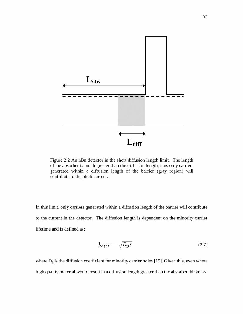
the absorber is far greater than the diffusion length (Fig. 2.2).
Page 54
33
Figure 2.2 An nBn detector in the short diffusion length limit. The length
of the absorber is much greater than the diffusion length, thus only carriers
generated within a diffusion length of the barrier (gray region) will
contribute to the photocurrent.
In this limit, only carriers generated within a diffusion length of the barrier will contribute
to the current in the detector. The diffusion length is dependent on the minority carrier
lifetime and is defined as:
𝐿𝑑𝑖𝑓𝑓 = √𝐷𝑝𝜏 (2.7)
where Dp is the diffusion coefficient for minority carrier holes [19]. Given this, even where
high quality material would result in a diffusion length greater than the absorber thickness,
Page 55
34
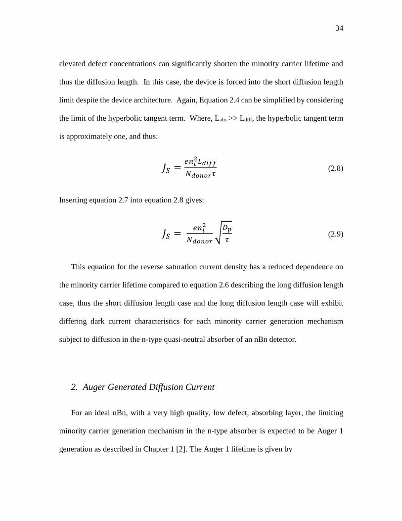
elevated defect concentrations can significantly shorten the minority carrier lifetime and
thus the diffusion length. In this case, the device is forced into the short diffusion length
limit despite the device architecture. Again, Equation 2.4 can be simplified by considering
the limit of the hyperbolic tangent term. Where, Labs >> Ldiff, the hyperbolic tangent term
is approximately one, and thus:
𝐽𝑆 =𝑒𝑛𝑖
2𝐿𝑑𝑖𝑓𝑓
𝑁𝑑𝑜𝑛𝑜𝑟𝜏 (2.8)
Inserting equation 2.7 into equation 2.8 gives:
𝐽𝑆 = 𝑒𝑛𝑖
2
𝑁𝑑𝑜𝑛𝑜𝑟√
𝐷𝑝
𝜏 (2.9)
This equation for the reverse saturation current density has a reduced dependence on
the minority carrier lifetime compared to equation 2.6 describing the long diffusion length
case, thus the short diffusion length case and the long diffusion length case will exhibit
differing dark current characteristics for each minority carrier generation mechanism
subject to diffusion in the n-type quasi-neutral absorber of an nBn detector.
2. Auger Generated Diffusion Current
For an ideal nBn, with a very high quality, low defect, absorbing layer, the limiting
minority carrier generation mechanism in the n-type absorber is expected to be Auger 1
generation as described in Chapter 1 [2]. The Auger 1 lifetime is given by
Page 56
35
𝜏𝐴1 =2𝑛𝑖
2𝜏𝐴1𝑖
𝑁𝑑𝑜𝑛𝑜𝑟2 (2.10)
where τiA1 is the Auger 1 lifetime for intrinsic material and is described by:
𝜏𝐴1𝑖 =
3.8×10⁻¹⁸𝜀𝑆2√1+𝜇(1+2𝜇)𝑒𝑥𝑝[(
1+2𝜇
1+𝜇)
𝐸𝑔
𝑘𝑇]
(𝑚𝑒∗ 𝑚𝑜⁄ )|𝐹1𝐹2|(𝑘𝑇 𝐸𝑔⁄ )
3/2 (2.11)
where εS is the relative static dielectric constant, me* is the electron effective mass, mo is
the mass of the electron, µ is the ratio of the conduction to heavy-hole band effective
masses, Eg is the bandgap energy, and F1 and F2 represent the overlap integrals from the
periodic portion of the electron wave function [46]. This expression for the Auger 1
lifetime is valid for III-V materials where the intrinsic carrier concentration is significantly
smaller than the donor density. The lifetime described by equation 2.10 may be applied to
equations 2.6 and 2.9 for the reverse saturation current density of the n-type absorber in
the long diffusion length and short diffusion length limits respectively.
2.1 Long Diffusion Length Limited Auger Current
It is expected that a typical, ideal, Auger-limited nBn will exhibit behavior in the long
diffusion length limit. In this case, combining equations 2.10 and 2.6 give the saturation
current density as:
𝐽𝑆𝐴1 =
𝑒𝐿𝑎𝑏𝑠𝑁𝑑𝑜𝑛𝑜𝑟
2𝜏𝐴1𝑖 (2.12)
Page 57
36
This equation suggests that for very low defect concentration nBn detectors with bulk
material absorbers dominated by the Auger 1 process, the only method by which Auger
currents may be suppressed is via limiting of the donor density. For this reason, Auger 1
generation is generally considered to be the fundamental limitation of nBn detector
performance. Even under moderately elevated defect concentrations, high donor density
nBn detectors will exhibit Auger 1-limited performance. It should be noted that
theoretically, strained-layer-superlattice based detectors will exhibit reduced Auger
generation, particularly for p-type absorbers, because the strain in the superlattice alters the
band structure in such a way that the overlap integrals between bands are reduced [47].
2.2 Short Diffusion Length Limited Auger Current
For very low defect concentrations the diffusion length is expected to be very long. In
this case, an nBn detector will only be in the short diffusion length limit and limited by
Auger 1 generation when the absorber thickness is very high. Generally, this would occur
when the substrate material matches the absorber material and no barriers exist near the
substrate/absorber interface. Where this is true, the Auger 1-limited, short diffusion length
limit suggests a saturation current density of:
𝐽𝑆𝐴1 = 𝑒𝑛𝑖√
𝐷𝑝
2𝜏𝐴1𝑖 (2.13)
according to equations 2.9 ad 2.10. In this case, Auger 1 cannot readily be suppressed by
adjusting donor doping, as the current density no longer depends on the donor density.
Page 58
37
3. Neutral Region Shockley-Read-Hall Generated Diffusion Current
For a defect limited nBn detector, the minority carrier lifetime is described by
Shockley’s theory of generation and recombination in semiconductors under the
assumption that TAT is not the dominant dark current mechanism [37, 38]. The original
SRH theory applies to both the depletion layer in a pn junction and the quasi-neutral
semiconductor region away from the junction. These neutral region SRH currents arise
from defect states in the bandgap of the neutral region. The minority carrier lifetime for
this generation mechanism can be described by:
𝜏𝑆𝑅𝐻 =1
𝑣𝜎𝑁𝑑𝑒𝑓𝑒𝑐𝑡 (2.14)
where v is the electron velocity, σ is the defect capture cross section, and Ndefect is the defect
density [19]. This lifetime is inversely proportional to the defect density, thus under
elevated defect concentrations the neutral region SRH lifetime will shorten and thus neutral
region SRH generation may limit device performance.
3.1 Long Diffusion Length Neutral Region SRH Current
If the limiting current mechanism is SRH generation in the neutral region, under
the long diffusion length limit, equation 2.6 and equation 2.14 result in a reverse saturation
current density for diffusion for the neutral region SRH mechanism as described by:
𝐽𝑆𝑆𝑅𝐻 =
𝑒𝑛𝑖2𝑣𝜎𝐿𝑎𝑏𝑠𝑁𝑑𝑒𝑓𝑒𝑐𝑡
𝑁𝑑𝑜𝑛𝑜𝑟 (2.15)
Page 59
38
Notably, the dark current density is directly proportional to the defect density, and the
thermal activation energy is equal to the full bandgap due to the temperature dependence
of the factor. This limit will apply for moderate defect densities where the minority
carrier lifetime is limited by neutral region SRH generation but the diffusion length is still
significantly longer than the absorber thickness.
3.2 Short Diffusion Length Neutral Region SRH Current
Under higher defect concentrations, the diffusion length may reduce to a value much
less than the absorber thickness. Here, the saturation diffusion current density is subject to
the long absorber, or short diffusion length, limit where Ldiff << Labs. In this limit, equation
2.9 can be combined with equation 2.14 giving the defect-limited saturation current density
in the short diffusion length limit as:
𝐽𝑆𝑆𝑅𝐻 =
𝑒𝑛𝑖2
𝑁𝑑𝑜𝑛𝑜𝑟√𝐷𝑝𝑣𝜎𝑁𝑑𝑒𝑓𝑒𝑐𝑡 (2.16)
Here, the saturation current density is proportional to the square root of the defect density
indicating a reduced dependence on defect concentration; however, for a typical nBn
architecture, operation in this limit suggests significant damage to the material, elevated
dark currents, and reduced quantum efficiency.
Even if the architecture of the nBn allows for long diffusion length limited performance
when material quality is very high, and thus the defect density is very low, moderate
elevation of the defect density may switch the detector into the short diffusion length limit
ni2
Page 60
39
and equation 2.16 will apply. In this case, neutral region SRH generation will dominate
the dark current over Auger 1 generation.
4. The Effect of Donor Concentration on Dark Current Characteristics
The donor density of the absorbing region can have a significant effect on the overall
dark current magnitude. Considering a typical nBn detector operating in the long diffusion
length limit, equations 2.12 and 2.15, for Auger 1 and SRH saturation current densities
respectively, have opposite dependences on the donor concentration. This implies that for
a given material defect density, there will be a doping that minimizes the dark current (Fig.
2.3).
Page 61
40
Figure 2.3 Modeled nBn saturation current density as a function of
increasing donor concentration for a detector natively in the long diffusion
length limit. Under low donor concentrations the dark current is dominated
by SRH generation, but under high donor concentrations the dark current is
dominated by Auger 1 generation. As the two processes have opposite
dependences on the donor concentration, there will be a doping
concentration which minimizes the saturation dark current density.
If the absorber doping is very low, it is likely that SRH generation will dominate the dark
current. As the absorber doping is increased, this SRH current will drop according to
equation 2.15. Even though the SRH current is decreasing while the donor density
Page 62
41
increases, the Auger current will be increasing. SRH will dominate the dark current until
the doping is such that the SRH generation current and the Auger 1 generation current
exhibit the same magnitude. This donor concentration will result in the lowest possible
dark current given the defect density. Further increases in the donor doping will only serve
to increase the dark current as Auger 1 generation will begin to dominate and Auger 1
current increases with donor concentration as described by equation 2.12. It is important
to notice that increasing the defect density increases the minimum dark current value, so to
maximize performance, the concentration of defects must be low enough to reach the
Auger 1 limit described by the doping of the detector absorber.
5. The Effect of Neutral Region SRH Generation on nBn Performance
Ideal nBn detectors would be expected to exhibit diffusion limited performance
originating from Auger 1 generation. Auger limited performance is associated with low
defect concentrations, long diffusion lengths, high quantum efficiency, and low dark
current [48]. These detectors should exhibit performance matching that suggested by Rule
07, a metric used to describe the performance of state-of-the-art MCT infrared detectors,
the best MWIR detectors currently available [23]. To date, however, barrier architecture
detectors have not exhibited performance matching Rule 07, yet still show diffusion limited
performance [49]. These diffusion currents originate from SRH, rather than Auger
generation processes. Furthermore, nBn detectors with defect concentrations elevated
beyond the native defect concentration, in contrast to conventional photodiodes, also
Page 63
42
maintain diffusion-limited performance under moderate biases; however, the dark current
density is elevated. For both of these cases, the diffusion current originates from a SRH
process in the quasi-neutral absorber rather than Auger 1 generation.
The best nBn detectors to date operate in the long diffusion length limit but as they
are limited by neutral region SRH generation, this likely indicates moderate defect
concentrations in the native, as-grown epitaxial material [12]. The predicted dark current
as a function of defect concentration for an nBn detector natively in the long diffusion
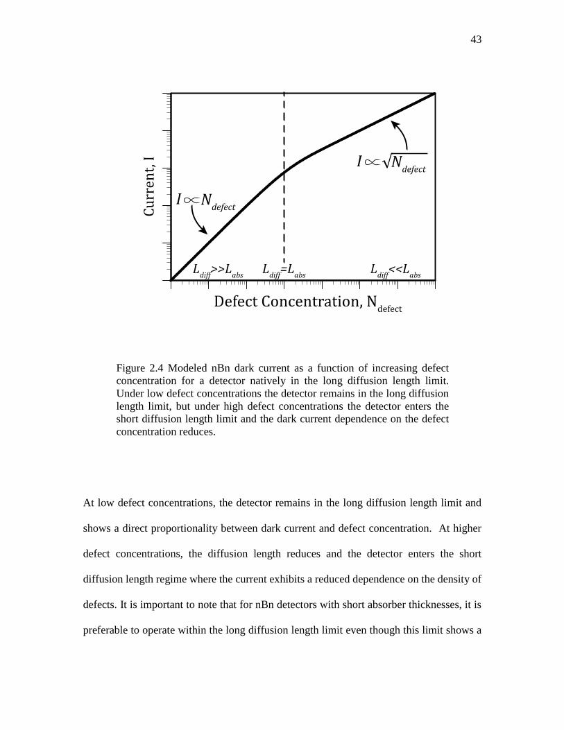
length limit is shown in Figure 2.4.
Page 64
43
Figure 2.4 Modeled nBn dark current as a function of increasing defect
concentration for a detector natively in the long diffusion length limit.
Under low defect concentrations the detector remains in the long diffusion
length limit, but under high defect concentrations the detector enters the
short diffusion length limit and the dark current dependence on the defect
concentration reduces.
At low defect concentrations, the detector remains in the long diffusion length limit and
shows a direct proportionality between dark current and defect concentration. At higher
defect concentrations, the diffusion length reduces and the detector enters the short
diffusion length regime where the current exhibits a reduced dependence on the density of
defects. It is important to note that for nBn detectors with short absorber thicknesses, it is
preferable to operate within the long diffusion length limit even though this limit shows a
Page 65
44
greater dependence on defect density compared to the short diffusion length limit. The
short diffusion length limit for these devices indicates significant damage to the epitaxial
structure resulting in a noticeable reduction in the quantum efficiency and increased noise.
6. Experimental Evidence of Neutral Region SRH Generation in nBn
Detectors
The effects of two types of defects in nBn detectors are reported here, representing
defects due to lattice mismatch and due to exposure to proton irradiation. A III-V
semiconductor based, type-II strained-layer superlattice, MWIR, nBn has been studied. It was
designed, grown, and processed by collaborators at Sandia National Laboratories. This nBn has a
Ga-free superlattice absorber with a 5.5µm, 50% cutoff wavelength at 120K and a typical nBn
device architecture. Following initial electrical characterization, the nBn was irradiated with
63MeV protons and current characteristics were measured at varying proton fluences. For the
duration of the irradiation study, the device was held at operating temperature and dark current
density-voltage (J-V) characteristics were taken after each high energy proton exposure. The effect
of proton irradiation is additive, thus each exposure and subsequent measurement represents the
effects of a higher total ionizing dose. Following proton irradiation, the device was returned to
room temperature and electrical characteristics were re-measured after approximately two weeks.
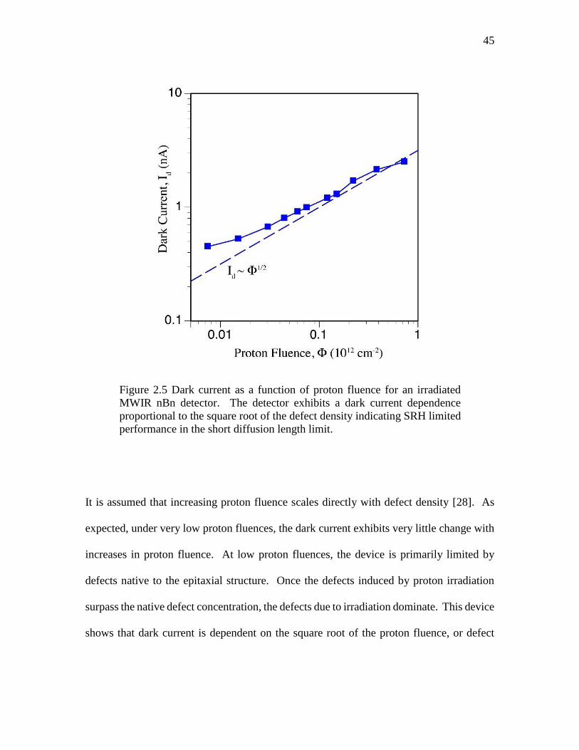
The dark current as a function of proton fluence is considered at a moderate bias of -300mV (Fig.
2.5).
Page 66
45
Figure 2.5 Dark current as a function of proton fluence for an irradiated
MWIR nBn detector. The detector exhibits a dark current dependence
proportional to the square root of the defect density indicating SRH limited
performance in the short diffusion length limit.
It is assumed that increasing proton fluence scales directly with defect density [28]. As
expected, under very low proton fluences, the dark current exhibits very little change with
increases in proton fluence. At low proton fluences, the device is primarily limited by
defects native to the epitaxial structure. Once the defects induced by proton irradiation
surpass the native defect concentration, the defects due to irradiation dominate. This device
shows that dark current is dependent on the square root of the proton fluence, or defect
Page 67
46
density, indicating this device is operating in the short diffusion length regime and is
limited by neutral-region SRH generation as Auger 1 generation does not depend on the
defect density nor the donor density to the one half power. This demonstrates that defects
are not resulting in an increase in donor concentration for nBn devices. As this device does
not show any defect concentration region where the dark current is directly proportional to
the defect density, this device had a high enough defect concentration to be in the short
diffusion length limit even before irradiation. Exposure to radiation only resulted in a
further reduction in the minority carrier lifetime and thus the diffusion length.
Detectors grown on mismatched substrates are subject to dislocation defects. The
defect concentration in the detector epitaxial structure depends on the thickness of the
buffer layer between the substrate and the absorbing region, decreasing inversely with
epitaxial layer thickness [50]. These effects were studied by examining InAs-based nBn
and conventional photodiode detectors grown on matched and mismatched substrates.
Temperature dependent J-V characteristics were measured and dark current density
Arrhenius analysis was performed for lattice matched and mismatched, nBn detectors (Fig.
2.6). The lattice mismatched nBn detector was grown on a GaAs substrate.
Page 68
47
Figure 2.6 Arrhenius analysis for dark current density of both lattice
matched and mismatched InAs nBn detectors. Both detectors exhibit
diffusion limited performance, as indicated by the slope of the lines that
indicated full bandgap thermal activation energies; however, the
mismatched substrate nBn shows dark currents elevated by an order of
magnitude.
Both the lattice matched and mismatched InAs nBn detectors show diffusion
limited performance with activation energies of 0.35eV, matching the bandgap of InAs,
but the lattice mismatched nBn exhibits dark currents elevated by approximately an order
of magnitude. The mismatched nBn has a significantly higher defect concentration and
thus has elevated dark currents in accordance with SRH generation in the quasi-neutral
region.
Page 69
48
6.1 Performance of SRH Limited nBns and Conventional Photodiodes
It is important to note that SRH generation in the quasi-neutral region is a significantly
smaller effect than SRH generation in a pn junction’s depletion region. Comparing the
performance of InAs nBn detectors to conventional InAs photodiodes demonstrates the
differing effects SRH generation has on each type of device. Photodiodes will be
dominated by depletion layer SRH while the nBn will only exhibit neutral region SRH and
will thus remain diffusion limited in the presence of elevated defect concentrations. The
practical result of this is a difference in dark current magnitude as well as a difference in
activation energies between the two devices (Fig. 2.7).
Figure 2.7 Arrhenius analysis for an InAs nBn detector (blue, ■) and a
conventional photodiode (red, ▲) grown on GaAs substrates. Even under
elevated defect concentrations the nBn exhibits reduced dark current
densities and full bandgap activation energies whereas the photodiode
exhibits a reduced activation energy.
Page 70
49
The mismatched InAs nBn, indicated by the blue line and square data points in figure 3,
remains diffusion limited and maintains an activation energy of 0.35eV or full bandgap
activation as described by the reverse saturation current density equations for neutral-
region SRH generation. The photodiode, shown in red with triangle data points, shows an
elevated current density and an activation energy of 0.11eV indicating a reduced thermal
activation energy in accordance with depletion region SRH and equation 1.7. Under
elevated defect levels, the nBn exhibits lower, but still elevated, defect densities and the
full bandgap activation energy allows for more efficient reduction in the dark current with
cooling compared to the defect limited photodiode.
6.2 RoA as it Relates to the nBn Detector
The reverse bias J-V characteristics for both the lattice matched and mismatched InAs
nBn and the irradiated MWIR nBn are shown in Figure 2.8.
Page 71
50
Figure 2.8 Reverse bias J-V characteristics for the lattice matched and
mismatched InAs (a) and the irradiated MWIR (b) nBn detectors. Both plots
show that increasing the defect concentration increases the current at reverse
biases greater than kT, but does not affect the reverse current at voltages
near zero.
Page 72
51
For both the case of defects induced via lattice mismatched growth and defects induced via
proton irradiation, there is a clear increase in reverse saturation current density as predicted
by the models for neutral region SRH generation and shown in figures 2.6 and 2.5
respectively. It is of particular importance to note the performance at very low reverse
biases, approximately less than -0.1mV bias, as neither induced defect resulted in a change
in the current characteristic around zero volts. This indicates that the defect-related
diffusion current, which dominates at larger reverse biases, is not the dominant current
mechanism at low reverse biases. Instead, low bias currents are apparently dominated by a
mechanism that is unrelated to defects. Due to this, there is not a significant change in the
zero-bias resistance with an increase in defect density for the nBn architecture; therefore,
the zero-bias resistance area product, RoA, is not a useful parameter to describe the
performance of the nBn. This is contrary to the common use of RoA as a figure of merit
for conventional photodiodes because there is a correlation between the value of RoA and
the shot noise in photodiodes as described in chapter 1.
Page 73
52
Chapter 3
Dark Current Filtering via Unipolar Barrier-Based Device
Architectures
Dark currents in MWIR photodetectors are generated via a variety of mechanisms
with each mechanism existing under a specific set of conditions and exhibiting a particular
set of behaviors. The limiting dark current mechanism for a particular detector is
determined by many factors including device architecture, detector material, detector size,
material defect density, applied bias voltage, operating temperature, and detector
environment. With such wide variation in dark current generation, finding robust,
adaptable epitaxial architectures capable of suppressing many noise generation
mechanisms can be a significant challenge but ultimately results in detectors with greatly
improved performance, compared to conventional architectures, even under less than ideal
conditions.
When designing an epitaxial structure for a detector, it is important to understand
not only how or why a particular dark current mechanism may dominate the electrical
performance, but where in the structure of the device the current is generated.
Understanding the spatial dependence of dark current generation can provide significant
insight into why a detector exhibits certain noise mechanisms and how best to engineer the
detector to minimize performance degradation due to elevated dark currents. Furthermore,
Page 74
53
if the highest possible performance is to be achieved, it is critical to understand what the
ultimate limiting dark current mechanism will be even if the device architecture
specifically inhibits one or more common dark current components. In a carefully
engineered and well corrected MWIR detector, fundamental material properties will be the
ultimate limit to device performance rather than material quality, device processing
considerations, or architecture specific dark current generation processes.
1. Spatial Makeup of Current Components in Photodetectors
It is understood that many current components comprise the overall dark current in a
given detector. The particular dark current components that may exist in a detector will be
determined by the detector architecture, the material defect density, and fundamental
materials properties. These dark current components in a bipolar device, such as a
photodiode, are carried by holes in some regions of the device and by electrons in the
others. The “spatial makeup” of the various current components, or the location(s) in the
device where the current changes from hole current to electron current, varies for each
current component. This location can be considered the location of current generation for
a given current mechanism, whether it is a desirable or undesirable current source.
Considering the spatial makeup of currents for a given device architecture can provide
insight into the factors limiting detector performance as well as methods for reducing noise
current generation in a device.
Page 75
54
1.1 Spatial Makeup of Current Components in the Simple Photoconductor
Considering the simple, n-type photoconductor, the primary desirable current
mechanism is that due to photo-generation of electron-hole pairs in the n-type absorbing
region. This region is also capable of thermally generating currents due to either Auger
processes, radiative generation, or defect-induced neutral-region SRH generation. (Fig.
3.1).
Figure 3.1. Spatial makeup of current mechanisms in the simple
photoconductor showing locations of carrier generation. Photocurrent and
thermally generated currents form in the n-type absorber while other
currents are generated at or near the electrical contacts.
Page 76
55
Other possible dark current mechanisms include surface leakage currents and majority
carrier flow from the anode to the cathode. Typically, majority carrier dark current is the
limiting dark current mechanism in simple photoconductors. In Figure 3.1, the surface
current is shown as electron current meaning the absorber material is assumed to have an
n-type surface conductivity as in the example of InAs. This is not always the case. The
surface conductivity may be p-type as in the case of InSb. For a p-type surface, the surface
leakage current is carried by holes. The case of an absorber with an n-type surface
conductivity is considered for the duration of this chapter.
1.2 Spatial Makeup of Current Components in the Conventional
Photodiode
The conventional photodiode prevents the flow of majority carrier dark current which
limits the photoconductor. These currents are blocked by the native, built-in barrier created
by the pn junction architecture. Like the photoconductor, some dark currents in a
photodiode may be generated in the quasi-neutral absorbing region with the same spatial
makeup as desirable photocurrent, but the pn junction also has a unique set of dark current
mechanisms, and thus noise generating processes (Fig. 3.2).
Page 77
56
Figure 3.2. Spatial makeup of currents in a conventional photodiode.
Currents can be generated in the n-type absorbing region, the junction
depletion region, or at the surface of the semiconductor.
Many dark current mechanisms, including TAT, B-B tunneling, and SRH generation
are junction related currents meaning that they occur in, near, or through the depletion
region of the device; surface currents can flow from any point along the surface profile of
the device. The majority of photocurrent is generated deep in the n-type absorbing region,
far from the space charge region and the p-type contact layer.
Page 78
57
2. Current Filtering via Unipolar Barriers
Unipolar barriers can be employed to filter out current components according to their
spatial makeups, dependent on the location of the barrier. In order for a current component
to flow, it must have a complete current path. This path requires either unimpeded majority
or minority carrier flow from contact to contact, or in the case of the generation of electron-
hole pairs within the semiconductor bulk material, a free path to the respective contacts for
both electrons and holes before electron-hole pair recombination. Blocking the anode to
cathode path for either electrons or holes or blocking either the hole current path or electron
current path for currents generated via electron-hole pair excitation will essentially cut off
those current mechanisms, as a complete current path no longer exists. Unipolar barriers
are an ideal candidate for selectively filtering out unwanted currents while allowing a
complete current path for desirable currents simply because the location of the barrier can
be adjusted within a device architecture and because it only blocks one carrier type, either
electrons or holes.
The analysis here is restricted to electron blocking unipolar barriers; however, the same
principles will apply for hole blocking barriers as well. In either case, barriers may be
either minority or majority carrier unipolar barriers depending on the conductivity of the
material in which the barrier is placed, either p-type or n-type.
Page 79
58
2.1 Current Filtering in the nBn Detector
To illustrate these concepts, consider first the nBn detector. The nBn detector is
subject to all of the same current generation processes as the simple photoconductor
since it is based on this architecture. For this reason, the spatial makeup of current
components in the nBn and photoconductor, as shown in Figure 3.1, are the same.
There are two locations in which the barrier may be placed in the simple
photoconductor. The first is near the cathode (Fig. 3.3).
Figure 3.3. Properly locating the unipolar barrier in an nBn is critical to
maximizing device performance. Locating the barrier close to the bottom
contact will block dark currents, but will also severely limit the photocurrent
making this a poor location for a unipolar barrier.
Page 80
59
With this barrier location, all electron flow is essentially blocked so no dark current
mechanism has a complete current path; however, this is not a useful place for the barrier
in an nBn because the unipolar barrier will block electron flow from the photocurrent thus
suppressing this desirable current mechanism as well.
A far better placement of the unipolar barrier in an nBn is very near the cathode as
shown in Figure 3.4.
Figure 3.4. The ideal barrier placement for an nBn is near the top contact.
Currents generated at the surface/contact interface are blocked by the
barrier, but photocurrent is not limited. Thermally generated diffusion
currents in the absorbing layer cannot be blocked because they share the
same spatial makeup as the photocurrent.
Page 81
60
In this case, there is still a free path for hole flow to the cathode from photo-generated
carriers, but also from diffusion of holes generated via thermally related processes in the
n-type quasi-neutral absorber. Here, diffusion-related dark currents share the same spatial
makeup as the photocurrent and cannot be suppressed by a unipolar barrier; however,
electrons from majority carrier dark current and surface current are blocked by the electron
blocking unipolar barrier, so these dark current mechanisms are essentially filtered out by
the unipolar barrier. This dark current filtering is the primary reason the nBn architecture
shows significant improvements over both the simple photoconductor and the conventional
photodiode.
3. The Unipolar Barrier Photodiode
The advantages the unipolar barrier brought to the simple photoconductor in the nBn
can also be extended to the conventional, pn junction-based photodiode architecture. In
this way, the advantages afforded by a pn junction, a built-in electric field and photovoltaic
detection can be extended to the family of unipolar barrier architecture detectors [17].
The unipolar barrier photodiode is based on a conventional photodiode with a
unipolar barrier inserted into the pn junction structure. Consider photodiodes where the
optical absorption occurs in the n-type region. Photo-generated holes travel from the n-
region across the junction to the p-region contact, while photo-generated electrons flow in
the n-type region of the detector from the point of generation to the n-side contact. Recall
that any dark current component that shares this same spatial makeup as the photocurrent
Page 82
61
cannot be eliminated by a unipolar barrier without also filtering out the photocurrent;
however, dark current components with different spatial makeups can be eliminated by a
properly located unipolar barrier. It is instructive to consider placing the barrier in several
locations within the conventional photodiode architecture. Figure 3.5 shows a placement
of the unipolar barrier such that virtually all dark current mechanisms are blocked.
Figure 3.5. As with the nBn architecture, locating the unipolar barrier in a
UBP near the bottom contact will limit all currents including the
photocurrent, thus this is a poor location for a unipolar barrier in the UBP
architecture.
Page 83
62
Similarly to the nBn, this is not a useful placement for the barrier in the photodiode
architecture, the barrier successfully blocks diffusion currents, junction related currents,
and surface currents; however, the diffusion dark current generated in the n-type absorber
shares the same spatial makeup as the desirable photocurrent. This significantly limits the
amount of photocurrent that can be collected by the device making this a poor architecture
for a UBP.
3.1 p-Region Unipolar Barrier Photodiode
The unipolar barrier can be placed in the p-type region of a conventional photodiode
architecture. This is called a p-side UBP or a pUBP (Fig. 3.6).
Figure 3.6. Bulk band diagram of a p-side UBP. Photocurrent is generated
deep in the n-type region, thus photocurrent is not blocked by the unipolar
barrier, but dark currents generated above the barrier will be blocked.
Page 84
63
This device architecture already has a significant advantage over the conventional
photodiode as currents generated near the cathode of the device, typically surface leakage
current, will naturally be suppressed while photocurrent generated deep in the n-type
absorber flows unimpeded.
3.1.1 Current Filtering in the p-Region Unipolar Barrier Photodiode
As the UBP is based on the conventional photodiode, it is subject to the same dark
current mechanisms and spatial makeup as the conventional photodiode as described above
and shown in Figure 3.2. Taking into account the placement of the unipolar barrier in the
pUBP, the filtering via spatial makeup property of the unipolar barrier as it relates to this
architecture can readily be shown (Fig. 3.7)
Page 85
64
Figure 3.7. Locating the unipolar barrier in the p-region of a UBP
successfully blocks the flow of surface currents, but junction related
currents will still flow as these currents, along with the photocurrent and
thermally generated diffusion currents, are formed below the barrier in the
epitaxial structure.
For the pUBP, the only dark current mechanism typically generated above the unipolar
barrier is surface leakage current, thus the pUBP will exhibit no surface currents; however,
the junction related dark currents, TAT, SRH, and B-B tunneling are not blocked by the
barrier and will flow unimpeded if they are generated (Fig. 3.8).
Unipolar
Barrier
Page 86
65
Figure 3.8. Bulk band diagram of a pUBP showing photo-generation and
junction related dark currents. The location of the unipolar barrier in a
pUBP does not block the flow of either holes or electrons for junction
related SRH or tunneling currents.
Because SRH and TAT currents are related to trap states due to defects, pUBP detectors
are not a particularly useful architecture when the defect density of a detector is likely to
be elevated or for very small bandgap materials where direct B-B tunneling is a significant
concern under typical operating conditions [37, 40, 51].
3.2 n-Region Unipolar Barrier Photodiode
The unipolar barrier can also be placed in the n-type region of a conventional
photodiode architecture, preferably near the edge of the depletion region. This is called an
n-side UBP or an nUBP (Fig. 3.9).
Page 87
66
Figure 3.9. Bulk band diagram of an n-side UBP. Photocurrent is generated
deep in the n-type region, thus photocurrent is not blocked by the unipolar
barrier, but dark currents generated above the barrier will be blocked.
This device architecture, like the pUBP is also capable of blocking surface leakage currents
but now, the barrier will block the flow of electrons generated in the depletion region of
the detector. Keeping the barrier as close to the depletion layer as possible will guarantee
that photocurrent generated deep in the n-type absorber flows unimpeded.
3.2.1 Current Filtering in the n-Region Unipolar Barrier Photodiode
The nUBP architecture represents the placement of the unipolar barrier in a UBP which
exhibits the maximum potential for current filtering via unipolar barriers in pn junction
based detectors (Fig. 3.10).
Page 88
67
Figure 3.10. Locating the unipolar barrier in the n-type absorbing region in
a UBP on the edge of the depletion region of the pn junction will
successfully block both surface currents and depletion region generated
dark currents; however, thermally generated diffusion currents sharing the
same spatial makeup as the photocurrent are not blocked by the barrier.
Keeping the barrier layer close to the junction interface limits the amount of
photocurrent that is blocked by the barrier.
When the electron blocking unipolar barrier is placed just downstream of electrons
generated in the depletion layer, the current path for these depletion layer electrons is
effectively cut off (Fig. 3.11).
Page 89
68
Figure 3.11. Bulk band diagram of an nUBP showing photo-generation and
junction related dark currents. The location of the unipolar barrier in an
nUBP effectively blocks the flow of electrons for junction related SRH and
tunneling currents.
As surface leakage currents are generated above the space charge region or along the
surface of the junction down to the barrier layer, the flow of surface electrons is also
blocked. Like the pUBP, thermally generated diffusion currents due to neutral region SRH
generation, Auger processes, and radiative processes that share the same spatial makeup as
the photocurrent cannot be filtered out by the unipolar barrier without also suppressing
photocurrent generation as well.
4. Advantages and Limitations of Unipolar Barrier Architectures
Unipolar barrier architectures show significant advantages over conventional
photodetector architectures, but unipolar barriers do create significant materials limitations
and cannot effectively block all dark current mechanisms. It is important to keep this under
Page 90
69
consideration when designing a device structure for a particular application. Keeping in
mind both the advantages and limitations unipolar barriers afford and impose will result in
the best possible detector design.
4.1 Advantages of Unipolar Barrier-Based Epitaxial Architectures
Infrared detectors utilizing unipolar barriers show several advantages over
conventional devices. First, unipolar barriers can be employed to remove the effects of
surface leakage currents resulting in a device, without requiring surface passivation. This
alone can significantly save on time and cost of manufacturing devices. Furthermore, in
materials for which there is no known effective surface passivant, unipolar barriers
eliminate this limitation. When properly employed, unipolar barriers can also block
junction related currents in photodiodes including those due to direct B-B tunneling, SRH
generation, and TAT. Both SRH and TAT currents are related to defects in the material,
thus the UBP is a more defect tolerant design scheme than the conventional photodiode.
Even in cases where defects are unavoidable, or where creating sufficiently defect-free
material is a considerable challenge, unipolar barriers can allow for greatly improved
performance over a large temperature range when compared to conventional architectures.
Unipolar barrier-based device architectures are not limited to those described here.
Unipolar barriers can be engineered as electron barriers or hole barriers and as minority or
majority carrier barriers. It is possible to have a barrier with a large conduction band offset
or a large valence band offset thus allowing for a wider range of materials to consider as a
Page 91
70
barrier material. A hole barrier analog to the nBn, a pBp, should operate in an analogous
manner to the nBn with the same advantages. The pBp should be used in cases where the
surface of the absorbing material exhibits p-type conductivity. Similar considerations
apply to the barrier in the UBP.
Overall, this analysis suggests that unipolar barrier devices should operate with
improved performance when compared to conventional devices. The nBn has already
shown significant reductions in dark current, which directly translates into a reduction in
the noise of the device. Often, they also have the ability to operate at a higher temperature
with similar performance to conventional devices and/or operate with improved
performance at lower temperatures [11, 44]. Experimentally obtained dark current
characteristics of UBPs will be described in the next chapter.
4.2 Limitations of Unipolar Barrier-Based Epitaxial Architectures
Unipolar barrier devices are often limited by materials considerations. A perfect barrier
material, like AlAs0.18Sb0.82 in InAs, does not exist in every materials system. Many
material systems would require the growth of a graded barrier in which a doped, minority
carrier barrier is grown by grading between the material surrounding the barrier and a
material with a larger bandgap. The doping and grading result in either the valence band
or conduction band being pinned to the level of the surrounding material depending on
whether it is an electron or hole blocking barrier. A graded barrier can only be a minority
Page 92
71
carrier barrier thus a UBP with a graded barrier cannot block junction related currents like
SRH, direct B-B tunneling, and TAT currents (Fig. 1.12).
Figure 3.12. Band diagram for a graded barrier pUBP. The graded barrier
must be a minority carrier barrier, thus it cannot be employed to block
currents that manifest in the depletion layer of the device.
In this way, graded barrier UBP devices are not any more defect tolerant than the
conventional photodiode since they cannot block defect related currents arising through
defect states in or near the depletion layer.
It is important to locate the barrier in a region of the device where the photocurrent
will not be impeded or limited. As a result of this, it is not possible to filter out diffusion
current using a unipolar barrier. The carriers that primarily contribute to diffusion current
are generated in the absorbing region where the photocurrent is generated, thus the
photocurrent and the diffusion current share the same spatial makeup and one cannot be
removed without also filtering out the other. For this reason, unipolar architecture devices
cannot significantly limit diffusion currents arising from neutral region SRH or Auger
generation.
Page 93
72
Chapter 4
Dark Current Characteristics of Unipolar Barrier
Photodiodes
From a fundamental standpoint, the unipolar barrier photodiode has several
advantages over the conventional photodiode while maintaining the benefits of the pn
junction-based architecture. Although the nBn and UBP share the same general current
filtering ability afforded by the unipolar barrier, the electrical characteristics of the UBP
differ from that of the nBn in several ways. The UBP exhibits a photovoltaic nature, carrier
drift via the built-in electric field of the pn junction, and diode rectification in the I-V
characteristic. Within the UBP architecture itself, barrier placement has a dramatic effect
on device performance. The limiting dark current mechanism for the UBP will change
depending on material quality and barrier location within the epitaxial structure.
To demonstrate the effect of barrier placement on device performance, UBPs with
barriers in the n-type absorbing region or the p-type contact region have been fabricated
alongside comparable conventional photodiodes. The photodiodes are demonstrated with
InAs absorbing regions and electron blocking, AlAs0.18Sb0.82 unipolar barriers. In UBPs,
whether the unipolar barrier acts as a majority or minority carrier barrier depends on the
material conductivity into which the barrier is placed. AlAs0.18Sb0.82 is a near perfect match
as a unipolar barrier for InAs in that it has a significantly larger bandgap than InAs, is
Page 94
73
nearly lattice matched to InAs while maintaining a zero valence band offset, and has well
understood growth conditions [52, 53]. This is the same materials system in which the nBn
was initially demonstrated thus InAs UBPs serve as a direct analog to the first nBn.
1. Unipolar Barrier Photodiode Design, Growth, and Processing
In order to study the current filtering characteristics of UBPs, both nUBP and pUBP
were grown and processed into variable area detectors alongside matching conventional
photodiodes. This allows for direct comparison of dark current characteristics between the
three architectures with the conventional photodiode serving as the control in the
experiment. Although conventional pn junction growth is common, and nBn growth has
previously been demonstrated, UBP growth was not performed previous to this study.
1.1 InAs-Based Unipolar Barrier Photodiodes
InAs was chosen as the absorbing material because of the existence of the AlAs0.18Sb0.82
unipolar barrier, the use of InAs as the demonstration material for the original nBn detector,
and the surface Fermi level pinning of InAs [32]. Since the surface Fermi level in InAs is
pinned in the conduction band, a shunt path for electron flow exists across the surface. Due
to this effect, if a conventional pn junction is grown in InAs, even though the bulk material
will contain a pn junction, the surface of the device will resemble a highly conductive,
degenerate n-type material (Fig. 4.1).
Page 95
74
Figure 4.1. Bulk band diagram (top) of an InAs pn junction and how it
compares to the surface band diagram (bottom) for the same InAs pn
junction. The surface Fermi level pinning in InAs leads to a highly
conductive n-type surface.
This highly conductive, n-type shunt path for electrons at the surface of InAs should
result in a significant amount of surface leakage current. It is expected that conventional
photodiodes grown in InAs will be limited by surface leakage current.
By comparison, both nUBP and pUBP are capable of blocking the flow of this
surface current because of the current filtering nature of the electron blocking unipolar
barrier when it is applied to an InAs pn junction (Fig. 4.2).
Page 96
75
Figure 4.2. Bulk band diagram (top) of an InAs pUBP and how it compares
to the surface band diagram (bottom) for the same InAs pUBP. The flow of
surface electrons is blocked by the unipolar barrier.
It is expected that nUBP and pUBP will not exhibit surface leakage limited performance
because the unipolar barrier blocks surface electrons from flowing.
The difference in performance between nUBP and pUBP is expected to be related
to depletion layer generated dark currents. The pUBP, will not exhibit surface leakage
current, but will exhibit junction-related dark current mechanisms like depletion layer
Page 97
76
SRH, TAT, and direct B-B tunneling. The nUBP is expected to remain completely
diffusion limited although the limiting dark current mechanism may be Auger 1 generation
or defect-induced neutral-region SRH generation.
1.2 Molecular Beam Epitaxy Growth of Unipolar Barrier
Photodiodes
All three diode architectures were grown by solid source MBE on a Riber 32P system
utilizing As2 and Sb4. The conventional photodiodes were grown on unintentionally doped,
n-type InAs substrates. A 2μm, unintentionally doped n-type InAs layer with a carrier
concentration of n≈1016cm-3 was deposited followed by 2,000Å of beryllium doped p-type
InAs with a carrier concentration of p≈1018cm-3. The growth was completed with a 1,000Å
p+-type InAs contact layer in which the doping level was graded from p≈1018cm-3 to a
maximum doping concentration of p≈1019cm-3 (Table 4.1).
Table 4.1. Epitaxial structure and growth conditions of a control, InAs pn
junction. This structure is a conventional photodiode.
Layer Material Thickness Growth Temperature Growth Rate
n-type InAs:ud 2 µm 420 °C 1.0 ML/s
p-type InAs:Be 2,000 Å 420 °C 1.0 ML/s
p+
-type contact InAs:Be 1,000 Å 420 °C 1.0 ML/s
Page 98
77
The conventional photodiode is grown without growth stops, at a single temperature of
420°C, a known transition temperature and typical growth temperature for InAs.
The growth characteristics for the pUBP were identical to the conventional
photodiode up to the location of the ternary unipolar barrier at which point an added growth
stop to increase the substrate temperature was added. AlAs0.18Sb0.82 prefers a higher
growth temperature than InAs, so the temperature of the substrate was increased by
approximately 45°C during a two minute growth stop under constant As2 flux before the
1,000Å barrier layer was grown. The growth conditions and epitaxial structure of the
pUBP is given in Table 4.2.
Table 4.2. Epitaxial structure and growth conditions of a p-side, InAs-based
unipolar barrier photodiode.
The barrier was doped with the same beryllium flux as the InAs p-type material. A five
minute growth stop followed under both As2 and Sb4 fluxes while the temperature was
returned to the InAs growth temperature.
Layer Material Thickness Growth Temperature Growth Rate
n-type InAs:ud 2 µm 420 °C 1.0 ML/s
p-type InAs:Be 1,000Å 420 °C 1.0 ML/s
Barrier AlAs 0.18 Sb 0.82 :Be 1,000 Å 465 °C 1.0 ML/s
p-type InAs:Be 1,000 Å 420 °C 1.0 ML/s
p+
-type contact InAs:Be 1,000 Å 420 °C 1.0 ML/s
Page 99
78
To complete the device, 1,000Å of additional Beryllium doped p-type InAs was
deposited followed by the same graded, 1,000Å p+-type InAs contact layer present in the
conventional photodiode.
The nUBP contained the same growth stop as the pUBP; however, it occurred after
1µm of unintentionally doped n-type absorbing region growth (Table 4.3).
Table 4.3. Epitaxial structure and growth conditions of an n-side, InAs-
based unipolar barrier photodiode.
In the case of the nUBP, the unipolar barrier layer is grown unintentionally doped. After
the growth stop, an additional 1µm of undoped InAs absorbing region growth occurred.
The p-type region and p+-type contact layer were grown identically to that of the
conventional photodiode.
For all device growths, substrate temperatures were measured with a pyrometer and
growth rates were calibrated using reflection high-energy electron diffraction (RHEED)
oscillations performed during a separate growth.
Layer Material Thickness Growth Temperature Growth Rate
n-type InAs:ud 1 µm 420 °C 1.0 ML/s
Barrier AlAs 0.18 Sb 0.82 :ud 1,000 Å 465 °C 1.0 ML/s
n-type InAs:ud 1 µm 420 °C 1.0 ML/s
p-type InAs:Be 2,000 Å 420 °C 1.0 ML/s
p+
-type contact InAs:Be 1,000 Å 420 °C 1.0 ML/s
Page 100
79
1.3 Photolithographic Processing
All devices were processed identically utilizing standard III-V photolithographic
techniques, metal deposition, and wet chemical etching for mesa definition. Each device
architecture was etched down beyond the epitaxially grown material to the InAs substrate
where the bottom contact was located. This choice was made because it provides the most
direct comparison between the unipolar barrier-based diode architectures and the
conventional photodiode. Typically, unipolar barrier architecture detectors are designed
so that they can be etched to the unipolar barrier layer and no further. This assures that no
absorber surface is exposed below the barrier where surface currents can be generated.
Because the pUBP and nUBP were etched past the epitaxially defined barriers, it is possible
for surface conduction to occur in the devices as processed, although at a significantly
reduced magnitude compared to conventional architectures.
2. Room Temperature J-V characteristics of UBPs
Measurements of current density, J, as a function of voltage were taken at room
temperature for both nUBP and pUBP devices. Detector areas ranged from 1.4x10⁻⁵ cm2 to
1.6x10⁻³ cm2. Figure 4.3 shows J-V characteristics for both types of devices.
Page 101
80
Figure 4.3. J-V characteristics for a unipolar barrier photodiode with the
barrier in the p-type region (top) and with the barrier in the n-type region
(bottom). Increasing current with reverse bias in the p-type region devices
indicates the presence of tunneling currents or SRH generation. Nearly
voltage independent current with reverse bias in the n-type region devices
indicates suppression of tunneling currents and diffusion limited
performance.
Page 102
81
J-V characteristics for pUBP show a clear increase in the current density with reverse
bias. This behavior is typical of depletion region generated tunneling and SRH currents.
Devices that exhibit a nearly voltage independent current density characteristic at relatively
low reverse bias and the onset of increasing current density at higher reverse bias display
the characteristics of TAT tunneling which requires a reverse bias before it begins to
dominate at room temperature. Devices which show an increasing current density from
zero bias into reverse bias exhibit SRH limited performance. SRH does not require a
reverse bias in order to be generated [54].
As expected, nUBP detectors exhibit improved reverse bias characteristics because of
the suppression of junction related currents. These devices show a reverse bias current
density characteristic that is nearly voltage independent indicating that only diffusion
current is present and tunneling has been completely removed. It is difficult to tell what
the limiting diffusion current mechanism is for these devices without a more complete
analysis; however, it should be noted that the reverse saturation current density of two
nUBPs represented in Figure 4.3 are elevated beyond the remaining devices yet still show
diffusion limited performance. Assuming that only Auger 1 or neutral region SRH are
likely to limit these devices, it is very likely that these two detectors are showing
performance limited by neutral region SRH as the Auger 1 current should be the same for
every device on a single wafer. It is likely that nUBP devices with these SRH elevated
saturation current densities are on a portion of the semiconductor wafer where the native
grown in defect density is higher than the surrounding material.
Page 103
82
An interesting parallel can be drawn for FPA performance. FPAs will have many
devices over a large growth area. The defect concentration may change across the epitaxial
surface due growth related factors. This variation in defect density will affect the
performance of each individual pixel in the array, thus it is advantageous to choose a
detector architecture which is as defect tolerant as possible. If the elevated neutral-region
SRH nUBP devices were grown as conventional photodiodes, those two devices would be
severely limited by depletion region SRH, but since they are grown with a unipolar barrier
in the n-type layer, that higher magnitude, defect-related, depletion region SRH is
suppressed and the device remains diffusion limited albeit with an increased reverse
saturation current density compared to surrounding detectors.
2.1 Representative Reverse Bias J-V Characteristics of Room
Temperature nUBP and pUBP Detectors
Representative reverse bias J-V characteristics were chosen for room temperature
nUBP and pUBP detectors showing diffusion limited performance, depletion region SRH
limited performance, and TAT limited performance. These J-V characteristics were fit to
the standard equations for the limiting mechanism of each detector, either diffusion current,
depletion region SRH, or TAT. The current density due to diffusion processes in the n-
type quasi-neutral absorber is given by:
𝐽𝑑𝑖𝑓𝑓 =𝑒𝑛𝑖
2(𝑇)
𝑁𝑑√
𝐷𝑝
𝜏𝑜(𝑒𝑒𝑉 𝑘𝑇⁄ − 1) (4.1)
Page 104
83
where e is the charge of the electron, ni(T) is the intrinsic carrier concentration, Nd is the
donor density, Dp is the minority carrier diffusion coefficient, τo is the diffusion lifetime,
V is the applied voltage, k is the Boltzmann constant, and T is the temperature [54]. The
current density due to the depletion region SRH generation process is given by:
𝐽𝑑−𝑆𝑅𝐻 =𝑒𝑛𝑖(𝑇)𝐿𝑑𝑒𝑝(𝑉)
2𝜏𝑜
2𝑘𝑇
𝑒(𝑉𝑏𝑖 − 𝑉)𝑠𝑖𝑛ℎ (−
𝑒𝑉
2𝑘𝑇) ∫
𝑑𝑢
𝑢2 + 2𝑢𝑒−𝑒𝑉 2𝑘𝑇⁄ + 1
∞
0
(4.1)
as previously described in chapter 1 (Equation 1.7), and the current density due to TAT is
given by:
𝐽𝑇𝐴𝑇 =𝑒2𝑚𝑇𝑉𝑀2𝑁𝑇
8𝜋ħ3 𝑒𝑥𝑝 (−4√2𝑚𝑇(𝐸𝑔−𝐸𝑡)
3
3𝑒ħ𝐹(𝑉)) (4.2)
where mT is the tunneling effective mass, M2 is a matrix element related to the trap potential
and is assumed to have a constant value, NT is the trap density, ħ is Planck’s constant
divided by 2π, Eg is the material bandgap, Et is the trap energy with respect to the valence
band edge, and F(V) is the electric field [37, 38, 40, 54]. Surface leakage current is left out
of the model as it is expected to be suppressed in UBP detectors. Fit parameters for the
models in question include diffusion lifetime, SRH lifetime, and trap or defect density.
Results of the fit are shown in Figure 4.4.
Page 105
84
Figure 4.4. 300K current density-voltage measurements of unipolar barrier
photodiodes (solid lines), and modeled expressions (dotted lines: light blue
is TAT, dark blue is SRH, and red is diffusion current). pUBPs typically
exhibit either TAT-limited behavior or SRH-limited behavior, examples of
which are shown in light blue and dark blue, respectively. nUBP diodes
exhibit diffusion-current-limited performance, shown in red.
Best fits for all devices indicate diffusion current on the order of ≈0.1-0.2A/cm2 for reverse
voltages much larger than kT, while devices showing significant SRH or TAT are well fit
by trap or defect densities of ≈1013-1014cm-3. SRH dominated devices typically fit to SRH
lifetimes in the range of ≈1-10ns, while devices dominated by other mechanisms show
≈50ns SRH lifetimes. It is clear that both types of unipolar barrier photodiodes block the
flow of surface leakage currents; however, the models prove that pUBP detectors are
dominated by either tunneling currents or SRH generation in the depletion region. nUBP
all exhibit diffusion limited performance indicative of the suppression of junction related
currents. Diffusion current cannot be eliminated by a unipolar barrier as it shares the same
spatial makeup as the photocurrent.
Page 106
85
3. Arrhenius Analysis of p-Region Unipolar Barrier Photodiode
The temperature dependence of the J-V characteristics can give insight into the limiting
current mechanism. As has been shown, diffusion currents maintain full bandgap
activation energies as the temperature of a detector is decreased. SRH currents generated
in the depletion region of pn junction based devices exhibit half bandgap activation
energies when depletion layer SRH is limiting. Tunneling and surface leakage currents are
expected to be relatively temperature independent.
I-V characteristics were experimentally obtained over a temperature range of 100K
to 300K for both a conventional InAs photodiode and pUBP with equal areas of
1.83x10⁻⁴cm2. Representative high and low temperature I-V characteristics are shown for
each detector in Figure 4.5.
Page 107
86
Figure 4.5. Representative I-V characteristics of a conventional InAs
photodiode (top) and InAs unipolar barrier photodiode (bottom) at both a
high and low temperature.
Page 108
87
At T(K)=220K, both devices exhibit a region where the current is approximately voltage
independent, indicating that diffusion current is the dominant dark current mechanism.
Current density, defined as a measured current divided by a mesa area, was extracted from
the I-V characteristics at a nominal reverse bias voltage of 100mV and plotted as a function
of 1000/T[K] (Fig. 4.6).
Figure 4.6. Dark current density as a function of reciprocal temperature for
a conventional photodiode and a pUBP. Notice the improved performance
of unipolar barrier photodiode below 150K.
The presence of temperature independent surface current is clearly observable at lower
temperatures in the conventionalphotodiode but is absent in the pUBP down to the noise
limits of the measurement equipment. The conventional photodiode is diffusion current
limited above 150K where the thermal activation energy is approximately equal to the
Page 109
88
bandgap of InAs as measured by the slope of the temperature dependent portion of Figure
4.6. This behavior is in agreement with the I-V characteristic in Figure 4.5. Temperature
independent surface currents become dominant below 150K.
The unipolar barrier device remains diffusion current limited down to at least 130K.
This demonstrates that the dark current limit in the unipolar barrier photodiode is at least
20 times lower than the dark current limit in a comparable conventional photodiode. Dark
currents are related to noise through the standard shot noise model as described in Chapter
1 [55]. A reduction on the dark current by a factor of 20 corresponds to a decrease in noise
currents by a factor of the square root of 20.
4. RoA of an n-Side Unipolar Barrier Photodiode
The zero bias resistance-area product, RoA, was described as a useful figure of merit
for photodiodes in Chapter 1. It is a good parameter because there is an inverse relationship
between the value of RoA and the noise generating dark current in photodiodes. A high
RoA value indicates good performance while a low RoA value indicates that performance
is being significantly limited by a dark current mechanism.
J-V characteristics were taken over a temperature range of 60K to 300K for a
conventional, InAs photodiode and an nUBP with matching areas of 4.41x10⁻⁴ cm-2. RoA
values were extracted from the J-V characteristics and plotted as a function of reciprocal
Page 110
89
temperature. Also plotted with this data is the Rule 07 line as described in Chapter 1 for a
diffusion limited detector (Figure 4.7) [23].
Figure 4.7. RoA of a conventional photodiode and comparable nUBP
detector. The unipolar barrier photodiode show improvements in RoA of
over six orders of magnitude and performance close to the Rule 07 line
indicating near Auger limited performance.
The conventional photodiode becomes surface leakage current limited at a temperature
of 225K as indicated by the nearly temperature independent RoA at all lower temperatures.
This significantly limits the ultimate RoA value for a conventional photodiode, in this case,
to a value of 8.95 Ω-cm2. Surface leakage current and junction related dark currents are
significantly reduced in the nUBP which ultimately achieves an RoA value of 1.12x10⁷ Ω-
cm2 indicating over 6 orders of magnitude improvement when compared to the
conventional device. At higher temperatures, both devices show diffusion limited device
performance. The slope of each curve in this region indicates an activation energy roughly
Page 111
90
equal to the bandgap of InAs. It is important to note that the nUBP shows performance in
close proximity to the Rule 07 line indicating near Auger 1 limited performance. As the
device does not match or surpass the Rule 07 line, it is likely that the detector is limited by
neutral region SRH generation even though this device shows nearly the best performance
with respect to Rule 07 of any III-V based, unipolar barrier architecture detector available
in the published literature to date [12, 49].
5. Summary of UBP Dark Current Performance
These observations regarding the dark currents of InAs based conventional photodiodes
and pUBP and nUBP detectors match the expectations outlined in Chapter 3. Upon
cooling, conventional photodiodes quickly become limited by surface leakage currents.
The addition of the unipolar barrier to the p-type layer in the pUBP successfully suppressed
surface leakage currents resulting in improved performance; however, room temperature
I-V characteristics show that pUBP detectors may be limited by defect induced, depletion
region dark currents. When the unipolar barrier is moved into the n-type region of the
photodiode, even these junction related dark currents are suppressed showing over six
orders of magnitude in improvements over the performance of a conventional photodiode.
Furthermore, like the nBn detector, the nUBP remains diffusion limited even in the
presence of elevated defects. This data suggests that the current filtering properties of
unipolar barriers as proposed in Chapter 3 are real effects, thus taking into account the
spatial makeup of current components and utilizing unipolar barriers when appropriate and
Page 112
91
possible is a robust and intelligent strategy when designing device architectures to improve
infrared detector performance.
Page 113
92
Chapter 5
Summary and Conclusions
Compound semiconductor device performance will continue to improve, as it has
for decades, but not without improvements in material quality, a deeper understanding of
limiting current mechanisms, and careful and innovative epitaxial design. To that end, the
efforts presented here provide greater insight into the dominating dark current mechanisms
in high performance MWIR detectors, demonstrate strategies for improving design of
epitaxial structures, and describes a novel device architecture, the unipolar barrier
photodiode. These concepts have the potential to reach beyond that which has been
described here.
It is possible to extend the unipolar barrier concept to other, shorter wavelength
bands for light detection, and perhaps more significantly, potentially beyond the realm of
optoelectronic devices and into ultra-high performance electronics in general [56]. Now
that device architectures exist which significantly reduce the noise generating mechanisms,
which are typical in conventional, pn junction based diodes, the next generation of
detectors must focus on the reduction of diffusion dark currents whether via improved
material quality to reduce neutral region SRH generation or through as of yet unknown
methods to suppress the Auger generation which limits the very best MWIR detectors to
date.
Page 114
93
1. Spatial Makeup Based Dark Current Filtering
Unipolar barriers reduce noise generation by effectively filtering dark currents
according to their spatial dependence. The spatial makeup of a current component is
simply where in the epitaxial structure of a device either holes or electrons flow when
generated by a given current mechanism. In other words, the point of generation of a
current is the physical location where the electron-hole pair or current carrier is generated
in the device. Outside of the point of generation, the current is represented either by the
flow of holes or the flow of electrons, not both. As this suggests a unipolar carrier flow
for any current mechanism at any location in a device beyond the point of generation, a
unipolar barrier can be employed to block the flow of that carrier provided that it does not
block the flow of desirable carriers as well. In the case of photodetectors, the photocurrent
is the only desirable current. For this reason, a unipolar barrier cannot be used to suppress
any dark current mechanism, which shares the same spatial makeup as the photocurrent;
however, unipolar barriers can strategically be placed to filter out dark current components
with different spatial makeups thereby significantly improving performance of the device.
2. The Unipolar Barrier Photodiode
The UBP extends the benefits the nBn brought to the simple photoconductor to the
photovoltaic, conventional, pn-junction based photodiode. It is simply a conventional pn
junction into which a unipolar barrier has been strategically placed. The UBP exists
primarily in two configurations, one with a unipolar barrier on the p-side of the junction,
Page 115
94
pUBP, and one with a unipolar barrier on the n-side of the junction, nUBP. The highest
performance for a UBP comes in the form of the nUBP architecture as this device will
suppress both surface currents and depletion layer generated dark currents. nUBP detectors
will remain diffusion limited in reverse bias even under the presence of elevated defect
concentrations. pUBP detectors may exhibit performance limited by depletion region
generated SRH, TAT, or direct B-B tunneling. When material quality is exceptionally
high, SRH and TAT may not become problematic, but whenever an nUBP can be produced,
it should be the preferred architecture. Both pUBP and nUBP show significantly improved
performance compared to conventional structures.
3. Dark Current Limitations in Barrier Architecture Detectors
A more complete understanding of limiting dark current processes in unipolar barrier-
based device architectures now exists. As both the nBn and nUBP demonstrate diffusion
limited performance in the reverse bias regardless of elevated defect concentrations, it is
critical to understand the characteristics of thermally generated diffusion currents in these
devices. The factors, which define the magnitude of the reverse saturation current density,
are surprisingly complicated. To begin with, it is important to know whether a particular
detector is operating in the long diffusion length limit or short diffusion length limit, but
that may not be entirely obvious. An accurate determination requires knowledge of
fundamental absorber material characteristics, substrate quality, the quality of epitaxially
grown material as it pertains to the defect density, and the characteristics of the absorber-
Page 116
95
substrate interface. All of these factors influence the thickness of the absorber and the
diffusion length, thus knowing this information shows a considerable understanding and
command of material growth processes and device engineering.
The diffusion length is the critical parameter for determining the characteristics of the
diffusion-limited dark current in a well-designed unipolar barrier architecture detector.
MWIR materials typically exhibit very long diffusion lengths thus typical device
architectures will fall in the long diffusion length limit when the absorbing material is of
sufficiently high quality. This is the best mode in which to operate a MWIR detector as it
will have the highest possible optical performance and the lowest noise generation. For a
bulk material absorber, if the diffusion length becomes so short that a well-designed device
begins to operate in the short diffusion length limit this indicates a significant increase in
the defect density, which will result in increased noise in the device via neutral region SRH
generation and a reduction in device quantum efficiency.
The most effective way to guarantee the highest performance for barrier
architecture detectors is to reduce the defect density. Auger 1 limited performance in low
absorber doping, nBn detectors is yet to be achieved, thus there is still significant room for
improvement in relevant III-V materials growth. Until this benchmark is reached, the
characteristics of neutral region SRH currents as described in Chapter 2 represent the most
accurate description of the generation of diffusion currents in state-of-the-art nBn
detectors. When Auger limited nBn or UBP performance is achieved, the characteristics
of Auger generation are already in place and neutral region SRH will be most relevant in
Page 117
96
detectors with elevated defect densities due to lattice mismatch, interfacing defects, or
environmental irradiation.
4. Conventional Photodiodes vs. nBn and UBP detectors
In this study, InAs based conventional photodiodes, nBn detectors, and nUBP and
pUBP were grown, processed, and characterized. In all cases, the unipolar barrier-based
architectures show considerably improved performance compared to the conventional
photodiode. In the case of the UBPs, pUBP show at least 20 times reduced dark current
and thus reduced noise generation compared to the conventional photodiode. This
reduction in the dark current of the pUBP is due to the current filtering of surface leakage
current by the unipolar barrier. It is important to note that the improvement in performance
is likely much greater than 20 fold; however, limitations in the characterization equipment
prevented data acquisition at lower temperatures for the pUBP. The nUBP shows over six
orders of magnitude improvement in RoA when compared to the conventional photodiode
and, as processed, remains diffusion limited down to 150K whereas the conventional
photodiode becomes surface leakage limited at 225K.
Defect-limited conventional photodiodes and nBn detectors were also studied. The
characteristics of InAs devices grown on mismatched, GaAs substrates show the effect
defects have on the performance of these architectures. The conventional photodiodes
showed activation energies of slightly less that one half of the bandgap as the device is
cooled. This is indicative of depletion region SRH generation. Mismatched nBn detectors
Page 118
97
also show elevated dark currents compared to lattice matched, and thus lower defect
density counterparts; however, there is still a significant improvement in performance
when compared to mismatched conventional photodiodes. The defect-limited nBn
detectors remain diffusion limited and exhibit full bandgap activation energies when they
are cooled. Similar performance is expected for defect-limited nUBP detectors.
Even though the limiting dark current mechanism in the mismatched nBn is SRH
generation, neutral region SRH is a smaller effect than depletion region SRH by several
orders of magnitude. A typical approach for regaining high performance levels in MWIR
detectors with elevated defect concentrations is to cool the device thereby reducing the
dark current. Given this, the nBn and nUBP have significant advantages over conventional
photodiodes because they maintain diffusion limited performance and full bandgap
activation energies while conventional structures will exhibit either temperature
independent dark currents or dark currents with reduced activation energies, like depletion
region SRH.
5. Potential Directions for Continued Study
If III-V materials based MWIR and LWIR detectors are to supplant MCT detectors as
the primary detectors for infrared imaging, the quality of III-V material growth as well as
interfacing in type-II strained layer superlattices must be improved so that detectors can
readily be grown and fabricated as Auger limited devices. This will take significant
material quality studies and the availability of substrates of higher quality. Although MBE
Page 119
98
growth of III-V materials for infrared detectors is understood to some extent, growth of
these materials is not nearly as mature as that of GaAs and related compounds or even
MCT. Growth conditions should, therefore, be studied in earnest in an effort to improve
material quality.
The model for diffusion currents in nBn detectors as proposed in Chapter 2 is supported
by experimental evidence; however, it would be interesting to complete a more extensive
experimental study to verify the model further. Growing a series of InAs based nBn
detectors with high quality absorbers operating in the long diffusion length limit where the
n-type doping of the absorber is varied can give insight into the magnitude of Auger 1
current. If a direct proportionality exists between the doping level of the n-type absorber
and the reverse saturation current density, this would indicate Auger 1 limited device
performance as Auger 1 current is directly proportional to the donor density. In contrast,
if there is an indirect proportionality between the doping concentration in the absorber and
the reverse saturation current density, this would verify that the detectors are limited by
neutral region SRH generation as this dark current is inversely proportional to donor
density. The dark current density as a function of absorber donor doping should match the
model described by Figure 2.3. Irradiation of these nBn detectors with varying proton
fluence should show performance matching that of Figure 2.4, where initially the nBn
detectors are in the long diffusion length limit and current scales directly with increases in
the defect density until the defect concentration becomes so high that the diffusion length
is significantly reduced and the detector switches over to the short diffusion length limit
where dark current exhibits a reduced dependence on the defect density. It would also be
Page 120
99
interesting to perform this experiment with nUBP detectors as a point of comparison and
to verify that neutral region SRH also limits this architecture in the presence of elevated
defect densities.
In the presence of elevated defect concentrations, it has recently been suggested that
photodiode architectures have an advantage over nBn detectors on account of carrier drift
via the built-in electric field of the junction [57]. This is due to the reduction in the
diffusion length due to elevated defect densities. As drift is a significantly faster process
than carrier diffusion, if carriers reach a region where drift can occur, these carriers have a
much higher chance of being collected as photocurrent. This is the motivation of the pin
structure and one-sided pn junctions where the n-type doping level is purposefully far lower
than the p-type doping resulting in an extension of the depletion region further into the n-
type absorbing region. The nBn absorbing region is considered to be neutral, so this drift
does not occur and performance is limited by diffusion. This results in a reduced quantum
efficiency in nBn detectors with elevated defect concentrations. On a first glance, it
appears as though the nUBP photodiode could solve this problem, but it is not that simple.
As described in Chapters 3 and 4, the nUBP places the barrier on the edge of the depletion
region, so the diffusion properties of photocurrent in the nBn and nUBP are really no
different. It would be an interesting study to consider altering the architecture of the nUBP
to allow carrer drift in at least some portion of the absorber either by moving the barrier
slightly into the depletion region or considering a more complicated structure. It is unclear
if anything can be done to allow carrier drift in the absorber of an nUBP without also
leading to depletion region currents, but it is an idea which merits careful consideration.
Page 121
100
6. Concluding Remarks
It is important to reiterate that the unipolar barrier based detectors described here, both
with the nBn and the UBP architectures, show significant improvements over the
performance of conventional device structures, particularly the classic photodiode.
Unipolar barrier architecture devices represent a new generation of infrared detectors and
show great potential for further improvement as the technology continues to mature;
however, just like the conventional photodiode, and the simple photoconductor before that,
employing unipolar barriers as a noise limiting strategy does present its own limitations.
The next generation of infrared detectors will need to address these limitations in a new
and creative way if detector performance is to surpass the fundamental limitations of
unipolar barrier based infrared detectors.
Page 122
101
References
[1] H. Kaplan, Practical applications of infrared thermal sensing and imaging
equipment vol. 75: SPIE press, 2007.
[2] P. Martyniuk, J. Antoszewski, M. Martyniuk, L. Faraone, and A. Rogalski, "New
concepts in infrared photodetector designs," Applied Physics Reviews, vol. 1, p.
041102, 2014.
[3] J. Rutkowski and J. Wenus, "Inherent and additional limitations of HgCdTe
heterojunction photodiodes," Optoelectronics Review, pp. 331-335, 2001.
[4] A. Rogalski, "Infrared detectors: an overview," Infrared Physics & Technology,
vol. 43, pp. 187-210, 2002.
[5] T. S. Moss, "Lead Salt Photoconductors," Proceedings of the IRE, vol. 43, pp.
1869-1881, 1955.
[6] D. Avery, D. Goodwin, W. Lawson, and T. Moss, "Optical and photo-electrical
properties of indium antimonide," Proceedings of the Physical Society. Section B,
vol. 67, p. 761, 1954.
[7] H. Welker, "Semiconducting intermetallic compounds," Physica, vol. 20, pp. 893-
909, 1954.
[8] W. Lawson, S. Nielsen, E. Putley, and A. Young, "Preparation and properties of
HgTe and mixed crystals of HgTe-CdTe," Journal of Physics and Chemistry of
Solids, vol. 9, pp. 325-329, 1959.
[9] A. Rogalski, "HgCdTe infrared detector material: history, status and outlook,"
Reports on Progress in Physics, vol. 68, p. 2267, 2005.
[10] D. L. Smith and C. Mailhiot, "Proposal for strained type II superlattice infrared
detectors," Journal of Applied Physics, vol. 62, pp. 2545-2548, 1987.
[11] S. Maimon and G. W. Wicks, "nBn detector, an infrared detector with reduced
dark current and higher operating temperature," Applied Physics Letters, vol. 89,
pp. 151109-151109-3, 2006.
[12] P. Martyniuk and A. Rogalski, "MWIR barrier detectors versus HgCdTe
photodiodes," Infrared Physics & Technology, 2014.
[13] A. Graf, M. Arndt, M. Sauer, and G. Gerlach, "Review of micromachined
thermopiles for infrared detection," Measurement Science and Technology, vol.
18, p. R59, 2007.
Page 123
102
[14] S. Porter, "A brief guide to pyroelectric detectors," Ferroelectrics, vol. 33, pp.
193-206, 1981.
[15] P. L. Richards, "Bolometers for infrared and millimeter waves," Journal of
Applied Physics, vol. 76, pp. 1-24, 1994.
[16] V. Ryzhii and M. Ryzhii, "Graphene bilayer field-effect phototransistor for
terahertz and infrared detection," Physical Review B, vol. 79, p. 245311, 06/16/
2009.
[17] D. A. Neamen and B. Pevzner, Semiconductor physics and devices: basic
principles vol. 3: McGraw-Hill New York, 2003.
[18] S. M. Sze and K. K. Ng, Physics of semiconductor devices: John Wiley & Sons,
2006.
[19] A. Rogalski, K. Adamiec, and J. Rutkowski, Narrow-gap semiconductor
photodiodes vol. 77: SPIE Press, 2000.
[20] W. Schottky, "Über spontane Stromschwankungen in verschiedenen
Elektrizitätsleitern," Annalen der Physik, vol. 362, pp. 541-567, 1918.
[21] S. M. Johnson, D. R. Rhiger, J. P. Rosbeck, J. M. Peterson, S. M. Taylor, and M.
E. Boyd, "Effect of dislocations on the electrical and optical properties of long‐wavelength infrared HgCdTe photovoltaic detectors," Journal of Vacuum Science
& Technology B, vol. 10, pp. 1499-1506, 1992.
[22] S. L. Chuang and S. L. Chuang, "Physics of optoelectronic devices," 1995.
[23] W. E. Tennant, D. Lee, M. Zandian, E. Piquette, and M. Carmody, "MBE
HgCdTe Technology: A Very General Solution to IR Detection, Described by
“Rule 07”, a Very Convenient Heuristic," Journal of Electronic Materials, vol.
37, pp. 1406-1410, 2008/09/01 2008.
[24] W. Tennant, "“Rule 07” Revisited: Still a Good Heuristic Predictor of p/n
HgCdTe Photodiode Performance?," Journal of Electronic Materials, vol. 39, pp.
1030-1035, 2010.
[25] S. Svensson, D. Donetsky, D. Wang, H. Hier, F. Crowne, and G. Belenky,
"Growth of type II strained layer superlattice, bulk InAs and GaSb materials for
minority lifetime characterization," Journal of Crystal Growth, vol. 334, pp. 103-
107, 2011.
[26] S. Ozer and C. Besikci, "Assessment of InSb photodetectors on Si substrates,"
Journal of Physics D: Applied Physics, vol. 36, p. 559, 2003.
[27] P. Wang, S. Holmes, T. Le, R. Stradling, I. Ferguson, and A. De Oliveira,
"Electrical and magneto-optical of MBE InAs on GaAs," Semiconductor science
and technology, vol. 7, p. 767, 1992.
Page 124
103
[28] V. Cowan, C. Morath, J. Hubbs, S. Myers, E. Plis, and S. Krishna, "Radiation
tolerance characterization of dual band InAs/GaSb type-II strain-layer superlattice
pBp detectors using 63 MeV protons," Applied Physics Letters, vol. 101, p.
251108, 2012.
[29] M. Cutler and H. M. Bath, "Surface Leakage Current in Silicon Fused Junction
Diodes," Proceedings of the IRE, vol. 45, pp. 39-43, 1957.
[30] M. McColl and M. F. Millea, "Schottky barriers on InSb," Journal of Electronic
Materials, vol. 5, pp. 191-207, 1976/04/01 1976.
[31] A. McLean and R. Williams, "Schottky contacts to cleaved GaAs (110) surfaces.
I. Electrical properties and microscopic theories," Journal of Physics C: Solid
State Physics, vol. 21, p. 783, 1988.
[32] W. Spicer, I. Lindau, P. Skeath, C. Su, and P. Chye, "Unified mechanism for
Schottky-barrier formation and III-V oxide interface states," Physical Review
Letters, vol. 44, p. 420, 1980.
[33] A. Gin, Y. Wei, J. Bae, A. Hood, J. Nah, and M. Razeghi, "Passivation of type II
InAs/GaSb superlattice photodiodes," Thin Solid Films, vol. 447, pp. 489-492,
2004.
[34] A. Beattie and P. Landsberg, "Auger effect in semiconductors," Proceedings of
the Royal Society of London. Series A. Mathematical and Physical Sciences, vol.
249, pp. 16-29, 1959.
[35] A. Haug, "Band-to-band Auger recombination in semiconductors," Journal of
Physics and Chemistry of Solids, vol. 49, pp. 599-605, 1988.
[36] W. van Roosbroeck and W. Shockley, "Photon-Radiative Recombination of
Electrons and Holes in Germanium," Physical Review, vol. 94, pp. 1558-1560,
06/15/ 1954.
[37] W. Shockley and W. T. Read, "Statistics of the Recombinations of Holes and
Electrons," Physical Review, vol. 87, pp. 835-842, 09/01/ 1952.
[38] S. Chih-Tang, R. N. Noyce, and W. Shockley, "Carrier Generation and
Recombination in P-N Junctions and P-N Junction Characteristics," Proceedings
of the IRE, vol. 45, pp. 1228-1243, 1957.
[39] C. Canedy, E. Aifer, J. Warner, I. Vurgaftman, E. Jackson, J. Tischler, et al.,
"Controlling dark current in type-II superlattice photodiodes," Infrared Physics &
Technology, vol. 52, pp. 326-334, 2009.
[40] J. Y. Wong, "Effect of trap tunneling on the performance of long-wavelength Hg1-
xCdxTe photodiodes," Electron Devices, IEEE Transactions on, vol. 27, pp. 48-
57, 1980.
Page 125
104
[41] D. J. DiMaria and E. Cartier, "Mechanism for stress‐induced leakage currents in
thin silicon dioxide films," Journal of Applied Physics, vol. 78, pp. 3883-3894,
1995.
[42] C. Zener, A Theory of the Electrical Breakdown of Solid Dielectrics vol. 145,
1934.
[43] E. Kane, "Zener tunneling in semiconductors," Journal of Physics and Chemistry
of Solids, vol. 12, pp. 181-188, 1960.
[44] J. R. Pedrazzani, S. Maimon, and G. W. Wicks. (2008, Use of <i>nBn</i>
structures to suppress surface leakage currents in unpassivated InAs infrared
photodetectors. Electronics Letters 44(25), 1487-1488.
[45] P. G. Jespers, F. van de Wiele, and M. H. White, Solid state imaging: Noordhoff
Leyden, 1976.
[46] J. S. Blakemore, Semiconductor statistics: Courier Corporation, 2002.
[47] C. Grein, P. Young, M. Flatté, and H. Ehrenreich, "Long wavelength
InAs/InGaSb infrared detectors: Optimization of carrier lifetimes," Journal of
Applied Physics, vol. 78, pp. 7143-7152, 1995.
[48] A. Rogalski, "Infrared detectors: status and trends," Progress in quantum
electronics, vol. 27, pp. 59-210, 2003.
[49] P. Martyniuk and A. Rogalski, "Performance comparison of barrier detectors and
HgCdTe photodiodes," Optical Engineering, vol. 53, pp. 106105-106105, 2014.
[50] A. Krier and W. Suleiman, "Uncooled photodetectors for the 3–5μm spectral
range based on III–V heterojunctions," Applied Physics Letters, vol. 89, p.
083512, 2006.
[51] R. DeWames, G. Williams, J. Pasko, and A. Vanderwyck, "Current generation
mechanisms in small band gap HgCdTe pn junctions fabricated by ion
implantation," Journal of Crystal Growth, vol. 86, pp. 849-858, 1988.
[52] Y.-H. Zhang, "Accurate control of As and Sb incorporation ratio during solid-
source molecular-beam epitaxy," Journal of crystal growth, vol. 150, pp. 838-
843, 1995.
[53] F. Genty, G. Almuneau, L. Chusseau, A. Wilk, S. Gaillard, G. Boissier, et al.,
"Growth and characterization of vertical cavity structures on InP with
GaAsSb/AlAsSb Bragg mirrors for 1.55 μm emission," Journal of crystal growth,
vol. 201, pp. 1024-1027, 1999.
[54] Q. K. Yang, F. Fuchs, J. Schmitz, and W. Pletschen, "Investigation of trap-
assisted tunneling current in InAs/(GaIn)Sb superlattice long-wavelength
photodiodes," Applied Physics Letters, vol. 81, pp. 4757-4759, 2002.
Page 126
105
[55] C. R. Pollock, Fundamentals of optoelectronics: Irwin Chicago, 1995.
[56] G. W. Wicks, T. D. Golding, M. Jain, G. R. Savich, D. E. Sidor, X. Du, et al.,
"Extended-shortwave infrared unipolar barrier detectors," 2015, pp. 937023-
937023-7.
[57] C. P. Morath, Cowan, V. M., Treider, L. A., Jenkins, G., Hubbs, J. E., "Proton
irradiation effects on the performance of III-V based, unipolar barrier infrared
detectors," Publication Pending., 2015.