Analysis and Synthesis of UHF RFID Antennas using the Embedded T-match Naaser Ahmed Mohammed Submitted to the graduate degree program in Electrical Engineering & Computer Science and the Graduate Faculty of the University of Kansas in partial fulfillment of the requirements for the degree of Master’s of Science Defended: July 22 nd , 2010 Thesis Committee: Dr. Daniel D. Deavours: Chairperson Dr. Kenneth R. Demarest Dr. James M. Stiles Dr. Shannon D. Blunt
Transcript
Analysis and Synthesis of UHF RFIDAntennas using the Embedded T-match
Naaser Ahmed Mohammed
Submitted to the graduate degree program in ElectricalEngineering & Computer Science and the Graduate Faculty
of the University of Kansas in partial fulfillment ofthe requirements for the degree of Master’s of Science
Defended: July 22nd, 2010
Thesis Committee:
Dr. Daniel D. Deavours: Chairperson
Dr. Kenneth R. Demarest
Dr. James M. Stiles
Dr. Shannon D. Blunt
The Thesis Committee for Naaser A. Mohammed certifies
that this is the approved version of the following thesis:
Analysis and Synthesis of UHF RFID Tag Using Embedded T-Match
Antennas
Approved: July 22nd, 2010
Thesis Committee:
Dr. Daniel D. Deavours [Chairperson]
Dr. Kenneth R. Demarest
Dr. James M. Stiles
Dr. Shannon D. Blunt
i
Abstract
Radio frequency identification technology with its ability to being read at
long ranges and have reliable performance, is at the pinnacle of technological
advancement. With the number of applications for RFID increasing, designing
RFID tag antennas effectively to work efficiently for the particular application
is critical. Antenna characteristics if known, significantly help in antenna design.
T-match structure is commonly used to design RFID tags as the structure helps in
matching an RFID chips reactive impedance to a dipole. Models that describe T-
match are known, but they are neither sufficiently accurate to model antennas nor
to synthesize the antenna geometry. Here, we present a simple matching network
known as embedded T-match. The characteristics of this antenna are studied and
a model accurately analyzing the antenna is also presented. A synthesis process is
also presented to effectively synthesize the antenna geometry for the given design
constraint.
ii
Acknowledgment
I would like to thank Dr. Deavours for his guidance. From the beginning he
was very patient and helpful in all the research works and projects I have done.
As a professor he has advised me all throughout my masters in taking appropriate
courses and exceed in my field. Being a naive in the RFID he supervised me at
every step and pushed me till I understood and polished my skills. His ability to
perceive technological issues in a unique way is worth observing and learning.
I thank Dr. Demarest in pointing me at the right direction when ever I was
lost. His approach of understanding the issues at the basic level has been very
helpful in completing the thesis. I thank Dr. Stiles and Dr. Blunt for agreeing to
be a part of the committee and help me in the final stages.
I would also like to thank the department of Electrical Engineering and Com-
puter Science, and Information and Telecommunication Technology Center, at
The University of Kansas for all its support. The past and present members of
RFID Alliance lab who have helped me in accomplishing simple as well as complex
tasks. My friends in the University and in India for supporting and understanding
me.
Last, but not the least, I would like to thank my parents and family for their
undying love. They have been the strongest pillar of support in all decisions I
have taken. I would specially like to thank my eldest brother for believing in me
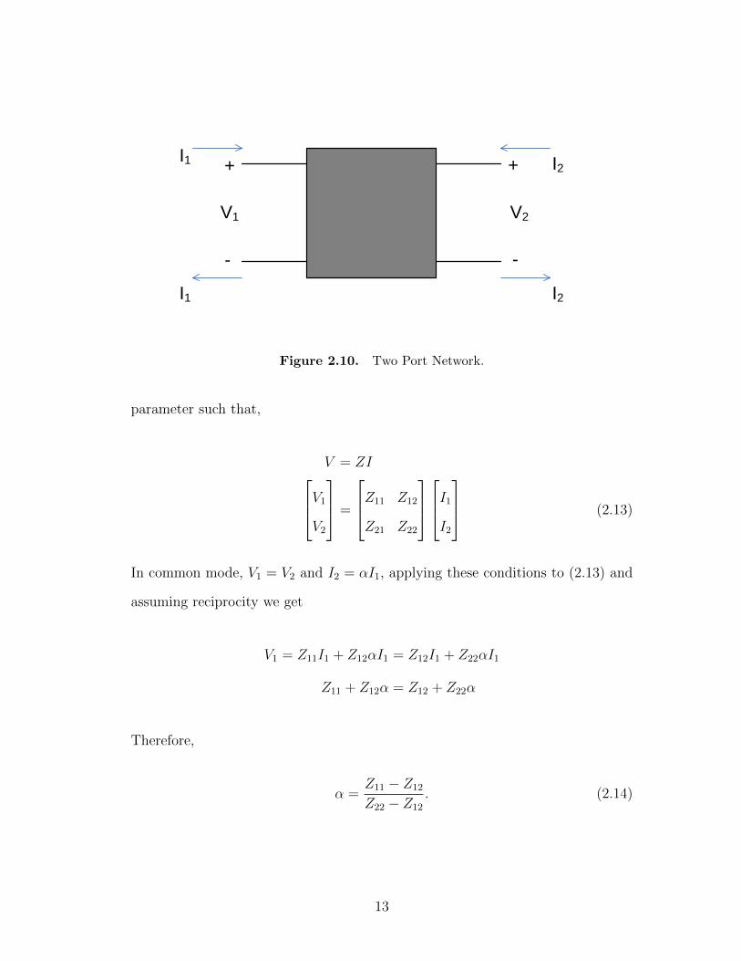
where a1 and a2 are unknown coefficients and c = (W1+W2+m+1)/4. Substitut-
ing (2.21) in (2.19), and finding the total charge using (2.20), α can be computed
as
α =Q2
Q1
=ln(4c+ 2[(2c)2 − (W1/2)2]1/2)− ln(W1)
ln(4c+ 2[(2c)2 − (W2/2)2]1/2)− ln(W2). (2.22)
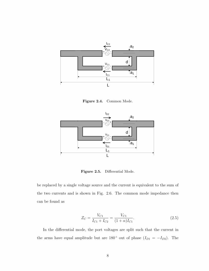
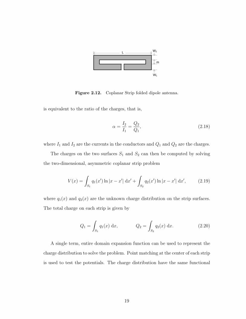
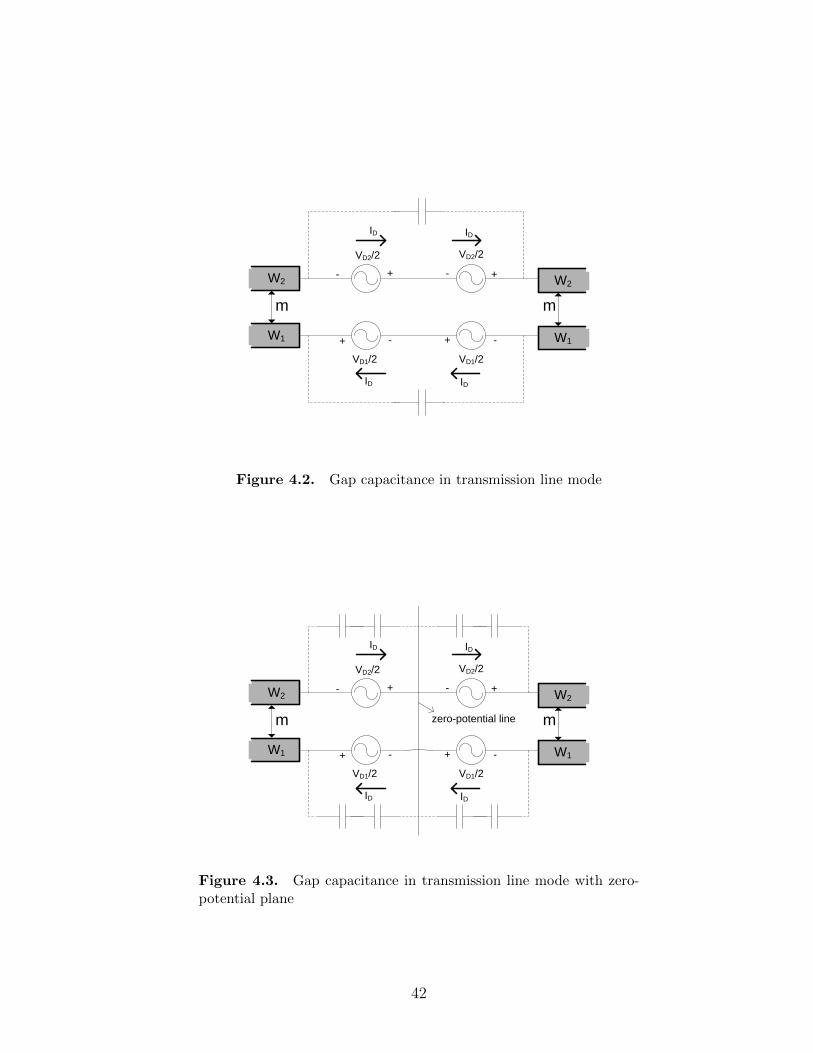
2.5.3 Differential Mode Impedance
Differential mode impedance, (ZD) for a strip dipole can be computed by con-
sidering Fig. 2.8 and (2.7). Visser [7], applied the wire Uda model to a Coplanar
strip (CPS) folded dipole antenna, shown in Fig. 2.12, and proposes improved
design equations to improve the accuracy of the model. The width of CPS dipole
considered in the paper is 5 mm (lies within the conversion bound), thereby,
King-Middleton second-order solution [22] is used to compute ZC by considering
an equivalent cylindrical dipole of radius ρe. The splitting factor α is computed
using (2.22). The characteristic impedance Z0 in (2.7), is computed assuming that
the dipole is a CPS in a homogeneous medium of relative permitivity εr and is
given by the (2.23) [24,25]
Z0 =120π√εr
K(k)
K ′(k), (2.23)
where K(k) is the complete elliptic function of the first kind and K ′(k) = K(k′),
where k′2 = 1− k2. The approximated complete elliptic function of the first kind
20
can be found in [7, 26].
The author found that when the strip dipole is placed in free space the com-
puted ZIN using wire Uda model follows the simulated ZIN near resonance. But
when the dipole is placed on a dielectric slab the accuracy of the model degrades.
This degradation is attributed to the computation of Z0 as the effect of dielectric
slab needs to be accounted for while computing Z0. The author shows that the
accuracy of the model improves when Z0 is computed assuming a symmetric CPS
on a dielectric slab of height h and relative permittivity εr. For a asymmetric
CPS with finitely thick substrate the expression for Z0 [27] is given as
Z0 =60π√εeff
K ′(k1)
K(k1), (2.24)
where
εeff = 1 + q(εr − 1)
q =1
2
K(k2)
K ′(k2)
K ′(k1)
K(k1),
k1 =
√W1
W1 +m
W2
W2 +m,
k2 =
√sinh (πW1/2h)
sinh (π(W1 +m)/2h)
sinh (πW2/2h)
sinh (π(W2 +m)/2h),
where m is the slot width.
The computation of ZIN using (2.7), (2.24), (2.22), and (2.12) constitutes the
strip dipole Uda model. This model can be used to analyze strip dipoles effectively.
In this section, a brief background of RFID technology was discussed. The
wire and strip dipole Uda model were defined. The introduced strip dipole Uda
21
model can be applied to T-match antenna and can be used to analyze UHF RFID
tag antennas. To find the simulated ZC , α and ZD, two port network analysis was
also discussed. The condition for maximum power transfer between the antenna
and the attached chip is also defined.
22
Chapter 3
Embedded T-Match Antenna
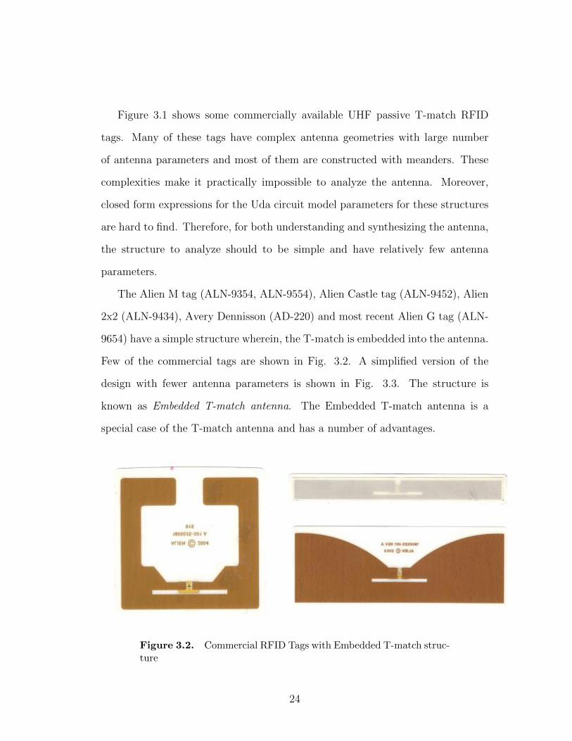
Figure 3.1. Commercial RFID Tags
23
Figure 3.1 shows some commercially available UHF passive T-match RFID
tags. Many of these tags have complex antenna geometries with large number
of antenna parameters and most of them are constructed with meanders. These
complexities make it practically impossible to analyze the antenna. Moreover,
closed form expressions for the Uda circuit model parameters for these structures
are hard to find. Therefore, for both understanding and synthesizing the antenna,
the structure to analyze should to be simple and have relatively few antenna
parameters.
The Alien M tag (ALN-9354, ALN-9554), Alien Castle tag (ALN-9452), Alien
2x2 (ALN-9434), Avery Dennisson (AD-220) and most recent Alien G tag (ALN-
9654) have a simple structure wherein, the T-match is embedded into the antenna.
Few of the commercial tags are shown in Fig. 3.2. A simplified version of the
design with fewer antenna parameters is shown in Fig. 3.3. The structure is
known as Embedded T-match antenna. The Embedded T-match antenna is a
special case of the T-match antenna and has a number of advantages.
Figure 3.2. Commercial RFID Tags with Embedded T-match struc-ture
24
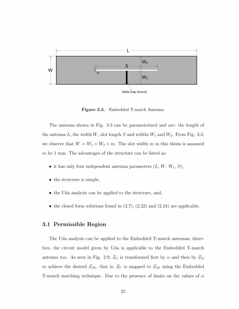
W
L
S
W1
W2
Delta Gap Source
m
Figure 3.3. Embedded T-match Antenna.
The antenna shown in Fig. 3.3 can be parameterized and are: the length of
the antenna L, the width W , slot length S and widths W1 and W2. From Fig. 3.3,
we observe that W = W1 + W2 + m. The slot width m in this thesis is assumed
to be 1 mm. The advantages of the structure can be listed as:
• it has only four independent antenna parameters (L, W , W1, S),
• the structure is simple,
• the Uda analysis can be applied to the structure, and,
• the closed form solutions found in (2.7), (2.22) and (2.24) are applicable.
3.1 Permissible Region
The Uda analysis can be applied to the Embedded T-match antennas, there-
fore, the circuit model given by Uda is applicable to the Embedded T-match
antenna too. As seen in Fig. 2.9, ZC is transformed first by α and then by ZD
to achieve the desired ZIN , that is, ZC is mapped to ZIN using the Embedded
T-match matching technique. Due to the presence of limits on the values of α
25
and ZD, there are certain ZC values which can be transformed to ZIN . To find all
possible ZC values which can be transformed by the Embedded T-match antenna
we propose to study the permissible region of the antenna, which is defined as
the ”set of all possible values the common mode impedance, ZC , can take, which
when transformed using a matching network yields the desired impedance”.
The permissible region of Embedded T-match antenna can be found by study-
ing the transformation of ZC to ZIN . The first transformation of ZC is by a linear
multiplier (1+α)2 and can be represented on Smith chart by a linear curve. Shunt
impedance, ZD transforms (1 +α)2ZC by moving along the constant conductance
arc on the Smith chart. The transformation of ZC depicting the steps is shown in
Fig. 3.4.
To find the permissible region, we need to invert (2.12) to compute ZC in terms
of ZIN , ZD and α. To achieve maximum power transfer ZIN = Z∗IC , where ZIC is
the impedance of the attached chip. Bounds are also defined in order to get the
permissible region.
Z∗IC =(1 + α)2ZCZD
(1 + α)2ZC + ZD. (3.1)
This can be re-written as
1
Z∗IC
=1
(1 + α)2ZC+
1
ZD(3.2)
The first bound on the permissible region can be found by taking α to be 0 and
varying ZD from 0 to∞ Ω. This bound is represented as ZAC and can be computed
26
ZC
ZIN
(1+α)2ZC
Figure 3.4. Embedded T-match network transformation on smithchart
as
1
Z∗IC
=1
ZAC
+1
ZD,
ZAC =
ZDZ∗IC
ZD − Z∗IC
. (3.3)
The second bound can be found by taking each value of ZAC and multiplying it
with (1 +αmax )2, where αmax is the maximum value α can take. Here, we assume
27
ZCA
ZCB
ZCC ZIC
*
Figure 3.5. Permissible region for Embedded T-match antennas
28
ZIC*
Figure 3.6. Permissible region area for Embedded T-match anten-nas
29
αmax to be 10. This bound is represented as ZBC and is given by
ZBC = (1 + αmax )−2ZA
C . (3.4)
Observing these bounds on the Smith chart we can then find the last bound by
taking ZD to be infinity and varying the value of α from 0 to αmax . Let the bound
be represented as ZCC and given by the expression
ZCC = (1 + αmax)
−2Z∗IC . (3.5)
The curves generated (ZIC = 14− j160 Ω) by ZAC , ZB
C and ZCC are shown in Fig.
3.5 and the area covered forms the permissible region for Embedded T-match
antennas and is shown in Fig. 3.6. The limits enforced on α and ZD are arbitrary.
3.2 Antenna Characteristics
To understand the Embedded T-match structure, experiments were conducted
wherein, the model parameters (L, W , W1 and S) were varied and the circuit
model parameters (ZC , α and ZD) were observed. Two port analysis was used
to compute the circuit model parameters, with the first port being placed on W1
arm and the second port on the W2 arm. The ports are constructed to replicate
delta gap sources and are shown in Fig. 3.7. The dipole antenna was placed in
free space and the frequency of operation was 915 MHz for all the experiments.
915 MHz was chosen as it is the center frequency of the Federal Communications
Commission (FCC) regulated frequency band for radio wave transmission in USA
and Canada.
Experiment 1
30
Port 1
L
WS
W1
Port 2
Figure 3.7. Two port analysis
In the first experiment, the effect of model parameters on ZC is studied. ZC , is
the input impedance of a center-fed dipole, therefore, it depends only on L and W
of the embedded T-match antenna. The dependence on L and W can be verified
by studying the following cases
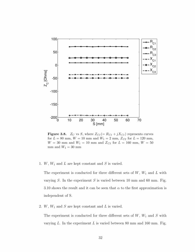
1. L, W and W1 are kept constant and S is varied.
Figure 3.8 shows the result of the experiment, wherein, three different sets
of L, W and W1 are used and S is varied between 10 mm to 60 mm for each
case. As can be seen ZC , is independent of S.
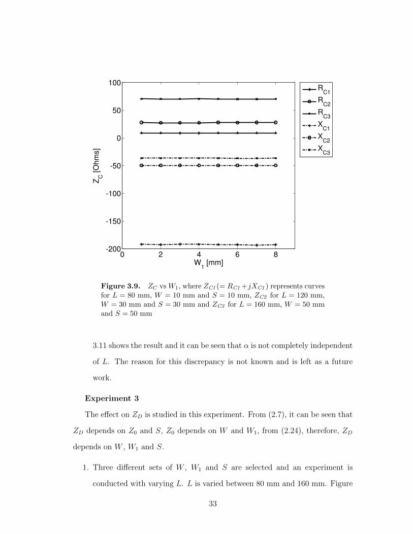
2. L, W and S are kept constant and W1 is varied.
In this experiment three different sets of L, W and S are used and W1 is
varied between 1 mm to 8 mm for each set. Figure 3.9 proves that ZC is
also independent of W1.
Experiment 2
The second experiment is conducted to observe the effect on model parameters
on α. From (2.22) it can be seen that α depends only on W and W1, this is further
verified by conducting the following experiments.
31
0 10 20 30 40 50 60 70-200
-150
-100
-50
0
50
100
S [mm]
ZC [
Oh
ms]
RC1
RC2
RC3
XC1
XC2
XC3
Figure 3.8. ZC vs S, where ZC1 (= RC1 + jXC1 ) represents curvesfor L = 80 mm, W = 10 mm and W1 = 2 mm, ZC2 for L = 120 mm,W = 30 mm and W1 = 10 mm and ZC3 for L = 160 mm, W = 50mm and W1 = 30 mm
1. W , W1 and L are kept constant and S is varied.
The experiment is conducted for three different sets of W , W1 and L with
varying S. In the experiment S is varied between 10 mm and 60 mm. Fig.
3.10 shows the result and it can be seen that α to the first approximation is
independent of S.
2. W , W1 and S are kept constant and L is varied.
The experiment is conducted for three different sets of W , W1 and S with
varying L. In the experiment L is varied between 80 mm and 160 mm. Fig.
32
0 2 4 6 8-200
-150
-100
-50
0
50
100
W1 [mm]
ZC [
Oh
ms]
RC1
RC2
RC3
XC1
XC2
XC3
Figure 3.9. ZC vs W1, where ZC1 (= RC1 +jXC1 ) represents curvesfor L = 80 mm, W = 10 mm and S = 10 mm, ZC2 for L = 120 mm,W = 30 mm and S = 30 mm and ZC3 for L = 160 mm, W = 50 mmand S = 50 mm
3.11 shows the result and it can be seen that α is not completely independent
of L. The reason for this discrepancy is not known and is left as a future
work.
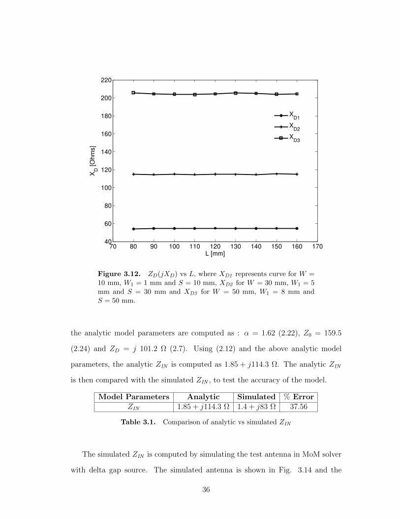
Experiment 3
The effect on ZD is studied in this experiment. From (2.7), it can be seen that
ZD depends on Z0 and S, Z0 depends on W and W1, from (2.24), therefore, ZD
depends on W , W1 and S.
1. Three different sets of W , W1 and S are selected and an experiment is
conducted with varying L. L is varied between 80 mm and 160 mm. Figure
33
0 10 20 30 40 50 60 701
1.5
2
2.5
3
3.5
4
S [mm]
α
α1
α2
α3
Figure 3.10. α vs S, where α1 represents curve for L = 80 mm,W = 10 mm and W1 = 1 mm, α2 for L = 120 mm, W = 30 mm andW1 = 5 mm and α3 for L = 160 mm, W = 50 mm and W1 = 8 mm.
3.12 shows the result of the experiment and proves that ZD is independent
of L.
From the experiments conducted it can summarized that to the first approxi-
mation
• ZC is a function of L and W ,
• α is a function of W and W1,
• ZD is a function of W , W1 and S for Embedded T-match antenna.
34
80 100 120 140 1600
0.5
1
1.5
2
2.5
3
L [mm]
α
α1
α2
α3
Figure 3.11. α vs S, where α1 represents curve for L = 80 mm,W = 10 mm and W1 = 1 mm, α2 for L = 120 mm, W = 30 mm andW1 = 5 mm and α3 for L = 160 mm, W = 50 mm and W1 = 8 mm.
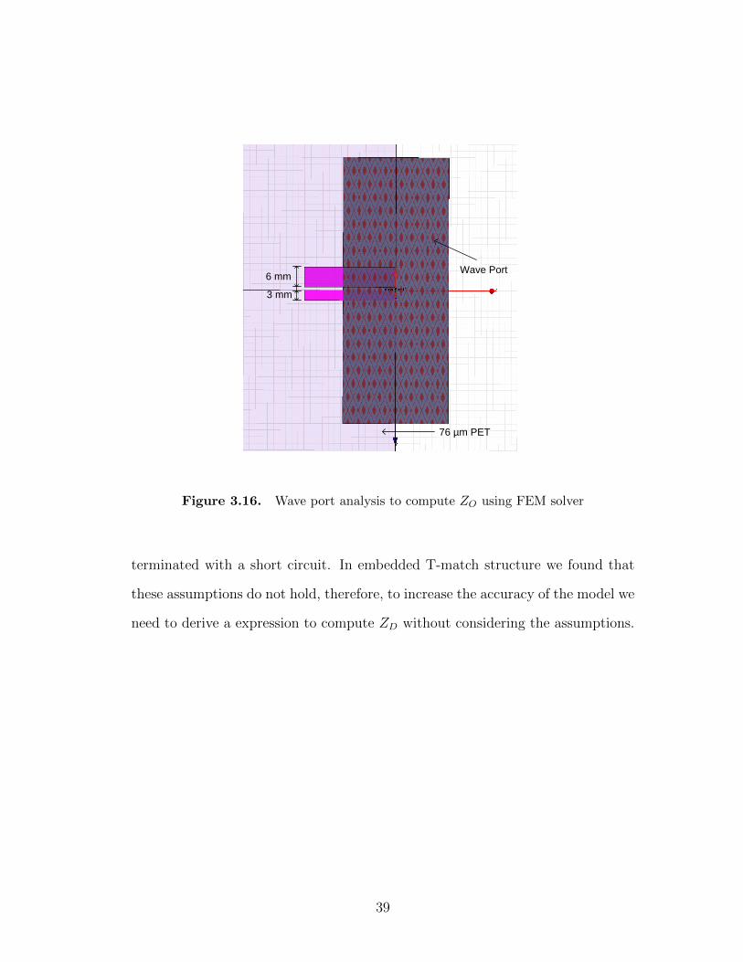
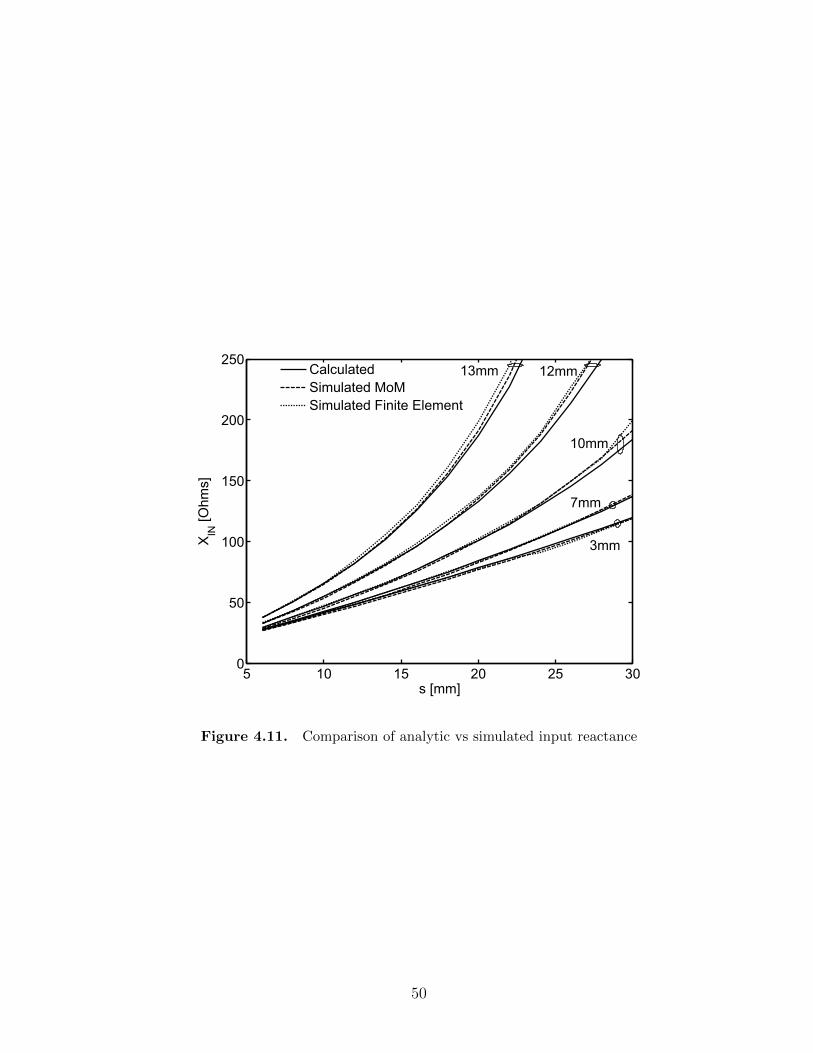
3.3 Accuracy of Strip Uda Model
The strip Uda model can applied to the structure to analyze the structure.
The accuracy of the model can be tested by computing ZIN , using the strip Uda
model and compare it with the simulated ZIN . The test antenna is placed on a
76 µm PET substrate (εr = 3.2), with 18 µ m copper used for the antenna and the
frequency of operation is 915 MHz. The test antenna parameters are : L = 100
mm, W = 10 mm, W1 = 3 mm, W2 = 6 mm and S = 20 mm.
A 100×10 mm center-fed rectangular antenna, shown in Fig. 3.13, is simulated
in MoM solver and yields a ZC of 15.64− j125.5 Ω. For the antenna parameters,
35
70 80 90 100 110 120 130 140 150 160 17040
60
80
100
120
140
160
180
200
220
L [mm]
XD
[O
hm
s]
XD1
XD2
XD3
Figure 3.12. ZD(jXD) vs L, where XD1 represents curve for W =10 mm, W1 = 1 mm and S = 10 mm, XD2 for W = 30 mm, W1 = 5mm and S = 30 mm and XD3 for W = 50 mm, W1 = 8 mm andS = 50 mm.
the analytic model parameters are computed as : α = 1.62 (2.22), Z0 = 159.5
(2.24) and ZD = j 101.2 Ω (2.7). Using (2.12) and the above analytic model
parameters, the analytic ZIN is computed as 1.85 + j114.3 Ω. The analytic ZIN
is then compared with the simulated ZIN , to test the accuracy of the model.
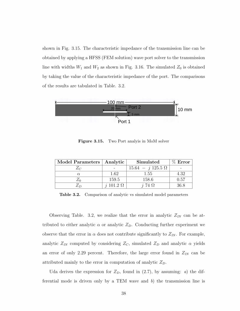
To validate the synthesis process an Embedded T-match antenna was designed
for Higgs 2 chip. The initial design constraints given are the: L = 100 mm,
W = 15 mm, and ZIC = 11 − j133 Ω (Higgs 2 chip). The tag is designed to
be placed on 76 µm PET substrate (εr = 3.2) with 18 µ m copper used for the
antenna and the frequency of operation considered is 915 MHz. For the given
L and W , the simulated ZC was found to be 14.5 − j101.3 Ω, using the MoM
solver. Using (5.10) and (5.11) we found αreq = 0.498 and ZDreq = j84.9 Ω. Using
bisection method and αreq value we get W1 and W2 to be 10.07 mm and 3.93 mm
54
respectively, analytic Z0 using (2.24) is found to be 146.9 Ω, Zp for the antenna
is found to be −j 350.7 Ω and XS = 4 Ω. From (5.18) we compute S value to
be 23.6 mm.
An antenna with the geometry obtained is simulated in MoM solver to compute
ZIN . The antenna parameters can be summarized as: L = 100 mm, W = 15 mm,
W1 = 10.07 mm and S = 23.6 mm. The antenna was simulated with delta gap
source and the simulated ZIN was found to be 10.8 + j127.8 Ω, which yields an
error of 3.9 percent from Z∗IC with τ = 0.9295 (−0.6350 dB).
55
Chapter 6
Conclusion
RFID technology is used to track and identify products/objects. Radio waves
are transmitted by a reader, RFID tag receives this signal (if in vicinity), the chip
on the tag modulates the signal and backscatters it to the reader with a unique ID.
UHF RFID passive tags are easy to fabricate and can be manufactured at low cost,
thereby, are being used in everyday life. Features, such as, read range, frequency of
operation, environment, bandwidth etc. drive the UHF passive RFID tag antenna
design. The tag antenna design can be expedited if the antenna characteristics are
known. To increase the read range of the UHF passive RFID tag, among others,
maximum power transfer between the chip and the antenna needs to be attained.
Uda analysis of wire T-match antenna helps in characterizing the antenna.
THe Wire dipole Uda model, which is applicable to wire dipole antennas, has
been modified by researchers for strip dipoles. The model proposed in this thesis
is defined as strip dipole Uda model. Commercial RFID tags are constructed
using strip dipoles because they are easy to fabricate and manufacture. Most of
the commercial UHF passive RFID tags are complex and are difficult to analyze.
The Embedded T-match antenna, which is special case of T-match antenna
56
is a simple antenna design with numerous advantageous. Uda analysis can be
applied to this structure for analysis. The permissible region for the Embedded
T-match antenna is also found and is seen to be limited by the maximum value α
and ZD can take. The strip dipole Uda model is applied to this structure and it is
found that the analytic ZIN has an error of more than 20 percent when compared
to the simulated ZIN . The error in analytic ZIN was found to be due to the
assumptions made while deriving the expression for ZD (2.7). Gap capacitance and
shunt inductance are introduced in the expression of ZD to improve the accuracy.
An augment Uda model for strip dipoles is defined with the new derived ZD
expression.
The accuracy of the model was tested and the error was found to be less than 2
percent. The augmented Uda model was validated by comparing the analytic ZIN
with the simulated ZIN found using the MoM and FEM solvers. The simplicity
of the Embedded T-match structure helps in using the augmented Uda model
to synthesize the antenna geometry. For a given chip impedance, L and W ,
embedded T-match can be constructed for maximum power transfer condition.
The synthesis process was also tested and was found to be accurate.
In conclusion the Uda model which is applicable to folded dipoles can be
extended to T-match antennas but with errors. The Embedded T-match antenna
which is a special case of T-match can be analyzed using the Uda model. The
proposed model increases the accuracy computing the input impedance of the
Embedded T-match antenna. The proposed model also helps in understanding,
analyzing and synthesizing the Embedded T-match antenna.
57
Chapter 7
Future Work
Since expressions to compute ZC are hard to find for fat dipoles, ZC is com-
puted using MoM solver, in this thesis. An expression to compute analytic ZC for
fat dipoles needs to be derived and used in the model to reduce the dependency on
the numerical tools and further reduce the time taken to design the tag antenna.
We also noticed small error in computation of analytic ZIN , this may be due to
presence of small RD (resistance associated with ZD). The error found can be
further reduced by computing ZIN by considering RD.
The permissible region for the Embedded T-match antenna was found by forc-
ing arbitrary limits on the maximum value α and ZD can take. Practical limits for
α and ZD need to be found to compute the permissible region. While studying the
characteristics of the Embedded T-match antenna, α was found to be dependent
on L. Observing (2.22), it can be seen that α depends mostly on W and W1.
Therefore, this discrepancy needs to be further examined and corrected.
The augmented Uda model was applied and tested at only one frequency (915
MHz). The application of the model at other frequencies can also be validated
and tested. The expansion of this model to other frequencies can help in deter-
58
mining the bandwidth of the antenna. The values for gap capacitance and shunt
inductance were obtained using curve fitting technique. A more rigorous analysis
can be conducted to derive the equations to compute the constants. This would
further simplify the analysis of the antenna.
The Uda analysis in this thesis is applied to a dipole Embedded T-match
antenna. As a future work one can apply the analysis to a microstrip Embedded
T-match antenna and test the accuracy of the model. The model can also be used
to study the effect of dielectric substrates on performance of Embedded T-match
antenna.
59
Appendix A
Antenna Characteristics
This appendix contains more results for experiment conducted in section 3.2.
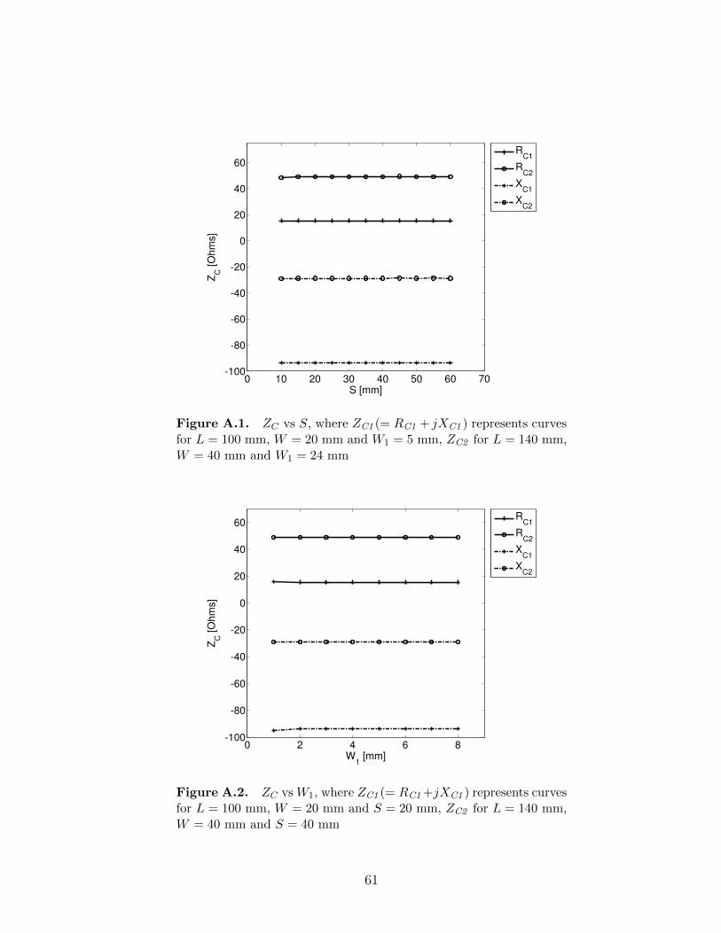
A.1 ZC vs. S and W1
Figure A.1 and A.2 shows the result of the experiment conducted for ZC for
varying S and W1 respectively. S is varied between 10 mm and 60 mm and W1 is
varied between 1 mm and 8 mm.
A.2 α vs. S and L
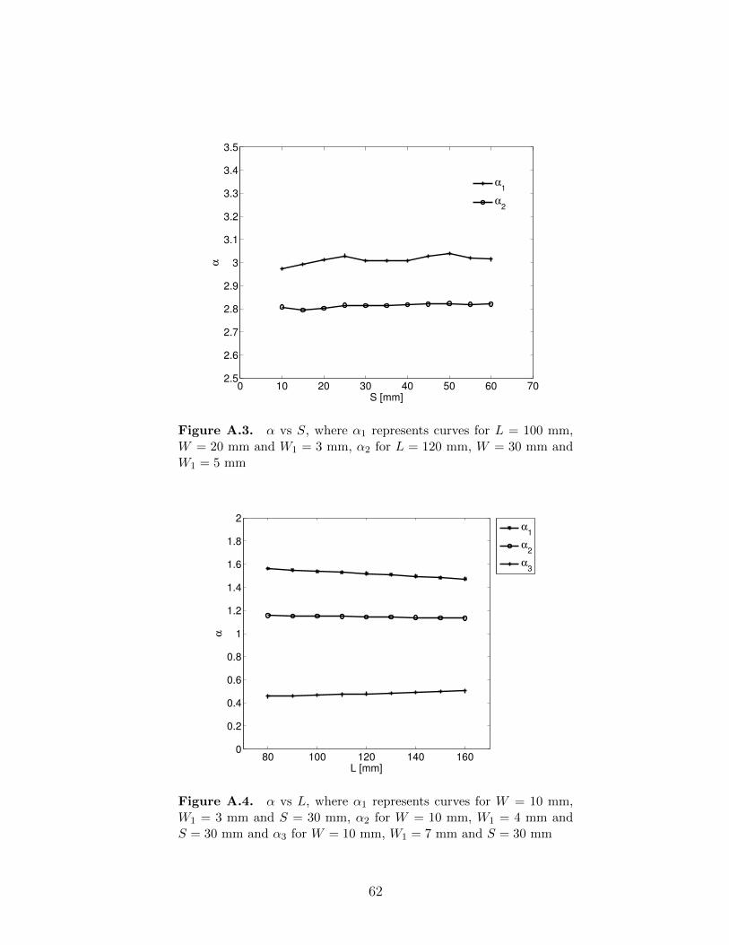
Figure A.3 and A.4 shows the result of the experiment conducted for α for
varying S and L respectively. S is varied between 10 mm and 60 mm and L is
varied between 80 mm and 160 mm.
60
0 10 20 30 40 50 60 70-100
-80
-60
-40
-20
0
20
40
60
S [mm]
ZC [
Oh
ms]
RC1
RC2
XC1
XC2
Figure A.1. ZC vs S, where ZC1 (= RC1 + jXC1 ) represents curvesfor L = 100 mm, W = 20 mm and W1 = 5 mm, ZC2 for L = 140 mm,W = 40 mm and W1 = 24 mm
0 2 4 6 8-100
-80
-60
-40
-20
0
20
40
60
W1 [mm]
ZC [
Oh
ms]
RC1
RC2
XC1
XC2
Figure A.2. ZC vs W1, where ZC1 (= RC1 +jXC1 ) represents curvesfor L = 100 mm, W = 20 mm and S = 20 mm, ZC2 for L = 140 mm,W = 40 mm and S = 40 mm
61
0 10 20 30 40 50 60 702.5
2.6
2.7
2.8
2.9
3
3.1
3.2
3.3
3.4
3.5
S [mm]
α
α1
α2
Figure A.3. α vs S, where α1 represents curves for L = 100 mm,W = 20 mm and W1 = 3 mm, α2 for L = 120 mm, W = 30 mm andW1 = 5 mm
80 100 120 140 1600
0.2
0.4
0.6
0.8
1
1.2
1.4
1.6
1.8
2
L [mm]
α
α1
α2
α3
Figure A.4. α vs L, where α1 represents curves for W = 10 mm,W1 = 3 mm and S = 30 mm, α2 for W = 10 mm, W1 = 4 mm andS = 30 mm and α3 for W = 10 mm, W1 = 7 mm and S = 30 mm
62
A.3 ZD vs. L
Figure A.5 shows the result of the experiment conducted for ZD for varying
L. L is varied between 80 mm and 160 mm.
80 100 120 140 16080
90
100
110
120
130
140
150
160
L [mm]
XD [
Oh
ms]
XD1
XD2
Figure A.5. ZD(jXD) vs L, whereXD1 represents curve forW = 20mm, W1 = 3 mm and S = 20 mm, XD2 for W = 40 mm, W1 = 7 mmand S = 40 mm.
63
Appendix B
Computation of Constants
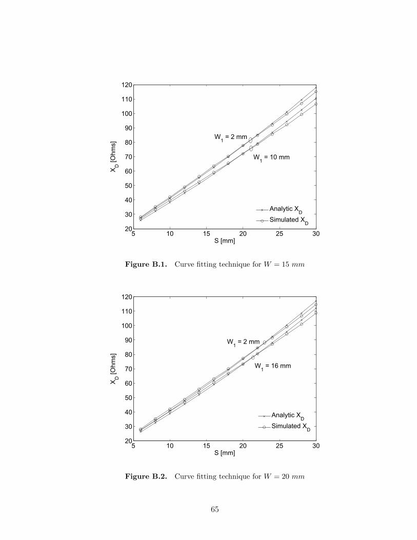
Figure B.1 and B.2 shows the curve fitting technique graph generated while
computing the constants Ci, Co and Xs for W = 15 mm and W = 20 mm
respectively.
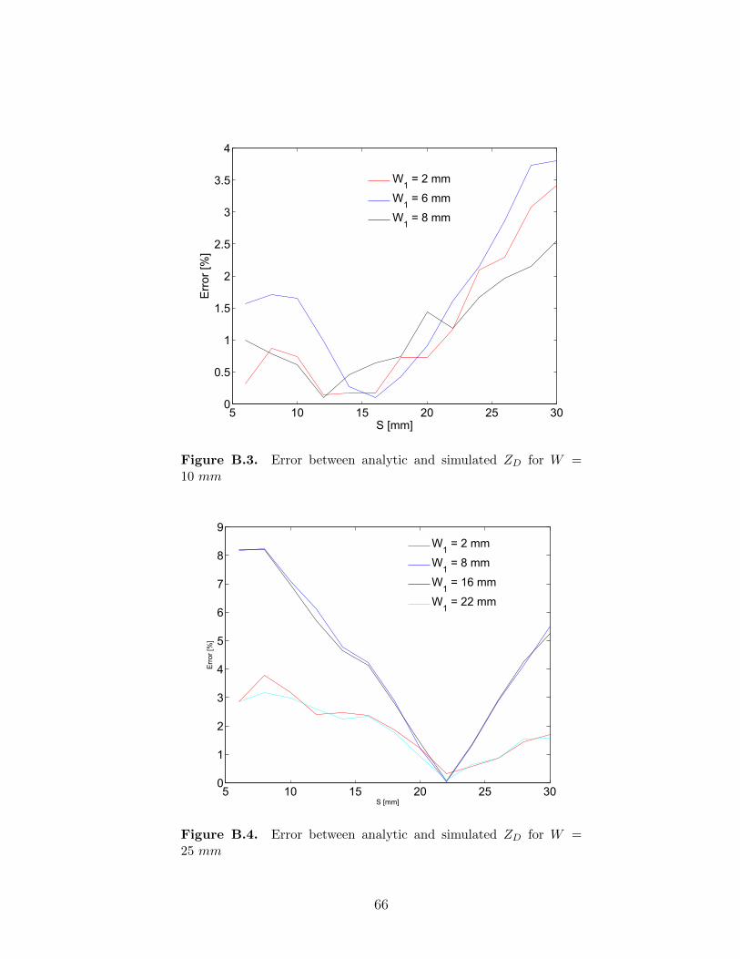
Figure B.3 and B.4 shows the error found between analytic and simulated ZD
for W = 10 mm and W = 25 mm respectively.
64
!
!
Figure B.1. Curve fitting technique for W = 15 mm
!
!
Figure B.2. Curve fitting technique for W = 20 mm
65
Figure B.3. Error between analytic and simulated ZD for W =10 mm
Figure B.4. Error between analytic and simulated ZD for W =25 mm
66
Appendix C
Derivation
In this appendix the derivation for ZDreq and αreq is shown.
Equation (5.6) can be re-written as
Y =−XICXDreq
XCXDreq +RCRIC +XCXIC
, (C.1)
substituting (C.1) in (5.7), we get
RICXDreq = Y (RCXDreq −RCXIC +RICXC), (C.2)
=
(−XICXDreq
XCXDreq +RCRIC +XCXIC
)(RCXDreq −RCXIC +RICXC). (C.3)
Solving for XDreq
−XICXDreqRC +RCX2IC −RICXCXIC = RICXCXDreq −RCR
2IC −RICXICXC ,
RC(R2IC +X2
IC ) = XDreq(RICXC +XICRC). (C.4)
67
The expression for XDreq is found to be
XDreq =RC(R2
IC +X2IC )
RICXC +XICRC
. (C.5)
Substituting (C.5) in (C.1)
Y =−XICRC(R2
IC +X2IC )
(RICXC +XICRC)(XC
RC(R2IC+X2
IC )
RICXC+XICRC−RCRIC −XICXC
) , (C.6)
=−XICRC(R2
IC +X2IC )
XCRCR2IC +XCRCX2
IC −RCR2ICXC −RICX2
CXIC −XICR2CRIC −X2
ICXCRC
.
(C.7)
=XICRC(R2
IC +X2IC )
RICX2CXIC +XICR2
CRIC
, (C.8)
=RC(R2
IC +X2IC )
RIC (R2C +X2
C). (C.9)
Therefore, αreq and ZDreq can be computed as
αreq =
√RC(R2
IC +X2IC )
RIC (R2C +X2
C)− 1, (C.10)
ZDreq = jXD = −j RC(R2IC +X2
IC )
RCXIC +RICXC
. (C.11)
68
References
[1] Daniel M. Dobkins. The RF in RFID: Passive UHF RFID in Practice.
Newnes, 2007.
[2] G. Marrocco. The Art of UHF RFID Antenna Design: Impedance-Matching
and Size-Reduction Techniques. In IEEE Antennas and Propagation Maga-
zine, volume 50, pages 66–79, 2008.
[3] P. V. Nikitin and K. V. Seshagiri Rao and S. F. Lam and V. Pillai and R.
Martinez and H. Heinrich. Power Reflection Coefficient Analysis for Com-
plex Impedances in RFID Tag Design. In IEEE Transactions on Microwave
Theory and Techniques, volume 53 NO. 9, pages 3870–3876, 2005.
[4] S. Uda and Y. Mushaike. Yagi-Uda Antenna. Sasaki Printing and Publishing
Co., 1954.
[5] C. A. Balanis. Antenna Theory Analysis and Design: 3rd Edition. John
Wiley & Sons Inc., 2005.
[6] G. A. Thiele and E. P. Ekelman and L. W. Henderson. On The Accuracy of
the Transmission Line Model of the Folded Dipole. In IEEE Transactions on
Antennas and Propagations, volume AP-28, No. 5, pages 700–703, 1980.
69
[7] H. J. Visser. Improved Design Equations for Asymmetric Coplanar Strip
Folded Dipoles on a Dielectric Slab. In Antennas and Propagation Interna-
tional Symposium, 2007.
[8] C. T. Tai. Theory of Terminated Monopole. In IEEE Transactions on An-
tennas and Propagation, pages 408–410, 1984.
[9] J. Choo and J. Ryoo and J. Hong and H. Jeon and C. Choi and M. M.
Tentzeris. T-Matching Networks for the Efficient Matching of Practical RFID
Tags. In European Microwace Conference, pages 5–8, 2009.
[10] K. Kurokawa. Power Waves and the Scatttering Matrix. In IEEE Transac-
tions on Microwave Theory and Technique, volume 13 No. 3, pages 194–202,
1965.
[11] R. W. Lampe. Design Formulas for an Asymmetric Coplanar Strip Folded
Dipole. In IEEE Transactions on Antennas and Propagation, pages 1028–
1031, 1985.
[12] R. W. Lampe. Corrections to: Design Formulas for an Asymmetric Coplanar
Strip Folded Dipole. In IEEE Transactions on Antennas and Propagation,
page 611, 1986.
[13] L. Brillouin. Origin of Radiation Resistance. In Radioelectricite, pages 147–
152, 1922.
[14] A. A. Pistolkors. Radiation Resistance of Beam Antennae. In Proceedings
IRE, pages 562–579, 1929.
[15] P. S. Carter. Circuit Relations in Radiating Systems and Applications to
Antenna Problems. In Proceeding IRE, pages 1004–1041, 1932.
70
[16] R. E. Burgess. Aerial Characteristics. In Wireless Engr., volume 21, pages
154–160, 1944.
[17] J. D. Kraus. Antennas. McGraw-Hill, New York, 1988.
[18] R. Bechmann. On the Calculation of Radiation Resistance of Antennas and
Antenna Combinations. In Proceedings IRE, volume 19, pages 461–466, 1931.
[19] H. E. King. Mutual Impedance of Inequal Length Antennas in Echelon. In
IRE Transactions Antennas and Propagation, volume AP-5, pages 306–313,
1957.
[20] J. E. Storer. Variational Solution to the PRoblem of the Symmetrical Cylin-


![Antennas and Propagation in UHF RFID Systems · RFID systems with a range of several meters appeared in early 1970’s [3]. Since then, RFID has significantly advanced and experienced](https://static.documents.pub/doc/80x56/5e520aaba589531fe25e271e/antennas-and-propagation-in-uhf-rfid-systems-rfid-systems-with-a-range-of-several.jpg)

