IEEE TRANSACTIONS ON CIRCUITS AND SYSTEMS, VOL. 37, NO. 2, FEBRUARY 1990 183 Analysis of a Hybrid Analog/Switched-Capacitor Phase-Locked Loop Abstract -A hybrid analog/switched-capacitor phase-lockedloop (PLL), henceforth referred to as the hybrid phase-locked loop (HPLL) is pre- sented. It consists of a switched-capacitor (SC) loop filter and an analog voltage-controlled oscillator (VCO). The HPLL is unique because it combines building blocks which are both discrete and continuous time in nature. The primary advantages offered by this particular PLL implemen- tation are its amenability to monolithic integration, inherently low phase noise compared to standard SC implementations and potential for high frequency operation. This paper contains a detailed analysis of the HPLL. Nonlinear state descriptions of the first- and second-order HPLL’s are obtained which are suitable for deterministic analyses. The locations of steady-state equilibrium operating points are given, along with relevant stability conditions. Also, a small signal model for loops of arbitrary order is presented. The behavior of the HPLL for random inputs is also treated, where the input consists of a sinusoid plus random Gaussian noise. Both linear and nonlinear analyses are presented. The results of the analyses performed are substantiated by both computer simulation and laboratory measurements on a discrete prototype. The analyses given here are directly applicable to standard SC PLL’s, for which no comprehensive analysis has previously been performed. Thus the results presented here are useful for systems designers using all SC PLL’s as well as the HPLL. I. INTRODUCTION HE phase-locked loop (PLL) has become an impor- T tant building block In a wide range of applications [1]-[5]. For this reason, monolithic realizations of the PLL are highly desirable for minimization of space, weight, and power requirements. In addition, monolithic integrated circuits enjoy a reliability advantage over their hybrid or discrete counterparts. The ideal monolithic PLL is area efficient and requires no off-clup components. A device with these features would have applications in telecommu- nications for functions such as tone decoding and in digital signal processing for synchronization of processor timing to a sampling strobe. The use of MOS switched-capacitor (SC) circuits in the realization of PLL circuits has also been discussed in the literature [6]-[ll]. However, most of the PLL circuits using SC subcircuits involve the use of SC voltage-controlled oscillators (VCO’s) which exhibit rela- tively large phase noise. Those that do not typically make use of off chip components to set the PLL parameters. In this paper, a PLL architecture is described and ana- lyzed which has the potential of meeting the goals de- Manuscript received March 17, 1988; revised March 27, 1989. This D. Asta is with the MIT Lincoln Laboratory, Lexington, MA 02173. D. N. Green is with Hughes Aircraft Company, Building S12, Los IEEE Log Number 8932872. paper was recommended by Associate Editor C.A.T. Salama. Angeles, CA 90009. scribed above and can be implemented in MOS technol- ogy. This PLL architecture will henceforth be referred to as the hybrid phase-locked loop (HPLL). The HPLL is shown here to exhibit a fundamental behavior inherently different than any previously studied. The difference be- tween the HPLL and conventional PLL‘s is due to its structure as a hybrid of both continuous- and discrete-time components. In this paper the behavior of the HPLL is modeled and discrete-time state descriptions are derived for first- and second-order loops. Next, small-signal stabil- ity and acquisition (transient analysis) are addressed. Fi- nally, the stochastic behavior of the HPLL under noisy input conditions is analyzed using both small- and large- signal models. The results of the analyses presented are verified by experiments on a laboratory prototype and computer simulations. As discussed below, the analysis of the HPLL is compli- cated by the presence of nonlinear terms which do not appear in the analysis of either continuous- or discrete-time PLL‘s. While the analysis proceeds in a manner similar to that previously used for a digital PLL [13], a more general technique is used to account for the nonlinear terms. It should also be noted that all analyses presented here for the HPLL hold for standard SC PLL’s under the assump- tion that the clock frequency is large compared to the frequency of operation. 11. THE HYBRID PHASE-LOCKED LOOP The HPLL represents a basic departure from digital or continuous time analog PLL‘s. The details of the basic implementation and mathematical model of the HPLL are presented in tlus section. Fig. 1 describes the HPLL in block diagram form. The loop input is modeled here as a continuous-time sinusoid with amplitude A and frequency w. The phase is an arbitrary time function, f3(t). The loop operates by track- ing the zero crossings of the input waveform. The phase detection operation is performed by an analog sampler. The output of the sampler is shown in this section to be a sinusoidal function of the phase difference between the input waveform and the waveform controlling the sampler (ignoring the effect of noise). The remainder of the HPLL consists of a sampled-ana- log SC loop filter driving an analog voltage-controlled oscillator (VCO). Herein lies a unique feature of the HPLL 0098-4094/90/0200-0183$01.00 01990 IEEE
Transcript
IEEE TRANSACTIONS ON CIRCUITS AND SYSTEMS, VOL. 37, NO. 2, FEBRUARY 1990 183
Analysis of a Hybrid Analog/Switched-Capacitor Phase-Locked Loop
Abstract -A hybrid analog/switched-capacitor phase-locked loop (PLL), henceforth referred to as the hybrid phase-locked loop (HPLL) is pre- sented. It consists of a switched-capacitor (SC) loop filter and an analog voltage-controlled oscillator (VCO). The HPLL is unique because it combines building blocks which are both discrete and continuous time in nature. The primary advantages offered by this particular PLL implemen- tation are its amenability to monolithic integration, inherently low phase noise compared to standard SC implementations and potential for high frequency operation. This paper contains a detailed analysis of the HPLL. Nonlinear state descriptions of the first- and second-order HPLL’s are obtained which are suitable for deterministic analyses. The locations of steady-state equilibrium operating points are given, along with relevant stability conditions. Also, a small signal model for loops of arbitrary order is presented. The behavior of the HPLL for random inputs is also treated, where the input consists of a sinusoid plus random Gaussian noise. Both linear and nonlinear analyses are presented. The results of the analyses performed are substantiated by both computer simulation and laboratory measurements on a discrete prototype. The analyses given here are directly applicable to standard SC PLL’s, for which no comprehensive analysis has previously been performed. Thus the results presented here are useful for systems designers using all SC PLL’s as well as the HPLL.
I. INTRODUCTION HE phase-locked loop (PLL) has become an impor- T tant building block In a wide range of applications
[1]-[5]. For this reason, monolithic realizations of the PLL are highly desirable for minimization of space, weight, and power requirements. In addition, monolithic integrated circuits enjoy a reliability advantage over their hybrid or discrete counterparts. The ideal monolithic PLL is area efficient and requires no off-clup components. A device with these features would have applications in telecommu- nications for functions such as tone decoding and in digital signal processing for synchronization of processor timing to a sampling strobe. The use of MOS switched-capacitor (SC) circuits in the realization of PLL circuits has also been discussed in the literature [6]-[ll]. However, most of the PLL circuits using SC subcircuits involve the use of SC voltage-controlled oscillators (VCO’s) which exhibit rela- tively large phase noise. Those that do not typically make use of off chip components to set the PLL parameters.
In this paper, a PLL architecture is described and ana- lyzed which has the potential of meeting the goals de-
Manuscript received March 17, 1988; revised March 27, 1989. This
D. Asta is with the MIT Lincoln Laboratory, Lexington, MA 02173. D. N. Green is with Hughes Aircraft Company, Building S12, Los
IEEE Log Number 8932872.
paper was recommended by Associate Editor C.A.T. Salama.
Angeles, CA 90009.
scribed above and can be implemented in MOS technol- ogy. This PLL architecture will henceforth be referred to as the hybrid phase-locked loop (HPLL). The HPLL is shown here to exhibit a fundamental behavior inherently different than any previously studied. The difference be- tween the HPLL and conventional PLL‘s is due to its structure as a hybrid of both continuous- and discrete-time components. In this paper the behavior of the HPLL is modeled and discrete-time state descriptions are derived for first- and second-order loops. Next, small-signal stabil- ity and acquisition (transient analysis) are addressed. Fi- nally, the stochastic behavior of the HPLL under noisy input conditions is analyzed using both small- and large- signal models. The results of the analyses presented are verified by experiments on a laboratory prototype and computer simulations.
As discussed below, the analysis of the HPLL is compli- cated by the presence of nonlinear terms which do not appear in the analysis of either continuous- or discrete-time PLL‘s. While the analysis proceeds in a manner similar to that previously used for a digital PLL [13], a more general technique is used to account for the nonlinear terms. It should also be noted that all analyses presented here for the HPLL hold for standard SC PLL’s under the assump- tion that the clock frequency is large compared to the frequency of operation.
11. THE HYBRID PHASE-LOCKED LOOP The HPLL represents a basic departure from digital or
continuous time analog PLL‘s. The details of the basic implementation and mathematical model of the HPLL are presented in tlus section.
Fig. 1 describes the HPLL in block diagram form. The loop input is modeled here as a continuous-time sinusoid with amplitude A and frequency w . The phase is an arbitrary time function, f3( t ) . The loop operates by track- ing the zero crossings of the input waveform. The phase detection operation is performed by an analog sampler. The output of the sampler is shown in this section to be a sinusoidal function of the phase difference between the input waveform and the waveform controlling the sampler (ignoring the effect of noise).
The remainder of the HPLL consists of a sampled-ana- log SC loop filter driving an analog voltage-controlled oscillator (VCO). Herein lies a unique feature of the HPLL
0098-4094/90/0200-0183$01.00 01990 IEEE
184 IEEE TRANSACTIONS ON CIRCUITS AND SYSTEMS, VOL. 37, NO. 2, FEBRUARY 1990
OUTPUT
Fig. 1. HPLL block diagram.
REALIZED WITH MOS DEVICES
. . . . . . . . ,
SHUNT CLAMP
- Fig. 2. Sampler/clamp combination for first-order loop.
. SHUNT CLAMP
I I _ _ I SAMPLEANDHOLD I
I _ _ _ _ _ _ _ _ _ _ J
Fig. 3. Sampler/loop filter combination for second-order loop.
structure. In analog PLL's, the VCO continuously re- sponds to changes in the controlling voltage. In this case, however, the controlling voltage changes only at discrete- time instants. This is similar to the case of digital and standard SC PLL's, but the signal period of both those types of PLL's is limited to a discrete set of values, resulting in potentially severe quantization errors.
111. MODELING THE HPLL It is assumed in the derivations below that transients
that occur due to clocking or signal sampling decay rapidly relative to the clock period. It is further assumed that the sampler/loop filter combination provides an output which is a function of the input signal only at the clock instants and is otherwise constant throughout the clock period. Under these assumptions, the HPLL can be accurately modeled by discrete time difference equations. These as- sumptions are standard in the analysis of SC networks.
The sampler/loop filter combination to be analyzed for the first-order loop is shown in Fig. 2. Ths circuit provides the necessary features for use in the HPLL and exhibits a zeroth-order transfer function characterized by a linear
gain, G, , equal to unity. Other circuits are possible which allow other values of G , to be realized. However, a wide range of loop parameter values can be acheved by varying the signal input amplitude, A , or by varying the VCO characteristic.
The implementation of the sampler/loop filter combina- tion for the second-order loop to be considered is shown in Fig. 3. The sample/hold circuit could be repositioned ahead of the integrator section without affecting loop operation or the analysis. The shunt clamp (or limiter) ideally acts as an open circuit when the voltage impressed across it lies within the interval [U,,,, U,,] and acts other- wise as a short circuit. The clamp serves to limit VCO frequency excursions, thereby avoiding ambiguous locking behavior. This ambiguous locking behavior is referred to herein as subharmonic locking and is treated in greater detail below. It should be noted that the clamp is necessary regardless of the loop order. The filter output voltage, U( k ) is the voltage that appears at the output just after the kth rising edge of clock phase 9,.
The operational amplifiers are assumed ideal, allowing the circuit to be analyzed via charge conservation equa- tions. The result is as follows: U( k ) = S [ U( k - 1 ) + ( G , + G , ) x ( k ) - G,x( k - l ) ] (1)
where
urnax, X ' ~ , ,
U m n , X < U m n
S [ x ] = x , U," < X =G U , , (2 )
G , = - C1/C2 (3) (4)
i and
G , = - C, /C3. The limiter characteristic S [ . ] in (2) above accounts for the action of the shunt clamp. This limiter characteristic is not the only one that permits analysis to proceed, but is easily analyzed and is a close approximation to physically realiz- able circuits.
The analog VCO is modeled as having a general, memo- ryless voltage-to-frequency characteristic and a static rest frequency, U,,, when the input voltage is zero. Defining the VCO output phase as +,(t), this relationship is expressed as follows:
-- d 9 0 ( t ) - 0, + g( u ( t ) ) . dt ( 5 )
By noting that the VCO completes one cycle whenever 2m radians of phase is accumulated, the following is obtained from (5):
277 t , - t,-,=
a, + g( U ( k - 1 ) )
where 2 a
0,
T A - 0
ASTA AND GREEN: HYBRID ANALOG/SC PLL 185
is the rest period of the VCO, t k is the time corresponding to the beginning of the kth VCO cycle and u ( k ) is the loop filter output in the time interval [ t k , t k + l ) . Taking to to be zero it then follows that
and the result for the second-order loop is
+( k ) = +( k - 1) - 2au (U( k - 1))
U@) = s [ U( k -1) + ( G , + G * )
+ e(+ e ( k -1) (16)
. ( A sin (+( k - 1 ) - 2au ( U( k -1)) (7)
k - l S ( U ( j ) )
j = o WO + g ( . ( j ) ) *
t k = kT, - To 1
Now define + e ( k ) - e ( k - ~ ) + ~ ( k ) )
- G,( A sin+( k - 1) + n ( k - l))] . (17) It is convenient in many cases to deal with the modular phase error, +,, = +mod( - a, a]. In terms of +,,, the state description of the first-order loop becomes
(8) g ( x )
0, + g ( x ) . U(.) A
It will henceforth be assumed that U(.>, and thus g ( . ) are strictly increasing and have derivatives which are uni- formly bounded between 0 and ca. These assumptions are quite valid for practical VCO designs. In terms of U( e ) , (7) +,,( k ) = [ +,,( k - 1) takes the following form:
k - 1 - 2au ( S [ G,( A sin+,,( k - 1 ) + n ( k - I ) ) ] )
.. -
t k = k T , - T o u(u(~)). (9 ) + e & ) - e ( k - , ) ] mod( - a , ~ ] (18) j = O
and the result for the second-order loop is
+ , , ( k ) = [ + T ( k - l ) - 2 a u ( U ( k - l ) ) Equation (9) illustrates the inherently nonlinear relation- ship between the loop filter output, u ( k ) , and the Sam- pling times t , . The relationship is nonlinear even when the VCO characteristic, g ( . ) , is linear. This is in contrast to the equation used by Weinberg and Liu in analyzing the nonuniform sampling digital PLL [13].
The loop filter equations (eq. (1) for the second-order HPLL filter) can be combined with (9) to derive a state variable description for the HPLL. In deriving this model the signal input to the loop, x ( t ) , is assumed to have the form:
x ( t ) = A sin ( w,t + 8 ( t ) ) + n ( t ) .
(19) + 8 ( k ) - 0 ( k - l ) ] mod ( - a , a]
U( k ) = S [U( k - 1) + ( G , + G2)
( A sin ( +T( k - 1) - 2au ( U( k - 1 ) )
+ e( k ) - e( k - 1))) + .( k ) )
- G,( A sin+,,( k - 1 ) + n ( k - l))] . (20)
The state equations given above are the basis of the (10) analysis to follow.
Before leaving this section, a final point should be made In this expression, e( t ) , represents phase modulation of the input signal, 0, is the rest frequency of the VCO in radians per second and n ( t ) is zero-mean, white Gaussian
‘Oncemi% the modeling Of sc pLL‘s. Under the approxi- mation that the Operating is much less than the clock frequency, virtually all SC VCO’s described in the literature have operating characteristics identical to those assumed here for continuous time VCO’s. Hence, the state descriptions given above and all subsequent analyses apply
noise with variance U,‘. Any constant frequency offset between the input and is lumped into e ( t ) . Equations (9) and (10) can now be combined to yield
.~
i k - 1
x ( t k ) =Asin e ( t k ) - 2 a 1 u ( u ( j ) ) + n ( t , ) (11)
where t , is the time when the rising edge of clock phase +, occurs. Define the following:
i j = O
e( k ) e( t , ) (12)
n ( k ) & n ( t k ) (13)
+ ( k ) ~ e ( k ) - 2 ~ 1 + ( j ) ) . (14) k - 1
j = O
State descriptions for the first- and second-order loops can be derived from the loop filter equations and (11) following the procedure described in [12]. For the first- order loop the result is
to standard SC PLL‘s in addition to the HPLL. The approximation regarding the clock frequency is standard in analyzing such circuits. Since no detailed analysis of SC PLL‘s has previously been presented, the results given here provide an analysis tool useful for this class of circuits.
IV. LOCKING BEHAVIOR AND SMALL-SIGNAL ANALYSIS
Small-signal linear analysis for HPLL is useful for studying steady-state equilibrium behavior and stability properties under these same conditions. Throughout this section, the HPLL input phase, 8 ( t ) , is assumed to have the following form:
e ( t ) = Aw,t + @ + f J ( t ) , t > 0. (21)
In this expression A is a constant less than unity, Aw, is the offset between the input frequency and the V,CO rest frequency, @ is an arbitrary constant phase and e ( t ) is a “small” signal. In this context “small” means that the
+ ( k ) = + ( k -1) - 2 a u ( s [ G l ( A s i n + ( k - 1 ) + n ( k - 1 ) ) 1 )
+ e(+ e ( k -1) (15)
186 IEEE TRANSACTIONS ON CIRCUITS AND SYSTEMS, VOL. 31. NO. 2, FEBRUARY 1990
linearized difference equations presented below are valid. The input described by (21) is the most complex form which can be tracked by first- and second-order loops and still yield a static steady-state equilibrium.
First-Order Loop Phase locking, or locking, refers to the achievement of
steady-state behavior in the absence of noise. Setting O ( t ) to zero in (21) and using the definition of U ( -) yields
I9( k ) - 8( k - 1) = 27~A(l- U ( U( k - 1)) ) . (22) Substituting this result into (18) produces
+,, ( k ) = [ +,,( k - 1) + ~ T A - 27~( 1 + A )
. U ( S [ G,A sin+,,( k - l)] )] mod ( - .rr, 771. (23)
Denote the steady-state value of +,, as k + 00 by +,,,,. It follows from (23) that +,,,, can be any value within the interval (- T, T ] such that for some integer n E { O , l , 2, - . . } the following relation holds:
There may be many solutions of (24) corresponding to different values of n . If solutions exist for values of n other than zero, subharmonic locking can occur. When t h s happens, the steady-state VCO frequency equals an integer submultiple of the input frequency. If a particular solution to (24) is n = n o and the HPLL input frequency is U,, then the loop can lock with a steady-state VCO frequency equal to a , / ( n 0 + 1). This behavior is most dangerous when solutions exist for multiple values of n. When this occurs, the locking behavior of the loop is ambiguous in the sense that the steady-state frequency of the VCO is indetermi- nate. To prevent this ambiguous form of subharmonic locking, the VCO frequency excursion must be limited so that only one solution to (24) exists for the expected range of input frequencies. Analysis shows that the best way to limit the VCO excursion is to limit the voltage range of the loop filter output. Without loss of generality it is assumed throughout the remainder of this paper that the VCO excursion is appropriately limited so that only the n = 0 solution exists in (24).
Another problem with subharmonic locking can occur when multiple inputs are present at the HPLL input. If one of the input signals has an integer submultiple which lies in the constrained VCO frequency range, then the HPLL may lock to this integer submultiple of said input. To prevent such behavior, filtering may be employed at the loop input to reject the offending signals. To completely avoid potential problems with subharmonic locking, it is necessary to both constrain the VCO frequency excursion and filter the input spectrum to reject frequencies for which undesired subharmonic locking may occur.
As stated above, it is assumed throughout the remainder of this paper that only the n = 0 solution to (24) exists, corresponding to locking at the fundamental input fre- quency. In order for this solution to exist the following
condition is placed on the VCO control voltage (i.e., loop filter output) limits, urnin and uma:
If this equation is satisfied, then the following equation must have a solution in order for steady state to exist:
G,A sin ( +,,,,) = U-' - (1 :A)
When both (25) and (26) are satisfied, there are two solutions to (24) for n = 0:
where the range of sin-'( .) is taken to be [ - 7r/2,77/2]. As long as the steady-state loop filter output is not at one of the clamped limits, (23) can be linearized about the equi- librium points to determine stability properties.
The necessary condition for asymptotic stability near an equilibrium point is
Since cos( +,,,,) and cos(+,,,,,) have opposite signs, only one of the solutions given in (27) can be stable. Using the method described in [12], it is concluded from (28) that (+,,,,,) is the stable solution when G , A > 0, while (+,,mZ) is stable when G,A > 0.
Second- Order Loop Following the procedure described in [12], the second-
order loop is shown to have two equilibrium points gven by
+,,,,=o, or 7T. (30) In deriving these results it is assumed that u ( k ) is appro- priately clamped to prevent subharmonic locking. As for the first-order loop, only one of these equilibrium points can be stable. The conditions which produce a stable equilibrium are
sgn(G,) = sgn(G2) (31) n
where
a = - 2 ~ ( 1 + Ad( . , ) ) . (34)
Further, +,,,, = 0 is the stable operating point when G,A > 0, while +,,w = 7~ is the stable point when G,A < 0. It has been shown [12] that when one equilibrium point is a
ASTA AND GREEN: HYBRID ANALOG/SC PLL 187
stable operating point, the remaining unstable equilibrium is a saddle point; i.e., one eigenvalue lies outside the unit circle and the other lies inside. The stability results pre-
and digital PLL‘s.
Small-Signal Model - Arbitrary Order Loop Filter
conditions the one-sided transforms are well defined:
(44)
(45)
O( z ) = Acos ( + J H ( z )&( z )
& ( z ) = 6 ( z ) - & o ( z ) sented here are analogous to those for second-order analog
2r(1+ A ) u ’ ( u , ) z - l
1- z-l &&) = C(z). (46)
A small signal model is valid near stable equilibrium points as described above. The model allows for a loop filter of arbitrary order. As before, the HPLL phase input is assumed to be that given by (21).
The VCO phase, Go(/?), is defined as follows: k -1
+ & ) = 2 r c U(U(d). (35) j = - ,
Thus
= w- (36)
It is assumed that + and u*have stable steady-state values for the input of (21) yhen t9 is zero; i.e., the loop is locked. Then, for “small” d ( t ) , the HPLL behavior is modeled near equilibrium by a linear set of equations in the small signal variables 4 and a. Combining the two above equa- tjons and linearizing yields the following result in terms of + and a:
(37)
where & ( k ) is the small-signal VCO phase given by k - 1
r$o(k) = 2 n ( l + A)u’(u,) i(j). (38)
A general linear loop filter is assumed whch is com- pletely described by its discrete-time impulse response, h ( k ) . Using (11) and (14), x ( k ) can be expressed by
j = O
x ( k ) = Asin+(k)+ n ( k ) . (39) Under small-signal conditions,
2 ( k ) h x ( k ) - x ( +m) = A cos ( +,,,) 4 ( k ) + n ( k ) . (40)
Mainiaining small-signal operation requires that both n( k ) and 8 ( k ) are small. Small n ( k ) in this case means a high signal-to-noise ratio (SNR) at the loop input. Combining the above results produces the following small-signal model:
~ ( k ) = ( k ) * (Acos(+rm)4(k) + n ( k ) ) (41)
4 ( k ) = w4- 4 m (42)
~ o ( k ) = 2 r ( l + A ) u ’ ( ~ m ) C i ; ( j ) . (43) k - 1
j - 0
The noise n ( k ) in (41) is addressed in Sections V-VI1 of this paper, which treat the stochastic analysis of the HPLL. For deterministic analysis the noise is set to zero and a frequency-domain representation is obtained by taking z-transforms of the above equations. Under small-signal
Using (44)-(46), transfer functions from the input to any point in the loop are derived via straightforward algebra:
1- z- l -- & ( z ) -
m - 6 ( z ) 1 - z + 2 TA (1 + A ) COS ( +,,, ) U’( U,) z - ‘H( z )
(47)
A (1 + A ) COS ( @,,,) (1 - z - ’ ) H ( z ) 1 - zY1 + 2rA( 1 + A ) COS ( +vm) U’( U,) Z - ‘H( z )
-- 6 ( z )
(48)
2rA (1 + A ) cos ( +,,m) U’( urn) z- lH( z ) - - 1 - z - + 2 TA ( 1 + A ) COS ( +,,, ) U’( U, ) z - lH( z ) ’
(49)
The transfer function HJz) relates the VCO phase spec- trum to the input phase spectrum. Note that H,(ej”) = 1. For the HPLL to be stable, the complex zeros of the denominator in (47)-(49) must lie inside the unit circle in the complex plane.
V. MODELING THE HPLL FOR STOCHASTIC ANALYSIS Equations (15)-(20) are valid for simulation, determina-
tion of steady state operating points, transient analysis and small-signal analysis. However, there are two considera- tions that must be accounted for in the stochastic model- ing ot the HPLL. First, the variable + is nonstationary in the steady state. Due to cycle slipping, the variance of + grows with time. However, it has been shown [12] that the modular phase +,, = [+]mod( - T, 771 is stationary in the steady state and can be used as one of the state variables of a second-order state description. Similarly, a first-order loop can be modeled using +,, as the single state variable. The second issue that must be dealt with in the case of the second-order loop is that the state variable U is not Markov. This is indicated by the presence of both n ( k ) and n ( k - 1) on the right-hand-side of (17) and (20). Matters are further complicated by the presence of the nonlinear saturation function S [ -1.
This and the following two sections of this paper deal with the behavior of the HPLL with random inputs. The first step in this analysis is to obtain a state description of the HPLL in terms of a state vector which is both Markov and asymptotically stationary.
The derivation of the Markov state equation for the second-order loop begins by first considering the loop
188 IEEE TRANSACTIONS ON CIRCUITS AND SYSTEMS, VOL. 37, NO. 2, FEBRUARY 1990
Fig. 4. Flow diagram representation of the loop filter equation.
filter equation, repeated here for convenience:
~ ( k ) = S [ U ( k -1) +(GI + G,)x(k) - G,x(k -1)] (50) where S [ -1 is the limiter characteristic discussed above. Equation (50) is exactly represented by the flow diagram shown in Fig. 4. In this diagram an alternate variable, v is introduced to describe the loop filter. The relationship between v and U is given by
~ ( k ) = S [ ~ ( k - l ) ] -Glx(k- l ) . (51) A second-order state description in terms of v is then given by
+( k ) = +( k - 1) TU( S [ V( k - 1) + (GI + G2)
( A sin+(k - 1) + n ( k - I ) ) ] )
+e(+ e ( k - 1 ) (52)
. ( A sin+( k - 1) + n( k - I ) ) ]
- G,( A sin+( k - 1) + n ( k - 1)) .
V( k ) = S [ Y( k - 1) + ( Gl + G2)
(53) Using the variables +,, and v rather than + and U, the second-order state equations (52) and (53) become:
+,,(IC) = [ +,,(k - 1) TU( S [ ~ ( k - 1) + (G, + G2)
. ( A sin+,,( k - 1) + n ( k -
+ 8 ( k ) - O(k -l)] mod(
v ( k ) = S [ ~ ( k - l ) + (Gl + G2)
( A sin+,,( k - 1) + n( k -
. G , ( A s i n + , ( k - l ) + n ( k - l ) ) . (55) The vector [A, VI' is Markov, and thus (54) and (55) can be used to perform nonlinear stochastic analysis.
The modular state equation for the first-order loop presented previously, (18) is expressed in terms of the single state variable +,,, which is both Markov and asymp- totically stationary. Hence, this state description is suitable for nonlinear stochastic analysis without further modifica- tion. This equation is repeated here for convenience:
+,,(I?) = [+, , (k -l)-2mu(S[Gl(Asin+,,(k -1)
+ n ( k - l))] ) + e( k ) - e( k - l)] mod ( - T, T] . (56)
The small-signal behavior of the HPLL with random inputs is considered in the next section. This type of
analysis is useful when the signal-to-noise ratio at the input is large.
VI. SMALL-SIGNAL ANALYSIS If the signal-to-noise ratio at the HPLL input (SNR,) is
large and there is an absence of large transients, then small signal linear analysis is sufficient to assess the loop behav- ior. To begin th s analysis consider the input waveform given by
x ( t ) = A sin ( o,t + e ( t )) + n ( t ) . (57) Here n( t ) is stationary Gaussian noise with zero mean and standard deviation U,. The noise n ( t ) is usually generated by circuits prior to the PLL. The phase e ( t ) accounts for any constant frequency offset between the input frequency and the VCO rest frequency, U,. Under small-signal condi- tions, the sampled amplitude noise n ( k ) appears as an equivalent input phase noise, denoted by e,( k ) . These two variables are related by [14], [U]:
where 8, is also zero-mean, stationary and Gaussian. The average signal power at the loop input, P,, is equal to A2/2. Thus the input signal-to-noise ratio, SNR, is given
(59)
Combining the above relationships yields 1
These expressions are identical to those applicable to the analog PLL under identical conditions [15]. The power spectrum of the phase noise is given by
where P+" +" and Po,@, are the VCO and input phase noise spectra, r&p"ectively, and the sampling period T is consid- ered constant. The VCO phase noise variance is given by
where H, is the transfer function relating 6 to 6, as given by (49) and restated below:
2 TA ( 1 + A ) cos ( +,,m ) U'( U, ) z - 'H( z ) 1 - 2 - l - t ~ T A (1 + A ) COS ( +,,m) U'( urn) z-~H( z ) '
- -
(63)
Of special interest is the important case where n ( k ) (and hence 8,(k)) is white. For this case,
Pone,( e'"'') = O ~ T . (64)
ASTA AND GREEN: HYBRID ANALOG/SC PLL 189
Under this special condition (62) becomes
T U&= ~t-ln/~ IHo(e'"T)12do. ( 6 5 ) 27l - w / T
Defining the one-sided loop noise bandwidth, B,, by
equation (65) then becomes
Equation (67) is again analogous to results obtained for analog PLL's [15].
Further clarification is warranted regarding the sam- pling time T used in the equations of this section. As already discussed, the HPLL is a nonuniform sampling device. That is, there is no constant sampling period per se, since the input signal is sampled and the output signal is produced at nonuniform time intervals. However, under the small signal conditions assumed throughout this section, the sampling intervals will only deviate slightly from the average value of l/fsig, where fsi, is the signal frequency. This average value is the value of T used in the equations presented in this section.
VII. NONLINEAR STOCHASTIC ANALYSIS The large-signal behavior of the HPLL under noisy
conditions is treated in this section. The analysis is based on the theory of discrete-time Markov random processes. This approach allows investigation of several key behav- ioral aspects of the HPLL: the joint probability density function (PDF) of the state variables as a function of k, the asymptotic stationarity of this joint PDF as k + 00
and cycle slipping behavior. In principle, an arbitrary order loop can be analyzed
using the techniques employed in this section. However, first- and second-order loops are most often used. For this reason, attention is focused on these two cases. The HPLL input is assumed to be the sum of a phase and frequency step; this is the highest order input waveform that can be tracked by first- and second-order loops and yield a static steady-state equilibrium condition.
For analyzing asymptotic steady-state properties, the modular phase error variable +,, is used. This is necessary, since the nonmodular phase error + is not stationary in the steady state. When analyzing cycle slipping, however, the nonmodular phase error must be used.
The primary goals of the analysis to follow are to obtain the asymptotically stationary joint PDF of the two state variables +,, and U, and the mean number of cycles to first slip (MCFS). The joint PDF is important in that it con- tains the information necessary to statistically characterize the HPLL behavior. The MCFS is the average number of cycles elapsed before the first cycle slip occurs when start- ing from the steady-state operating point. Viterbi [16] extensively analyzed this parameter for analog PLLs.
Weinberg and Liu [13] analyzed the MCFS of the first- order digital PLL using iterative techniques. Cycle slipping is important in applications where the PLL is used to establish an absolute time or phase reference point relative to an incoming signal. The MCFS provides a figure of merit for comparing the performance of particular loop designs.
The First-Order Loop The analysis of the first-order loop begins with the
modular state description given in (56). The specific input under consideration is given by
e( t ) = AwoT + 'P, t >, 0 . (68)
With this input, (56) becomes
+,, (k) = [ +,, (k - 1) + 21~A - 2 ~ ( l + A )
. u ( S [ G,( A sin&( k - 1) + n (k - l))] )]
. m o d ( - l r , ~ ] . (69) The corresponding equation in terms of the nonmodular phase error is
+(k) =+(k -1) +2vA - 2 ~ ( l + A )
. U ( S [GI( A sin+( k - 1) + n ( k - l))]). (70) The state variables +,, and + are both Markov. A funda- mental relationship governing the behavior of Markov processes is the Chapman-Kolmogorov equation. For the first-order loop and the variable cpT, this equation is
The limits of integration in (71) span the entire range of +-. The transition density function q is invariant with k, since the system is time invariant. Given the initial PDF po, the stochastic behavior is uniquely specified for all k > 0.
The existence of a unique steady-state PDF p(+,,) has been established [12]. An equation for p(+,,) can be ob- tained from (71) by letting k + 00. In the steady-state, (71) becomes
P ( + J = /7r 4(+*lY1)P(Yl) 4 1 . (72) -7r
The steady-state density function p is the solution to (72). One way to solve this equation is to assume an initial distribution po and iterate using (71) until a steady-state conditionis reached, regardless of the choice of po. How- ever, a "good guess" will require less iterations.
When the HPLL is operating under noisy conditions, the nonmodular phase error + occasionally crosses _+ 77.
When this occurs, the modular phase +* "wraps around" from - 77 to 77 or from -77 to - 77. This effect must be accounted for in determining the transition density q. Fig. 5 illustrates the wraparound effect. Fig. 5(a) depicts the case where y1 is near zero, and no wraparound occurs. In Fig. 5(b), y , is nearer to -77, and wraparound does occur. The spikes in the figure denote Dirac delta functions, which account for the action of the clamp in the loop filter. The extent of the wraparound region is determined by y,, U,, and urnin. If urnin and U,, are chosen large enough, the function may wrap back on itself two or more times. However, this would represent a poor design where subharmonic locking could occur. In other words, the loop would be ill posed in this case.
Analysis of (69) yields the following expression for q [12]:
00 1 q(+TIYl) = 2-77(1 + A ) c W b Y A
I = - m
where
- Asin y1 yl - +,, + 2 TA + 2 -771
277(1+ A ) X / ( + , , , Y l ) A - - U - l
d d/(+,,, y,) A -u-'(y>, evaluated at
dY
A y , + 277A - 2-77 (1 + A ) U ( U,,) +Umu
+mumm [ mod ( - 77, -771.
The function N,, is the PDF of a zero-mean normal random variable with variance U:, while Q is the probabil- ity distribution corresponding to N. when U. = 1.
190 IEEE TRANSACTIONS ON CIRCUITS AND SYSTEMS, VOL. 31, NO. 2, FEBRUARY 1990
- " - +/
I I I
0
Y, t :I,-- ''
(b)
occurring. (b) Wraparound occurring. Fig. 5. Illustration of circular waraparound effect. (a) No wraparound
The transition density for the nonmodular phase vari- able, q(+lyl), is arrived at by similar means:
1 1 y 1 - + + 2 r A q(+'yl) = 2-77(1+ A)G, N+( G, 2 4 1 + A ) )
Equations (73) and (74) can be used to directly calculate the iterates p k in (71). However, an algorithm has been described in [12] which allows the iterates to be calculated without direct evaluation of the above expressions. This algorithm is also applicable to second-order loops.
A careful inspection of (73) and (74) under small-signal conditions (small U,) reveals that the transition density does in fact become Gaussian, as expected. Under the small-signal assumption, the second and third terms in these equations become negligble, while the derivatives, d,, are constant. Further, only one term of the summation in (73) is nonzero. Thus, the transition density reduces to a Gaussian form.
A derivation of the MCFS can proceed based on the above results. The method used is essentially that used in [13]. The derivation yields the result that
MCFS =I + J+;/P(+) - d+ (75)
where P(+) is the solution to the following integral equa- tion:
ASTA AND GREEN: HYBRID ANALOG/SC PLL 191
and k +, are the phase boundaries at whch a cycle slip is NO CLAMPING ACTION
I'
. <I>-
declared. The value of +/ is normally taken to be m, which is the case for all results presented herein.
The Second-Order Loop The analysis of the second-order loop proceeds in a
manner similar to that for the first-order loop. For the
state equations, (54), and (55), become frequency step plus phase step input, (68), the modular tx \ - I
+, ( k ) = [ +71 ( k - 1) + 2mA - 277 (1 + A )
. U( S [ V( k -1) +(GI + G2)
. ( A sin +,, ( k - 1) + n ( k - I))] )] mod( - m, m] (77)
Fig. 6. Graph of locus on which transition density q is defined. V( k ) = S [ V( k - 1) + ( Gl + G 2 )
. ( A sin+,,( k - 1) + n ( k -I))] For studying cycle slipping, the nonmodular version of (81) is needed. This equation is
p k ( + 7 1 ,
- G,( A sin+*( k - 1) + n( k - 1)). (78) Similarly, the nonmodular state equations (52) and (53), become - m - m
vo) = Jm Jm q(+71, Y 2 )
+ ( k ) = + ( k - l ) + 2 n A . P R - l ( Y l > Y2l+TO, vo ) dYldY2. (83)
-2m(1+ A ) u ( S [ v ( k - 1) + ( G l + G2)
. ( ~ s i n + ( k - l ) + n ( k - l ) ) ] )
In evaluating the MCFS for the second-order loop it is assumed that the initial state is the equilibrium point for a noiseless input. The derivation is an extension of that for the first-order loop. Define
(79)
~ ( k ) = S [ ~ ( k - 1) + (G, + G 2 ) 00
P(+> 4 = c P , h 4 (84) ( A sin+( k - 1) + n ( k - I))] - G l ( A sin+( k - 1) + n ( k - 1)). J =1 (80)
The existence of a unique steady-state PDF P ( + ~ , v ) has been established in [12]. The behavior of the iterates p k are analyzed via the vector Chapman-Kolmogorov equa- tion: equation:
where the conditioning notation has been dropped, since it is implicitly assumed. A derivation employing (83) [I21 reveals that P( +, Y) is the solution to the following integral
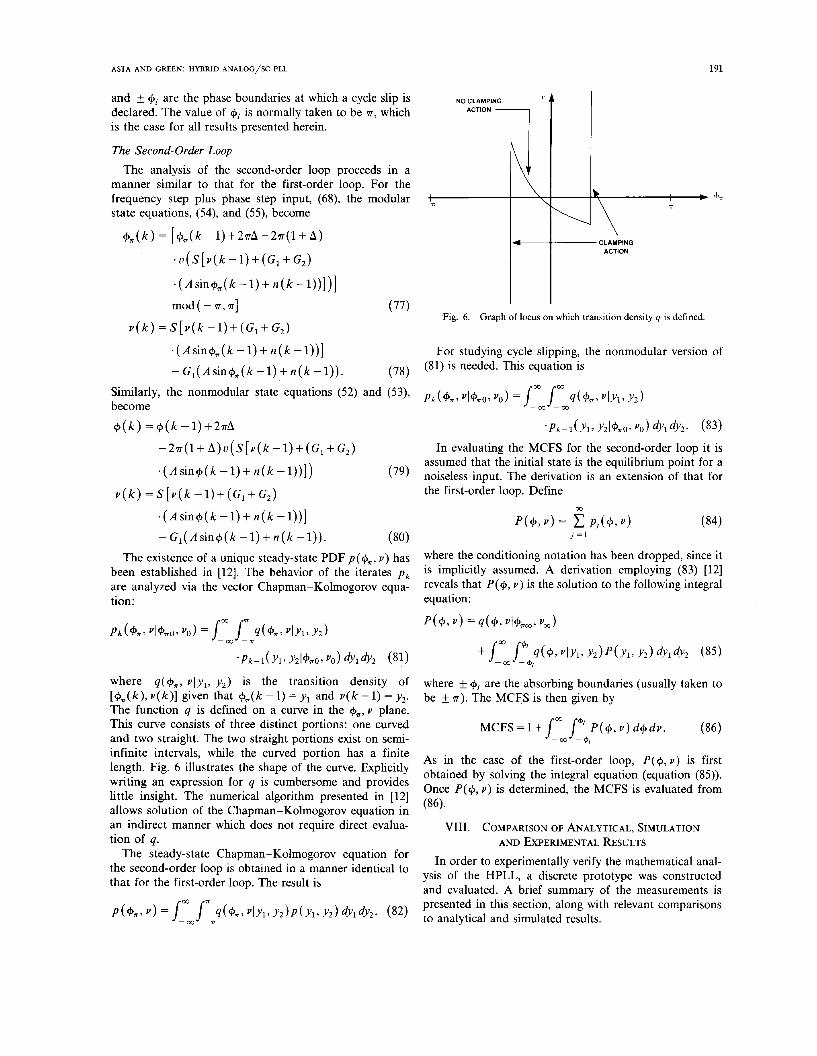
where q(&, vIyl, y2) is the transition density of [+,,(k), v(k)] given that +,,(k - 1) = y , and v ( k - 1) = y2. The function q is defined on a curve in the +,,, v plane. This curve consists of three distinct portions: one curved and two straight. The two straight portions exist on semi- infinite intervals, while the curved portion has a finite length. Fig. 6 illustrates the shape of the curve. Explicitly writing an expression for q is cumbersome and provides little insight. The numerical algorithm presented in [12] allows solution of the Chapman-Kolmogorov equation in an indirect manner whch does not require direct evalua- tion of q.
The steady-state Chapman-Kolmogorov equation for the second-order loop is obtained in a manner identical to that for the first-order loop. The result is
where f +I are the absorbing boundaries (usually taken to be f m). The MCFS is then given by
MCFS=l+Jpm So' P ( + , v ) d + d v . (86)
As in the case of the first-order loop, P(+, v ) is first obtained by solving the integral equation (equation (85)). Once P(+, v) is determined, the MCFS is evaluated from (86)-
m -0,
VIII. COMPARISON OF ANALYTICAL, SIMULATION AND EXPERIMENTAL RESULTS
In order to experimentally verify the mathematical anal- ysis of the HPLL, a discrete prototype was constructed and evaluated. A brief summary of the measurements is
192
Parameter GI G,
IEEE TRANSACTIONS ON CIRCUITS AND SYSTEMS, VOL. 37, NO. 2 , FEBRUARY
/ - - - - I
First Second ' Order Loop Order Loop
1 0.475 0 0.215 V
. FIRST ORDER
.. SECOND ORDER
- v'ss
Fig. 7. Schematic of prototype HPLL.
RA 1 160K
TABLE I COMPONENTS USED IN HPLL CIRCUIT.
(a) ACTIVE DEVICES. (b) PASSIVE COMPONENTS; CAPACITANCES
I N p F , RESISTANCES IN Q I DEVICE 1 MFK. 1 M F R . P.4R'Y
160K
(4
I COMP. I FIRST-ORDER I SECOND-ORDER 1
RB 1.1M 1.1M
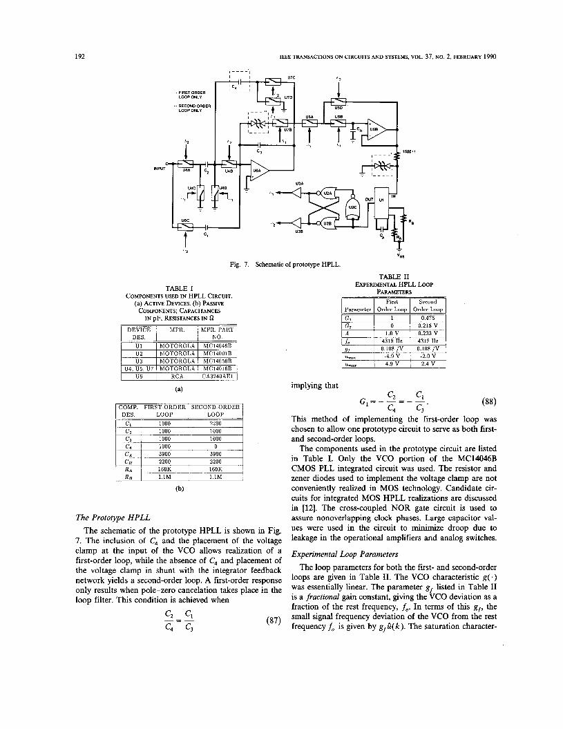
The Prototype HPLL The schematic of the prototype HPLL is shown in Fig.
7. The inclusion of C4 and the placement of the voltage clamp at the input of the VCO allows realization of a first-order loop, while the absence of C, and placement of the voltage clamp in shunt with the integrator feedback network yields a second-order loop. A first-order response only results when pole-zero cancelation takes place in the loop filter. This condition is achieved when
(87) c2 c, c4 c3
=- -
implying that
This method
4318 Hz 4318 Hz 0.108 /v 0.108 /v
U,in -4.9 v -2.0 v U,..."- 4.9 v 2.4 V
1990
(88) c2 c, c4 c3 *
G - - - = - - 1-
of implementing the first-order loop was chosen to allow one prototype circuit to serve as both first- and second-order loops.
The components used in the prototype circuit are listed in Table I. Only the VCO portion of the MC14046B CMOS PLL integrated circuit was used. The resistor and zener diodes used to implement the voltage clamp are not conveniently realized in MOS technology. Candidate cir- cuits for integrated MOS HPLL realizations are discussed in [12]. The cross-coupled NOR gate circuit is used to assure nonoverlapping clock phases. Large capacitor val- ues were used in the circuit to minimize droop due to leakage in the operational amplifiers and analog switches.
Experimental Loop Parameters The loop parameters for both the first- and second-order
loops are given in Table 11. The VCO characteristic g ( - ) was essentially linear. The parameter g, listed in Table I1 is a fractional gain constant, giving the VCO deviation as a fraction of the rest frequency, f , . In terms of this g,, the small signal frequency deviation of the VCO from the rest frequency f, is given by g,O(k). The saturation character-
ASTA AND GREEN: HYBMD ANALOG/SC PLL 193
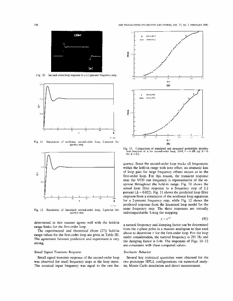
(4 Fi 9 Small signal transient response of first-order loop. (a) Nominal
=0, 7 = 204 ps. (b) Nominal A = 0.081, 7 = 399 ps (c) Nominal A = 0.102, T = 984 ps. (b)
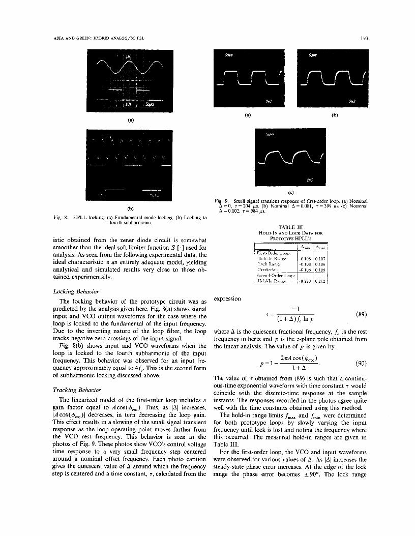
fourth subharmonic. Fig. 8. HPLL locking. (a) Fundamental mode locking. (b) Locking to
istic obtained from the zener diode circuit is somewhat smoother than the ideal soft limiter function S [ - 1 used for analysis. As seen from the following experimental data, the ideal characteristic is an entirely adequate model, yielding analytical and simulated results very close to those ob- tained experimentally.
Locking Behavior
The locking behavior of the prototype circuit was as predicted by the analysis given here. Fig. 8(a) shows signal input and VCO output waveforms for the case where the loop is locked to the fundamental of the input frequency. Due to the inverting nature of the loop filter, the loop tracks negative zero crossings of the input signal.
Fig. 8(b) shows input and VCO waveforms when the loop is locked to the fourth subharmonic of the input frequency. This behavior was observed for an input fre- quency approximately equal to 4f0. This is the second form of subharmonic locking discussed above.
Tracking Behavior The linearized model of the first-order loop includes a
gain factor equal to Aces(+,,,,). Thus, as /A1 increases, IA cos ( r&,m) I decreases, in turn decreasing the loop gain. This effect results in a slowing of the small signal transient response as the loop operating point moves farther from the VCO rest frequency. This behavior is seen in the photos of Fig. 9. These photos show VCO's control voltage time response to a very small frequency step centered around a nominal offset frequency. Each photo caption gives the quiescent value of A around whch the frequency step is centered and a time constant, T, calculated from the
TABLE I11 HOLD-IN AND LOCK DATA FOR
PROTOTYPE HPLL's I
I An,,, 1 Amer I First-Order Loop:
Lock Raiigc Prediction
Second-Order Loop:
expression - 1
where A is the quiescent fractional frequency, f, is the rest frequency in hertz and p is the z-plane pole obtained from the linear analysis. The value of p is given by
(90) 2m4 cos (&)
p = l - l + A '
The value of 'T obtained from (89) is such that a continu- ous-time exponential waveform with time constant T would coincide with the discrete-time response at the sample instants. The responses recorded in the photos agree quite well with the time constants obtained using this method.
The hold-in range limits f,, and fmin were determined for both prototype loops by slowly varying the input frequency until lock is lost and noting the frequency where this occurred. The measured hold-in ranges are given in Table 111.
For the first-order loop, the VCO and input waveforms were observed for various values of A. As lAl increases the steady-state phase error increases. At the edge of the lock range the phase error becomes k90". The lock range
194 IEEE TRANSACTIONS ON CIRCUITS AND SYSTEMS, VOL. 37, NO. 2, FEBRUARY 1990
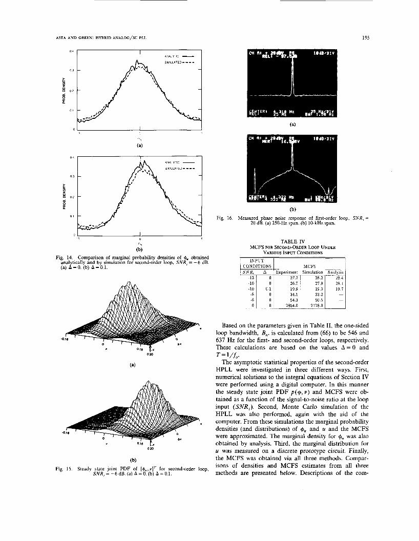
Fig. 10. Second-order loop response to a 2.2-percent frequency step.
determined in this manner agrees well with the hold-in range limits for the first-order loop.
The experimental and theoretical (from (27)) hold-in range values for the first-order loop are given in Table 111. The agreement between prediction and experiment is very strong.
Small Signal Transient Response Small signal transient response of the second-order loop
was observed for small frequency steps at the loop input. The nominal input frequency was equal to the rest fre-
1 0
m
n p 0 5
0 -0 3 -0 2 -0 1 0 0 1 0 2 0 3
% U
(4
lo, MEASURED
+
-0 3 -0 2 0 0 1 0 2 0 3
91
(b) Comparison of simulated and measured probability distribu-
tion function of U for second-order loop, S N R , = -6 dB. (a) A = 0. (b) A =0.1.
Fig. 13.
quency. Since the second-order loop tracks all frequencies wi t ln the hold-in range with zero offset, no dramatic loss of loop gain for large frequency offsets occurs as in the first-order loop. For this reason, the transient response near the VCO rest frequency is representative of the re- sponse throughout the hold-in range. Fig. 10 shows the actual loop filter response to a frequency step of 2.2 percent ( A = 0.022). Fig. 11 shows the predicted loop filter response from a simulation of the nonlinear loop equations for a 2-percent frequency step, while Fig. 12 shows the predicted response from the linearized loop model for the same frequency step. The three responses are virtually indistinguishable. Using the mapping
(91) 2 = es'
a natural frequency and damping factor can be determined from the z-plane poles in a manner analogous to that used above to determine 7 for the first-order loop. For the loop under consideration, the natural frequency is 291 Hz and the damping factor is 0.46. The responses of Figs. 10-12 are coinsistent with these computed values.
Stochastic Behavior Several key statistical quantities were obtained for the
two prototype HPLL configurations via numerical analy- sis, Monte Carlo simulation and direct measurement.
(6 Fig. 14. Comparison of marginal probability densities of +w obtained
anal tically and by simulation for second-order loop, SNR, = - 6 dB. (a) l= 0. (b) A = 0.1.
TABLE IV MCFS FOR SECOND-ORDER LOOP UNDER
VARIOUS INPUT CONDITIONS ’ INPUT 1
,-l
Y
0.20
(b) Fig. 15. Steady state joint PDF of [&,,vIT for second-order loop,
S N R , = - 6 dB. (a) A = 0. (b) A = 0.1.
Based on the parameters given in Table 11, the one-sided loop bandwidth, B,, is calculated from (66) to be 546 and 637 Hz for the first- and second-order loops, respectively. These calculations are based on the values A = 0 and T = l/f,.
The asymptotic statistical properties of the second-order HPLL were investigated in three different ways. First, numerical solutions to the integral equations of Section IV were performed using a digital computer. In this manner the steady state joint PDF p ( + , v ) and MCFS were ob- tained as a function of the signal-to-noise ratio at the loop input (SNR,) . Second, Monte Carlo simulation of the HPLL was also performed, again with the aid of the computer. From these simulations the marginal probability densities (and distributions) of +T and U and the MCFS were approximated. The marginal density for +T was also obtained by analysis. Tlurd, the marginal distribution for U was measured on a discrete prototype circuit. Finally, the MCFS was obtained via all three methods. Compar- isons of densities and MCFS estimates from all three methods are presented below. Descriptions of the com-
IEEE TRANSACTIONS ON CIRCUITS AND SYSTEMS, VOL. 37, NO. 2, FEBRUARY 1990 196
m ̂E
5
- 0
Fig. 17. Phase noise response of linearized first-order loop
@)
Fig. 18. Measured phase noise response of second-order loop, S N R , = 20 dB. (a) 250-Hz span. (b) 2.5-kHz span.
puter algorithms used to perform the analytical solutions and simulations are given in [12].
Analysis of the second-order loop with a S N R , of - 6 dB was performed for A = O and A = O . 1 . In the experi- mental measurements the input noise bandwidth was ap- proximately 10 kHz. This bandwidth is sufficiently wide relative to the HPLL noise bandwidth so that the noise can be accurately modeled as being whte. Fig. 13 compares the marginal distribution for u obtained by simulation and experiment for these two cases. The agreement is quite good considering the fact that the test circuit used to perform the measurements is subject to drift and measure- ment uncertainty. Fig. 14 compares analytical and simula- tion results for the marginal densities for $JT. Again, agree- ment is seen to be very good. The minor aberrations present in the marginal density curves obtained analyti- cally are due to the finite resolution of the phase variable in the numerical calculations.
-201 I I I I I I 1 I I I 0
T
Fig. 19. Phase noise response of linearized second-order loop.
Fig. 15 shows the steady-state joint PDF for $JT and v obtained from the numerical solution of (82). Twenty iterations were performed to obtain these results. The relative shift between the two plots reflects the different values of A used. The probability density is greatest in the vicinity of the noiseless steady-state value of v, which is equal to A.
The MCFS was obtained for three sets of conditions using all three of the methods described above. Table IV summarizes the results. Agreement is excellent between the three methods. The results indicate that the MCFS is larger for a SNR, of - 13 dB than for - 10 dB. This is an unexpected result which appears to be due to a complex nonlinear interaction between the noise and signal at these low signal-to-noise ratios. Note, however, that all three methods of determining the MCFS indicate the same trend. The MCFS was only determined analytically for very low values of SNR, . This is because of the large computational complexity associated with high S N R , cases.
The small signal response of the first-order loop to noise at the loop input was observed for a SNR, of 20 dB. This SNR is sufficiently high for linear analysis to be valid. Equation (63) relates the VCO phase noise to the input phase noise. As discussed in Section VI, the input voltage noise appears as an equivalent phase noise under small signal conditions. If the voltage noise is white, the spec- trum of the equivalent input phase noise is given by
A result from modulation theory [14] states that under small signal conditions the phase modulation spectrum of a carrier is observed as an amplitude spectrum in the frequency domain, where this spectrum is centered around the carrier frequency. This implies that the observed volt- age noise spectrum near the carrier should match the VCO phase noise spectrum as predicted by (63) and (92). Fig. 16 shows the observed noise spectrum centered around the carrier, while Fig. 17 shows the predicted phase noise response obtained from (63). In the vicinity of the carrier the agreement is excellent. The computed curve is normal- ized to unity at w = 0. As seen from (63), Ho(l) =1, independent of the specific loop filter response. Thus very close to the carrier, the noise spectral density relative to
ASTA AND GREEN: HYBRID ANALOG/SC PLL
the carrier should be given by the right side of (92). Referring to Fig. 16(a), the noise density relative to the carrier is seen to be -57.5 dBc in a 1.5 Hz bandwidth. Renormalizing to a 1-Hz bandwidth yields a value of -59.3 dBc, which agrees very closely with the predicted value of - 59.4 dBc obtained from (92).
The carrier phase noise of the second-order loop was also observed for a SNR, of 20 dB. Fig. 18 shows the measured phase noise spectrum centered around the car- rier, while Fig. 19 shows the response predicted by (63). As in the case of the first-order loop, agreement for frequen- cies near the carrier is excellent, and the spectral density of the phase noise relative to the carrier for small offset frequencies is -57.7 dBc in a 1.5-Hz bandwidth. Renor- malizing this value to a’l-Hz bandwidth yields - 59.5 dBc, which agrees very well with the theoretical value of - 59.4 dBc.
IX. SUMMARY AND CONCLUSIONS The HPLL has been presented, modeled, and analyzed
for both deterministic and random inputs. Steady-state operating points for first- and second-order loops and stability conditions near these points have been presented. A small signal model for arbitrary order loops has been presented which is useful for both deterministic and ran- dom inputs.
The stochastic analyses of the HPLL has included both small-signal linear analysis and large-signal nonlinear anal- ysis. The nonlinear stochastic behavior has been analyzed using the theory of Markov random processes. The small signal analysis provides a frequency-domain model which yields transfer functions from the HPLL input to various points in the loop. These transfer functions are useful for design and optimization. Further, the concept of noise bandwidth from analog PLL‘s has been adapted to the HPLL using the linear transfer functions as a basis.
Finally, experimental results obtained from a discrete prototype and Monte Carlo simulation results were pre- sented which agree very well with the analyses performed on the HPLL. The discrete prototype was built from readily available components and was configured for both first- and second-order loop behaviors. A digital computer was used to obtain PDF‘s and cycle slip statistics by both analysis and simulation. Results obtained by both methods were shown to agree favorably. Also, the use of Monte Carlo simulation is thus verified as an effective and accu- rate method of obtaining statistical information about the HPLL operating with noise present at the loop input.
REFERENCES K. Hanson, W. A. Severin, E. R. Klinkovsky, D. C. Richardson and J. R. Hoschild, “A 1200 bit/s QPSK full duplex modem,” IEEE J. Solid-State Circuits, vol. SC-19, pp. 878-887, Dec. 1984. K. Yamamoto, S . Fujii, and K. Matsuoka, “A single chip FSK modem,” IEEE J. Solid-State Circuits, vol. SC-19, pp. 855-861, Dec. 1984. W. C. Lindsey and M. K. Simon, Eds. Phase-Locked Loops and Their Ap lication, New YoAk: IEEE Press, 1978. G. S . Gif; and S . C. Gupta, First-order discrete phase-locked loo^ with applications to demodulation of angle modulated carrier, IEEE Trans. Commun., vol. COM-70, pp. 454-462, June 1972.
197
H. Goto, “A digital phase-locked loop for synchronizing digital networks,” in Proc. In?. Conf. on Communications, pp. 34:21-34:25, June 1970. B. J. Hosticka, W. Brockherde, U. Kleine and R. Schweer, “Design of nonlinear analog switched-capacitor circuits using building blocks,” IEEE Trans. Circuits Syst., vol. CAS-31, pp. 354-368, Apr. 1984. B. J. Hosticka, W. Brockherde, U. Kleine, and G. Zimmer,
Switched-capacitor FSK modulator and demodulator in CMOS technology,” IEEE J. Solid-State Circuits, vol. SC-19, pp. 389-396, June 1984. R. Gregorian, K. W. Martin, and G. C. Temes, “Switched-capacitor design,” Proc. IEEE, vol. 71, pp. 941-966, Aug. 1983. K. Martin and A. S . Sedra, “Switched-capacitor building blocks for adaptive systems,” IEEE Trans. Circuits Syst., vol. CAS-28, pp. 576-584, June 1981. J. J. Mulawka and A. Pakulak, “A family of switched-capacitor phase-locked loops,” in Proc. ECCTD, Stuttgart, Germany, pp.
K. Martin, “A voltage-controlled switched ca acitor relaxation oscillator,” IEEE J. Solid-State Circuits, vol. S816, pp. 412-414, Aug. 1981. D. Asta, “A novel hybrid analog/switched-capacitor phase-locked loop: System and circuit design,” Ph.D. dissertation, Univ. of California, Los Angeles, 1982. A. Weinberg and B. L. Liu, Discrete time analysis,pf nonuniform sampling first- and second-order phase-lockfloops, IEEE Trans. Commun., vol. COM-22, pp. 123-137, Feb. 1974. A. Blanchard, Phase-Locked Loops. New York: Wiley, 1976. F. M. Gardner, Phaselock Techniques. second edition, New York: Wiley, 1979. A. J. Viterbi, Principles of Coherent Communications. New York: McGraw-Hill. 1966.
366-368,1983.
Daniel Asta received the B.S.E.E. and M.S.E.E. degrees from the University of Illinois at Cham- paign/Urbana in 1978 and 1979, and the Ph.D degree from the University of California, Los Angeles in 1985.
n 1979, he joined Hughes Aircraft Company, where he is involved in the design of high perfor- mance analog integrated circuits and state-of- the-art A/D and D/A converters. Since 1987 he has been a staff member at athe MIT Lincoln Laboratory, where he works in the area of adap-
tive antenna signal processing. Since 1987, he has also been an adjunct faculty member at Northeastern University, Boston MA. His current research interests include dynamic error modeling and compensation for A/D converters and adaptive signal processing.
Dr. Asta is a member of Tau Beta Pi and Eta Kappa Nu.
Douglas N. Green (S’73-M75) received the B.S. degree in engineering from the University of California at Los Angeles, Los Angeles, in 1968, and the M.S. and Ph.D. degrees from the University of California, Berkeley, in 1971 and 1975, respectively.
From 1968 to 1969 he worked for Litton Data Systems Division, Van Nuys, CA. After teaching at Purdue University during 1975 to 1976, he worked at TRW DSSG in Redondo Beach, CA as a communication engineer. He was at UCLA from 1981 to 1985. Currently he is a chief scientist at Hughes Space and Communications Group where his interest lies in communications satellite payloads and nonlinear microwave cir- cuits.