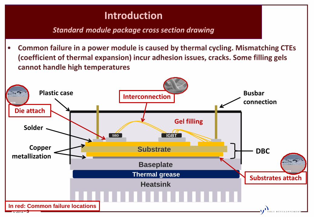
Introduction Standard module package cross section drawing
Heatsink
Thermal grease
Substrate
SBD IGBT
Baseplate
DBC
Busbar connection
Solder
Copper metallization
Plastic case
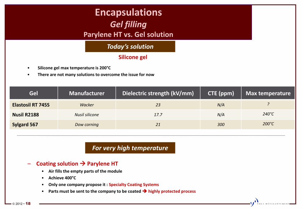
• Common failure in a power module is caused by thermal cycling. Mismatching CTEs (coefficient of thermal expansion) incur adhesion issues, cracks. Some filling gels cannot handle high temperatures
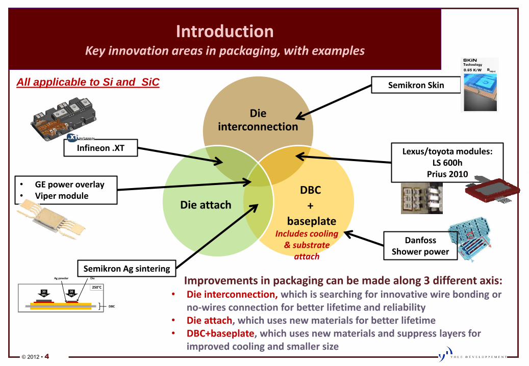
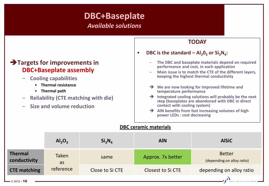
Introduction Key innovation areas in packaging, with examples
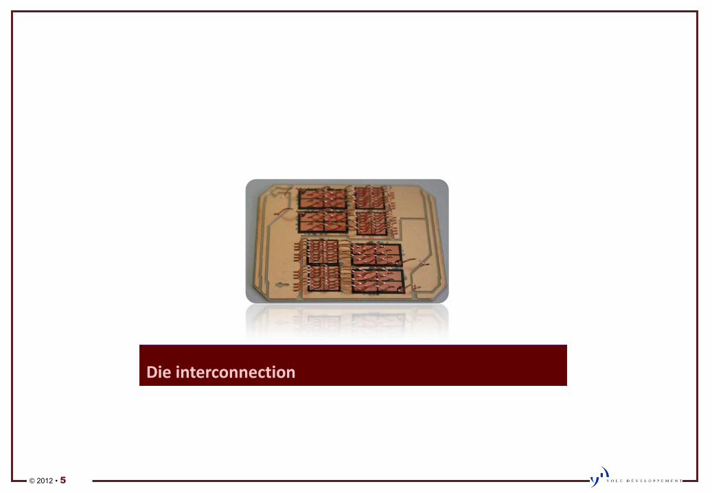
Die interconnection
DBC
+
baseplate
Die attach
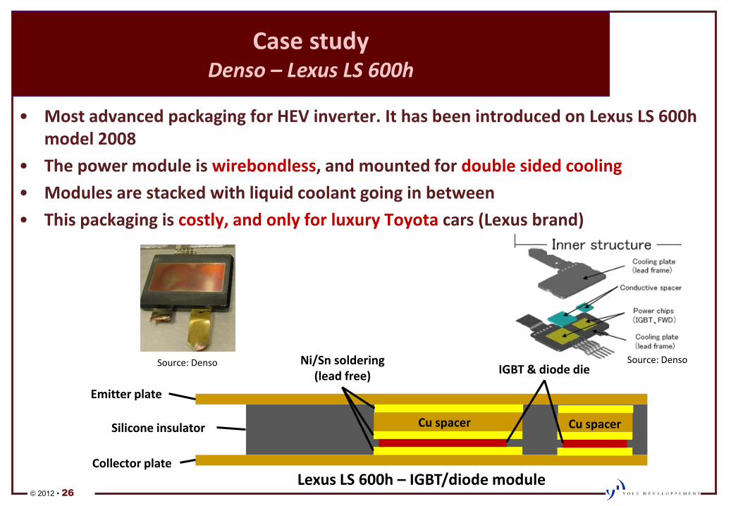
Infineon .XT Lexus/toyota modules: LS 600h
Prius 2010
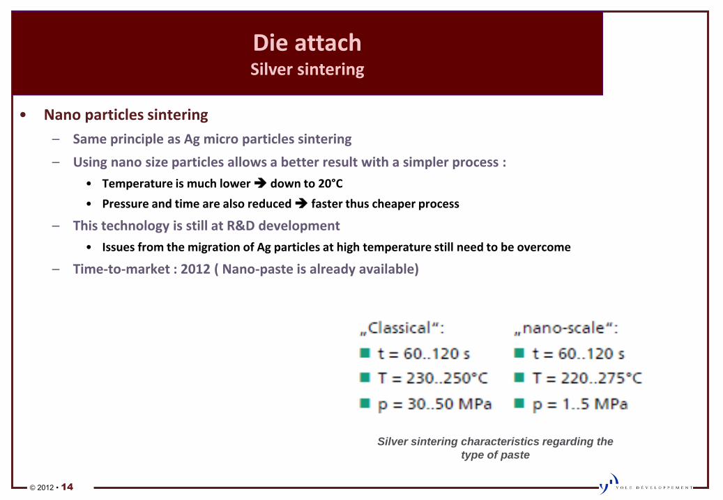
Semikron Ag sintering
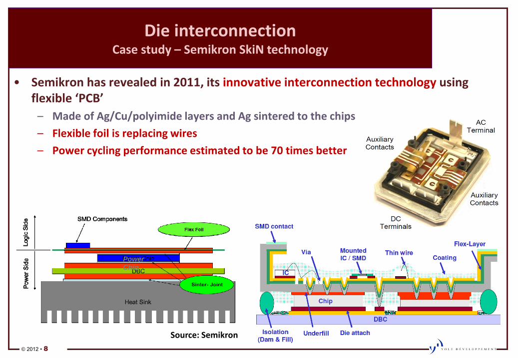
Semikron Skin
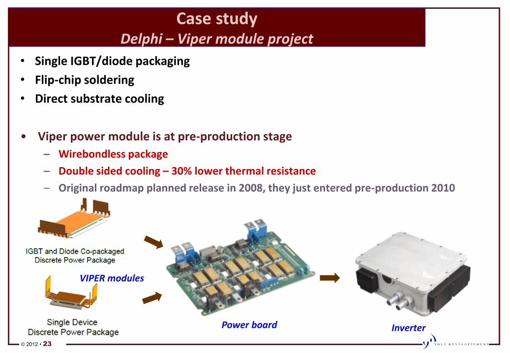
• GE power overlay • Viper module
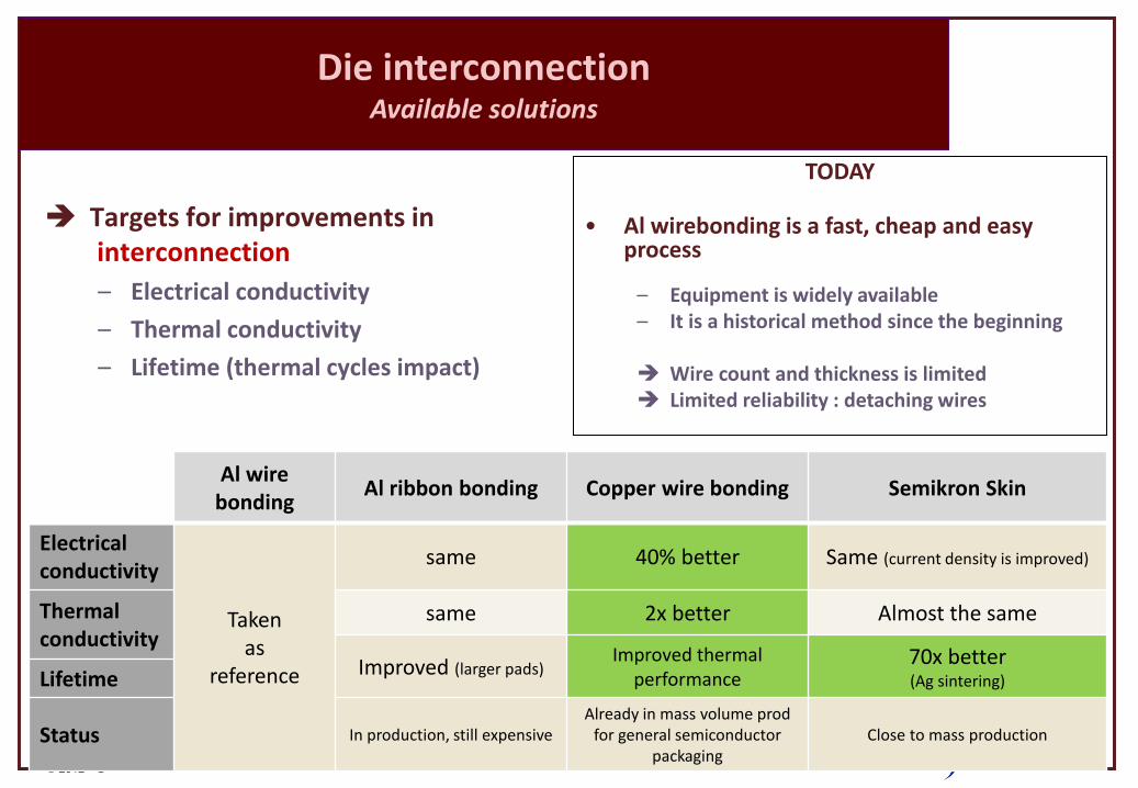
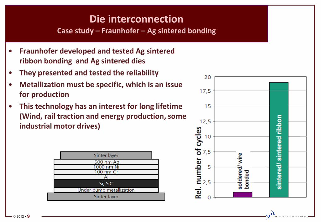
Improvements in packaging can be made along 3 different axis: • Die interconnection, which is searching for innovative wire bonding or
no-wires connection for better lifetime and reliability • Die attach, which uses new materials for better lifetime • DBC+baseplate, which uses new materials and suppress layers for
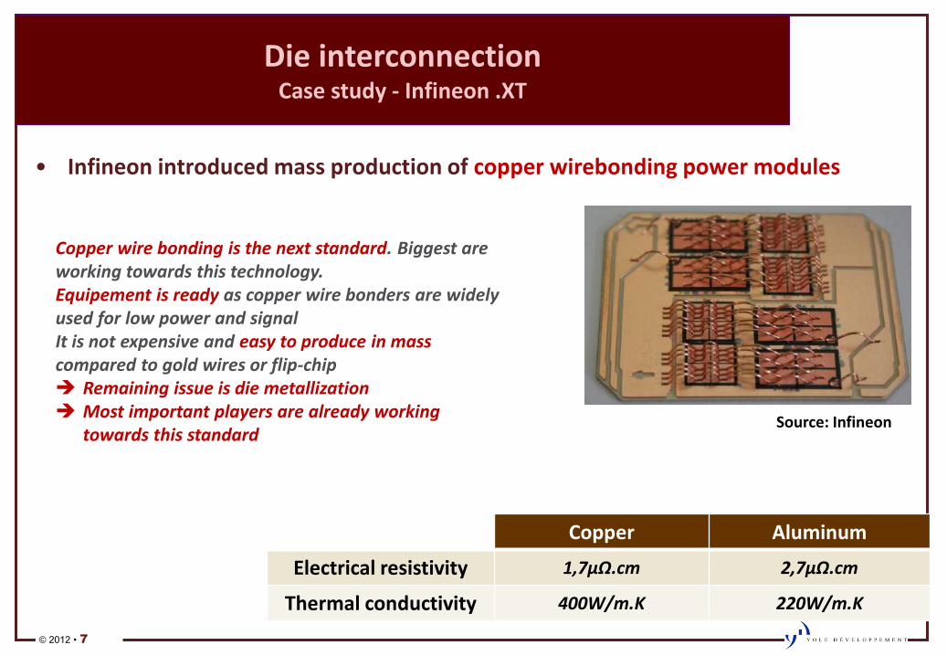
• Infineon introduced mass production of copper wirebonding power modules
Copper Aluminum
Electrical resistivity 1,7µΩ.cm 2,7µΩ.cm
Thermal conductivity 400W/m.K 220W/m.K
Source: Infineon
Copper wire bonding is the next standard. Biggest are working towards this technology. Equipement is ready as copper wire bonders are widely used for low power and signal It is not expensive and easy to produce in mass compared to gold wires or flip-chip Remaining issue is die metallization Most important players are already working
Die interconnection Case study – Fraunhofer – Ag sintered bonding
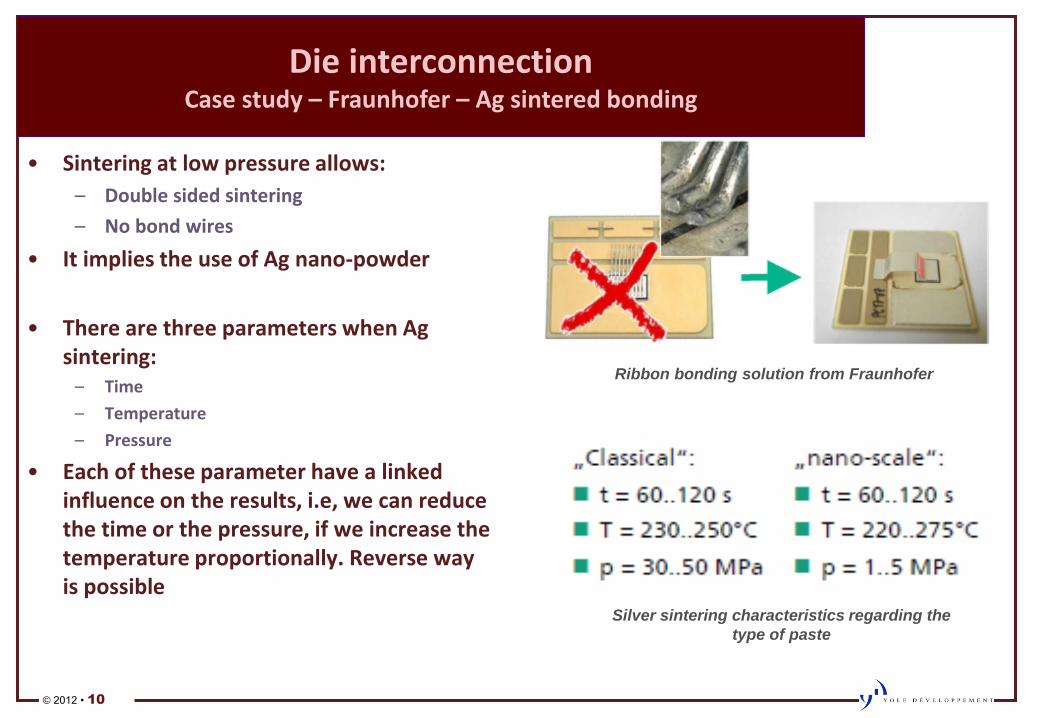
• Sintering at low pressure allows:
– Double sided sintering
– No bond wires
• It implies the use of Ag nano-powder
• There are three parameters when Ag sintering: – Time
– Temperature
– Pressure
• Each of these parameter have a linked influence on the results, i.e, we can reduce the time or the pressure, if we increase the temperature proportionally. Reverse way is possible
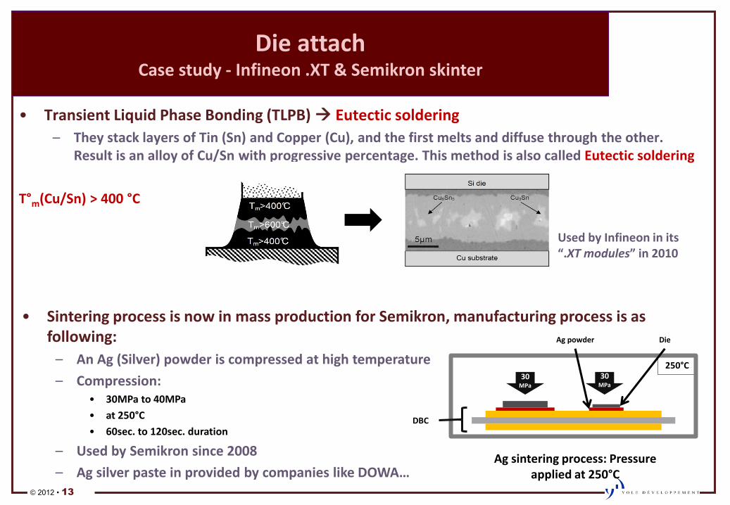
– They stack layers of Tin (Sn) and Copper (Cu), and the first melts and diffuse through the other. Result is an alloy of Cu/Sn with progressive percentage. This method is also called Eutectic soldering
T°m(Cu/Sn) > 400 °C
Die attach Case study - Infineon .XT & Semikron skinter
Used by Infineon in its “.XT modules” in 2010
• Sintering process is now in mass production for Semikron, manufacturing process is as following:
– An Ag (Silver) powder is compressed at high temperature
– Compression: • 30MPa to 40MPa
• at 250°C
• 60sec. to 120sec. duration
– Used by Semikron since 2008
– Ag silver paste in provided by companies like DOWA…
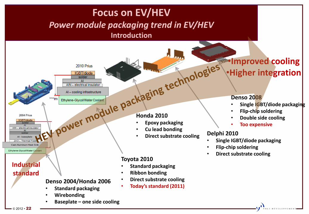
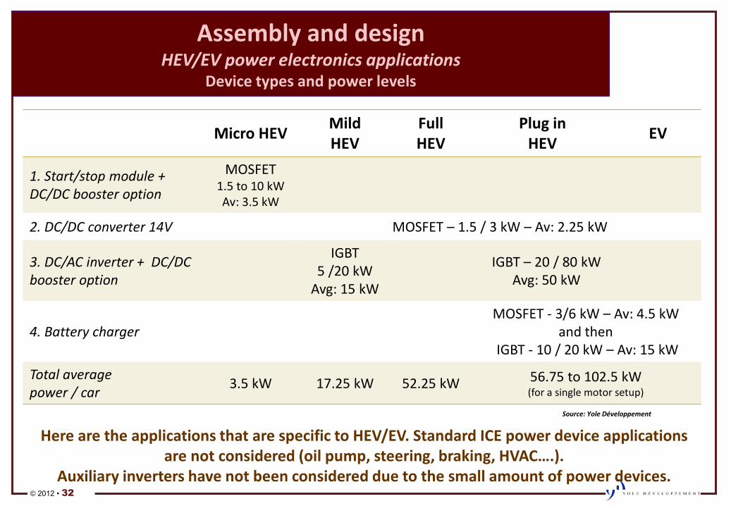
Focus on EV/HEV Power module packaging trend in EV/HEV
Introduction
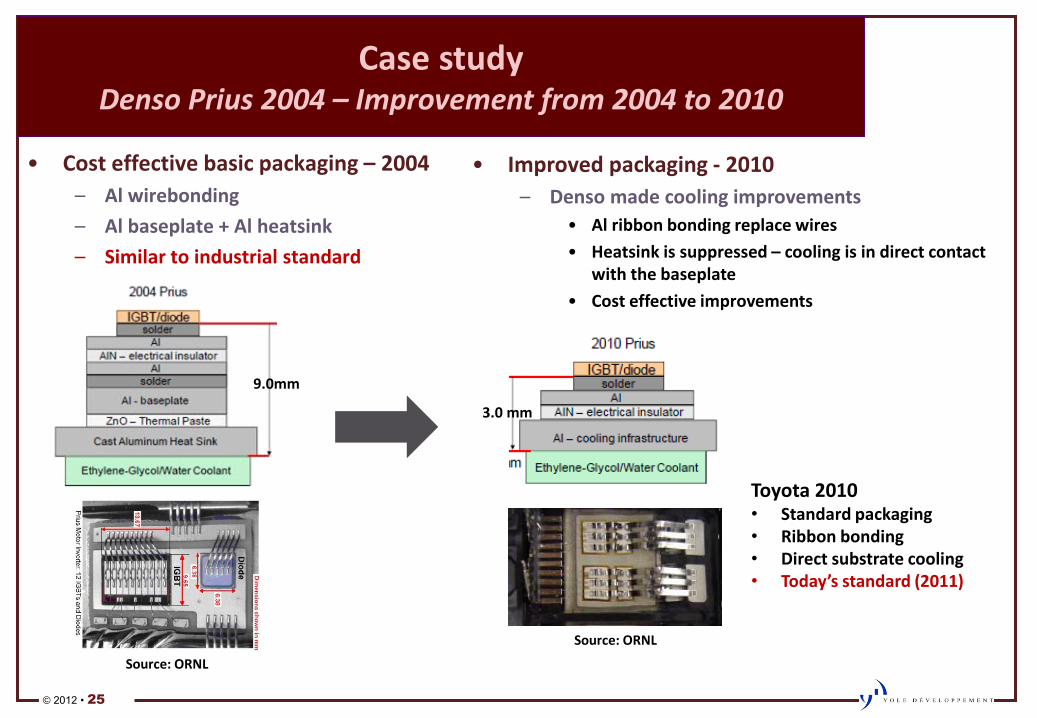
3.0 mm
9.0mm
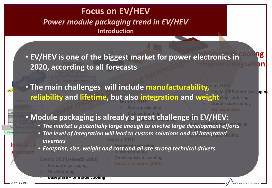
Denso 2004/Honda 2006 • Standard packaging • Wirebonding • Baseplate – one side cooling
Toyota 2010 • Standard packaging • Ribbon bonding • Direct substrate cooling • Today’s standard (2011)
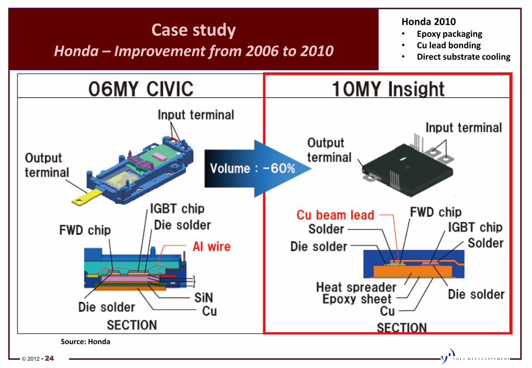
Honda 2010 • Epoxy packaging • Cu lead bonding • Direct substrate cooling Delphi 2010
• Single IGBT/diode packaging • Flip-chip soldering • Direct substrate cooling
Denso 2008 • Single IGBT/diode packaging • Flip-chip soldering • Double side cooling • Too expensive
•Improved cooling •Higher integration
Industrial standard
• EV/HEV is one of the biggest market for power electronics in 2020, according to all forecasts
• The main challenges will include manufacturability, reliability and lifetime, but also integration and weight
• Module packaging is already a great challenge in EV/HEV: • The market is potentially large enough to involve large development efforts • The level of integration will lead to custom solutions and all integrated
inverters • Footprint, size, weight and cost and all are strong technical drivers
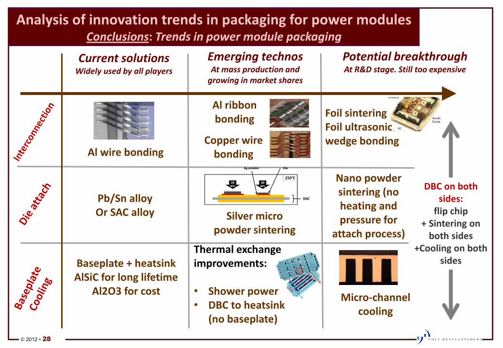
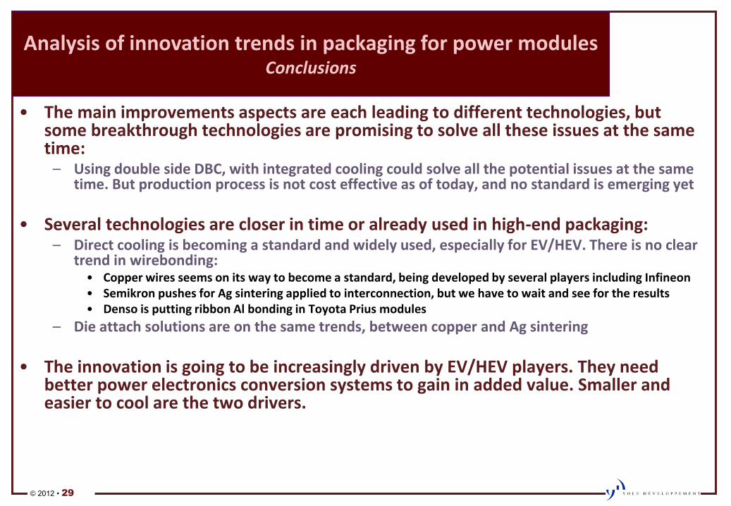
Analysis of innovation trends in packaging for power modules Conclusions
• The main improvements aspects are each leading to different technologies, but some breakthrough technologies are promising to solve all these issues at the same time: – Using double side DBC, with integrated cooling could solve all the potential issues at the same
time. But production process is not cost effective as of today, and no standard is emerging yet
• Several technologies are closer in time or already used in high-end packaging: – Direct cooling is becoming a standard and widely used, especially for EV/HEV. There is no clear
trend in wirebonding: • Copper wires seems on its way to become a standard, being developed by several players including Infineon • Semikron pushes for Ag sintering applied to interconnection, but we have to wait and see for the results • Denso is putting ribbon Al bonding in Toyota Prius modules
– Die attach solutions are on the same trends, between copper and Ag sintering
• The innovation is going to be increasingly driven by EV/HEV players. They need better power electronics conversion systems to gain in added value. Smaller and easier to cool are the two drivers.
3.5 kW 17.25 kW 52.25 kW 56.75 to 102.5 kW (for a single motor setup)
Here are the applications that are specific to HEV/EV. Standard ICE power device applications are not considered (oil pump, steering, braking, HVAC….).
Auxiliary inverters have not been considered due to the small amount of power devices.