NOTICE: The author has granted a non-exclusive license allowing Library and Archives Canada to reproduce, publish, archive, preserve, conserve, communicate to the public by telecommunication or on the Internet, loan, distribute and sell theses worldwide, for commercial or non-commercial purposes, in microform, paper, electronic and/or any other formats. .
AVIS: L’auteur a accordé une licence non exclusive permettant à la Bibliothèque et Archives Canada de reproduire, publier, archiver, sauvegarder, conserver, transmettre au public par télécommunication ou par l’Internet, prêter, distribuer et vendre des thèses partout dans le monde, à des fins commerciales ou autres, sur support microforme, papier, électronique et/ou autres formats.
The author retains copyright ownership and moral rights in this thesis. Neither the thesis nor substantial extracts from it may be printed or otherwise reproduced without the author’s permission.
L’auteur conserve la propriété du droit d’auteur et des droits moraux qui protège cette thèse. Ni la thèse ni des extraits substantiels de celle-ci ne doivent être imprimés ou autrement reproduits sans son autorisation.
In compliance with the Canadian Privacy Act some supporting forms may have been removed from this thesis. While these forms may be included in the document page count, their removal does not represent any loss of content from the thesis.
Conformément à la loi canadienne sur la protection de la vie privée, quelques formulaires secondaires ont été enlevés de cette thèse. Bien que ces formulaires aient inclus dans la pagination, il n’y aura aucun contenu manquant.
i
ABSTRACT
The transmission line based analytical solutions have simplified engineering of complex
microwave circuits like electromagnetic bandgap structures (EBGs). In this thesis, planar
EBG structures are studied by derivation of lumped element and transmission line
equivalent circuits followed by utilizing analytical formulations. Based on this approach,
a code is developed that predicts the dispersion characteristics of these periodic structures
in a matter of few seconds. Planar EBG structures containing meander sections are
investigated and a method for development of an equivalent circuit for the meander line
portion is presented. The analysis of the studied EBG structures begins from a simple 1D
geometry and is extended to more complex 2D geometries. The analytical simulation
results are evaluated against full-wave simulations. Inclusion of the meander sections
reduces the beginning of the bandgap to below 1GHz resulting in a more attractive
structure for low frequency omni-directional filtering.
ii
Abrégé
Les solutions analytiques basées sur des lignes de transmission ont simplifié l'ingénierie
de circuits micro-ondes complexes, tel que les EBG. La présente thèse étudie les
structures coplanaires EBG à partir d'éléments discrets et de modèles de lignes de
transmission, auxquels sont ensuite appliquées des formules analytiques. Grâce à cette
approche, un logiciel a été développé permettant de prédire les caractéristiques de
dispersion de ces structures périodiques en quelques secondes seulement. Les structures
coplanaires EBG contenant des sections courbes sont étudiées et un modèle de circuit
équivalent à la portion courbe est proposé. L'analyse des structures EBG commence par
une simple géométrie 1D, puis est étendue à des géométries 2D plus complexes. Le
résultat des simulations analytiques est évalué par rapport au résultat des simulations
analogues. Lorsque les sections courbes sont incluses, le début de la bande interdite est
porté en deçà de 1GHz, rendant la structure plus intéressante pour le filtrage basse
fréquence omni- directionnel.
iii
ACKNOWLEDGEMENTS
It is difficult not to overstate my gratitude to my supervisor, Prof. Ramesh Abhari. With
her enthusiasm, inspiration and great efforts to explain things as lucidly as possible, she
made my learning experience an absolute pleasure. Throughout the duration of my thesis
work, she provided encouragement, sound advice, good teaching and most importantly,
her invaluable time. It would be an understatement if I said that I would have been lost
without her guidance and able support.
I am thankful to my student colleagues, especially Kasra Payandehjoo, for sharing their
wealth of knowledge with me and always being there to help me out.
I would also like to thank Ashwan Singh and Yogini Nath for their immense help and
support. I would like to thank Madhusudanan Srinivasaraghavan and François Leduc-
Primeau for providing invaluable inputs during the thesis writeup.
Lastly, and most importantly, I wish to thank my parents, Mrs. Rajeshwari
Venkateswaran and Mr. P.N. Venkateswaran. No amount of words can express the
unconditional love and support I have received from them. To them I dedicate this thesis.
Figure 2.7: Lumped component model of a three conductor MTL segment [27] ............. 19
Figure 3.1: Top view of unit cells of various types of EBG structures ............................. 23
Figure 3.2: One dimensional representation of a periodic structure ................................. 26
Figure 3.3: An infinite x infinite dipole array with inter-element spacings
of xD and zD , and element length of l2 [50]. .................................................. 28
Figure 3.4: Array mutual impedance 1,2Z between an array with element orientation ( )1p and an external element with orientation ( )2p is obtained from the
Analysis of Planar EBG Structures Using Transmission Line Models 1
CHAPTER 1 Introduction
Advances in fabrication technology have enabled realization of many complicated
microwave circuits using low cost printed circuit board technologies. Electromagnetic
bandgap structures (EBGs) [1]-[3], metamaterials [4], [5] and substrate integrated
waveguides (SIWs) [6], [7] are examples of such advanced structures. EBG structures are
used in designing low profile antennas, microwave filtering and noise suppression in
power delivery networks [3], [8]-[10].
Power/ground noise is an increasing problem in modern systems due to the ever rising
clock frequencies and decreasing rise and fall times associated with the newer
generations of electronic devices. EBG structures have been employed as filters for
suppression of noise in power distribution networks (PDNs). This is achieved by
replacing one of the power/ground planes by an EBG surface. The stopband induced by
the EBG layer suppresses the noise in all planar directions within the PDN. The EBG
layer is either a Textured (via based) or a Uniplanar (without vias) geometry. Figure 1.1
shows two parallel plate PDNs containing these two types of EBG structures. This thesis
focuses on the analysis of Uniplanar or planar EBG structures and in particular the
structures that can be modeled using lumped component and two-conductor transmission
line circuits. Determination of the stopbands and the degree of isolation obtained in the
forbidden bands of EBG structures in filtering and noise suppression applications are the
two most important measures of their efficiency. These characteristics can be ascertained
from the dispersion diagram and scattering parameter (s-parameter) plots.
Over the past few years, different methodologies have been employed to generate the
dispersion and insertion loss plots and predict the modal characteristics of these
geometries. These methods include full wave numerical analysis and analytical solutions.
This thesis focuses on the analysis of planar EBG structures using transmission line
modeling and analytical solutions.
Analysis of Planar EBG Structures Using Transmission Line Models 2
1.1 Motivations and Objectives
As stated earlier, in order to predict the frequency selective behaviour of the EBG
structures, the dispersion characteristics and the s-parameters should be extracted. The
dispersion characteristic is the plot of propagation constant of every mode versus
frequency, commonly known as β−k diagram in waveguides. To obtain such plots,
eigenvalues of the electromagnetic problem should be found. The most commonly used
procedure to obtain these attributes is by utilizing commercial electromagnetic (EM) field
solvers. These tools are very accurate in predicting the EBG characteristics, but they
often require a lot of time to converge on the eigenvalues especially when a large number
of modes are investigated. Hence, any modification to the layout for the purpose of
design optimization results in hours of simulation time.
Figure 1.1: (Left) Textured and (Right) planar EBG structures sandwiched between
power planes for the suppression of noise in PCB designs
Two most commonly used EM solvers are Ansoft’s High Frequency Structure Simulator
(HFSS) and Agilent’s Advanced Design System (ADS). These tools are also used in the
investigation of the studied structures. In this thesis, driven port simulations in HFSS and
ADS Momentum are utilized for generating the s-parameters. Of the two solvers
Eigenmode solution is only available in HFSS and is used for generating the dispersion
diagrams. HFSS is a finite element method (FEM) based solver whereas ADS
Momentum is a Method of Moments (MoM) solver. FEM solvers divide the domain into
finite elements (triangles for 2D elements and tetrahedra for 3D elements). HFSS is an
efficient tool for the extraction of modal information. It can be used for simulation of
Analysis of Planar EBG Structures Using Transmission Line Models 3
antennas and includes definition of closed and open boundaries as well as perfectly
matched layers (PML). ADS Momentum is a planar analysis tool which can be broadly
used for the analysis of open and shielded 2.5D structures. The MoM also involves the
subdivision of the domain into a mesh. Once it is achieved, the MoM code solves for the
current on each small rectangular or triangular patch. Green’s function is used to fill the
moment matrix. Scattering parameters and radiation patterns are examples of output data
generated by ADS Momentum analysis. Both HFSS and ADS give extremely accurate
scattering parameter results but are expensive and time consuming. EBG structures have
become very popular in microwave engineering and there is a need for an inexpensive
way to analyze them. The goal of this thesis is to utilize an analytical method by which
the frequency selective characteristics of EBG structures could be predicted with an
acceptable degree of accuracy in a matter of few seconds, when compared to the
simulation time required by EM solvers.
1.2 Methodology
The primary objective of this thesis is to develop an alternative approach to predict the
dispersion and suppression characteristics of planar EBG structures in a cost effective
way. This is achieved by employing the transmission line modeling (TLM) method to
represent EBG structures. As stated earlier, Eigenmode analysis of EBG structures using
commercial EM solvers is expensive and time consuming. Moreover, the size of the mesh
associated with such structures is limited by the memory availability of the machine.
Hence, the only way around such a problem is a reduction in the mesh size, which
compromises the accuracy of the network and modal analysis. The method in this thesis
mainly relies on the derivation of simplified models and obtaining Kirchhoff’s Voltage
Law (KVL) and Kirchhoff’s Current Law (KCL) and multi-port network solutions. Since
the recently developed EBG structures are based on printed circuit geometries,
transmission line modeling (TLM) plays a significant role in their analytical investigation
[5], [11], [12].The equivalent circuit of an EBG structure can be composed of two or
multi-conductor transmission line segments with some lumped loading components to
represent the periodic discontinuity. Voltage and current variables, which could be
Analysis of Planar EBG Structures Using Transmission Line Models 4
vectors in the case of multi-conductor structures, are used to derive the representative
network parameters.
In order to find the eigenvalues of the system, Floquet’s theorem is applied to voltage and
current variables at the two ends of the unit cell of the EBG structure [13]. Solving the
resultant matrix equation yields the dispersion (or characteristic) equation of the EM
problem. The representative transfer matrix of the unit cell can be utilized to obtain
insertion loss signature of the structure without including the effect of excitation ports
and only by considering the number of cells between the two ports. A summary of the
steps involved in each of the processes to obtain the desired output data is shown in
Figure 1.2 . This diagram also serves as the basis for development of a TLM-code in
MATLAB.
In this thesis, in order to demonstrate the capability of the TLM based analysis, few
planar EBG geometries are analyzed. The results generated by the TLM-based code are
compared with those obtained from full-wave analysis. Using this analytical
methodology, the design of the EBG structures can be improved to achieve low
frequency stopbands below 1GHz.
1.3 Thesis organization
After the brief introduction provided in this chapter, Chapter 2 presents a review of
transmission line fundamentals, Chapter 3 surveys the history, fundamentals and
applications of EBG structures. Chapter 4 discusses the methodology for analysis of EBG
structures using transmission line modeling and provides examples of analysis of planar
EBG structures. Chapter 5 describes an analytical technique to obtain the equivalent
inductance of a meander line. Chapter 6 presents the analysis of a few planar EBG
structures containing meander line sections. Dispersion diagrams are generated to study
the modal characteristics of the geometries reviewed in Chapters 4 and 6. As well s-
parameter plots are obtained to provide information about the isolation achieved in the
investigated EBG geometries. In chapter 7, closing remarks and discussions about the
scope of future work are presented.
Analysis of Planar EBG Structures Using Transmission Line Models 5
β−k ( )α
Figure 1.2: Analysis procedure using transmission line modeling method
Analysis of Planar EBG Structures Using Transmission Line Models 6
CHAPTER 2 Review of Transmission Lines
This chapter reviews the analysis of various types of transmission lines that are
commonly used in electronic systems and discusses the differences between them. The
major part of the chapter deals with the derivation of the Telegraphers’ equations for two
conductor and multiconductor transmission line networks and describes the various
circuit parameters involved in the analysis.
2.1 Transmission Line Circuits
When analyzing transmission line circuits, generally their lumped element model or
distributed element model is referred. Maxwell’s equations are applicable to all types of
electromagnetic behaviour at all frequencies. When the electrical length of the circuit is
smaller than the operating wavelength of the circuit, static field equations apply, and
lumped components are used to represent the electrically small section of a transmission
line. In such cases, the circuit components can be considered as frequency independent
parameters. The lumped component model is also utilized when modeling transmission
line discontinuities with parasitic components [14]. At higher frequencies, such as those
in the microwave region (defined between 300 MHz to 30 GHz [13]), the electrical
length of the circuit becomes relatively large due to which the time delay factor becomes
prominent and wave equations should be used in the analysis of circuits. In this case, the
circuit is known as a distributed circuit. In such cases, a distributed element model is
preferred. The distributed model can be assumed to be composed of small lumped
element sections. For circuits operating at microwave and millimetre wave frequencies
and even in the analysis of micro-scale circuits such as ICs, distributed models are often
used.
Transmission line circuits have been utilized as signal guiding structures for over 50
years [15]. Some of the most popular transmission lines that are used in printed circuits
include striplines, microstrip lines, coplanar waveguides and twinstrips, slotlines and
finlines [16]. Striplines most commonly employ homogenous dielectrics, thus supporting
a dominant transverse electromagnetic (TEM) propagating mode. Their major
Analysis of Planar EBG Structures Using Transmission Line Models 7
applications include the design of microwave filters [17], hybrids [18], directional
couplers [19] and stepped impedance transformers [20]. Microstrip lines are preferred in
low cost circuit design because of the convenience they provide in the mounting of the
transistors or lumped components. The drawback associated with microstrip lines is the
difficulty in accessing the ground plane that requires punching through the substrate. In
addition to this, the substrate must be very thin in order to avoid higher order mode
propagation at higher frequencies [16]. This would result in a very delicate framework.
This was considered in the development of other types of transmission lines such as
coplanar waveguides and twinstrip lines. These transmission lines were realized by
moving the ground plane to the same side of the substrate as the signal land. The signal
line could either be placed symmetrically between the two ground plane lands (coplanar
waveguide) or adjacent to a single ground land (twinstrip). Slotlines have been used in
conjunction with microstrip lines to design filters [21] and directional couplers [22].
Finlines (also referred to as E-planes [16], [23]) have been used to create filters [24],
detectors [23] and mixers [25], [26]. Figure 2.1 shows the various commonly used
microwave planar transmission lines.
Microstrip lines, owing to the non homogenous nature of the dielectric medium, support
hybrid TE and TM modes. At lower frequencies, microstrips appear to have a guided
wavelength and characteristic impedance very similar to that of a TEM line. As the
frequency increases, this mode deviates from the TEM behaviour and hence such a mode
is conceptually referred to as a quasi-TEM mode.
Another type of transmission line is a parallel plate two conductor system which, as the
name suggests, consists of parallel conductor plates as shown in Figure 2.2. The power
distribution network (PDN) in various printed circuit systems like PCBs, ICs, is used to
provide biasing current to the circuit components constituting a system. In addition to this
the power/ground planes also act as efficient shields.
In addition to routing signals between two or more locations, transmission lines are the
basic structures used in creating filters, couplers, resonators and circuit components.
Hence, analysis of a two conductor transmission line provides invaluable insight into the
Analysis of Planar EBG Structures Using Transmission Line Models 8
propagation characteristics of electromagnetic waves in such structures. Derivations of
voltage and current wave equations are discussed in the following section.
Figure 2.1: Planar microwave transmission lines
( )tz,E x
( )tz,H y
Figure 2.2: Parallel plate two conductor system
2.2 Analysis of Two Conductor Transmission Lines
As stated earlier, transmission line analysis is employed when the length of the
transmission line is a comparable fraction of the signal wavelength. Circuit theory deals
with only lumped component parameters whereas transmission line theory deals with
Analysis of Planar EBG Structures Using Transmission Line Models 9
distributed component parameters. If we consider a small segment of a transmission line
of length z∆ shown in Figure 2.3, then the lumped element circuit model of that section
of transmission line can be represented as shown in Figure 2.4 [13]. The lumped
component model consists of series resistance, series inductance, shunt capacitance and
shunt conductance, all of which have been normalized per unit length of the transmission
line.
Figure 2.3: Section of a transmission line [13]
Figure 2.4: Lumped component model of the section of transmission line [13]
where =R Per unit length series resistance in m/Ω
=L Per unit length series inductance in mH /
=G Per unit length shunt conductance in mS /
=C Per unit length shunt capacitance in mF /
Analysis of Planar EBG Structures Using Transmission Line Models 10
Applying Kirchhoff’s Voltage Law to the circuit shown in Figure 2.4, we obtain,
( ) ( ) ( ) ( ) 0,,
,, =∆+−∂
∂∆−∆− tzzv
ttzi
zLtzziRtzv (2.1)
Similarly, applying Kirchhoff’s Current Law to the circuit shown in Figure 2.4, we
obtain,
( ) ( ) ( ) ( ) 0,,
,, =∆+−∂∆+∂
∆−∆+∆− tzzit
tzzvzCtzzzvGtzi (2.2)
Dividing (2.1) and (2.2) by z∆ and applying0
lim→∆z
, we obtain the following set of
differential equations,
( ) ( ) ( )
ztzi
LtzRiztzv
∂∂
−−=∂
∂ ,,
, (2.3)
( ) ( ) ( )
ztzv
CtzGvztzi
∂∂
−−=∂
∂ ,,
, (2.4)
(2.3) and (2.4) are known as Telegraphers’ equations.
The steady state equations for (2.3) and (2.4) are:
( ) ( )zILjRzzV
)( ω+−=∂
∂ (2.5)
( ) ( )zVCjGzzI
)( ω+−=∂∂
(2.6)
Partially differentiating (2.5) and (2.6) with respect to z
( ) ( )
zzI
LjRzzV
∂∂
+−=∂
∂)(2
2
ω (2.7)
( ) ( )
zzV
CjGzzI
∂∂
+−=∂∂
)(2
2
ω (2.8)
Substituting (2.5) and (2.6) in (2.8) and (2.7) respectively
( ) ( )zVCjGLjRzzV
))((2
2
ωω ++=∂
∂ (2.9)
( ) ( )zILjRCjGzzI
))((2
2
ωω ++=∂∂
(2.10)
Analysis of Planar EBG Structures Using Transmission Line Models 11
Rearranging (2.9) and (2.10), we obtain the voltage and current wave equations as
follows:
( ) ( ) 022
2
=−∂
∂zV
zzV
γ (2.11)
( ) ( ) 022
2
=−∂∂
zIzzI
γ (2.12)
where βαωωγ jCjGLjR +=++= ))(( (2.13)
is the complex propagation constant of the transmission line and is a frequency dependent
parameter. The propagation constant is a measure of the change in the amplitude and
phase of a wave between the points of origin or reference, and a point at a distance z as
it travels along the transmission line.
The propagation constant consists of two discernible parts: (a) A real part ‘α ’ known as
the attenuation constant which is a measure of the attenuation that a wave suffers per
metre travel along the transmission line, and (b) an imaginary part ‘ β ’ known as the
phase constant. β , along with the characteristic impedance 0Z (refer to Equation (2.16)),
is one of the two most important descriptive parameters of a transmission line and is a
measure of the change in phase that a wave suffers per metre travel along the
transmission line.
The solution to the set of differential equations (2.11) and (2.12) is given by
( ) zz eVeVzV γγ +−−+ += 00 (2.14)
( ) zz eIeIzI γγ +−−+ += 00 (2.15)
where +0V and +
0I are the amplitudes of the voltage and current of the incident wave, and
similarly, −0V and −
0I are amplitudes of the voltage and current of the reflected wave.
The characteristic impedance of a transmission line is defined by
CjGLjR
I
V
I
VZ
ωω
++
===−
−
+
+
0
0
0
00 (2.16)
Analysis of Planar EBG Structures Using Transmission Line Models 12
Whenever a transmission line is terminated in an arbitrary load, 0ZZ L ≠ , an important
parameter, known as the reflection coefficient, comes into existence. The refection
coefficient is given by
0
0
ZZZZ
L
L
+−
=Γ (2.17)
The return loss (RL) of a transmission line is a measure of the amount of power delivered
from the source to the load and is provided by the equation
dBlog20RL Γ−= (2.18)
A matched load (which implies no part of the incident power is reflected) has RL of ∞
dB whereas total reflection (which implies all the incident power is reflected) has a RL of
0 dB.
2.3 Analysis of Multi-conductor Transmission Lines (MTLs)
Having investigated a two conductor transmission line in the previous section, we now
investigate a multiconductor transmission line segment [27] as shown in Figure 2.5. The
system is composed of n'' conductors and the conductor numbered ‘0’, which provides
the return path for all the other conductors in the system, is defined as the reference
conductor.
For the Voltage equation:
According to Faraday’s law
∫ ∫ ⋅−=⋅c s
sdHdtd
ldErrrr
µ (2.19)
When we apply Faraday’s law along the contours ,,, cdbcab and da which enclose the
surface is and move in a clockwise direction, we obtain
( )∫∫∫∫∫ −⋅−=⋅+⋅+⋅+⋅is
nt
a
dl
d
ct
c
bl
b
at sdaH
dtd
ldEldEldEldErrrrrrrrrr
ˆµ (2.20)
where tEr
and tHr
represent the transverse electric and magnetic fields (with the subscript
‘t’ representing the transverse direction) and lEr
represents the longitudinal electric field
(with the subscript ‘l’ representing the longitudinal direction). na is the surface unit
Analysis of Planar EBG Structures Using Transmission Line Models 13
vector na directed perpendicular to the surface is and is directed out of the plane. Since
na and the magnetic field associated with the surface is are in opposite directions, hence
the right hand side (RHS) term will become positive and hence (2.20) evolves to the
following,
z zz ∆+
lE
lE
tE tEna
tH
dsis
∑=
3
1kkI
),(1 tzI
),( tzIn
),(2 tzI
( )tzVi , ( )tzzVi ,∆+ic
Figure 2.5 Definition of contour for the derivation of first set of MTL equation [27]
( )∫∫∫∫∫ ⋅=⋅+⋅+⋅+⋅is
nt
a
dl
d
ct
c
bl
b
at sdaH
dtd
ldEldEldEldErrrrrrrrrr
ˆµ (2.21)
We consider a TEM mode of propagation and in accordance with such a mode, the
voltage relationships between the thi conductor and the reference conductor at the
beginning and at the end of the section are given by
( ) ( )∫ ⋅−=b
ati ldtzyxEtzV
rr,,,, (2.22)
( ) ( )∫ ⋅∆+−=∆+d
cti ldtzzyxEtzzV
rr,,,, (2.23)
Analysis of Planar EBG Structures Using Transmission Line Models 14
Since a TEM mode of propagation is possible only in perfect conductors, in order to
accommodate wave propagation in imperfect conductors in a quasi-TEM mode of
propagation, we include a per-unit-length conductor resistance, r mΩ .
For the purpose of simplification of our analysis, let us consider an MTL segment
consisting of three conductors and one reference conductor [27].
Voltage drops along the sections (assuming imperfect conductor):
Along bc = ∫ ⋅−c
bl ldE
rr (2.24)
Along da = ∫ ⋅−a
dl ldE
rr (2.25)
Or we can say that:
( )tzzIrldE ii
c
bl ,∆−=⋅− ∫
rr (2.26)
( )tzzIrldEa
dl ,00∆−=⋅− ∫
rr (2.27)
where 0& rri are the per unit conductor resistances of the thi and reference conductors,
and ( )tzI i , & ( ) ( )∑=
=3
10 ,,
kk tzItzI (k varies from 1 to 3 because we are analysing a
specific case of three conductors for an n-conductor multiconductor transmission line
system) are the currents on the thi and reference conductors.
According to Ampere’s law:
( ) ∫ ⋅=ic
ti ldHtzIrr
, (2.28)
where ic is a contour just off the surface of the thi conductor and enclosing the thi
conductor.
Substituting (2.22) to (2.28) in (2.20) we get:
( ) ( ) ( ) ( ) ( )∫∑ −⋅=∆++∆+∆+−=
isnti
kkiii sdaH
dtd
tzzVtzIzrtzzIrtzVrr
ˆ,,,,3
10 µ (2.29)
Rearranging the above equation
Analysis of Planar EBG Structures Using Transmission Line Models 15
( ) ( ) ( ) ( ) ( )∫∑ ⋅+
∆+∆−=−∆+
=is
ntk
kiiii sdaHdtd
tzIzrtzzIrtzVtzzVrr
ˆ,,,,3
10 µ (2.30)
Dividing the LHS and RHS by z∆
( ) ( ) ( ) ( ) ( )∫∑ ⋅
∆+
+−=
∆−∆+
=is
ntk
kiiii sdaH
dtd
ztzIrtzIr
ztzVtzzV rr
ˆ1,,
,, 3
10 µ (2.31)
Hence,
( ) ( ) ( ) ( ) ( ) ( )[ ]
( )∫ ⋅∆
+
++−−=∆
−∆+
isnt
iiii
sdaHdtd
z
tzItzItzIrtzIrz
tzVtzzV
rrˆ1
,,,,,,
3210
µ (2.32)
The total magnetic flux penetrating the surface is given by
∑∫=
=→∆
=⋅∆
−=3
10
ˆ1lim
n
jjij
sntzi IlsdaH
zi
rrµψ (2.33)
where ijl refers to the per-unit-inductance in mH
Applying 0
lim→∆z
in (2.32) and substituting (2.33) in it, we obtain
( ) ( ) ( ) ( ) ( )
( ) ( ) ( )ttzI
lttzI
lttzI
l
tzIrtzIrrtzIrztzV
iii
iii
∂∂
−∂
∂−
∂∂
−
+−−=∂
∂
,,,
,...,...,,
33
22
11
30010
(2.34)
Using matrix notation, (2.34) can be rewritten as [27]
( ) ( ) ( )
ttzI
LtzRIztzV
∂∂
−−=∂
∂ ,,
, (2.35)
where,
( )( )( )( )
=
tzV
tzV
tzV
tzV
,
,
,
,
3
2
1
(2.36)
( )( )( )( )
=
tzI
tzI
tzI
tzI
,
,
,
,
3
2
1
(2.37)
The per-unit-inductance matrix is given by
Analysis of Planar EBG Structures Using Transmission Line Models 16
=
333231
232221
131211
lll
lll
lll
L (2.38)
and the per-unit-resistance matrix is denoted by
+
+
+
=
3000
0200
0010
rrrr
rrrr
rrrr
R (2.39)
We can clearly observe that (2.35) is identical to the two conductor transmission line
equation (2.5) derived in the previous section.
For the current equation:
Referring to Figure 2.6, let us consider a surface s enclosing the thi conductor as shown.
It consists of two parts; the end areas represented by es and the enclosing section
represented by os . The continuity equation for the conservation of charge states
∫∫ ∂∂
−=⋅s
encQt
sdJˆ
ˆrr
(2.40)
where encQ is the charge enclosed by the surface.
Applying the continuity equation to over the end caps we have,
( ) ( )∫∫ −∆+=⋅es
ii tzItzzIsdJˆ
,,ˆrr
(2.41)
Similarly, application of the continuity equation over the side surface yields,
∫∫∫∫ ⋅=⋅oo s
ts
c sdEsdJˆˆ
ˆˆrrrr
σ (2.42)
where tc EJrr
σ= is the conduction current and (2.42) represents the transverse current
flowing between the conductors.
Again, for the purpose of simplification of our analysis, let us consider an MTL segment
consisting of three conductors and one reference conductor [27].
Analysis of Planar EBG Structures Using Transmission Line Models 17
z zz ∆+
ds),( tzI i na
tE
tE),( tzVi ),( tzzVi ∆+
os
es
µεσ ,,
),( tzzI i ∆+
Figure 2.6: Definition of contour for the derivation of second set of MTL equation [27]
We know that,
( ) ( ) ( )
( ) ( ) ( ) ( )∑
∫∫
=
→∆
+−−−=
−+−+−=⋅∆
3
1332211
33ˆ
22110
,,,,
ˆ1lim
0
kkikiii
iis
iiiitz
tzVgtzVgtzVgtzVg
VVgVVgVVgsdEz
rrσ
(2.43)
where ijg is the per-unit-conductance in mS
By Gauss’s law, the total charge enclosed by the surface encircling the conductor is given
by,
∫∫ ⋅=0ˆ
ˆs
tenc sdEQrr
ε (2.44)
The charge per unit length of line is obtained by [27],
Analysis of Planar EBG Structures Using Transmission Line Models 18
( ) ( ) ( )
( ) ( ) ( ) ( )∑
∫∫
=
→∆
+−−−=
+−+−+−=⋅∆
3
1332211
332211ˆ
0
,,,,
ˆ1lim
0
kkikiii
iiiiiiiiis
tz
tzVctzVctzVctzVc
VcVVcVVcVVcsdEz
rrε
(2.45)
where ijc is the per-unit-capacitance in mF
Substituting (2.41), (2.42) and (2.44) in equation (2.40), we get,
( ) ( ) ∫∫∫∫ ⋅−=⋅+−∆+00 ˆˆ
ˆˆ,,s
ts
tii sdEsdEtzItzzIrrrr
εσ (2.46)
Dividing both sides by z∆ we get,
( ) ( )
∫∫∫∫ ⋅∆
−=⋅∆
+∆
−∆+
00 ˆˆ
ˆˆ,,
st
st
ii sdEz
sdEzz
tzItzzI rrrr εσ (2.47)
Applying 0
lim→∆z
to (2.47) and substituting (2.43) and (2.45) yields,
( ) ( ) ( ) ( ) ( )
( ) ( ) ( ) ( )
−++
∂∂
+
−++=∂
∂
∑
∑
=
=
3
1332211
3
1332211
,,,,
,,,,,
kkikiii
kkikiii
i
tzVctzVctzVctzVct
tzVgtzVgtzVgtzVgztzI
(2.48)
( ) ( ) ( )tzV
tCtzGV
ztzI i ,,
,∂∂
−=∂
∂≈ (2.49)
where the per-unit-conductance matrix is represented as
++−−
−++−
−−++
=
3332313231
2323222121
1312131211
ggggg
ggggg
ggggg
G (2.50)
and the per-unit-capacitance matrix is represented as
++−−
−++−
−−++
=
3332313231
2323222121
1312131211
ccccc
ccccc
ccccc
C (2.51)
It can be observed that (2.49) resembles (2.6) derived in the previous section pertaining to
two conductor transmission lines. Figure 2.7 shows a lumped component model of a four
conductor MTL segment, one of which is a reference conductor.
Analysis of Planar EBG Structures Using Transmission Line Models 19
zr ∆3
zr ∆2
zr ∆1
zr ∆− 0
zl ∆33
zl ∆22
zl ∆11
zg ∆32
zg ∆33
zg ∆31zg ∆12
zg ∆11 zg ∆22
zc ∆32
zc ∆12 zc ∆31
zc ∆11 zc ∆22 zc ∆33
),(1 tzI
),(2 tzI
),(3 tzI
),(1 tzzI ∆+
),(2 tzzI ∆+
),(3 tzzI ∆+
∑=
∆+3
1
),(k
k tzzI∑=
3
1
),(k
k tzI
),(1 tzV
),(2 tzV
),(3 tzV
),(1 tzzV ∆+
),(2 tzzV ∆+zlij∆
Figure 2.7: Lumped component model of a three conductor MTL segment [27]
2.4 Conclusion
This chapter presented a brief discussion about the types and applications of transmission
lines.The fundamentals of transmission line networks discussed in this chapter are
essential in analytical studies of a transmission line circuit. In the subsequent chapters,
we will discuss equivalent models of various transmission line based geometries and
utilize analytical derivations to find the network parameters of the studied structures. The
important parameter that we intend to find in the analysis is the propagation constant, β ,
of the transmission line-based circuit.
Analysis of Planar EBG Structures Using Transmission Line Models 20
CHAPTER 3 Electromagnetic Bandgap
Structures
Electromagnetic bandgap (EBG) structures are periodic geometries constructed by
repetition of a unit cell or building block in one, two or three dimensions. Mostly they are
used to ideally eliminate propagation of electromagnetic waves within certain frequency
bands. Practically though, only partial elimination is possible. One dimensional (1D)
periodic structures, i.e. structures in which repetition of the unit cell occurs in one
dimension, are often utilized as microwave filters. Their properties have been studied in
[13], [25]-[28]. Two dimensional (2D) periodic structures, i.e. repetition exists along two
directions, are the most popular type of EBG structures. They have been utilized in the
design of antennas, microwave filters and even for suppression of power/ground or
simultaneous switching noise (SSN) in electronic circuits [29] and [30]. They have been
dealt with in numerous publications due to the ease of fabrication especially when
compared with 3D geometries. Three dimensional (3D) EBG structures, i.e. unit cell
repeats along all three spatial dimensions, have been studied in [31]. Note that the 1D
and 2D EBG structures may be 3D geometries as they are often developed on a dielectric
substrate and may include a conductor plane for grounding or shielding. The most
commonly used 2D EBG structures in microwave circuits contain conductor parts like an
array of metal protrusions or metal patches arranged in one or two dimensions.
Terminologies like High impedance surfaces (HIS) [28] or Frequency Selective Surfaces
(FSSs) are also used to refer to 2D EBG structures especially when they are used as
reflector planes and for the purpose of spatial wave filtering or eliminating surface waves
and currents.
This chapter provides a brief introduction about common 2D EBG structures, explains
their modal characteristics and elaborates on some important applications.
Analysis of Planar EBG Structures Using Transmission Line Models 21
3.1 Overview of EBG Geometries
EBG structures used in microwave and electronic engineering are mainly 2D periodic
structures. These 2D geometries can be broadly classified into two categories: Textured
(Mushroom or thumbtack) type and Uniplanar (or patterned) structures. Textured
surfaces consist of an array of bumps and waves travelling over such an undulating
surface, interact with these small bumps. The bumps basically behave as speed breakers
and hence there is a change in the velocity of the bound waves when they travel over
these bumps [28]. Due to the interference and change in velocity brought about by this
association, the textured surfaces prevent the propagation of surface bound waves and
this results in the production of a two directional bandgap [28]. Initial studies of this type
of structure involved obtaining a high impedance surface by using small bumps patterned
on a silver film [32], [33]. These bumpy structures were later developed into the
mushroom structures, also known as Sievenpiper’s structures [34]. These structures are
inductive at low frequencies and hence support TM waves and are capacitive at high
frequencies which enables them to support TE waves [28]. Within the forbidden gap
though, these structures suppress both TE and TM waves from propagating through the
structure.
Uniplanar or patterned EBG structures can be realized as a grid/meshed plane [35], a 2D
stepped impedance structure [36], interconnected slotted patches [37], metal patches
connected by meander lines [3], [38] or other parasitic sections. Some of the geometries
used for developing planar patterned and mushroom EBG structures have been shown in
Figure 3.1. Figure 3.1 (a) is the mushroom structure developed by Sievenpiper [28].
Figure 3.1 (c) is another uniplanar EBG used for suppression of ground/power noise [39].
Figure 3.1 (d) is also another one of Sivenpiper’s EBG structures [26], [27], while Figure
3.1 (e) shows the structure without the via. Note that in Figures 3.1(a) and 3.1(e), a
double sided substrate is used and the via stitches the patches on one side to the solid
conductor on the other side. Figure 3.1 (f) is an L-bridge loaded transmission line
structure [40]. Figure 3.1(g) is the stepped impedance structure and Figure 3.1 (h) is a
meander loaded transmission line structure [41]. A modified geometry used to obtain
Analysis of Planar EBG Structures Using Transmission Line Models 22
ultra wide bandgap, known as a super cell [3], is shown in Figure 3.1 (i). The super cell
was designed by combining two different geometries into a super cell structure. The
bandgap obtained due to the new structure is found to amalgamate the bandgaps arising
due to individual geometries, in addition to the bandgap arising from the combined
periodicity formed by the super cell topology. All of these geometries have shown
bandgap properties and provide various degrees of isolation characteristics.
In this thesis, only patterned EBG geometries have been analyzed. The stepped
impedance structure of Figure 3.1(g) and the structure of metal patches connected by
meander lines shown in Figure 3.1(h) serve as the basis for the EBG geometries studied
in this thesis.
The geometry of these EBG structures can be altered in order to obtain the bandgap in the
desired frequency region. In simplified cases an EBG structure can be approximated with
a surface impedance. This enables prediction of the bandgap using analytical approaches.
3.2 Electromagnetic Waves Supported by EBG structures
3.2.1 Review of Maxwell’s Equations
Maxwell’s equations hinge on the idea that light is an electromagnetic wave and they
provide one of the most effective and succinct ways to correlate the electric and magnetic
fields associated with the wave to their sources such as charge density and current
density. Although deceptively simple to look at, these equations epitomize a high level of
mathematical sophistication. Table 3.1 summarizes these equations.
Analysis of Planar EBG Structures Using Transmission Line Models 23
Figure 3.1: Top view of unit cells of various types of EBG structures
Table 3.1: The differential form of Maxwell’s equations [42]
Name of the Law Equation
Gauss’ s Law ρ=•∇ D
Gauss’s law for magnetism [43]* 0B =•∇
Faraday’s Law of Induction tB
E∂∂
−=×∇
Ampere’s loop law tD
JH∂∂
+=×∇
* Although the term is widely used, it is not a universal law. This law is also known as “Absence of free magnetic poles” [44]
Analysis of Planar EBG Structures Using Transmission Line Models 24
where E is the electric field intensity in Volt/meter.
D is the electric flux density in Newton/Volt-meter.
ρ is the total charge density in Coulomb/m3
B is the magnetic field density in Tesla
H is the magnetic field intensity in Ampere/meter
J is the total current density in Ampere/m2
and,
D1
Eε
= (3.1)
Here 0εεε r= (3.2)
rε is the relative permittivity of the medium, 0ε is the free space permittivity in
Farads/metre, the value of which equals 8.85x10⁻¹² m-3kg-1s4A2
Another important expression is the equation of continuity which relates the electric
charge density to the electric current density.
t∂
∂−=•∇
ρJ (3.3)
These are the basic equations which can be used individually, as well as in combination
to describe the electromagnetic interactions taking place. The wave equation, also known
as Helmholtz’s equation, can be obtained by combining Faraday’s law and Ampere’s
loop law and is given by,
0F-F1 2
0 =×∇×∇ qkp
(3.4)
where 000 εµω=k is known as the free space wave number, and, ),( rrp εµ= ,
),( rrq µε= for H)(E,F = .
(3.4) is the governing expression for electromagnetic wave propagation in any medium
including periodic structure.
In a source-free region, (3.4) becomes
Analysis of Planar EBG Structures Using Transmission Line Models 25
0HH
0EE22
22
=+∇
=+∇
k
k (3.5)
Where k is known as the wave number and is given by
( )mrad u
kω
µεω == (3.6)
3.2.2 Floquet’s Theorem
The fundamental expression underlying the analysis of periodic structures is known as
Floquet theorem which was proposed by Gaston Floquet in [45]. The theorem is pertinent
to quantum mechanics and an analysis dealing with time dependent Schroedinger
equation (TDSE) has been described in [46]. Floquet theorem has also been discussed in
detail in [47]. According to this theorem, if we have a periodic continuous function ( )xQ
with a minimum period of π such that
( ) ( )xQxQ =+π (3.7)
Then the second order first degree differential equation
( ) 0" =+ yxQy (3.8)
has two continuously differentiable solutions )(1 xy and )(2 xy .
If we take a closer look at (3.5) and (3.8), we observe the correlation between the various
parameters ( kQy ⇔⇔ ;H)E,( )
Consider a characteristic equation is given by,
( ) ( ) 01'212 =++− ρππρ yy (3.9)
The above equation has two Eigen values in πρ iae=1 and πρ iae−=2 respectively. Since
both Eigen values are different from each other, then (3.9) has two linearly independent
solutions,
( ) ( )xpexf iax11 = (3.10)
( ) ( )xpexf iax22
−= (3.11)
where ( )xp1 and ( )xp2 are periodic functions with period π .
Analysis of Planar EBG Structures Using Transmission Line Models 26
In solid state physics, Felix Bloch applied the theorem to periodic boundary conditions
and generalized it to three dimensions. This came to be known as Bloch’s theorem.
Bloch’s work dealing with quantum mechanical structure of electrons in crystal lattices
which are periodic geometries has been discussed in detail in [48], [49].
Hence in analysis of periodic structures in microwave engineering often the terminology
Bloch-Floquet Theorem is used. According to this theorem, there exists a correlation
between the fields at a point in an infinite periodic structure and the fields at a point
period a away and they are found to differ from each other by a propagation factor ae γ− ,
where γ is the propagation constant in the direction of propagation.
Based on this theorem, for the structure shown in Figure 3.2 depicting a one dimensional
periodic structure with a periodd , the voltage and current relationships are given by
dnn eVV γ−
+ =1 (3.12)
dnn eII γ−
+ =1 (3.13)
Figure 3.2: One dimensional representation of a periodic structure
The most important derivation from Floquet’s theorem is the possibility of expressing
fields in a periodic geometry by restricting the analysis to a unit cell of the periodic
structure. Once the field solution F at a particular point is determined, it is possible to
predict the field solutions at a period ma , away by the following relationship,
( ) ( )zyxemazyx ma ,,F,,F γ−=+ (3.14)
Analysis of Planar EBG Structures Using Transmission Line Models 27
In this thesis, the analysis and prediction of the modal characteristics of the studied EBG
structures has been performed by using the methodology mentioned above, which
involves application of Bloch-Floquet theorem to a unit cell of the EBG structure.
3.2.3 Forward, Backward and Evanescent Waves in a Periodic Array
In order to examine the various modes supported by EBG structures, a review of
propagating modes in a 2D infinite periodic structure from [50] is presented here. A 2D
array of dipoles in Figure 3.3 is considered. The array is infinitely periodic along x- and
z-directions with a period xD and zD , respectively. The array is excited by plane wave
propagating in the direction described by
zyx szsysxs ˆˆˆˆ ++= (3.15)
where zyx sss ,, are referred to as the direction cosines of the unit direction vector s of the
plane wave.
Since it is an infinite periodic array, the current in each element obeys Floquet’s theorem
and is given by,
zzmxxq sDjsDjqm eeII ββ −−= 0,0 (3.16)
where q and m refer to the column and row of an element, and
0,0I refers to the current in the reference element in the array.
In accordance with Ohm’s law, the voltage in the reference element is,
[ ] 0,00,00,0 IZZV L += (3.17)
where ∑ ∑∞
−∞=
∞
−∞=
−−=q m
sDjsDjqm
zzmxxq eeZZ ββ,0
0,0 (3.18)
is known as the scan impedance [50] and is defined as the array mutual impedance of the
reference element. It is composed of numerous elemental mutual impedances referred to
as qmZ ,0 . LZ is the load impedance on the reference element.
Analysis of Planar EBG Structures Using Transmission Line Models 28
Figure 3.3: An infinite x infinite dipole array with inter-element spacings of xD and zD ,
and element length of l2 [50].
When we consider an array element arbitrarily oriented along ( )1p with the reference
element of the array at ( )1R and an external element oriented along ( )2p and having a
reference element at ( )2R (illustrated in Figure 3.4), then the mutual array impedance,
based on (3.16) and (3.17) is given in [50] as,
( ) ( )( )
( ) ( ) ( ) ( )[ ]∑ ∑∞
−∞=⊥⊥
∞
−∞=
⋅−−
+=−=k
tt
n y
rRRj
zx
PPPPr
eDD
ZIV
Z 2||
1||
21ˆ
0
0,0
1,21,2
12
2
β
(3.19)
where
++±
+=
zzy
xx D
nszryD
ksxrλλ
ˆˆˆˆ for 0≠y (3.20)
22
1
+−
+−=
zz
xxy D
nsD
ksrλλ
(3.21)
( ) ( ) ( )1
||
11
||
ˆˆ PnpP ⊥⊥ ⋅= (3.22)
Analysis of Planar EBG Structures Using Transmission Line Models 29
( ) ( ) ( )tt PnpP 2
||
22
||
ˆˆ ⊥⊥ ⋅= (3.23)
( )( ) ( )( )
( ) ( ) ( )
∫−
⋅=1
1
1 ˆˆ1011
0
1 1 l
l
rplj dlelIRI
P β (3.24)
( )( ) ( )( )
( ) ( ) ( )
∫−
⋅−=2
2
2 ˆˆ2022
0
2 1 l
l
rpljtt
t dlelIRI
P β (3.25)
In the above expressions, ( )1P and ( )tP 2 are known as the pattern factors, n⊥ and n|| are
the unit vectors perpendicular and parallel to the directional vector r . (3.20) and (3.21)
are the governing expressions for determining the nature of the mode of propagation
associated with the given array.
The exponential term in (3.19) is affiliated to a family of plane waves emanating from ( )1R and propagating in the direction r . The direction and nature of these plane waves are
strongly dependent upon the summation indices k andn . For the event when 0== nk ,
the plane wave direction expression can be written as
zyx szrysxr ˆˆˆˆ ++= (3.26)
and, zyx szrysxr ˆˆˆˆ +−= (3.27)
(3.26) refers to the fact that plane waves follow the direction of propagation of the
incident wave, zyx szsysxs ˆˆˆˆ ++= and are hence termed forward scattering waves.
Similarly, (3.27) signify that the plane waves associated with them are in a direction
opposite to the direction of the incident wave and are hence referred to as bistatic
reflected propagating waves. The nature of the waves depends upon the period of the
array too. If xD and zD are large, then (3.21) will result in real values of yr , which implies
that propagation is possible along this/these direction(s) as well. As xD and zD tend
to ∞ , (3.21) yields imaginary values of yr which results in the attenuation of the
propagating waves.
Analysis of Planar EBG Structures Using Transmission Line Models 30
s( )1R
( )l1I( )1p
( )1er
( )1P
( )( )0,0e 1
( )0,0r
( )t2P( )lt
2I
( )2p2,1V
( )2R
Figure 3.4: Array mutual impedance 1,2Z between an array with element orientation ( )1p
and an external element with orientation ( )2p is obtained from the plane wave expression,
(3.19) [50].
These waves are known as evanescent waves. An interesting property of these waves is
that their phase velocity remains real in the direction of periodicity [50], i.e. along xr
and zr , where
+=
xxx D
ksrλ
and
+=
zzz D
nsrλ
, respectively.
However, the phase in the y-direction for imaginary yr remains unchanged. Hence, the
magnitudes of these waves are inconsequential when compared to those of the
propagating modes as one tends to move further away from the array, but are extremely
strong as the other one (evanescent) moves closer to the array. Another interesting
phenomenon is the onset of grating lobes [50] which occurs when 0=yr and (3.21)
modifies to,
Analysis of Planar EBG Structures Using Transmission Line Models 31
122
=
+−
+
zz
xx D
nsD
ksλλ
(3.28)
This equation represents a family of circles with their centers at zx D
nD
kλλ
, .
The above explanation pertains to dipole arrays. In order to generalize the concept of
forward and backward propagating waves on periodic structures, we consider an
explanation provided in [42]. Referring to Figure 3.5, we consider the amplitudes of the
forward and backward propagating waves at the nth and n+1th section of a periodic
structure as +nc , −
nc , ++1nc and −
+1nc . The amplitudes at the nth and n+1th section are related
to each other by the wave amplitude transmission matrix [42]. The wave amplitude
transmission matrix relates the incident and reflected wave amplitudes on the input side
of a junction to those on the output side of the junction. For sign convention, as seen from
Figure 3.5, we consider waves propagating to the right with a positive notation and those
propagating to the left with a negative notation. The equation below relates the input and
output wave amplitudes as,
=
−+
++
−
+
1
1
2221
1211
n
n
n
n
c
cAA
AA
c
c (3.29)
According to Bloch-Floquet theorem,
=
−
+−
−+
++
n
nd
n
n
c
ce
c
c γ
1
1 (3.30)
Substituting (3.30) in (3.29) yields,
01
1
2221
1211 =
−
−−+
++
−
−
n
nd
d
c
c
eAA
AeAγ
γ
(3.31)
Since the voltage amplitudes cannot be zero, for a nontrivial solution the determinant
should vanish. Hence,
( ) 022112
21122211 =+−+− AAeeAAAA dd γγ (3.32)
If normalized amplitudes are used, (3.32) becomes,
( )2
cosh 2211 AAd
+=γ (3.33)
The ratio of −nc to +
nc is called the characteristic reflection coefficient, BΓ .
Analysis of Planar EBG Structures Using Transmission Line Models 32
+nc
−nc
++1nc
−+1nc
+nc
−nc
++1nc
−+1nc
Bj
Figure 3.5: Wave amplitudes in a periodic structure [42]
3.2.4 Spatial Harmonics in Periodic Arrays
If we consider a unit cell with a lengthd , then for an infinite periodic structure, the Bloch
modes repeat themselves at every terminal differing by a propagation factor de γ− .
The EM fields in a periodic structure which is periodic in the z-direction with a period d
are defined by,
( ) ( )( ) ( )zyxezyx
zyxezyx
pz
pz
,,H,,H
,,E,,Eγ
γ
−
−
=
= (3.34)
where pE and pH are periodic functions given by,
( ) ( )zyxndzyx pp ,,F,,F =+ (3.35)
where ( )ppp H,EF =
From Bloch-Floquet theorem, the field at a point 1z is related to the field at a point dz +1
by,
( ) ( ) ( )( ) ( )
( )( )1
1
1
11
,,F
,,F
,,F
,,F,,F
1
1
1
zyxe
zyxee
zyxe
dzyxedzyx
d
pdz
pdz
pdz
γ
γγ
γ
γ
−
−−
+−
+−
=
=
=
+=+
(3.36)
Analysis of Planar EBG Structures Using Transmission Line Models 33
which captures the repetitive properties of a Bloch wave as necessitated by (3.34).
Expanding ( )zyxp ,,F into its infinite Fourier series [51], the field solutions can then be
represented by,
( ) ( )
( )∑
∑−
−−
=
=
n
zpn
n
zdn
jzpn
neyx
eeyxzyx
γ
πγ
,F
,F,,F2
(3.37)
where
++=dn
jnπβαγ 2
and pnF are the expansion coefficients that are vector
functions of x and y given by,
( )∫=d
zdn
j
ppn dzezyxd 0
2
,,F1
Fπ
(3.38)
Each term in the expansion (3.37) is called a spatial harmonic (or a Hartree harmonic).
The nth harmonic has a phase constant dn
n
πββ 2+= , often referred to as Floquet’s
mode numbers. The phase velocity pnv and the group velocity gnv for an nth harmonic is
given by,
n
pnvβω
= (3.39)
n
gn dd
vβω
= (3.40)
Some harmonics which have negative values of nβ , and hence negative phase and group
velocities, are called backward travelling waves and the harmonics with the positive
value of nβ are called forward travelling waves.
The exact solution for the one dimensional periodic problem involves finding the
complex mode numbers nγ and the Floquet periodic vector pF . This method is termed as
plane wave expansion method [52] and ordinarily results in an eigenvalue equation
whose solution is obtained by equating the Fourier series coefficients on both sides of the
equation. Finding expansion coefficients for two and three dimensional periodic
Analysis of Planar EBG Structures Using Transmission Line Models 34
structures is a mathematically rigorous task and closed-form formulas are only available
for specific unit shapes [53]. Therefore, alternative solution techniques, such as numerical
methods should be used for general cases. Simple structures, like the one discussed in this
thesis can be analyzed using transmission line modeling.
3.2.5 Surface Waves
Conductor surfaces, dielectric slabs and grounded dielectric slabs are capable of
conducting surface waves from DC frequency onwards to higher frequencies [28].
Surface waves come into existence at the interface between two different media (for
example an interface between two different dielectrics) and are referred to as surface
waves due to their tendency to remain tightly bound to the interface [13]. The EBG
surfaces are in fact such boundaries and hence, we expect the existence of surface waves
on EBG structures.
When an infinite ground plane is used as reflector for an antenna, the ground plane will
not only reflect the plane waves, but also allow the propagation of surface currents
generated on the sheet due to the incident waves. These surface currents would result in
only a minor reduction in the radiation efficiency. However, for all practical purposes, the
ground plane is finite. Hence a surface wave propagating on a ground plane would
encounter an edge (discontinuity). A current may be induced at the edge that can radiate
and result in multipath interference or speckle [28] but some part of the surface wave may
be reflected back (if the angle of incidence is greater than the critical angle [54] for the
air-dielectric interface, the entire wave may be reflected back) and this may interfere with
the incident surface wave and give rise to standing waves. Moreover, multiple
components sharing the same ground plane may experience mutual coupling due these
surface waves on the ground plane.
Surface waves are a major cause of concern in microwave engineering. EBG surfaces
have been used for the suppression of surface waves and improvement of radiation
patterns in antenna applications [55], [56]. In high-speed electronic circuits this
characteristic of EBG structures in suppression of surface currents within certain
Analysis of Planar EBG Structures Using Transmission Line Models 35
frequency bands is used to suppress unwanted parallel-plate waveguide mode in power
distribution networks [29], [30]. This mode is behind the voltage fluctuations on the
reference voltage planes and is excited by the switching current of electronic devices
[25]. When a large number of electronic devices switch at the same time it gives rise to
simultaneous switching noise (SSN). SSN is dependent upon the slew rate and switching
time, thus needs significant attention in high edge rate devices [9], [57]. More discussion
on this topic is provided in Section 3.4.
3.3 Effective Model
All high impedance structures can be studied on the basis of an effective model which
consists of a resonant LC circuit as we will discuss in the following sections. In the case
of mushroom structures, the capacitance arises due to the fringing fields between two
adjacent metal plates whereas the inductance arises from current propagation through the
small loop consisting of two adjacent vias and the ground plane [28]. Analytical formulas
for sheet inductance and capacitance and approximate center frequency of the bandgap
are provided in [28]. The center frequency of the bandgap is given by,
LCπ2
1fc = (3.41)
In the case of planar EBG structures, the sheet or effective capacitance arises not only
because of the fringing fields between adjacent plates, but also due to the parasitic
capacitance that comes into play due the substrate and the proximity between the
patterned plane and the ground plane. The sheet or effective inductance results from the
per unit length inductance of the transmission line sections as well as any meander
structure that may be included in the planar design Hence, often the EBG structure is
crudely modeled as a resonant LC circuit. In [58] a planar EBG structure is investigated
and the following formula is given to calculate the approximate bandwidth when the
effective inductance and capacitance model is used.
CL
BWηω
ω 1
0
=∆
= (3.42)
Analysis of Planar EBG Structures Using Transmission Line Models 36
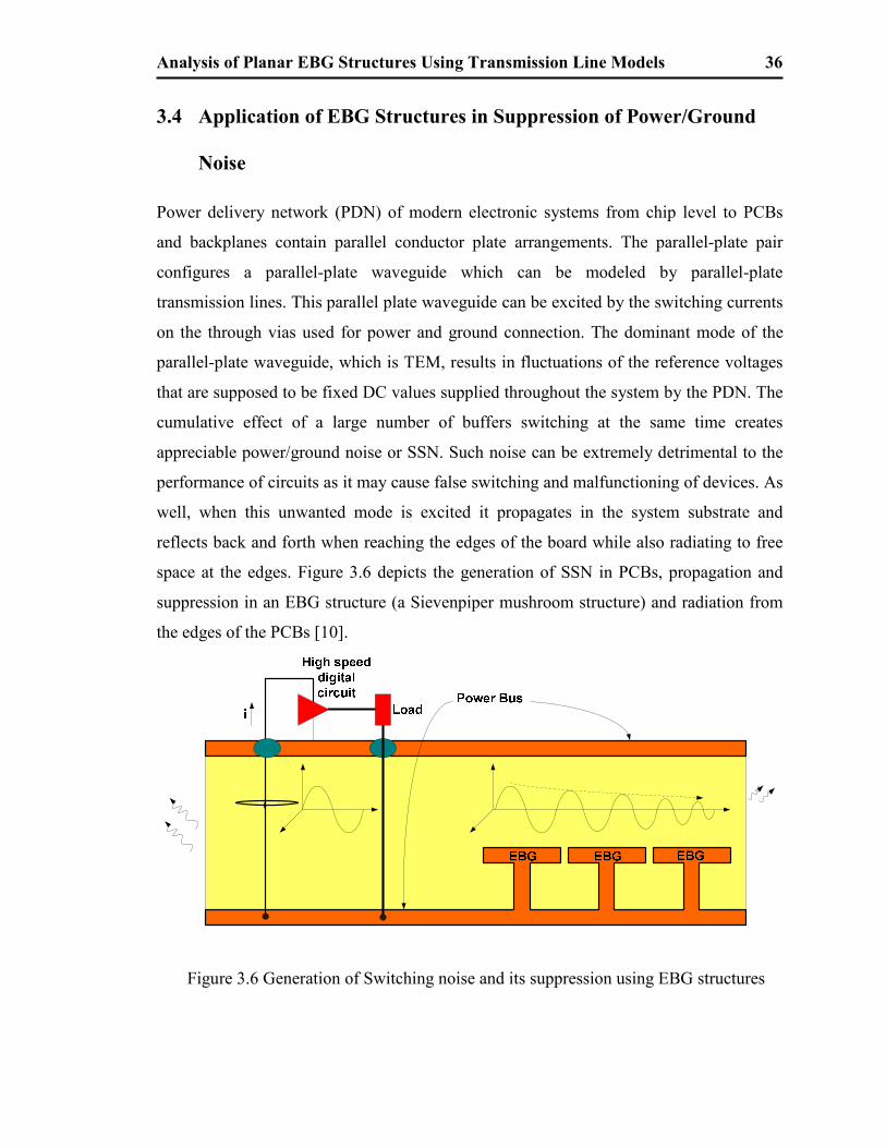
3.4 Application of EBG Structures in Suppression of Power/Ground
Noise
Power delivery network (PDN) of modern electronic systems from chip level to PCBs
and backplanes contain parallel conductor plate arrangements. The parallel-plate pair
configures a parallel-plate waveguide which can be modeled by parallel-plate
transmission lines. This parallel plate waveguide can be excited by the switching currents
on the through vias used for power and ground connection. The dominant mode of the
parallel-plate waveguide, which is TEM, results in fluctuations of the reference voltages
that are supposed to be fixed DC values supplied throughout the system by the PDN. The
cumulative effect of a large number of buffers switching at the same time creates
appreciable power/ground noise or SSN. Such noise can be extremely detrimental to the
performance of circuits as it may cause false switching and malfunctioning of devices. As
well, when this unwanted mode is excited it propagates in the system substrate and
reflects back and forth when reaching the edges of the board while also radiating to free
space at the edges. Figure 3.6 depicts the generation of SSN in PCBs, propagation and
suppression in an EBG structure (a Sievenpiper mushroom structure) and radiation from
the edges of the PCBs [10].
Figure 3.6 Generation of Switching noise and its suppression using EBG structures
Analysis of Planar EBG Structures Using Transmission Line Models 37
In the following subsections, we discuss various methods that have been tried to mitigate
the adverse effects of SSN, one of the most prevalent problems faced today by integrated
circuits (ICs) operating at higher frequencies with lower power supply voltages.
3.4.1 Use of Discrete Decoupling Capacitors
One of the most popular noise suppression methods involves the use of decoupling
capacitors [59]-[65]. Decoupling capacitors provide a shorting path for the SSN. The
capacitor has connecting leads for attachment to the PDN. The inductance associated
with the lead of the decoupling capacitors creates a self resonant frequency, thereby
decreasing the effectiveness of the capacitor dramatically beyond this frequency [66].
The effectiveness of the capacitor can be increased by various means which include
placing more decoupling capacitors closer to the chip [67], connecting the decoupling
capacitors directly to the power and ground planes through vias rather than traces since
the trace loop adds to the inductance. There are approaches to optimize the values and
location of the decoupling capacitor [29], [66], which include placing the decoupling
capacitors closer to the device power/ground pins [68].
However, the effectiveness of decoupling capacitors is basically in the low operating
frequency regions (in the sub 600 MHz range).
3.4.2 Use of Embedded Capacitors
Another method involves the use of embedded capacitors to suppress power ground noise
[69], [70]. This method has been found to very effective in the suppression of ground
bounce noise up to 5GHz [71], [72]. The effectiveness of this method depends heavily
upon the dielectric constant of the substrate and hence places a bottleneck on the
performance of embedded capacitors. Very high dielectric constant substrates have been
used to increase the capacitance between the layers [73] but the problem with such high
permittivity dielectrics is that they are not as cost effective as discrete decoupling
capacitors.
Analysis of Planar EBG Structures Using Transmission Line Models 38
3.4.3 Use of Shorting Vias and Islands
This method uses shorting vias and virtual island- like patches to block SSN from
reaching sensitive devices. The shorting vias provide a low impedance path to the
returning current and the islands stop the propagation of PPW noises through the
power/ground pair in the PCB’s. In this method too, noise suppression is achievable only
over a very narrow frequency range [74].
3.5 Other Applications of EBG Structures
As stated earlier, one of the main applications of EBG structures is as a reflective HIS.
HISs are used in antenna applications and also in miniaturization of circuit components
like printed inductors [75].
In these applications, the HISs behave as an artificial magnetic conductor (AMC).
Whenever an antenna is placed in close proximity to an AMC surface, a part of the
antenna signal is radiated and part of it is directed towards the AMC surface and gets
reflected. When the antenna is placed close to a conductor reflector, it can technically be
shorted as the reflection from the ground plane would interfere destructively with the
radiated wave and result in a deterioration of the radiation pattern and cancellation of it in
the extreme case. An AMC, surface on the other hand results in no phase change in the
reflected wave and hence, this reflected wave interferes constructively with the radiated
wave from the antenna to give an improved radiation pattern.
High impedance surfaces acting as AMC conductors have an additional advantage too. In
addition to providing a scenario for constructive interference, these surfaces have
forbidden bands associated with them. An important property of operation of these
surfaces within the forbidden band is that they stop wave propagation within these bands.
Once this occurs, the surface waves are eliminated within the forbidden band of operation
or are almost negligible. Hence, in the absence of surface waves, the radiation pattern is
further ameliorated [28]. This region of the bandgap where the reflected wave provides
maximum constructive interference with the incident wave can be a subset of the
Analysis of Planar EBG Structures Using Transmission Line Models 39
bandgap itself [76]. As discussed in [76], when a reflected signal is evaluated at a
distance d from a reflective plane, the reflection phase introduced due to a regular and
non patterned continuous metal ground plane is given by,
•−= 360180λ
φ d (degrees) (3.43)
When the continuous metal plane is replaced by an EBG plane, the reflection phase for
the reflected wave is given by,
( )
∫
∫=
S
SSCATTERED
EBGdSs
dSEPhase
ˆφ (3.44)
where SCATTEREDE is the scattered E field data from an incident wave s and S is surface
over which the phase needs to be evaluated.
3.6 Conclusion
In this chapter, an overview of EBG structures and the various geometries associated with
them are presented. The concept of surface waves and the various modes that come into
existence in periodic structures are discussed. The correlation of these modes with
Maxwell’s equations and the methodology behind capturing the modal characteristics are
introduced. The concept of SSN and methods, particularly the use of EBG structures, to
mitigate SSN are also discussed. The chapter also deals with other applications of EBG
structures such as their use as AMC surfaces for antenna applications.
Analysis of Planar EBG Structures Using Transmission Line Models 40
CHAPTER 4 Modeling using Transmission
Line Circuit
Most EBG structures used in microwave filtering applications consist of two conductors
in which one is the reference conductor also acting as a shield. In PDNs and multilayer
circuits, we generally encounter at least three conductor layers. The focus of this thesis is
on the two metal layer structures as they can be modeled using conventional transmission
line circuits. These structures are mainly composed of microstrip line sections. In order to
better understand the characteristics of EBG structures realized using microstrip lines, we
need to analyse the operation of a microstrip line. In this chapter, a review of a microstrip
line is presented followed by the modeling of EBG structures. Then, a stepped impedance
EBG structure is analyzed.
4.1 Analysis of a Single Microstrip Line
Microstrip lines are widely used as interconnects of choice due to their ease of
fabrication. A microstrip line consists of a conductor placed over a grounded dielectric
substrate. The important geometrical parameters in the design of the microstrip line are
its width ( )W , length ( )L , distance from the ground plane ( )b and the relative permittivity
of the dielectric medium ( )rε . The fundamental characteristics of the microstrip line, 0Z
and β , depend upon the width of the microstrip line and the relative permittivity of the
substrate. This can observed from the expressions discussed later under this section.
Since the electromagnetic wave supported by a microstrip line is exposed to two different
dielectric media, the microstrip line supports a quasi-TEM wave.
Figure 4.1: Cross section of a microstrip line configuration
Analysis of Planar EBG Structures Using Transmission Line Models 41
Figure 4.2: Important parameters and port definition for the analysis of a microstrip line
Based on [13], [77] references, the effective dielectric constant of a microstrip line is
given by
≤
−+
+
−+
+
>
+
−+
+
=
bW for
bW
Wb
bW for
Wb
rr
rr
e
1104.0
121
12
12
1
1
121
12
12
1
2εε
εε
ε (4.1)
Same references provide the following formulas for the characteristic impedance of the
microstrip line
>
+++
≤
+
=1
444.1ln667.0393.1
120
141
8ln60
0
bW for
bW
bW
bW for
bW
Wb
Z
e
e
ε
πε
(4.2)
To verify the closed-form formulas, the microstrip line is analyzed using ADS LineCalc.
The dimensions of the simulated microstrip line being analyzed are provided in Table
4.1. FR4 is the dielectric substrate. For these design parameters, 1>bW
, and Equations
(4.1) and (4.2) yield the DC effective dielectric constant of, 3426.30, =effε F/m, and a
characteristic impedance, 89.480 =Z Ω .
The frequency dependent characteristic impedance of a microstrip line as provided in
[78] is given by
Analysis of Planar EBG Structures Using Transmission Line Models 42
−
−
=
1
1
0,
,
5.0
,
0,0,0
eff
Feff
Feff
effF ZZ
ε
ε
ε
ε (4.3)
where Feff ,ε is the frequency dependent effective dielectric constant.
Table 4.1: Microstrip line parameters
Parameter Value Units
Width of the Microstrip line W 10 Mil
Thickness of the Microstrip line t
1.3 Mil
Distance from the ground plane b
5 Mil
Permittivity of the medium rε 4.4 None
Length of the Mcrostrip line L 100 Mil
Modifying (4.3) in order to calculate Feff ,ε yields
a
acbbFeff 2
42
,
−±−=ε (4.4)
where 1=a
+−−−=
0,
20,
220,
20, 22
eff
effeffeff kkkb
ε
εεε
1=c
0
,0
Z
Zk F=
Choosing only the addition in the numerator of the RHS of Equation (4.4), the frequency
dependent Feff ,ε can be calculated.
The most accurate way to find characteristic impedance and permittivity of a microstrip
line is by conducting full-wave simulations which provide these parameters as functions
of frequency. Hence, the microstrip described in Table 4.1 was simulated using two main
Analysis of Planar EBG Structures Using Transmission Line Models 43
microwave circuit simulators; Ansoft’s High Frequency Structure Simulator (HFSS) and
Agilent’s Advanced Design Systems (ADS). ADS is a 2.5-D solver based on the method
of moments (MoM). By 2.5-D it is meant that only 2D planar layouts and particular
vertical conductor structures like vias can be simulated. This allows for stacking up of
one layer above another but not a structure with 3D complexities. ADS is widely used to
analyze planar circuits like microstrip- or stripline-based geometries. HFSS is a 3D field
solver operating based on the finite element method (FEM) for the numerical analysis. It
is a robust and accurate software that enables the analysis of complex 3D geometries.
FR4 was used as the dielectric substrate.
One of the most important steps in the design process using HFSS is the definition of the
ports. A wave port is commonly chosen for the excitation. HFSS generates a solution by
exciting each wave port individually. Each mode incident on a port contains one Watt of
time-averaged power. Care has to be taken in defining the ports as wrong field excitation
at the port can lead to incorrect results. In the conducted simulations, the height of the
port is chosen to be approximately ten times the height of the substrate and the width was
chosen to be approximately fifty percent of the dielectric width. This definition is in
accordance with the recommended guidelines of the simulator. Another important feature
is the definition of the radiation boundary. Since most of the designs discussed in this
thesis are open boundary problems and hence radiation boundaries are used to emulate a
wave radiating infinitely far into space. It does so by essentially absorbing the wave at the
radiation boundary thereby distending the boundary to theoretical infinity.
Figure 4.3(a) shows the layout of a microstrip line in HFSS. Figure 4.3(b) shows the field
distribution when a waveport is used for excitation. It clearly depicts the quasi-TEM
nature of the wave supported by the microstrip line. Figure 4.4 (a) depicts the frequency
dependent effective relative permittivity and Figure 4.4 (b) shows the plot of the
characteristic impedance of the microstrip line and its variation with frequency. Three
methods are used to derive the results of Figure 4.4; HFSS, ADS Momentum and the web
calculator from [77].
Analysis of Planar EBG Structures Using Transmission Line Models 44
Figure 4.5 shows the return loss and insertion loss of the studied microstrip line found
from three methods, HFSS, ADS Momentum, ADS Schematic window simulations
which uses library models for the transmission lines as opposed to full-wave simulations.
It is observed at low frequencies, the microstrip line transmits almost all the power from
the source to the load. This behaviour changes with the increase in frequency; the power
at the load end is always lesser than the power at the source end. This is attributed to the
radiation, conductor and dielectric losses.
Figure 4.3: (a) Simulation setup for the analysis of a microstrip line, and (b) field
distribution corresponding to excitation of a microstrip line
(a) (b)
Figure 4.4: Variation of (a) effective dielectric constant, and (b) characteristic impedance
with frequency. The WebCalculator results are from [77]
Analysis of Planar EBG Structures Using Transmission Line Models 45
Figure 4.5: (a) Return loss, and (b) insertion loss of the studied microstrip line
Radiated power or electromagnetic interference at high frequencies can be a serious
problem as it can affect the performance of the circuit as well as those of the adjacent
circuits. This has been discussed in detail in [79].
4.2 Analysis of 1D and 2D EBG Structures Made with Two Conductor
Transmission Line Circuits
As indicated in the introduction of this chapter, many of the EBG structures used in
microwave and electronic engineering are designed by using transmission line circuits.
The focus of study in this thesis is on the structures containing two conductor layers. In
this chapter mainly the stepped impedance type EBG structures are considered for
modeling and analysis using transmission line network theory and Floquet’s Theorem.
Using these analytical procedures, the characteristic equation or dispersion equation can
be obtained which provides the information about the excited modes and their
propagation constants.
Analysis of Planar EBG Structures Using Transmission Line Models 46
A good understanding can be obtained by first analysing a 1D EBG structure. The two
dimensional periodic structure can then be treated as a deduction of the one dimensional
geometry.
4.2.1 Derivation of Dispersion Equation: 1D Stepped Impedance Structure
Figure 4.6 depicts a one dimensional periodic structure with the period. When this
structure is based on transmission line structures, the voltage and current relationships
according to Floquet’s Theorem are given by
dnn eVV γ−
+ =1 (4.5)
dnn eII γ−
+ =1 (4.6)
To showcase the derivation of the dispersion equation of a one dimensional periodic
structure, a 1D stepped impedance filter also known as hlZZ (Z-low Z-high) filter is
considered. The unit cell has been divided into three sections (refer to Figure 4.7). Then,
the transfer matrix of each section is cascaded with the transfer matrix of the subsequent
section (refer Figure 4.8) to obtain a single equivalent transfer matrix for the unit cell.
Figure 4.6: One dimensional representation of a periodic structure
lZDC
BA
hZDC
BA
hZDC
BA
Figure 4.7: Unit Cell of a 1D stepped impedance filter
Analysis of Planar EBG Structures Using Transmission Line Models 47
Figure 4.8: Cascading of ABCD matrices of sections
From the analysis of microstrip lines, we know that a narrow section has higher
characteristic impedance than a wider section. Hence the parameters of the transmission
line-based unit cell are as follows,
Impedance of the broad section = LZ Ω
Impedance of the narrow section = HZ Ω
Admittance of the broad section = L
L ZY
1= 1−Ω
Admittance of the narrow section = H
H ZY
1= 1−Ω
Length of the sections 1 and 3 (the two narrow sections on either side) = 1d
Length of the section 2 (the broad section in the middle) = 2d
Relative permeability of the medium = rµ
Relative permittivity of the medium = rε
Permittivity of the medium 0.εεε r=
Permeability of the medium 0.µµµ r=
Where 0ε is the permittivity of free space = 121085.8 −× 24-1-3 Askgm
0µ is the permeability of free space = -7104 ×π -2N.A
Intrinsic impedance of the medium εµη .=
Wave Number ηπ f..2k =
Where ‘f’ is the operational frequency
Electrical length of the narrow sections = 11 k d×=θ
Electrical length of the broad section = 22 k d×=θ
The transfer or ABCD matrices of the narrow and wide sections are
Analysis of Planar EBG Structures Using Transmission Line Models 48
X = ( ) ( )( ) ( )
11
11
cossin
sincos
θθθθ
H
H
jY
jZ (4.7)
Y = ( ) ( )( ) ( )
22
22
cossin
sincos
θθθθ
L
L
jY
jZ (4.8)
where X and Y denote the transfer matrices of the high impedance and low impedance
sections, respectively.
The ABCD matrix of the unit cell is, therefore
DC
BA= X*Y*X (4.9)
The Voltage and Current at the beginning and the end of a unit cell are defined using
matrices,
+
+
1
1&n
n
n
n
I
V
I
V respectively
=
∴
+
+
1
1
n
n
n
n
I
V
DC
BAI
V (4.10)
Using Floquet’s Theorem:
dnn eVV γ−
+ =1 (4.11)
dnn eII γ−
+ =1 (4.12)
Hence the (4.10) can be rewritten as,
=
+
+
+
+
1
1
1
1
n
nd
n
dn
I
V
DC
BA
eI
eVγ
γ
(4.13)
Rearranging the above equation yields,
01
1 =
−
−
+
+
d
d
n
n
eDC
BeAI
Vγ
γ
(4.14)
( )( ) 0=−−−⇒ BCeDeA dd γγ
( ) 02 =+−+−⇒ dd eDAeBCAD γγ (4.15)
For a reciprocal network
1=−⇒ BCAD (4.16)
Therefore (4.15) becomes,
( ) 01 2 =+−+⇒ dd eDAe γγ
( )DAee dd +=−⇒ − γγ
Analysis of Planar EBG Structures Using Transmission Line Models 49
( ) ( )DA +=⇒ dcosh2 γ
( ) ( )2
dcoshDA +
=⇒ γ
+=⇒ −
2coshd 1 DA
γ
( )
+=+⇒ −
2coshd 1 DA
jβα (4.17)
( )dreal γα =⇒ d (4.18)
( )dimaginary γβ =⇒ d (4.19)
This analytical derivation is clearly explained in [13]
4.2.2 Derivation of Dispersion Equation: 2D Stepped Impedance Structure
The transmission line model (TLM) developed in the one dimensional problem above can
be extended to the two dimensional geometry as well. The two dimensional
implementation of the transmission line model is discussed in detail in [80]-[84] . These
ideas have also been extended to multilayered and multiconductor geometries [35], [85]-
[87]. In references [36], [81], [88], these models are combined with Bloch-Floquet
Theorem and derivation of 2D dispersion equation is presented [88].
To showcase these derivations again a sample 2D EBG structure composed of dissimilar
transmission line sections shown in Figure 4.9 is analyzed. The length of the unit cell is
a and the length of the broad section of microstrip line is 2d . The length of the narrow
transmission line sections is thus,
−=
22
1
dad .
The model consists of transmission line sections in two perpendicular directions as shown
by overlapping circuit on the 2D stepped impedance structure depicted in Figure 4.9 .
Each transmission line section is represented by its corresponding Transfer matrix as
follows
=
)cos()sin(
)sin()cos(
11
11
ddjY
djZdT
ddh
dhdh ββ
ββ (4.20)
Analysis of Planar EBG Structures Using Transmission Line Models 50
where dβ is the phase constant of the transmission line section. This matrix pertains to
the narrow transmission line segments, thus it is referred to as high impedance TL section
represented by the subscript h in the equation.
lZ
lZ
lZ lZ
hZ
hZ
hZ hZ xx’
y
y’
xI
xVyI y
V
ax
xeI β−
ax
xeV β−a
yy
eI
β−
ay
ye
Vβ
−
[ ]ixT
[ ]oxT
[]i yT
[]
o yT
a
d2
d1
Figure 4.9: A unit cell of a 2D EBG structure and its equivalent transmission line network
Similarly, the transfer matrix of the wider section is represented by
=
)cos()sin(
)sin()cos(
22
22
ddjY
djZdT
ddl
dldl ββ
ββ (4.21)
where dβ is the phase constant of the transmission line section and is considered
identical for both the transmission line sections as the substrate of all the transmission
line sections is the same. The overall transmission matrix of each section composed of
the high and low impedance transmission lines is found from
Analysis of Planar EBG Structures Using Transmission Line Models 51
lhik
ik
ik
iki
k TTDC
BAT =
= (4.22)
hlok
ok
ok
okO
k TTDC
BAT =
= (4.23)
where the superscript i represents the input segment, o represents the output segment in
case different transmission lines are used in the input and output sections as labelled in
Figure 4.9. Note that there are two directions of propagation, x and y, which follow a
similar derivation process to obtain the transfer matrices. Thus index k is included in the
formulations where yxk ,= represents the direction along the axes under consideration.
The transmission line model constructed based on this analysis for structure of Figure 4.9
is depicted in Figure 4.10
yV
ay
yeV γ−
yI
ay
yeI γ−
ax
xeV γ−
ax
xeI γ−
xI
xV
lhik TTT ⋅= hl
ok TTT ⋅=
ixT
iyT
oxT
oyT
zT
Figure 4.10: Four port network representation of a unit cell of a two dimensional periodic
structure
An infinite periodic structure can be viewed as a repetitive array of one such unit cell in x
and y directions. By applying the Bloch-Floquet theorem in both directions and thereby
Analysis of Planar EBG Structures Using Transmission Line Models 52
relating the voltages and current at one port to the voltages and current at other port along
the same axis, similar to what presented for the 1D structure, dispersion equation can be
found. Note: here the Floquet’s phase progression along the x and y directions is
determined by axβ and bxβ factors and denoted by axe β− and aye β− in the following
equations. In addition to this, Kirchhoff’s Voltage Law (KVL) and Kirchhoff’s Current
Law (KCL) are applied to establish the voltage and current relationships at the
intersection of the x and y directed circuits. The following equations are the result of
these calculations,
( ) ( ) 0=−∆−−∆ −−x
aox
ix
ixx
aox
ix
ix IeBBVeAD xx ββ (4.24)
( ) ( ) 0=−∆−−∆ −−y
aoy
iy
iyy
aoy
iy
iy IeBBVeAD yy ββ (4.25)
( ) ( ) ( ) ( ) 0=−−+ −−−−y
aoyy
aoyx
aoxx
aox IeBVeAIeBVeA yyxx ββββ (4.26)
( ) ( )( ) ( ) 0=−∆−−∆−
−∆+−∆−−
−−
yao
yiy
iyyx
aox
ix
ix
yao
yiy
iyx
aox
ix
ix
IeDAIeDA
VeCCVeCCyx
yx
ββ
ββ
(4.27)
where ik
ik
ik
ik
ik CBDA −=∆ , yxk ,= and xβ , yβ represent the phase constants along x and
y axes, respectively.
Eliminating xI , yI from Equations (4.32) to (4.35) we obtain the simplified system of
linear homogenous matrix equation
( ) 022
11 =
=
y
x
yx
yx
y
x
V
V
gg
gg
V
VG (4.28)
where
aai
kok
ik
ik
ok
ok
ik
kk
ke
eBBDBAB
g ββ
−−∆+
+=1 (4.29)
( )
aik
ok
ik
aik
ok
ok
ik
ik
ok
ok
ik
aik
ok
kk
kk
eBBeDDAABCBCe
g β
ββ
−
−−
∆++++−∆∆+
=2
2
1 (4.30)
where ok
ok
ok
iok
ok CBDA −=∆ , yxk ,= . These formulations are fully derived and explained
in [88].
From Equation (4.28) it can be observed that the solution to the matrix equation is
possible if either the determinant of the voltage matrix is zero, or if the determinant of the
Analysis of Planar EBG Structures Using Transmission Line Models 53
coefficient G matrix is zero. For a non-trivial solution we conclude that ( ) 0det =G .
Solving for this condition, we obtain the following dispersion equation
( ) ( ) ( )
( ) ( )21 2sin2sin2
cos2coshcosh
ddZZ
ZZ
aaa
ddl
h
h
l
dyx
ββ
βββ
−−+
=+
(4.31)
where 21 22 dda += . Losses are ignored in this analysis; hence, the attenuation constant
is neglected. The general dispersion equation including losses is:
( ) ( ) ( )
( ) ( )21
21
2sin2sin2
22cos2coshcosh
ddZZ
ZZ
ddaa
ddl
h
h
l
ddyx
γγ
γγγγ
−−+
+=+
(4.32)
where xxx jβαγ += , yyy jβαγ += represent the propagation constants along x and y
axes, respectively.
4.3 Dispersion Diagrams
The dispersion diagram, also known as β−k diagram, is obtained from dispersion
equation. For a 1D periodic structure, this diagram is simply a β−k diagram and β is
the propagation constant along the direction of repetition, k is the wavenumber in the
medium for propagation of light. When the structure is periodic along 2 or 3 directions
plotting such a β−k diagram is complicated. Hence, Brillouin Diagrams are used which
were originally introduced by Leon Brillouin. Based on the directions of propagation, and
propagation constants along those directions and lattice of periodic structures, Brillouin
identified zones to cluster directions of propagations. These zones are studied in detail in
[89]. The 2D periodic structures studied in this thesis are symmetric with respect to x and
y axes and have a square lattice structure. According to Brillouin, all possible directions
of propagation in x and y directions can be combined in an irreducible Brillouin zone
[90]. The irreducible zone for the studied structures is a triangular wedge with ( )th8/1 the
area of a square, i.e. the full Brillouin zone. The method of selection of the triangular
irreducible Brillouin zone from the deducted square reciprocal lattice has been discussed
in detail in [90]. Figure 4.11 shows a diagram of the irreducible Brillouin zone. This
Analysis of Planar EBG Structures Using Transmission Line Models 54
figure shows all the possible values of phase constants along x and y directions. For
plotting a 2D dispersion equation such as Equation (4.31), the possible values for xβ and
yβ are found from the limits set by the irreducible Brillouin zone.
yβ
xβ
yβ
xβ
β
y
x
+
=
y0xββ x +=
yβ
xd
βy
+=π
Γ Χ
Μ
yβ-
xβ-
dπ
−
dπ
0
0,dπ
d
,dππ
d
,0π
dπ
−
dπ
Figure 4.11: Irreducible Brillouin zone of an isotropic square reciprocal lattice with
lattice constant d
Plotting the 2D dispersion diagram involves three major steps [91]
• The phase constant along the perpendicular direction y is fixed at 0 degrees.
Correspondingly, the phase constant along x direction, the base of the Brillouin
triangle, called Χ−Γ direction, is varied from 0 to 180 degrees. Then, from
numerical simulations or calculations of the dispersion equation the first set of
Eigen mode frequencies are found. This generates the frequency dataset for the
wave propagation in the Χ−Γ segment of the Brillouin triangle.
• The phase constant along the Χ−Γ segment of the Brillouin triangle, x direction,
is then fixed at 180 degrees and the phase constant along the Μ−Χ segment, y
Analysis of Planar EBG Structures Using Transmission Line Models 55
direction, is varied from 0 to 180 degrees. Then, from simulations or calculation
of dispersion equation the second set of Eigen mode frequencies are found
• The phase constant along both the segments, Χ−Γ and Μ−Χ , are varied in
synchronization with each other from 180 to 0 degrees. Hence, the third set of
eigenmode frequencies are found for the Γ−Μ segment of the Brillouin triangle.
Generally dispersion diagrams also contain the light line which indicates the propagation
behaviour of light in Χ−Γ and Γ−Μ directions.
The dispersion diagram can be obtained from the numerical codes with eigen value
solvers. The dispersion equations provided in this thesis are found from transmission line
models thus predict the TM modes and lose accuracy as the frequency goes up. The
numerical methods are more accurate as they provide eigen values for all possible modes,
TE and TM. Ansoft HFSS or CST Microwave Studio Suite are the only popular CAD
tools with such capability. CST Studio Suite seems to be more preferred over HFSS for
closed structures as it is comparatively faster. However, the drawback associated with
CST Microwave Studio Suite is its inability to simulate open structures which are very
essential for antenna applications. Ansoft HFSS can predict the dispersion diagram for
both open and closed structures, although it can be a bit tedious and requires a clear
insight into the method of obtaining the dispersion diagram. This enables the user to
optimize the results and obtain accurate results. A detailed approach for generating
dispersion diagrams with Ansoft HFSS is discussed in [76] . Once the dispersion diagram
is obtained, the filtering characteristics are predicted from the bandgap regions between
the β−k curves of various modes for all the phase combinations according to the
irreducible Brillouin zone.
As indicated earlier in 2D dispersion diagrams the light lines are plotted in regions. They
are very important in the sense that they are the boundaries of slow-wave (surface wave)
region. The slope of these light lines marks the propagation velocity. For the waves
bound by the substrate (surface waves), the speed is less than that of a light propagating
in a homogeneous medium. Hence, in the 2D transmission line based structures studied in
this thesis, the waves are bound to the transmission line.
Analysis of Planar EBG Structures Using Transmission Line Models 56
4.4 Planar EBG Structures Based on Stepped Impedance Design
Planar EBG structures are via-less structures. They have the distinct advantage of the
ease of fabrication over structures containing via-holes (Textured EBG structures). Planar
EBG structures essentially consist of a patterned power/ground plane backed by a layer
of dielectric substrate that may be grounded. A surface wave can easily propagate
through such structures owing to their behaviour as a dielectric slab waveguide [92].
Planar EBG structures have been investigated in [1], [3], [93]-[95] .
In the following sections, the studied 1D and 2D EBG structures which are based on a
stepped impedance structure are described and their design parameters are presented.
Dispersion diagram of these structures are generated following the procedure explained
earlier. The studied geometries has DC connectivity and can be considered to have a low
pass configuration, hence, a passband exists at low frequencies.
4.4.1 Studied 1D Stepped Impedance Structure
A 1D stepped impedance filter is designed based on the lookup tables given in [13]. It
can be realized by cascading alternate high and low impedance sections. This in turn can
be achieved by either introducing a variation in the widths of the sections or a variation in
the effective dielectric constant [96] or a combination of both. In the present studied case,
a stepped impedance filter uses wide microstrip lines to approximate shunt capacitors and
narrow lines to approximate series inductors in order to provide a lowpass frequency
response. Two such stepped impedance filter designs are investigated in [36]. In this
thesis Design A is considered for evaluations. Design A has the following parameters:
10W1 = mm, 5.0W2 = mm and 6g = mm. Rogers RO3010 with a thickness h of 1.27
mm is used as the substrate of choice with thickness t of the copper cladding being 0.017
mm. Hence, the total length of the edges of the unit cell a is 16 mm. Figure 4.12 shows
the layout of Design A with its equivalent transmission line circuit.
Analysis of Planar EBG Structures Using Transmission Line Models 57
hZ hZlZ
2.10=rε
air
1.27h (mm)
10d2 (mm)
62d1 (mm)
10.2εr (RO3010)
½ (17)t (oz (um))
0.5W2 (mm)
10W1 (mm)
Design A
Parameter
1.27h (mm)
10d2 (mm)
62d1 (mm)
10.2εr (RO3010)
½ (17)t (oz (um))
0.5W2 (mm)
10W1 (mm)
Design A
Parameter
Figure 4.12: (a) Unit cell of a one dimensional stepped impedance filter, (b)Design
parameters, and (c) The equivalent transmission line model.
Equation (4.17) is the dispersion equation for this planar 1D structure. Based on this, the
dispersion diagram for the design is generated and compared with its corresponding
dispersion diagram obtained using a full wave solver.
Since the structure is periodic in one dimension, propagation vector assumes the form
xkk x= . Phase is varied along x-axis, Χ−Γ direction, from 0 to 180 degrees and the
corresponding eigenfrequencies are obtained. Figure 4.13 (a) and Figure 4.13 (b) depict
the dispersion diagrams obtained using the code developed based on calculation of
Equation (4.17) (let us refer to this as transmission line modeling method or TLM for
brevity) and by using a full wave solver, respectively.
From the two figures it can be observed that the dispersion diagram obtained from the
full wave solver predicts a higher number of modes. Plotting the light line divides this
diagram into two distinct regions known as the fast wave region (lying above the light
line) and the slow wave region (lying below the light line). The portion of the
eigenmodes lying above the light line represents the portion of the eigenmodes that are
not bound to the surface and are radiative in nature. These waves are known as leaky
Analysis of Planar EBG Structures Using Transmission Line Models 58
waves [28]. The modes that lie above the light line can radiate energy away by coupling
to the external plane waves (when the EBG surface is used as reflector in antenna
applications). They are radiatively unstable and have an imaginary frequency component.
Below the light line are the waves that are bound to the substrate and closer to what is
predicted by the transmission line modeling method.
4.4.2 Predicting the Insertion Loss Information from the Dispersion
Equation
By modifying the TLM based code, the S21-parameter characteristic of a finite size
structure composed of n unit cells can be predicted. This can be achieved by the
following relation
( )( )nd rfeS ˆ21 log20 ⋅−= α (4.33)
where n is the number of unit cells included between the two measurement ports, ( )fα is
the frequency dependent attenuation constant and d is the lattice constant and 21S is
expressed in decibel. The attenuation constant for the different frequency points is infact
obtained from the complex propagation constant found from Equation (4.17). Basically it
is β in the stopband.
To obtain other scattering parameters one can obtain the equivalent transfer matrix of the
n unit cells by cascading the transfer matrices of all the cells between the ports
converting them to scattering parameter matrix.
The insertion loss plots obtained by different methodologies, from full-wave HFSS, ADS
Momentum and TLM method are depicted in Figure 4.13 (c). It can be observed that a
very good match is found between the results obtained using the TLM based code and the
full wave analysis.
Analysis of Planar EBG Structures Using Transmission Line Models 59
Table 4.2 presents the numerical values of the stopband predicted from the results shown
in Figure 4.13 (a) and (b).
(a)
(b)
Analysis of Planar EBG Structures Using Transmission Line Models 60
(c)
Figure 4.13: (a) Dispersion diagram from TLM based code, (b) Dispersion diagram from
full wave solver (c) Insertion loss for a finite structure consisting of three unit cells
Table 4.2: Comparison between the stopbands found from TLM code and full wave
solver (HFSS) results for 1D stepped impedance based EBG design
EBG geometry
Bandgap from TLM based code
( )codeBW
(GHz)
Bandgap from full wave solver (HFSS)
( ) wavefullBW
(GHz)
Time to simulate the results using TLM based code
Time to simulate the results using HFSS
Percentage match in bandgap
100BW
BW
code
wavefull ×
Design A
1.49~4.149
1.662~3.969
107 seconds
1 hour and 52 minutes
86.8
4.4.3 Studied 2D Stepped Impedance Structure
Having analysed the one dimensional stepped impedance filter, the same design
specifications are extended to a two dimensional geometry. In fact the studied layout is
Analysis of Planar EBG Structures Using Transmission Line Models 61
the structure shown in Figure 4.9. The analysis of the structure follows the same pattern
as discussed for a one dimensional stepped impedance filter with the sectioning of the
unit cell being the only exception. The one dimensional structure consisted of 3 sections
for the analysis whereas the two dimensional structure, owing to its symmetry about the
x- and y-axes, is split into four sections. The same method could have been applied to the
one dimensional structure too, considering the unit cell is symmetrical about a transverse
axis (in our case the y-axis) passing through the center of the unit cell. However, for ease
of calculation, a three section method was followed. Figure 4.14 shows the cross section
of a transmission line model for the unit cell of this 2D structure along one direction to
show the segmentation used for the analysis. The four port network representation of the
unit cell is shown in Figure 4.10.
Employing the methodology discussed in section 4.2.2, the dispersion equation for the
planar 2D EBG structure shown in Figure 4.9 is given by
( ) ( ) ( )
( ) ( )( )11
dyx
WsinWsin2
cos2coscos
−
−−
+=+
aZZ
ZZ
aaa
ddl
h
h
l ββ
βββ
(4.34)
where lZ and hZ are the characteristic impedances of the broad and narrow transmission
line sections, respectively. The effective dielectric constant and characteristic impedance
of a microstrip line is given by (4.1) and (4.2), respectively.
The stopband obtained by this EBG structure can be considered to be omni-directional as
it occurs in all azimuthal directions of propagation.
Figure 4.15 and Figure 4.16 present a comparison between the dispersion diagrams
obtained using the TLM method and a full wave solver (HFSS), respectively. Table
presents the numerical values of the bandgap predicted from the results shown in Figure
4.15 and Figure 4.16
Analysis of Planar EBG Structures Using Transmission Line Models 62
2.10=rεmm 27.1h =
1=rε
Figure 4.14: Cross section of the TL model of the 2D stepped impedance EBG structure
Figure 4.15: Dispersion diagram of the 2D stepped impedance structure based on
Design A predicted by the TLM code
Analysis of Planar EBG Structures Using Transmission Line Models 63
Figure 4.16: Dispersion diagram of the 2D stepped impedance structure based on Design
A obtained from HFSS full-wave solver
4.4.4 Insertion Loss Simulation and Measurement
The insertion loss information is obtained from the scattering parameter S21. In order to
extract the values of S21 using the TLM method, the same approach that has been applied
to the 1D EBG design is employed for the 2D EBG design. This involves generating the
equivalent transfer matrix for n unit cells between two ports on the EBG structure and
then carrying out the conversion from the transfer matrix to the scattering parameter
matrix. Once the scattering parameter matrix is obtained, the S21 values are easily
extracted from it.
Another method to obtain the scattering parameters is by conducting a measurement on
the fabricated structure. The EBG structure used for insertion loss simulation and
Analysis of Planar EBG Structures Using Transmission Line Models 64
measurement, is shown in Figure 4.17. The figure also denotes the location of the vertical
SMA connectors used for excitation. Anritsu’s 37397D Vector Network Analyzer (VNA)
(Lightning, 40MHz to 65 GHz) is used for measuring the scattering parameters and from
the recorded data, the S21 information is extracted and plotted.
The insertion loss plot in Figure 4.18 depicts the results obtained from using different
methods, including full wave simulation results, along with the S21 results of a parallel-
plate structure which is used as a reference. Port 1 is located at ( )mm 72,mm 40 and Port
2 is located at ( )mm 72,mm 120 .
Port 1
Port 2
Figure 4.17: Illustration of the EBG structure constituted of several cascaded unit cells
along with the port definitions for the calculation of the Insertion Loss
Analysis of Planar EBG Structures Using Transmission Line Models 65
Figure 4.18: Magnitude of S21 for finite size stepped impedance structure for the
arrangement shown in Figure 4.17 and calculated between 28 segments along x-direction
Table 4.3: Comparison between the TLM code and full wave solver results
EBG geometry
Bandgap from TLM based code
( )codeBW
(GHz)
Bandgap from full wave solver HFSS
( ) wavefullBW
(GHz)
Time to simulate the results using TLM based code
Time to simulate the results using HFSS
Percentage match in bandgap
100BW
BW
code
wavefull ×
Design A 1.49~4.151
2.368~3.836
115 seconds 3 hours and 36 minutes
55.1672
Analysis of Planar EBG Structures Using Transmission Line Models 66
4.5 Conclusion
In this chapter, we analysed the behaviour of a microstrip line as this is the TL of our
choice for realising the various EBG geometries discussed in this thesis. We also
introduced the concept of using transmission line model (TLM) for the analysis of 1D
and 2D two conductor EBG structures. The methodology behind the analysis was
discussed in detail. We discussed the method of extraction of the modal characteristics of
the EBG structures discussed in this thesis within a defined irreducible Brillouin zone. A
stepped impedance based EBG structure was investigated in order to validate the results
obtained using the TLM based code and verify its accuracy with respect to results
obtained from full wave analysis.
The only drawback with the TL modeling is that only TM (Transverse Magnetic) modes
of propagation are captured but not the TE (Transverse Electric) modes.
Analysis of Planar EBG Structures Using Transmission Line Models 67
CHAPTER 5 Design and Modeling of
Meander lines
As discussed in Section 3.3 of Chapter 3, an EBG structure can be approximated by an
effective surface impedance and the centre frequency can be estimated by LC and the
width of the bandgap is related to CL . Hence, it can be inferred that in order to
achieve a bandgap at lower frequencies with a wide bandwidth, methods for increasing
the effective inductance of the unit cell should be employed. In the planar EBG structures
reported in [3], [38], [94], [95], a meander line is used to connect microstrip line sections,
instead of the high impedance transmission line section shown in Figure 4.9 of Chapter 4.
The meander line increases the inductance of the unit cell which in turn reduces the lower
edge of the bandgap. Application of this method results in the achievement of ultra-
wideband noise suppression as reported in [3].
In this chapter we review the methodology behind obtaining the lumped component
model of a meander line so that it may be effectively employed in a TLM of an EBG
structure consisting of metal patches connected by meander lines.
5.1 Inductance of the Meander Line
The layout of a typical meander line is shown in Figure 5.1. To extract the equivalent
inductance of a meander line, its layout is decomposed into straight conductive segments.
The total inductance is found from the sum of the self inductances of all the segments and
the mutual inductances between all combinations of the straight segments.
5.1.1 Calculation of Self Inductance
The self inductance of a straight conductor with a rectangular cross section as shown in
Figure 5.2 is given in [97], [98] by the following formula
+++
+
⋅⋅=3l
tw0.50049
tw2l
lnl0.002L (5.1)
Analysis of Planar EBG Structures Using Transmission Line Models 68
Figure 5.1: Various segments of a meander line for the calculation inductance
Figure 5.2: A conducting segment of a meander line
where L is the inductance in Hµ , l is the length, w is the width and t the thickness of the
conducting segment in centimeters. The above equation is valid for materials with a
magnetic permeability equal to unity and the inductance is assumed to be frequency
independent. The closed form equation provides a cumulative self inductance due to both,
the internal and the partial external inductance of an element.
As an example let us consider the meander inductor geometry shown in Figure 5.1
Figure 5.3: Middle segments used for the calculation of inductances
Analysis of Planar EBG Structures Using Transmission Line Models 69
The total self inductance of all the segments is given by
dhbaselftot 1)L(NNL2L2LL ++++= (5.2)
where dhbaL ,,, are self inductances of segments with lengths dhbal ,,,= respectively.
N- Number of segments of greatest length h (which for the geometry shown in
Figure 5.3 and Figure 5.3 is 6)
5.1.2 Calculation of Mutual Inductance
The general equation for the mutual inductance of the segments with equal length l and
separated by a distance r is given by
Figure 5.4: Mutual inductance of two equal parallel straight filaments
+
+−
++⋅⋅±=lr
lr
1rl
1rl
lnl2πµ
r)(l,M22
0c (5.3)
Mutual inductance between unequal filaments intersecting at a point at an angle θ is
given by [97]
( ) HS
tanhS
tanh0.002cosM 11 µθ
++
+= −−
yx
yxy
x (5.4)
Figure 5.5: Two intersecting unequal filaments inclined at an angle θ [97]
Analysis of Planar EBG Structures Using Transmission Line Models 70
Mutual inductance between two unequal filaments in the same plane not meeting at any
point is given by [97]
Figure 5.6: Two non-intersecting unequal filaments inclined at an angle θ [97]
( ) ( ) ( )
( ) ( )
+−
+−
++
+
++=
−−
−−
32
1
43
1
41
1
21
1
SStanh
SStanh
SStanh
SStanh0.002cosM
xy
xy
yx
νµ
νµθ
(5.5)
where
( ) ( )[ ]
422
223
24
2223
22
2
4SSSS2
αα
µ−
−−+−−=
yxxyxy
(5.6)
( ) ( )[ ]
422
223
22
2223
24
2
4SSSS2
αα
ν−
−−+−−=
yxyxyx
(5.7)
21
22
23
24
2 SSSS −+−=α (5.8)
From (5.4) and (5.5), we conclude that mutually perpendicular segments exhibit no
mutual inductance. Figure 5.1 shows the meander line geometry in addition to the various
parameters that were used for the calculation of inductance.
Mutual inductance of other segments can be expressed using the above expressions. In
[98] various scenarios are discussed. The expressions for calculating the mutual
inductance in each case are presented herein.
Analysis of Planar EBG Structures Using Transmission Line Models 71
Figure 5.7:Two parallel segments displaced by a finite distance
For the arrangement shown in Figure 5.7, the mutual inductance between the two