SURFACE SCIENCE 30 (1972) 53-68 0 North-Holland Publishing Co. ANALYTICAL AND EXPERIMENTAL INVESTIGATION OF THE EFFECTS OF OXYGEN CHEMISORPTION ON THE ELECTRICAL CONDUCTIVITY OF CdS* SUPRASAD BAIDYAROY** and PETER MARK Department of Electrical Engineering, Princeton University, Princeton, New Jersey 08.540, U.S.A. Received 16 September 1971; revised manuscript received 12 November 1971 An investigation of the effects of surface states on the equilibrium conductivity of thin, wide bandgap semiconductors is presented. A comparison of measured conductivities with those computed from different surface state models (discrete or distributed), chosen a priori, reveals that the oxygen chemisorption states of natural surfaces of CdS (single crystals and evaporated films) are distributed in energy. An exponential distribution of the form Ds(E) = Noexp[(E-E&WC] give the best agreement between theory and experiment. 1. Introduction There have been numerous studies eliciting the effects of chemisorption on the electrical conductivity of thin samples (single crystals and films) of semiconductors, especially wide bandgap (> 2 eV) compound semicon- ductorsl). As compound semiconductors tend to be self_compensated2), they are frequently insulating and chemisorption may have an enormous effect on their electronic properties. Most of the investigations have been carried out with the chemisorption of acceptor-like adsorbates (e.g., oxygen, halogens) on n-type adsorbents (e.g., CdS, ZnO) where chemisorption is manifest, among other ways, in the reduction of both photo and equilibrium conductivities, sometimes by several decades. Considerable effort has been made to locate the energy level(s) of the chemisorbed ions with respect to the band structure of the adsorbent. However, a complete characterization of surfaces states is difficults~~) because the bulk properties of the material must be completely specified and because the data analysis invariably involves extensive numerical computations that cannot, as yet, yield a unique surface state distribution from the experimental results596). At present, the experimental data are best interpreted by comparison with theoretical modeling calculations. * Supported by the Office of Naval Research and by the National Science Foundation. ** Part of Ph.D. dissertation. 53
Department of Electrical Engineering, Princeton University, Princeton, New Jersey 08.540, U.S.A.
Received 16 September 1971; revised manuscript received 12 November 1971
An investigation of the effects of surface states on the equilibrium conductivity of thin, wide bandgap semiconductors is presented. A comparison of measured conductivities with those computed from different surface state models (discrete or distributed), chosen a priori, reveals that the oxygen chemisorption states of natural surfaces of CdS (single crystals and evaporated films) are distributed in energy. An exponential distribution of the form Ds(E) = Noexp[(E-E&WC] give the best agreement between theory and experiment.
1. Introduction
There have been numerous studies eliciting the effects of chemisorption
on the electrical conductivity of thin samples (single crystals and films) of
semiconductors, especially wide bandgap (> 2 eV) compound semicon-
ductorsl). As compound semiconductors tend to be self_compensated2), they
are frequently insulating and chemisorption may have an enormous effect
on their electronic properties. Most of the investigations have been carried
out with the chemisorption of acceptor-like adsorbates (e.g., oxygen,
halogens) on n-type adsorbents (e.g., CdS, ZnO) where chemisorption is
manifest, among other ways, in the reduction of both photo and equilibrium
conductivities, sometimes by several decades. Considerable effort has been
made to locate the energy level(s) of the chemisorbed ions with respect to
the band structure of the adsorbent. However, a complete characterization
of surfaces states is difficults~~) because the bulk properties of the material
must be completely specified and because the data analysis invariably
involves extensive numerical computations that cannot, as yet, yield a
unique surface state distribution from the experimental results596). At
present, the experimental data are best interpreted by comparison with
theoretical modeling calculations.
* Supported by the Office of Naval Research and by the National Science Foundation. ** Part of Ph.D. dissertation.
53
54 S. RhIDYhROY AND P. MARK
To date, equilibrium conductivity calculations exist oniy for discrete surface states337). However, such a model does not explain all the features of existing ambient-sensitive conductivity data of compound semiconduc- tors, In the case of oxygen on CdS, for example, the slope of the semieon- ductivity {log conductance versus reciprocal temperature) curves increases gradually with increasing oxygen pressure (i.e., with increasing surface state densitysev). The theoretical curves, computed from a discrete surface state model, exhibit onIy two activation energies: One corresponds to the bulk donor levef ~bulk-controlled regime) at low surface state densities and the other, at higher surface state concentrations, is given by the difference between the surface state energy with respect to the conduction band edge and the induced maximum surface potentiai {surface-controlled regime).
This paper discusses the general problem of computing the equilibrium conductivity of a thin, wide bandgap semiconductor for an arbitrary distribu- tion of surface states and compares these results with experiments on vapor- phase-grown CdS crystals with natural surfaces that are disordered (no LEED pattern) and contaminated principally with carbon and chlorine 17, Is), and on evaporated films. Similar measurements on CdS single crystals with ordered and clean surfaces are reported elsewhereis). As most of the chemisorption studies involve acceptor-like adsorbates and n-type adsor- bents, the computations treat this case (and the equivalent case of donor- like adsorbates on p-type adsorbents). The effect of donor-like facceptor- like) surfaces states on an n-type~~type) bulk has been treated elsewhere7+s). Modeling calculations have been performed with uniform, gaussian and exponential surface state distributions but only the exponential distribution is discussed here because it provides the best explanation of the experimental data.
2, Formulation of the surface state problem: acceptor-like surface states cm
n-type bulk
In this section the general surface state problem, with several simplifying assumptions, is set up for an arbitrary distribution of surface state energies in the forbidden gap of the semiconductor bulk, First, it has been assumed that the effective density of states in the conduction band Nc is independent of temperat.ure. Actually Nc is proportional to the three-halves power af temperature (for parabolic bands). Second, the carrier mobility has been assumed to be independent of temperature and pressure; i.e., the con- ductivity is proportional to (n), the average density of free electrons in the conduction band. l’n practice, the mobility can be a function of both temper- ature 9, lo) and pressure 11* i2). The rationale for ignoring the temperature and
OXYGEN CHEMISORPTION AND ELECTRICAL CONLWCTWITY OF CdS 55
pressure dependence of the mobility lies in the fact that mobility changes,
however large, are usually small compared to the change in (n). In thin
insulating platelets of CdS, for example, the equilibrium conductivity in the
presence of oxygen may be as much as 7 decades below the vacuum (< 10M6
torr) value7pia). This change is accompanied by only a 30% reduction in
the Hall mobility ls). In other cases, for instance for chemically spray-
deposited thin films where scattering at the intergrain potential is domi-
nant 11, 12), and when chemisorption is accumulation types), it is less
justifiable to interpret the ambient-sensitive semiconductivity data without
an explicit consideration of the effects of temperature and pressure on the
mobility.
It has also been assumed that the surface state density is independent of
temperature. However, a real surface which is usually heterogeneous in
nature consists of a collection of active centers, each of which may be
characterized by a separate adsorption energy. The statistical distribution
of adsorbates onto these sites is bound to be temperature dependent 14-r6).
Therefore, it is quite possible that the surface state density is temperature
dependent. The chief argument for assuming a temperature independent
surface state density, for that matter also for the other assumptions, is a lack
of experimental data. Present calculations based on these assumptions
explain the existing experimental data quite adequately. Finally, the ad-
sorbate free surface is assumed to have flat bands.
As mentioned earlier, most of the wide bandgap semiconductors, especially
II-VI compounds, tend to be compensatedz). In the present case, the bulk
donors (No) and the partially-compensating acceptors (NA) are assumed to
have discrete energy levels located at energies EC, and EVA from their
respective band edges. When the surface states are occupied by electrons,
t Ds( El
SURFACE STATE DISTRISU- TION
Fig. 1.
t=o t= w
Energy band diagram of an n-type semiconductor (ND > NA) of thickness in the presence of an acceptor-like surface distribution.
2w
56 LBAIDYAROY AND P. MARK
the energy bands bend up, as shown in fig. 1. The negative charge in the surface states is compensated by the positive charge of the uncompensated ionized bulk donors.
For an n-type material, the concentration of the holes in the valence band can be neglected. Furthermore, the acceptors are assumed to be completely
-0;
>
f
- 0.4
G
Ii”
-0.6
I
ll.F -0.8
-I .o
-1.2 I
>_
.5
\
-I I
1
I I I # ,
2.5 3.5 4.5 5.5 6.5
+ x IO 3
J
Fig. 2a
Fig. 2b
OXYGEN CHEMISORPTION AND ELECTRWAL CONDUCTIVITY OF CdS 57
0.1 6
0.06
f x to3
Fig. 2. (a) Log10 <n> versus (l/T) for an n-type semiconductor with an exponential acceptor-like surface state distribution. [ Tc = lOOO”K, ND’ = 2 x 10’2 cm-j; other para-
meters are listed in table 11. (b) Position of Fermi level versus (l/T) corresponding to the curves of (a). (c) Schottky barrier height versus (l/T) corresponding to the curves of (a).
Curve label
TABLE 1
Key to figs. 2, 3 and 4
No{cm-2 eV-I) _~____ Fig. 2 Fig. 3
-- Fig. 4
A < 10” < 3 x 10’0 < 1010
B 3 x 10’1 10’1 3 x 10¹⁰
c 10’2 3 x 10¹¹ 10’1
D 3 x 10’2 1012 3 x 10”
E 1018 3 x 10’2 10’2
F 3 x 10¹³ 1013 3 x 10¹²
G 10’4 3 x 10¹³ -
H 3 x 10¹⁴ 10’4
I 10’5 3 x 10¹⁴ I
J 3 x 10¹⁵ 1015 K 1016 L 3 x 101” -
W= 0.001, ND = 10’6 cm+, &D = 0.2 eV and IC = 10.
58 S. BAIDYAROY AND I’. MARK
filled. Also, since the semiconductor is presumed well-compensated (i.e., Nn= NA, with N,>N,), the Fermi level is expected to remain well below the shallow donor level so that Boltzmann statistics for the occupation of the bulk donors can be used.
The equilibrium conductivity is proportional to (n) which is given byst7)
W
(,,) = !!k; s e-“(Z’ikT &, (1) 0
where W is the half-width of the sample (see fig. 1) and where X=exp ( - [EC (0) - E,JKT) and V(z) is the electrostatic potential. These two para- meters are obtained from a simultaneous solution of the following equations (Appendix A) :
W
XNd s e-v(z)/kT dz = WNi - X s Ds (E) dE
0 x + eWs-E”kT (2)
AEs
and dZV e2 hZ” = iE& N; - Nix ,-“fz)/kr 1 (3)
where N& = NC+ Nn eEcDlkT, NC is the conduction band effective density of states, Nd= Nn- NA, D,(E) is the surface state density of states (non-zero over the interval A&), V,= V(W), K is the adsorbent dielectric constant and se is the free space permittivity. Eq. (2) stems from the over-all charge neutrality condition valid at equilibrium and eq. (3) is Poisson’s equation. Eqs. (l), (2) and (3) h ave been used to compute the conductivity ((n)) of a thin n-type semiconductor for different forms of L+(E): discrete [NsS (E- Es)]; uniform [IN, over A&]; gaussian {No exp[- (Es-E)2/(kTC)Z]); exponential [eq. (4)], and with “reasonable” values of bulk parameters. The case of the exponential surface state energy distribution is singled out for discussion because of its usefulness in the interpretation of the experiments. The uniform and gaussian distributions will be discussed in a later publica- tion and the discrete case has already been discussed in detail elsewherev).
3. Banded surface states with an exponential energy distribution
The surface state distribution considered in this section can be written as
D,(E)=N, eeElkTc cm-’ eV_‘, (4)
OXYGEN CHEMISORPTION AND ELECTRICAL CONDUCTIVITY OF CdS 59
where E is the depth of the level below the conduction band and T, is a characteristic temperature describing the spread of the distribution. The physical plausibility and the main features of such a distribution are discussed in detail in Appendix B.
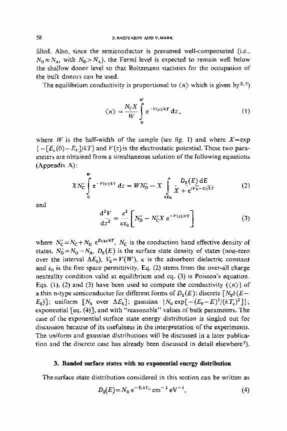
The results of the first sample calculation taking T, = 1000 “K and ND =2 x 10¹², with N, as a parameter, are shown in figs. 2a through 2c. Values for the parameter are fisted in table 1. Fig. 2a is a plot of log,, (n) versus (l/T) with No as a parameter. The most important feature of this plot is a gradual increase in the activation energy with increasing No. The con- ductivity-temperature-N,, curves of this example bear a close resemblance to the conductivity-temperature-pressure measurements of section 4. For low values of N,,, the curves are straight lines in the low temperature region with an activation energy EC, (=0.2 eV), corresponding to the bulk donor level (bulk-controlled regime). At the onset of the surface-controlled regime, which is characterized by an increased activation energy, the slope of the curves increases almost linearly with the logarithm of surface state density (see fig. 5). Fig. 2b shows the position of the Fermi level with respect to the bottom of the conduction band at z=O for the above case. Notice that
I I
9
- A
; e
0
7
3 2.0 3.0 4.0 5.0 6.0 7.0 8.0 9.0
Fig. 3. Log10 <n> versus (l/T) for an n-type ~miconductor with an exponential acceptor- like surface state distrjbution. [Te = lOOO”K, ND’ = 2 x 10¹¹ cmP3; other parameters are
Listed in table 11.
60 S. BAIDYAROY AND P. MARK
as the Fermi level lies well below the bulk donor level, even for N,, =0
(adsorbate free case), the surface states lying in the range E=O to Ez0.3 eV
do not affect the conductivity of the bulk. Thus, it is not possible to deter-
mine the nature of the surface state distribution near the conduction band
edge from conductivity measurements, because these states always lie above
the Fermi level. Fig. 2 shows the surface barrier height corresponding to
the curves of fig. 2a. The barrier height reaches a maximum of 0.18 eV
[ -eNnW2/2rcs,] at the onset of the surface-controlled regime7) (curves
E through L).
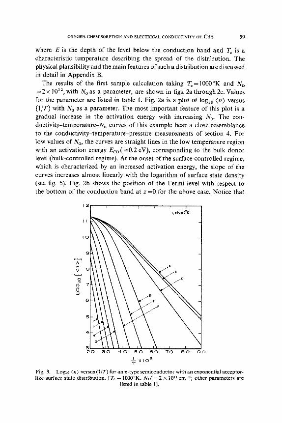
The effects of decreasing Nn are shown in fig. 3 which is a plot of log,, (n)
versus l/T with N,, as a parameter (see table 1 for parameter values), taking
Nn =2 x loll, a decade lower than the example of fig. 2a. The curves of this
figure have all the features of those of fig. 2a. However the following
quantitative differences may be noted:
(i) As a result of decreasing N& fewer electrons are available in the
conduction band; hence, the surface-controlled regime commences at a
lower surface state concentration [e.g., the surface-controlled regime starts
2.0 3.0 4.0 5.0 6.0 7.0 6.0 9.0
Fig. 4. Loglo (n) versus (l/T) for an n-type semiconductor with an exponential acceptor- like surface state distribution. [T, = 3OOO”K, ND’ = 2 x 1Ol2 cm-3; other parameters are
listed in table 11.
OXYGEN CHEMISORPTION AND ELECTRICAL CONDUCTIVITY OF CdS 61
at N,,2:101* for Nd=2x 1O’l (curve Din fig. 3), compared to N,cz~O’~ for
NI; =2 x lo’* (curve E in fig. 2a)].
(ii) For a given Ns (i.e., adsorbate pressure) and T, there is a strong
reduction of (n) with decreasing Nn. For example, with No = 1Ol4 cm-*
eV_’ and l/T=3 x 10m3, (n) = 10” cme3 when Nn=2 x lo’* cme3 (fig. 2a)
and (n) = IO5 cmv3 for Nd =2 x lOi (fig. 3). The physical explanation of
a stronger reduction of (n) with decreasing Nn is as follows: a smaller Nd
is associated with a smaller I’s ( =eN~W2/2rcso); therefore, the transfer of
electrons from the conduction band to the surface states is less retarded
when Nn is small (i.e., when the specimen is well compensated).
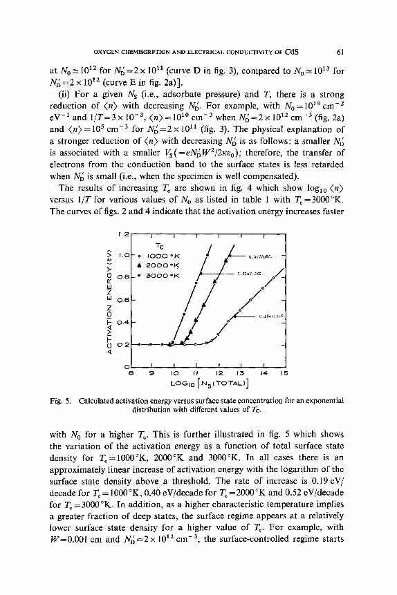
The results of increasing T, are shown in fig. 4 which show log,, (n>
versus l/T for various values of No as listed in table 1 with T, =3000”K.
The curves of figs. 2 and 4 indicate that the activation energy increases faster
Fig. 5.
1.2- I I I I I I
TC
5 1.0-o ,OOOOK %!
1 k 0.4evmc. -
b
A 20000K
0.6 _ l 3000 OK //
O.SZe”,OEC.
9
./- . A
0 I I I I I I
e 9 12 13
&,;~rymLI]
14 15
Calculated activation energy versus surface state concentration for an distribution with different values of Tc.
exponential
with No for a higher T,. This is further illustrated in fig. 5 which shows
the variation of the activation energy as a function of total surface state
density for T,=lOOO”K, 2000°K and 3000°K. In all cases there is an
approximately linear increase of activation energy with the logarithm of the
surface state density above a threshold. The rate of increase is 0.19 eV/
decade for T, = 1000 “K, 0.40 eV/decade for T, = 2000 “K and 0.52 eV/decade
for T, =3000”K. In addition, as a higher characteristic temperature implies
a greater fraction of deep states, the surface regime appears at a relatively
lower surface state density for a higher value of T,. For example, with
W=O.OOl cm and Nd=2 x 10¹² cme3, the surface-controlled regime starts
62 S. BAIDYAROY AND P. MARK
at N,(total)- 1012 cme2 for T, = 1000°K (curve E of fig. 2a) as compared
to N,(total) z 3 x 10” cme2 for T, = 3000 “K (curve C of fig. 4).
4. Effects of oxygen chemisorption on the conductivity of CdS
The effects of oxygen chemisorption on the equilibrium conductivity of
vapor phase-grown CdS single crystals with natural surfaces have been
investigated by Goodwin and Marksy7). These data are explained here on
the basis of the modeling calculations of section 3. Similar ambient-sensitive
conductivity data taken on evaporated thin films of CdS are also reported
here and are similarly interpreted.
The evaporated films (courtesy: Bell and Howell Research Laboratories,
Pasadena, California) were 5 to 10 urn thick and were prepared by evapo-
rating CdS on heated (N 225 “C) glass substrates (3 in. x 2 in.) in a vacuum
of about 10e5 torr. Specimens of size $ in. x f in. were used for electrical
measurements. Ohmic contacts to the films were made by melting indium
in a nitrogen atmosphere. In a room ambient the films were good photo-
conductors.
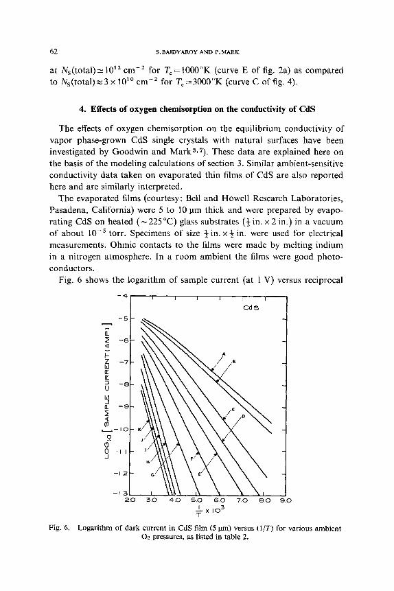
Fig. 6 shows the logarithm of sample current (at 1 V) versus reciprocal
-41------ cds I ii 3 -6-
r
?I -7 -
cc
I _6_ u
“:
P
-s-
$ L-.-IO-
(1” cj -I I-
-l 2 -
-I 3 2.0 3.0 4.0 5.0 6.0 7.0 6.0 9.0
+x IO 3
Fig. 6. Logarithm of dark current in CdS film (5 pm) versus (l/T) for various ambient 0~ pressures, as listed in table 2.
OXYGEN CHEMISORPTION AND ELECTRICAL CONDUCTIVITY OF CdS 63
temperature, with ambient oxygen pressure as a parameter, for an evaporated
CdS film (thickness 5 urn). The data were taken in a stainless steel vacuum
chamber which had a vacuum capability of lo-* torr without a bake-out.
The apparatus and the experimental procedure are described in detail
elsewhere7). The curves of fig. 6 are “fast cooling” curves; i.e., they cor-
respond to rapid cooling of the sample. Curves representing a relatively
“slow” temperature change (heating or cooling) of the sample are similar
to those of fig. 6.
TABLE 2
Key to figs. 6 and 7
Curve label Ambient oxygen pressure (torr)
Fig. 6 Fig. 7 _
A B C D E F G H I J K
4 x 10-s 6 x 1OW 5 x IO-6 5 x IO-5
5 x IO-4
5 x 10⁻³
5 x IO-2
5 x 10-l
5
50
760
< 10-B 3 x 10-S 10-s 3 x 10-s 10-d 10-3
10-Z IO-’ 1 10 102
0
g- -I 5
-I
1.0 30 50 7.0 9.0
+ x IO 3
Fig. 7. Logarithm of dark current in CdS single crystal (20 pm) versus (l/T) for various ambient 02 pressures, as listed in table 2 (ref. 7).
64 S.BAlDYAROY AND P.MARK
It is instructive to compare the ambient-sensitive conductivity data of evaporated thin films with those of single crystals of CdS. Fig. 7 shows a typical family of curves for a crystalline CdS platelet with natural surfaces of approximate size 2 mmx 1 mm x 20 urn. A comparison of these two figures shows that the evaporated films also exhibit the same qualitative ambient-sensitivity as the single crystals: there is a gradual reduction in the conductivity coupled with an increase of activation energy with increasing ambient oxygen pressure. Comparing the experimenta curves figs. 6 and 7 with the computed conductivity curves of section 3, and also with simiiar curves computed with the other us-distributions mentioned earlier, it turns out that an exponential distribution of surface states gives the best agreement between theory and experiment. This conclusion is substantiated further from a comparison of measured and computed activation energies of conductivity.
Fig. 8 is a plot of the activation energy of semiconductivity versus O2 pressure for the crystalline sample. The curve has two linear regions: one with a fixed activation energy of 0.2 eV corresponding to the bulk donor level, and in the other the activation energy increases at the rate of 0.07 eV/ decade increase of 0, pressure. The calculations of section 3 indicate that the activation energy versus log (surface state density) plot for an exponential distribution of surface states have two straight-line segments (fig. 5) which is an additional reason to believe that the oxygen ~hemisorption states have an exponential energy distribution. But it is difficult to assign a characteristic temperature to the distribution. Figs. 5 and 8 show that in order to get a
0.1 ! I I I,,,,,,
-8 -6
LOCIO [GL,, FZSSUR~ ~TORR:]
Fig. 8. Measured activation energy versus ambient oxygen pressure (slopes of the low-T region of the curves of fig. 7).
OXYGEN CHEMISGRFTION AND ELECTRICAL CONDUCTIVITY OF CdS 65
“0.07 eV/decade” change in the activation energy the surface state density must follow the following approximate relations:
Ns (total) oc PI” for T, = 3000”K,
cc P1l6 for T, = 2000”K,
cc PlJ3 for T, = lOOO”K,
where P is the ambient oxygen pressure. If the h$(P) dependence were known (e.g., from the variation of the oxygen Auger electron intensity with oxygen pressure), the characteristic temperature could be determined. From the present experimental data it is not possible to determine either the characteristic temperature or the Ns (P) dependence. Nevertheless, the computations of section 3 and the data presented in figs. 6 and 7 suggest that a distributed model for the chemisorbed oxygen states is better than a discrete modela.7). The physical plausibility for this conclusion is presented in Appendix B.
The conductivity of the films is, however, more “sensitive” to the ambient oxygen pressure. There is noticable reduction in the conductivity even at pressure in the lo-* torr range. For single crystals, there is no significant reduction in the conductivity below low6 torr. This is reasonable. First, the films are “thin” (thickness =5-10 urn, compared to -20 pm for the crystal- line sample) and so have fewer electrons in the conduction band (= WN;)
to be chemisorbed before the conductivity begins to decrease appreciably. Hence, for the thin films the surface-controlled regime is initiated at a lower oxygen pressure. Probably more important, films have heterogeneous sur- faces. It has been shown that CdS (and ZnO) crystals with atomically disordered surfaces are more susceptible to chemisorption than similar crystals with ordered surfaces 17,1s). Thus, even at pressure in the 10m8 torr range, the surface state density is high enough to cause a significant reduction in the conductivity of the evaporated thin films (which are polycrystalline and hence are likely to have strongly disordered surfaces.)
Appendix A
SOLUTION OF POISSON AND CHARGE NEUTRALITY EQUATIONS
The Poisson equation (3) can be written in the following dimensionless form :
d2Y/dY2 = [l - Re-YI(Y)], (A.0
where Y(Y) = V(z)/kT, R = Nix/N& Y=z/L, and Ln = (q,kT/e2ND)*, the Debye length for ionized donors. The maximum value of R is 1 (flat band condition) and the minimum is 0 (corresponding to complete depletion
66 S. BAIDYAROY AND P. MARK
of the conduction band). The numerical evaluation of (A.l) has been dis- cussed in detail by Goodwin and Mark’): given a value of R, !P (Y) can be computed at any Y(z).
The charge neutrality equation (2) can be written as:
x= w
WN,: 3 (A.21
where Y(z) = Y (Y) and Us = Y(W). Here, Y(W) is given by eq. (A. 1). For any chosen value of X, Y(z) can be determined by solving (A. I) and hence (A.2), which can be written in the form X=f (X), can be solved by a digital computer.
Appendix B
CHEMISORPTI~N SURFACE STATES
This Appendix examines the dependence of the energy distribution of the chemisorption states on the surface structure. P~ausibie arguments are given to substantiate an exponential distribution.
The energy distribution of adsorbed ions may be related to the atomic surface structure. Even a perfectly ordered and clean surface cannot be regarded as a continuum but rather as a two dimensional array of inter- acting atoms where the lattice potential varies periodically. The depth of the potential wells may be regarded as the energy of desorption, and should be the same for all the wells of an atomically clean structured surface. For chemisorption, the depth is very large (+kT at room temperature) and adsorption is Localized. If the interaction between adsorbed species is neglected, there should be only one desorption energy, and the adsorption or desorption probability should be the same for all sites. There is evidence that this is so for specially processed ZnO surfacesl’). On the other hand, if the surface is heterogeneous, due to the presence of structural defects or chemical impurities the lattice potential profile at the surface will be irregular. For such disordered and/or contaminated surfaces a range of desorption energies is possibleIs). The energetically lower sites correspond to chemi- sorption and are occupied first, so that the heat of adsorption decreases steadily with increasing surface coverage. The exact energy distribution of the chemisorption sites depends upon the particular surface structure which in turn depends upon surface preparation. For example, in ZnO, the oxygen chemisorption states have a complicated energy distribution when the surface is prepared by mechanica polishing whereas the same nominal
OXYGEN CHEMISORPTION AND ELECTRICAL CONDUCTIVITY OF CdS 67
surface, when prepared by chemical polishing, tends to have a discrete
level 17).
Sips 15916) calculated the statistical distribution of the adsorption sites of
a heterogeneous surface. Assuming a generalized Freundlich isotherm of the
form c
(B.1)
where, B(P) is the ratio of the total number of adsorbed particles to the
number of available sites NO, P is the ambient pressure, and a and c are
constants independent of pressure, he showed that
N (E) = ; ‘$?!f [eEl“T _ 11-c, 03.2)
where N(E)dE is the number of sites whose energy of desorption lies in
the range E and E+dE. For chemisorbed ions, ES kT and eq. (B.2) can
be written as:
N(E) = N, ‘y & e-ElMTld. ( > (B.3)
Eq. (B.3) shows that, at a particular temperature, the chemisorption sites
are exponentially distributed in energy. However, there is also a strong
temperature dependence of N(E), unless c is linearly proportional to
temperature. Nevertheless, in the event of a lack of sufficient information
about the adsorption isotherms of CdS, eq. (B.3) justifies, at least partially,
the distribution D,(E) =N, exp[ - E/kT,] for the chemisorption states.
Such a model is in agreement with the experimental observation that the
activation energy of desorption decreases with increasing surface coverage is).
It also explains the ambient-sensitive conductivity measurements (section 4)
quite adequately. The main features of the exponential distribution are the
following :
(i) It has a maximum at the smallest energy of desorption: there are more
shallow states than deeper ones. Adsorption states with desorption energy
close to zero may be regarded as physically adsorbed. The shallow states
(lying above the Fermi level), however, do not affect the value of (n)
although they might influence the carrier mobility.
(ii) There is no discontinuity in the energy of desorption during transition
from physical adsorption to chemisorption.
The significance of the characteristic temperature T, has already been
discussed in section 3.
S. BAIDYAROY AND P. MARK
References
1) W. H. Brattain and J. Bardeen, Bell System Tech. J. 32 (1953) 1; G. Heiland, Z. Physik 138 (1954) 459; 142 (1955) 415; S. R. Morrison, Advan. Catalysis 7 (1955) 259; S. R. Morrison and P. H. Miller, J. Chem. Phys. 25 (1956) 1064; D. A. Melnick, J. Chem. Phys. 26 (1957) 1136; R. H. Bube, J. Chem. Phys. 27 (1957) 496; F. S. Stone, Advan. Catalysis 13 (1962) 1; G. A. Somorjai, J. Phys. Chem. Solids 24 (1963) 175; P. Mark, J. Phys. Chem. Solids 25 (1964) 911; 26 (1965) 959; 26 (1965) 1767; RCA Rev. 26 (1965) 461; A. L. Robinson and R. H. Bube, J. Electrochem. Sot. 112 (1965) 1002; H. Shear, E. A. Hilton and R. H. Bube, J. Electrochem. Sot. 112 (1965) 997; K. J. Haas, D. C. Fox and M. J. Katz, J. Phys. Chem. Solids 26 (1965) 1779; K. W. Boer and R. Schubert, Phys. Status Solidi 16 (1966) K5; F. B. Micheletti and P. Mark, Appt. Phys. Letters 10 (1967) 136; J. Appt. Phys. 39 (1968) 5274; P. Mark, J. Phys. Chem. Solids 29 (1968) 689.
2) A. G. Fischer, R. E. Schrader and S. Larach, in: Photoelectronic Materials and Devices, Ed. S. Larach (Van Nostrand, New York, 1965) pp. 84-86.
3) P. Mark, Surface Sci. 25 (1971) 192. 4) S. G. Davison and J. D. Levine, in: Solid State Physics, Vol. 25 (Academic Press,
New York, 1970), pp. 1-149. 5) J. D. Levine and S. Freeman, Phys. Rev. B2 (1970) 3255. 6) S. Freeman, Phys. Rev. B2 (1970) 3272. 7) T. A. Goodwin and P. Mark, Progr. Surface Sci 1 (1971) 1. 8) S. Baidyaroy, W. R. Bottoms and P. Mark, J. Phys. Chem. Solids (in press). 9) F. A. Kroger, H. J. Vink and J. Volger, Physica 20 (1950) 1095.
10) R. S. Crandall, Phys. Rev. 169 (1968) 577. 11) F. B. Micheletti and P. Mark, Appl. Phys. Letters 10 (1967) 136. 12) P. A. Thomas, C. Stbenne and M. Balkanski, Rev. Phys. Appt. 5 (1970) 682. 13) P. Mark, J. Phys. Chem. Solids 25 (1964) 911. 14) H. S. Taylor and S. C. Liang, J. Am. Chem. Sot. 69 (1947) 1306. 15) R. Sips, J. Chem. Phys. 16 (1948) 490. 16) R. Sips, J. Chem. Phys. 18 (1950) 1024. 17) J. D. Levine, A. Willis, W. R. Bottoms and P. Mark, Surface Sci. (in press). 18) S. Baidyaroy, W. R. Bottoms and P. Mark, Surface Sci. (in press). 19) J. Horiuiti and T. Toya, in: Solid State Surface Science, Vol. 1, Ed. M. Green (Marcel