LECopyright copy 2012 by American Scientific Publishers
All rights reserved
Printed in the United States of America
Science of Advanced MaterialsVol 4 pp 1013ndash1017 2012
(wwwaspbscomsam)
CdSCdSe Co-Sensitized Solar Cell Prepared byJointly Using Successive Ion Layer Absorptionand Reaction Method and ChemicalBath Deposition ProcessZhou Yang1 2 Qifeng Zhang1lowast Junting Xi1 Kwangsuk Park1Xiaoliang Xu2lowast Zhiqiang Liang1 and Guozhong Cao1lowast
1Department of Materials Science and Engineering University of Washington Seattle WA 98195 USA2Department of Physics University of Science and Technology of China Hefei Anhui 230026 China
ABSTRACT
CdSCdSe quantum dots co-sensitized TiO2 solar cell was prepared by combining the successive ion layerabsorption and reaction (SILAR) method and chemical bath deposition (CBD) method for the fabrication ofCdS and CdSe quantum dots respectively The effect of CdSe deposition time on the solar cell performancewas investigated It was found that the optimized deposition time for CdSe was 3 h yielding solar cell powerconversion efficiency of 33 The methods introduced in this paper are a simple route for the fabrication ofquantum dot-sensitized solar cells with achieving descent power conversion efficiency
Quantum dot sensitized solar cells (QDSCs) has attracteda lot of attentions during the past several years1ndash4 QDSCshave a similar configuration to dye-sensitized solar cells(DSCs) containing a layer of oxide (TiO2 ZnO SnO2 etc)for electron transport sensitizer adsorbed on the oxide forlight harvesting counter electrode and electrolyte that isfilled in the space between the oxide working electrodeand the counter electrode5 Compared with dye moleculesused in DSCs semiconductor quantum dots are advanta-geous for their tunable band gap as a function of the sizeof quantum dots6 high extinction coefficients67 and largeintrinsic dipole moment facilitating charge separation89
Furthermore in view of the multiple exciton generation(MEG) effect in colloidal quantum dots11011 a theoret-ical photovoltaic conversion efficiency (PCE) of QDSCshas been estimated to be as high as 44 which ismuch higher than the Schockley-Queisser limit sim31for single pndashn junction-based semiconductor photovoltaicdevices12 Research in the field of QDSCs has been grow-ing very quickly over the past few years Nowadays
lowastAuthors to whom correspondence should be addressedEmails qfzhanguwashingtonedu (QFZ) xlxuustceducn (XLX)
gzcaouwashingtonedu (GZC)Received 23 February 2012Accepted 26 May 2012
the highest power conversion efficiency (PCE) of QDSCsis around 413ndash16 Although these values are still lowerthan those for DSCs by both drawing lessons from DSCresearch and adopting much more suitable designs in thefabrication it is believed that the efficiency of QDSCscould be further improvedQuantum dots could be grafted on the metal oxide by
two different approaches in situ growth and absorptionof pre-synthetized quantum dot with or without bifunc-tional linker However the latter always shows relativelylow PCE due to the difficulty in achieving sufficient cov-erage of quantum dots onto the oxide film1718 ChemicalBath Deposition1419 (CBD) and Successive Ionic LayerAbsorption and Reaction152021 (SILAR) are methods thathave been extensively employed for in situ growth of quan-tum dots on metal oxide Although size distribution andparticle aggregation are hard to control with these meth-ods the quantum dot coverage and PCE of cells preparedusing these two methods are always better than those ofcells produced by a post-adsorption process CdSCdSequantum dots are conventional components used as sensi-tizer in quantum dot sensitized solar cells13141922 It hasbeen demonstrated that the CdS layer the quality ofwhich has an important impact on the solar cell perfor-mance serves as both seed layer to enhance the growth ofCdSe quantum dots and an energy barrier layer to reduce
Sci Adv Mater 2012 Vol 4 No 10 1947-2935201241013005 doi101166sam20121386 1013
Delivered by Ingenta toGuest User
IP 16611112071Wed 14 Nov 2012 150359
CdSCdSe Co-Sensitized Solar Cell Prepared by Jointly Using SILAR Method and Chemical Bath Deposition Process Yang et alARTIC
LErecombination between the electrons in metal oxide andthe holes in electrolyte1923 As for the growth of CdSquantum dots the SILAR method has been extensivelyadopted to obtain uniform semiconductor coating2124
However the preparation of CdSe quantum dots using theSILAR needs to be carried out under inert condition in aglove box2124 or under high temperature15 Although CBDmethod is somewhat time consuming it can be conductedto deposit CdSe under atmosphere condition2526
In this work the superiorities of SILAR and CBDmethods are combined together to create CdSCdSe co-sensitized QDSCs The CdS layer and the CdSe quantumdots were deposited by using SILAR method and CBDprocess respectively The purpose of using CdS layer wasto enhance the CdSe growth and reduce the deposit timeThe effects of CdSe deposition time on the solar cell per-formance were thoroughly investigated The samples arenamed as S1 S2 etc according to the CBD depositiontime for CdSe as listed in Table I After the growth of CdSand CdSe a ZnS passivation layer was coated to reducethe recombination rate26 Polysulfide electrolyte (10 MNa2S and 1 M S aqueous solution) and Cu2S counter elec-trode were used to test the cell performance A maximumPCE of 33 was obtained under AM 15 illumination(100 mWcm2
2 EXPERIMENTAL DETAILS
The TiO2 film fabricated on fluorine doped tin oxide (FTO)glass substrate was prepared following the methods pre-viously reported2728 For the growth of CdS firstly theTiO2 film was immersed into a 01 M Cadmium nitrate(Cd(NO32 methanol solution for 1 min In this pro-cess Cd2+ will absorb on the TiO2 electrode Then theelectrode was rinsed with methanol to remove the excessCd2+ and dried in air Successively the electrode wasdipped into 01 M sodium sulfide (Na2S) solution con-taining water and methanol (11 vv) for another 1 minThe S2minus will react with the pre-absorbed Cd2+ to formthe CdS Then the electrode was rinsed with methanoland dried in air This procedure was referred to as one
Table I The sensitization parameters of samples
Deposition parameters
Sample SILAR cycle for CBD time forname CdS growth CdSe growth (h)
S1 5 0S2 5 1S3 5 2S4 5 25S5 5 3S6 5 35S7 5 4
SILAR cycle Five cycles were employed to deposit suit-able amount of CdS on the electrode CdSe was depositedon the CdS coated TiO2 electrode by the CBD methodas reported in literatures141926 but with some modifica-tions Briefly 01 M sodium Selenosulphate (Na2SeSO3aqueous 01 M cadmium acetate (Cd(CH2COO)2 aque-ous solution and 02 M trisodium salt of nitrilotriaceticacid (N(CH2COONa)3 solution were mixed together withvolume ratio 111 Then the CdS coated TiO2 electrodewas vertically immersed into the solution for CdSe layerdeposition under dark condition at 22 C A ZnS passi-vation layer was then deposited on the CdSCdSe coatedTiO2 electrode by two SILAR cycles with 01 M Zincnitrate and 01 M Sodium sulfide aqueous solution as theZn2+ and S2minus sources respectively The polysulfide elec-trolyte is composed of 1 M S and 1 M Na2S in deion-ized water A Cu2S electrode fabricated on brass foil wasused as counter electrode of the cell The preparation ofCu2S electrode can be described as follows brass foil wasimmersed into 37 HCl at 70 C for 5 min then rinsedwith water and dried in air After that the etched brassfoil was dipped into the polysulfide solution leading to ablack Cu2S layer formed on the surface of brass foilThe morphology was characterized by using scan-
ning electron microscope (SEM JSM-7000) EDX wasemployed to analyze the element contents The photo-voltaic properties were measured using an HP 4155Aprogrammable semiconductor parameter analyzer underAM 15 simulated sunlight with a power density of100 mWcm2 The active cell area is 032 cm2 and thethickness of the TiO2 film is about 7 m Thermal sci-entific UV-Vis-NIR spectrum meter was used to study theoptical absorption properties of the samples
3 RESULTS AND DISCUSSION
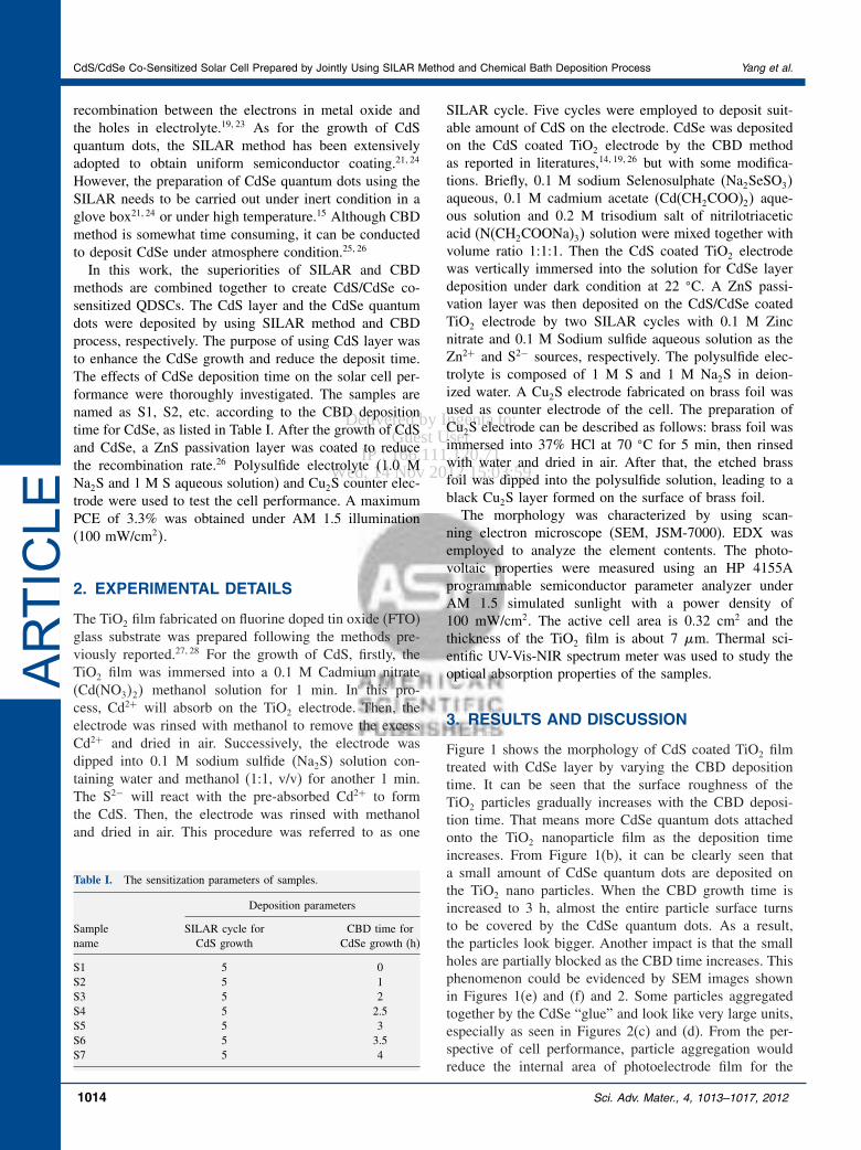
Figure 1 shows the morphology of CdS coated TiO2 filmtreated with CdSe layer by varying the CBD depositiontime It can be seen that the surface roughness of theTiO2 particles gradually increases with the CBD deposi-tion time That means more CdSe quantum dots attachedonto the TiO2 nanoparticle film as the deposition timeincreases From Figure 1(b) it can be clearly seen thata small amount of CdSe quantum dots are deposited onthe TiO2 nano particles When the CBD growth time isincreased to 3 h almost the entire particle surface turnsto be covered by the CdSe quantum dots As a resultthe particles look bigger Another impact is that the smallholes are partially blocked as the CBD time increases Thisphenomenon could be evidenced by SEM images shownin Figures 1(e) and (f) and 2 Some particles aggregatedtogether by the CdSe ldquogluerdquo and look like very large unitsespecially as seen in Figures 2(c) and (d) From the per-spective of cell performance particle aggregation wouldreduce the internal area of photoelectrode film for the
1014 Sci Adv Mater 4 1013ndash1017 2012
Delivered by Ingenta toGuest User
IP 16611112071Wed 14 Nov 2012 150359
Yang et al CdSCdSe Co-Sensitized Solar Cell Prepared by Jointly Using SILAR Method and Chemical Bath Deposition ProcessARTIC
LE
Fig 1 The SEM images of samples (a) S2 (b) S3 (c) S4 (d) S5(e) S6 and (f) S7
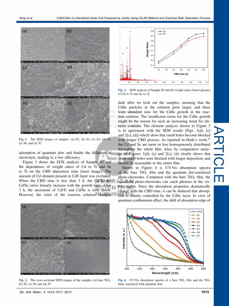
adsorption of quantum dots and hinder the diffusion ofelectrolyte leading to a low efficiencyFigure 3 shows the EDX analysis of Sample S5 and
the dependence of weight ratios of Cd to Ti and Seto Ti on the CBD deposition time (inset image) Theamount of Cd element present in CdS layer was excludedWhen the CBD time is less than 3 h the CdTi andCdSe ratios linearly increase with the growth time After3 h the increment of CdTi and CdSe is slow downHowever the color of the reaction solution changed
Fig 2 The cross-sectional SEM images of the samples (a) bare TiO2(b) S5 (c) S6 and (d) S7
Fig 3 EDX analysis of Sample S5 and the weight ratios (insert picture)of Cd to Ti and Se to Ti
dark after we took out the samples meaning that theCdSe particles in the solution grew larger and therewere abundant ions for the CdSe growth in the reac-tion solution The insufficient room for the CdSe growthmight be the reason for such an increasing trend for ele-ment contents The element analysis shown in Figure 3is in agreement with the SEM results (Figs 1(d) (e)and 2(c) (d)) which show that small holes become blockedwith longer CBD process As reported in Hodersquos work19
the Cd and Se are more or less homogenously distributedthroughout the whole film Also by comparative analy-sis of Figures 1(d) (e) and 2(c) (d) clearly shows thatsome small holes were blocked with longer deposition andshould be reasonable to the entire filmShown in Figure 4 is UV-Vis absorption spectra
of the bare TiO2 film and the quantum dot-sensitizedphoto-electrodes Compared with the bare TiO2 film thesensitized photo-electrodes can catch photons in the vis-ible region Since the absorption properties dramaticallychange with the CBD time it can be deduced that absorp-tion is mainly controlled by the CdSe layer In view ofquantum confinement effect the shift of absorption edge of
Fig 4 UV-Vis absorption spectra of a bare TiO2 film and the TiO2
films sensitized with quantum dots
Sci Adv Mater 4 1013ndash1017 2012 1015
Delivered by Ingenta toGuest User
IP 16611112071Wed 14 Nov 2012 150359
CdSCdSe Co-Sensitized Solar Cell Prepared by Jointly Using SILAR Method and Chemical Bath Deposition Process Yang et alARTIC
LE
Fig 5 Currentndashvoltage (JndashV ) curves for the solar cells correspondingto samples S1 through S7
the photo-electrode moves to the long wavelength with theincrease in CdSe growth period indicating the increase ofthe CdSe particle size The absorption region moves signif-icantly as CBD time is less than 3 h but the change dimin-ishes while the time surpasses 3 h This can be ascribedto the gradually saturated room for the CdSe growthAfter 3 h the absorption edge moves to wavelengtharound 570 nm The size of the quantum dots can be esti-mated using the following equation26
E = E1minusEg =h2
8r2
(1me
+ 1mh
)(1)
where E is the bandgap shift E1 is the bandgap of thequantum dot and could be calculated from the absorptioncurve (218 eV for quantum dots with absorption edge at570 nm) Eg is the bandgap of the bulk materials (174 eVfor CdSe bulk material) me and mh are the effective massof electron and hole respectively For CdSe material theme = 011m0 and mh = 044m0 and m0 is the free electronmass As for E= 0435 eV the calculated radius of CdSequantum dot is 281 nm Therefore it could be deducedthat the holes in TiO2 film with diameter less than 5 nmmay be blocked by the CdSe quantum dot The electrolyteinfiltration will also be hindered to some extent This result
Fig 6 Trend of photovoltaic parameters for samples S1 through S7
is in good agreement with the SEM observation as shownin Figures 1(e) and (f) and 2Figures 5 and 6 present the photovoltaic performance
of the cells with different CdSe deposition time It couldbe clearly seen that the CdSe growth time plays a vitalrole in the cell performance Rapid increments in bothJsc and efficiency during the first 2 h could be observedThis coincides with the growth of the CdSe processas shown in Figure 2 Following this step incrementalincreases of Jsc slowed down while Voc showed small signsof decrease The increase in photocurrent due to quantumdot absorption and the decrease in open circuit voltagedue to increased recombination rate (note the reason willbe explained later) compete each other and jointly deter-mine the solar cell efficiency resulting in a maximum effi-ciency corresponding to a certain deposition time Fromresults gathered in this report a maximum efficiency of33 was attained as for samples with 3 h CdSe depositiontime A similar conclusion was also reported in Mengrsquoswork25 however the maximum efficiency was achievedat the CBD time of 11 h The reduction of reaction timein our experiment should be ascribed to the higher reactiontemperature which will accelerate chemical reaction Thistrend of PCE increasing and then decreasing with CdSedeposition time could be interpreted as follows In the firststage there is an increase in both the amount and sizeof the quantum dots That means more photons and thephotons with lower energy can be captured by the CdSesensitizer as revealed in Figure 4 The absorption intensityincreases and the absorption onset shifts to long wave-length Consequently more electrons will be injected intoTiO2 layer which makes the Jsc increase dramatically andproduces a higher Voc Secondly as the size of the quantumdots becomes larger the electron injection process takesmore time explaining why the sensitizer actually absorbsmore photons however there is no obvious increment in JscFurther increasing quantum dot size may increase recom-bination rate between the electron in quantum dots and theoxidized species in electrolyte As a result the Voc decreasea little Moreover as more and more CdSe quantum dotsare grated on the TiO2 surface the CdSe quantum dotsaggregate together and some holes of the film are blocked
1016 Sci Adv Mater 4 1013ndash1017 2012
Delivered by Ingenta toGuest User
IP 16611112071Wed 14 Nov 2012 150359
Yang et al CdSCdSe Co-Sensitized Solar Cell Prepared by Jointly Using SILAR Method and Chemical Bath Deposition ProcessARTIC
LEThe photo excited carriers in the inner quantum dot layercould not be extracted effectively In addition more andmore crystal boundaries are formed as aggregation of theCdSe quantum dots takes place which will form a lot ofrecombination centers and increase the loss of the photogenerated carriers2329 As a result both the Jsc and Voc
decrease dramatically as the CBD process longer than acertain time for example 3 h The same trend was alsoreported by Toyoda group232930 The poor infiltration ofelectrolyte as a result of pores in the nanocrystalline filmbeing blocked also brings about negative effects on theperformance of the QDSCs
4 CONCLUSIONS
The CdS layer in the CdSCdSe co-sensitized solar cellwas deposited by SILAR method and the CdSe werecoated on the CdS layer by CBD method It was found thatthe CdSe growth time played an important role in deter-mining the overall efficiency of solar cell The depositiontime affected the thickness of CdSe which in turn influ-enced optical absorption and electrolyte penetration of thephoto-electrode An optimized PCE of 33 was attainedin our experiment with a 3 h CBD deposition for CdSe
Acknowledgment This work related to the fabrica-tion and characterization of quantum dot-sensitized solarcells is supported by the US Department of EnergyOffice of Basic Energy Sciences Division of MaterialsSciences under Award no DE-FG02-07ER46467 (QFZ)The device fabrication and optimization is also sup-ported in part by the National Science Foundation (DMR1035196) and the Royalty Research Fund (RRF) fromthe Office of Research at University of Washington ZhouYang would also like to acknowledge the fellowship fromChina Scholarship Council
References and Notes
1 A J Nozik Physica E 1ndash2 115 (2002)2 P V Kamat K Tvrdy D R Baker and J G Radich Chem Rev
11 6664 (2010)
3 S Ruumlhle M Shalom and A Zaban Chem Phys Chem 11 2290(2010)
4 I Mora-Sero and J Bisquert J Phys Chem Lett 20 3046 (2010)5 Q Zhang and G Cao Nano Today 1 91 (2011)6 W W Yu L Qu W Guo and X Peng Chem Mat 14 2854 (2003)7 P Wang S M Zakeeruddin J E Moser R Humphry-Baker
P Comte V Aranyos A Hagfeldt M K Nazeeruddin andM Graumltzel Adv Mater 20 1806 (2004)
8 R Vogel K Pohl and H Weller Chem Phys Lett 3ndash4 241 (1990)9 R Vogel P Hoyer and H Weller J Phys Chem 12 3183 (1994)10 V I Klimov J Phys Chem B 34 16827 (2006)11 R D Schaller M Sykora J M Pietryga and V I Klimov Nano
Lett 3 424 (2006)12 M C Hanna and A J Nozik J Appl Phys 7 074510 (2006)13 M A Hossain J R Jennings Z Y Koh and Q Wang ACS Nano
4 3172 (2011)14 X Huang S Huang Q Zhang X Guo D Li Y Luo Q Shen
T Toyoda and Q Meng Chem Commun 9 2664 (2011)15 Y L Lee and Y S Lo Adv Funct Mater 4 604 (2009)16 M Seol H Kim Y Tak and K Yong Chem Commun 30 5521
(2010)17 I Robel V Subramanian M Kuno and P V Kamat J Am Chem
Soc 7 2385 (2006)18 S Gimenez I Mora-Sero L Macor N Guijarro T Lana-Villarreal
R Gomez L J Diguna Q Shen T Toyoda and J Bisquert Nano-technology 29 292504 (2009)
19 O Niitsoo S K Sarkar C Pejoux S Ruumlhle D Cahen andG Hodes J Photochem Photobiol A-Chem 2ndash3 306 (2006)
20 C H Chang and Y L Lee Appl Phys Lett 5 053503 (2007)21 H Lee M Wang P Chen D R Gamelin S M Zakeeruddin
M Graumltzel and M K Nazeeruddin Nano Lett 12 4221 (2009)22 V GonzaIgravelez-Pedro X Xu I N Mora-SeroIgrave and J Bisquert ACS
Nano 10 5783 (2010)23 T Toyoda K Oshikane D M Li Y H Luo Q B Meng and
Q Shen J Appl Phys 11 114304 (2010)24 H J Lee J Bang J Park S Kim and S-M Park Chem Mat
19 5636 (2010)25 S Q Huang Q X Zhang X M Huang X Z Guo M H Deng
D M Li Y H Luo Q Shen T Toyoda and Q B Meng Nano-technology 37 375201 (2010)
26 Q Shen J Kobayashi L J Diguna and T Toyoda J Appl Phys8 084304 (2008)
27 J Xi Q Zhang K Park Y Sun and G Cao Electrochimica Acta5 1960 (2011)
28 C J Barbeacute F Arendse P Comte M Jirousek F LenzmannV Shklover and M Graumltzel J Am Ceram Soc 12 3157 (1997)
29 S Hachiya Y Onishi Q Shen and T Toyoda J Appl Phys5 054319 (2011)
30 Q Shen A Yamada S Tamura and T Toyoda Appl Phys Lett12 123107 (2010)
Sci Adv Mater 4 1013ndash1017 2012 1017
Delivered by Ingenta toGuest User
IP 16611112071Wed 14 Nov 2012 150359
CdSCdSe Co-Sensitized Solar Cell Prepared by Jointly Using SILAR Method and Chemical Bath Deposition Process Yang et alARTIC
LErecombination between the electrons in metal oxide andthe holes in electrolyte1923 As for the growth of CdSquantum dots the SILAR method has been extensivelyadopted to obtain uniform semiconductor coating2124
However the preparation of CdSe quantum dots using theSILAR needs to be carried out under inert condition in aglove box2124 or under high temperature15 Although CBDmethod is somewhat time consuming it can be conductedto deposit CdSe under atmosphere condition2526
In this work the superiorities of SILAR and CBDmethods are combined together to create CdSCdSe co-sensitized QDSCs The CdS layer and the CdSe quantumdots were deposited by using SILAR method and CBDprocess respectively The purpose of using CdS layer wasto enhance the CdSe growth and reduce the deposit timeThe effects of CdSe deposition time on the solar cell per-formance were thoroughly investigated The samples arenamed as S1 S2 etc according to the CBD depositiontime for CdSe as listed in Table I After the growth of CdSand CdSe a ZnS passivation layer was coated to reducethe recombination rate26 Polysulfide electrolyte (10 MNa2S and 1 M S aqueous solution) and Cu2S counter elec-trode were used to test the cell performance A maximumPCE of 33 was obtained under AM 15 illumination(100 mWcm2
2 EXPERIMENTAL DETAILS
The TiO2 film fabricated on fluorine doped tin oxide (FTO)glass substrate was prepared following the methods pre-viously reported2728 For the growth of CdS firstly theTiO2 film was immersed into a 01 M Cadmium nitrate(Cd(NO32 methanol solution for 1 min In this pro-cess Cd2+ will absorb on the TiO2 electrode Then theelectrode was rinsed with methanol to remove the excessCd2+ and dried in air Successively the electrode wasdipped into 01 M sodium sulfide (Na2S) solution con-taining water and methanol (11 vv) for another 1 minThe S2minus will react with the pre-absorbed Cd2+ to formthe CdS Then the electrode was rinsed with methanoland dried in air This procedure was referred to as one
Table I The sensitization parameters of samples
Deposition parameters
Sample SILAR cycle for CBD time forname CdS growth CdSe growth (h)
S1 5 0S2 5 1S3 5 2S4 5 25S5 5 3S6 5 35S7 5 4
SILAR cycle Five cycles were employed to deposit suit-able amount of CdS on the electrode CdSe was depositedon the CdS coated TiO2 electrode by the CBD methodas reported in literatures141926 but with some modifica-tions Briefly 01 M sodium Selenosulphate (Na2SeSO3aqueous 01 M cadmium acetate (Cd(CH2COO)2 aque-ous solution and 02 M trisodium salt of nitrilotriaceticacid (N(CH2COONa)3 solution were mixed together withvolume ratio 111 Then the CdS coated TiO2 electrodewas vertically immersed into the solution for CdSe layerdeposition under dark condition at 22 C A ZnS passi-vation layer was then deposited on the CdSCdSe coatedTiO2 electrode by two SILAR cycles with 01 M Zincnitrate and 01 M Sodium sulfide aqueous solution as theZn2+ and S2minus sources respectively The polysulfide elec-trolyte is composed of 1 M S and 1 M Na2S in deion-ized water A Cu2S electrode fabricated on brass foil wasused as counter electrode of the cell The preparation ofCu2S electrode can be described as follows brass foil wasimmersed into 37 HCl at 70 C for 5 min then rinsedwith water and dried in air After that the etched brassfoil was dipped into the polysulfide solution leading to ablack Cu2S layer formed on the surface of brass foilThe morphology was characterized by using scan-
ning electron microscope (SEM JSM-7000) EDX wasemployed to analyze the element contents The photo-voltaic properties were measured using an HP 4155Aprogrammable semiconductor parameter analyzer underAM 15 simulated sunlight with a power density of100 mWcm2 The active cell area is 032 cm2 and thethickness of the TiO2 film is about 7 m Thermal sci-entific UV-Vis-NIR spectrum meter was used to study theoptical absorption properties of the samples
3 RESULTS AND DISCUSSION
Figure 1 shows the morphology of CdS coated TiO2 filmtreated with CdSe layer by varying the CBD depositiontime It can be seen that the surface roughness of theTiO2 particles gradually increases with the CBD deposi-tion time That means more CdSe quantum dots attachedonto the TiO2 nanoparticle film as the deposition timeincreases From Figure 1(b) it can be clearly seen thata small amount of CdSe quantum dots are deposited onthe TiO2 nano particles When the CBD growth time isincreased to 3 h almost the entire particle surface turnsto be covered by the CdSe quantum dots As a resultthe particles look bigger Another impact is that the smallholes are partially blocked as the CBD time increases Thisphenomenon could be evidenced by SEM images shownin Figures 1(e) and (f) and 2 Some particles aggregatedtogether by the CdSe ldquogluerdquo and look like very large unitsespecially as seen in Figures 2(c) and (d) From the per-spective of cell performance particle aggregation wouldreduce the internal area of photoelectrode film for the
1014 Sci Adv Mater 4 1013ndash1017 2012
Delivered by Ingenta toGuest User
IP 16611112071Wed 14 Nov 2012 150359
Yang et al CdSCdSe Co-Sensitized Solar Cell Prepared by Jointly Using SILAR Method and Chemical Bath Deposition ProcessARTIC
LE
Fig 1 The SEM images of samples (a) S2 (b) S3 (c) S4 (d) S5(e) S6 and (f) S7
adsorption of quantum dots and hinder the diffusion ofelectrolyte leading to a low efficiencyFigure 3 shows the EDX analysis of Sample S5 and
the dependence of weight ratios of Cd to Ti and Seto Ti on the CBD deposition time (inset image) Theamount of Cd element present in CdS layer was excludedWhen the CBD time is less than 3 h the CdTi andCdSe ratios linearly increase with the growth time After3 h the increment of CdTi and CdSe is slow downHowever the color of the reaction solution changed
Fig 2 The cross-sectional SEM images of the samples (a) bare TiO2(b) S5 (c) S6 and (d) S7
Fig 3 EDX analysis of Sample S5 and the weight ratios (insert picture)of Cd to Ti and Se to Ti
dark after we took out the samples meaning that theCdSe particles in the solution grew larger and therewere abundant ions for the CdSe growth in the reac-tion solution The insufficient room for the CdSe growthmight be the reason for such an increasing trend for ele-ment contents The element analysis shown in Figure 3is in agreement with the SEM results (Figs 1(d) (e)and 2(c) (d)) which show that small holes become blockedwith longer CBD process As reported in Hodersquos work19
the Cd and Se are more or less homogenously distributedthroughout the whole film Also by comparative analy-sis of Figures 1(d) (e) and 2(c) (d) clearly shows thatsome small holes were blocked with longer deposition andshould be reasonable to the entire filmShown in Figure 4 is UV-Vis absorption spectra
of the bare TiO2 film and the quantum dot-sensitizedphoto-electrodes Compared with the bare TiO2 film thesensitized photo-electrodes can catch photons in the vis-ible region Since the absorption properties dramaticallychange with the CBD time it can be deduced that absorp-tion is mainly controlled by the CdSe layer In view ofquantum confinement effect the shift of absorption edge of
Fig 4 UV-Vis absorption spectra of a bare TiO2 film and the TiO2
films sensitized with quantum dots
Sci Adv Mater 4 1013ndash1017 2012 1015
Delivered by Ingenta toGuest User
IP 16611112071Wed 14 Nov 2012 150359
CdSCdSe Co-Sensitized Solar Cell Prepared by Jointly Using SILAR Method and Chemical Bath Deposition Process Yang et alARTIC
LE
Fig 5 Currentndashvoltage (JndashV ) curves for the solar cells correspondingto samples S1 through S7
the photo-electrode moves to the long wavelength with theincrease in CdSe growth period indicating the increase ofthe CdSe particle size The absorption region moves signif-icantly as CBD time is less than 3 h but the change dimin-ishes while the time surpasses 3 h This can be ascribedto the gradually saturated room for the CdSe growthAfter 3 h the absorption edge moves to wavelengtharound 570 nm The size of the quantum dots can be esti-mated using the following equation26
E = E1minusEg =h2
8r2
(1me
+ 1mh
)(1)
where E is the bandgap shift E1 is the bandgap of thequantum dot and could be calculated from the absorptioncurve (218 eV for quantum dots with absorption edge at570 nm) Eg is the bandgap of the bulk materials (174 eVfor CdSe bulk material) me and mh are the effective massof electron and hole respectively For CdSe material theme = 011m0 and mh = 044m0 and m0 is the free electronmass As for E= 0435 eV the calculated radius of CdSequantum dot is 281 nm Therefore it could be deducedthat the holes in TiO2 film with diameter less than 5 nmmay be blocked by the CdSe quantum dot The electrolyteinfiltration will also be hindered to some extent This result
Fig 6 Trend of photovoltaic parameters for samples S1 through S7
is in good agreement with the SEM observation as shownin Figures 1(e) and (f) and 2Figures 5 and 6 present the photovoltaic performance
of the cells with different CdSe deposition time It couldbe clearly seen that the CdSe growth time plays a vitalrole in the cell performance Rapid increments in bothJsc and efficiency during the first 2 h could be observedThis coincides with the growth of the CdSe processas shown in Figure 2 Following this step incrementalincreases of Jsc slowed down while Voc showed small signsof decrease The increase in photocurrent due to quantumdot absorption and the decrease in open circuit voltagedue to increased recombination rate (note the reason willbe explained later) compete each other and jointly deter-mine the solar cell efficiency resulting in a maximum effi-ciency corresponding to a certain deposition time Fromresults gathered in this report a maximum efficiency of33 was attained as for samples with 3 h CdSe depositiontime A similar conclusion was also reported in Mengrsquoswork25 however the maximum efficiency was achievedat the CBD time of 11 h The reduction of reaction timein our experiment should be ascribed to the higher reactiontemperature which will accelerate chemical reaction Thistrend of PCE increasing and then decreasing with CdSedeposition time could be interpreted as follows In the firststage there is an increase in both the amount and sizeof the quantum dots That means more photons and thephotons with lower energy can be captured by the CdSesensitizer as revealed in Figure 4 The absorption intensityincreases and the absorption onset shifts to long wave-length Consequently more electrons will be injected intoTiO2 layer which makes the Jsc increase dramatically andproduces a higher Voc Secondly as the size of the quantumdots becomes larger the electron injection process takesmore time explaining why the sensitizer actually absorbsmore photons however there is no obvious increment in JscFurther increasing quantum dot size may increase recom-bination rate between the electron in quantum dots and theoxidized species in electrolyte As a result the Voc decreasea little Moreover as more and more CdSe quantum dotsare grated on the TiO2 surface the CdSe quantum dotsaggregate together and some holes of the film are blocked
1016 Sci Adv Mater 4 1013ndash1017 2012
Delivered by Ingenta toGuest User
IP 16611112071Wed 14 Nov 2012 150359
Yang et al CdSCdSe Co-Sensitized Solar Cell Prepared by Jointly Using SILAR Method and Chemical Bath Deposition ProcessARTIC
LEThe photo excited carriers in the inner quantum dot layercould not be extracted effectively In addition more andmore crystal boundaries are formed as aggregation of theCdSe quantum dots takes place which will form a lot ofrecombination centers and increase the loss of the photogenerated carriers2329 As a result both the Jsc and Voc
decrease dramatically as the CBD process longer than acertain time for example 3 h The same trend was alsoreported by Toyoda group232930 The poor infiltration ofelectrolyte as a result of pores in the nanocrystalline filmbeing blocked also brings about negative effects on theperformance of the QDSCs
4 CONCLUSIONS
The CdS layer in the CdSCdSe co-sensitized solar cellwas deposited by SILAR method and the CdSe werecoated on the CdS layer by CBD method It was found thatthe CdSe growth time played an important role in deter-mining the overall efficiency of solar cell The depositiontime affected the thickness of CdSe which in turn influ-enced optical absorption and electrolyte penetration of thephoto-electrode An optimized PCE of 33 was attainedin our experiment with a 3 h CBD deposition for CdSe
Acknowledgment This work related to the fabrica-tion and characterization of quantum dot-sensitized solarcells is supported by the US Department of EnergyOffice of Basic Energy Sciences Division of MaterialsSciences under Award no DE-FG02-07ER46467 (QFZ)The device fabrication and optimization is also sup-ported in part by the National Science Foundation (DMR1035196) and the Royalty Research Fund (RRF) fromthe Office of Research at University of Washington ZhouYang would also like to acknowledge the fellowship fromChina Scholarship Council
References and Notes
1 A J Nozik Physica E 1ndash2 115 (2002)2 P V Kamat K Tvrdy D R Baker and J G Radich Chem Rev
11 6664 (2010)
3 S Ruumlhle M Shalom and A Zaban Chem Phys Chem 11 2290(2010)
4 I Mora-Sero and J Bisquert J Phys Chem Lett 20 3046 (2010)5 Q Zhang and G Cao Nano Today 1 91 (2011)6 W W Yu L Qu W Guo and X Peng Chem Mat 14 2854 (2003)7 P Wang S M Zakeeruddin J E Moser R Humphry-Baker
P Comte V Aranyos A Hagfeldt M K Nazeeruddin andM Graumltzel Adv Mater 20 1806 (2004)
8 R Vogel K Pohl and H Weller Chem Phys Lett 3ndash4 241 (1990)9 R Vogel P Hoyer and H Weller J Phys Chem 12 3183 (1994)10 V I Klimov J Phys Chem B 34 16827 (2006)11 R D Schaller M Sykora J M Pietryga and V I Klimov Nano
Lett 3 424 (2006)12 M C Hanna and A J Nozik J Appl Phys 7 074510 (2006)13 M A Hossain J R Jennings Z Y Koh and Q Wang ACS Nano
4 3172 (2011)14 X Huang S Huang Q Zhang X Guo D Li Y Luo Q Shen
T Toyoda and Q Meng Chem Commun 9 2664 (2011)15 Y L Lee and Y S Lo Adv Funct Mater 4 604 (2009)16 M Seol H Kim Y Tak and K Yong Chem Commun 30 5521
(2010)17 I Robel V Subramanian M Kuno and P V Kamat J Am Chem
Soc 7 2385 (2006)18 S Gimenez I Mora-Sero L Macor N Guijarro T Lana-Villarreal
R Gomez L J Diguna Q Shen T Toyoda and J Bisquert Nano-technology 29 292504 (2009)
19 O Niitsoo S K Sarkar C Pejoux S Ruumlhle D Cahen andG Hodes J Photochem Photobiol A-Chem 2ndash3 306 (2006)
20 C H Chang and Y L Lee Appl Phys Lett 5 053503 (2007)21 H Lee M Wang P Chen D R Gamelin S M Zakeeruddin
M Graumltzel and M K Nazeeruddin Nano Lett 12 4221 (2009)22 V GonzaIgravelez-Pedro X Xu I N Mora-SeroIgrave and J Bisquert ACS
Nano 10 5783 (2010)23 T Toyoda K Oshikane D M Li Y H Luo Q B Meng and
Q Shen J Appl Phys 11 114304 (2010)24 H J Lee J Bang J Park S Kim and S-M Park Chem Mat
19 5636 (2010)25 S Q Huang Q X Zhang X M Huang X Z Guo M H Deng
D M Li Y H Luo Q Shen T Toyoda and Q B Meng Nano-technology 37 375201 (2010)
26 Q Shen J Kobayashi L J Diguna and T Toyoda J Appl Phys8 084304 (2008)
27 J Xi Q Zhang K Park Y Sun and G Cao Electrochimica Acta5 1960 (2011)
28 C J Barbeacute F Arendse P Comte M Jirousek F LenzmannV Shklover and M Graumltzel J Am Ceram Soc 12 3157 (1997)
29 S Hachiya Y Onishi Q Shen and T Toyoda J Appl Phys5 054319 (2011)
30 Q Shen A Yamada S Tamura and T Toyoda Appl Phys Lett12 123107 (2010)
Sci Adv Mater 4 1013ndash1017 2012 1017
Delivered by Ingenta toGuest User
IP 16611112071Wed 14 Nov 2012 150359
Yang et al CdSCdSe Co-Sensitized Solar Cell Prepared by Jointly Using SILAR Method and Chemical Bath Deposition ProcessARTIC
LE
Fig 1 The SEM images of samples (a) S2 (b) S3 (c) S4 (d) S5(e) S6 and (f) S7
adsorption of quantum dots and hinder the diffusion ofelectrolyte leading to a low efficiencyFigure 3 shows the EDX analysis of Sample S5 and
the dependence of weight ratios of Cd to Ti and Seto Ti on the CBD deposition time (inset image) Theamount of Cd element present in CdS layer was excludedWhen the CBD time is less than 3 h the CdTi andCdSe ratios linearly increase with the growth time After3 h the increment of CdTi and CdSe is slow downHowever the color of the reaction solution changed
Fig 2 The cross-sectional SEM images of the samples (a) bare TiO2(b) S5 (c) S6 and (d) S7
Fig 3 EDX analysis of Sample S5 and the weight ratios (insert picture)of Cd to Ti and Se to Ti
dark after we took out the samples meaning that theCdSe particles in the solution grew larger and therewere abundant ions for the CdSe growth in the reac-tion solution The insufficient room for the CdSe growthmight be the reason for such an increasing trend for ele-ment contents The element analysis shown in Figure 3is in agreement with the SEM results (Figs 1(d) (e)and 2(c) (d)) which show that small holes become blockedwith longer CBD process As reported in Hodersquos work19
the Cd and Se are more or less homogenously distributedthroughout the whole film Also by comparative analy-sis of Figures 1(d) (e) and 2(c) (d) clearly shows thatsome small holes were blocked with longer deposition andshould be reasonable to the entire filmShown in Figure 4 is UV-Vis absorption spectra
of the bare TiO2 film and the quantum dot-sensitizedphoto-electrodes Compared with the bare TiO2 film thesensitized photo-electrodes can catch photons in the vis-ible region Since the absorption properties dramaticallychange with the CBD time it can be deduced that absorp-tion is mainly controlled by the CdSe layer In view ofquantum confinement effect the shift of absorption edge of
Fig 4 UV-Vis absorption spectra of a bare TiO2 film and the TiO2
films sensitized with quantum dots
Sci Adv Mater 4 1013ndash1017 2012 1015
Delivered by Ingenta toGuest User
IP 16611112071Wed 14 Nov 2012 150359
CdSCdSe Co-Sensitized Solar Cell Prepared by Jointly Using SILAR Method and Chemical Bath Deposition Process Yang et alARTIC
LE
Fig 5 Currentndashvoltage (JndashV ) curves for the solar cells correspondingto samples S1 through S7
the photo-electrode moves to the long wavelength with theincrease in CdSe growth period indicating the increase ofthe CdSe particle size The absorption region moves signif-icantly as CBD time is less than 3 h but the change dimin-ishes while the time surpasses 3 h This can be ascribedto the gradually saturated room for the CdSe growthAfter 3 h the absorption edge moves to wavelengtharound 570 nm The size of the quantum dots can be esti-mated using the following equation26
E = E1minusEg =h2
8r2
(1me
+ 1mh
)(1)
where E is the bandgap shift E1 is the bandgap of thequantum dot and could be calculated from the absorptioncurve (218 eV for quantum dots with absorption edge at570 nm) Eg is the bandgap of the bulk materials (174 eVfor CdSe bulk material) me and mh are the effective massof electron and hole respectively For CdSe material theme = 011m0 and mh = 044m0 and m0 is the free electronmass As for E= 0435 eV the calculated radius of CdSequantum dot is 281 nm Therefore it could be deducedthat the holes in TiO2 film with diameter less than 5 nmmay be blocked by the CdSe quantum dot The electrolyteinfiltration will also be hindered to some extent This result
Fig 6 Trend of photovoltaic parameters for samples S1 through S7
is in good agreement with the SEM observation as shownin Figures 1(e) and (f) and 2Figures 5 and 6 present the photovoltaic performance
of the cells with different CdSe deposition time It couldbe clearly seen that the CdSe growth time plays a vitalrole in the cell performance Rapid increments in bothJsc and efficiency during the first 2 h could be observedThis coincides with the growth of the CdSe processas shown in Figure 2 Following this step incrementalincreases of Jsc slowed down while Voc showed small signsof decrease The increase in photocurrent due to quantumdot absorption and the decrease in open circuit voltagedue to increased recombination rate (note the reason willbe explained later) compete each other and jointly deter-mine the solar cell efficiency resulting in a maximum effi-ciency corresponding to a certain deposition time Fromresults gathered in this report a maximum efficiency of33 was attained as for samples with 3 h CdSe depositiontime A similar conclusion was also reported in Mengrsquoswork25 however the maximum efficiency was achievedat the CBD time of 11 h The reduction of reaction timein our experiment should be ascribed to the higher reactiontemperature which will accelerate chemical reaction Thistrend of PCE increasing and then decreasing with CdSedeposition time could be interpreted as follows In the firststage there is an increase in both the amount and sizeof the quantum dots That means more photons and thephotons with lower energy can be captured by the CdSesensitizer as revealed in Figure 4 The absorption intensityincreases and the absorption onset shifts to long wave-length Consequently more electrons will be injected intoTiO2 layer which makes the Jsc increase dramatically andproduces a higher Voc Secondly as the size of the quantumdots becomes larger the electron injection process takesmore time explaining why the sensitizer actually absorbsmore photons however there is no obvious increment in JscFurther increasing quantum dot size may increase recom-bination rate between the electron in quantum dots and theoxidized species in electrolyte As a result the Voc decreasea little Moreover as more and more CdSe quantum dotsare grated on the TiO2 surface the CdSe quantum dotsaggregate together and some holes of the film are blocked
1016 Sci Adv Mater 4 1013ndash1017 2012
Delivered by Ingenta toGuest User
IP 16611112071Wed 14 Nov 2012 150359
Yang et al CdSCdSe Co-Sensitized Solar Cell Prepared by Jointly Using SILAR Method and Chemical Bath Deposition ProcessARTIC
LEThe photo excited carriers in the inner quantum dot layercould not be extracted effectively In addition more andmore crystal boundaries are formed as aggregation of theCdSe quantum dots takes place which will form a lot ofrecombination centers and increase the loss of the photogenerated carriers2329 As a result both the Jsc and Voc
decrease dramatically as the CBD process longer than acertain time for example 3 h The same trend was alsoreported by Toyoda group232930 The poor infiltration ofelectrolyte as a result of pores in the nanocrystalline filmbeing blocked also brings about negative effects on theperformance of the QDSCs
4 CONCLUSIONS
The CdS layer in the CdSCdSe co-sensitized solar cellwas deposited by SILAR method and the CdSe werecoated on the CdS layer by CBD method It was found thatthe CdSe growth time played an important role in deter-mining the overall efficiency of solar cell The depositiontime affected the thickness of CdSe which in turn influ-enced optical absorption and electrolyte penetration of thephoto-electrode An optimized PCE of 33 was attainedin our experiment with a 3 h CBD deposition for CdSe
Acknowledgment This work related to the fabrica-tion and characterization of quantum dot-sensitized solarcells is supported by the US Department of EnergyOffice of Basic Energy Sciences Division of MaterialsSciences under Award no DE-FG02-07ER46467 (QFZ)The device fabrication and optimization is also sup-ported in part by the National Science Foundation (DMR1035196) and the Royalty Research Fund (RRF) fromthe Office of Research at University of Washington ZhouYang would also like to acknowledge the fellowship fromChina Scholarship Council
References and Notes
1 A J Nozik Physica E 1ndash2 115 (2002)2 P V Kamat K Tvrdy D R Baker and J G Radich Chem Rev
11 6664 (2010)
3 S Ruumlhle M Shalom and A Zaban Chem Phys Chem 11 2290(2010)
4 I Mora-Sero and J Bisquert J Phys Chem Lett 20 3046 (2010)5 Q Zhang and G Cao Nano Today 1 91 (2011)6 W W Yu L Qu W Guo and X Peng Chem Mat 14 2854 (2003)7 P Wang S M Zakeeruddin J E Moser R Humphry-Baker
P Comte V Aranyos A Hagfeldt M K Nazeeruddin andM Graumltzel Adv Mater 20 1806 (2004)
8 R Vogel K Pohl and H Weller Chem Phys Lett 3ndash4 241 (1990)9 R Vogel P Hoyer and H Weller J Phys Chem 12 3183 (1994)10 V I Klimov J Phys Chem B 34 16827 (2006)11 R D Schaller M Sykora J M Pietryga and V I Klimov Nano
Lett 3 424 (2006)12 M C Hanna and A J Nozik J Appl Phys 7 074510 (2006)13 M A Hossain J R Jennings Z Y Koh and Q Wang ACS Nano
4 3172 (2011)14 X Huang S Huang Q Zhang X Guo D Li Y Luo Q Shen
T Toyoda and Q Meng Chem Commun 9 2664 (2011)15 Y L Lee and Y S Lo Adv Funct Mater 4 604 (2009)16 M Seol H Kim Y Tak and K Yong Chem Commun 30 5521
(2010)17 I Robel V Subramanian M Kuno and P V Kamat J Am Chem
Soc 7 2385 (2006)18 S Gimenez I Mora-Sero L Macor N Guijarro T Lana-Villarreal
R Gomez L J Diguna Q Shen T Toyoda and J Bisquert Nano-technology 29 292504 (2009)
19 O Niitsoo S K Sarkar C Pejoux S Ruumlhle D Cahen andG Hodes J Photochem Photobiol A-Chem 2ndash3 306 (2006)
20 C H Chang and Y L Lee Appl Phys Lett 5 053503 (2007)21 H Lee M Wang P Chen D R Gamelin S M Zakeeruddin
M Graumltzel and M K Nazeeruddin Nano Lett 12 4221 (2009)22 V GonzaIgravelez-Pedro X Xu I N Mora-SeroIgrave and J Bisquert ACS
Nano 10 5783 (2010)23 T Toyoda K Oshikane D M Li Y H Luo Q B Meng and
Q Shen J Appl Phys 11 114304 (2010)24 H J Lee J Bang J Park S Kim and S-M Park Chem Mat
19 5636 (2010)25 S Q Huang Q X Zhang X M Huang X Z Guo M H Deng
D M Li Y H Luo Q Shen T Toyoda and Q B Meng Nano-technology 37 375201 (2010)
26 Q Shen J Kobayashi L J Diguna and T Toyoda J Appl Phys8 084304 (2008)
27 J Xi Q Zhang K Park Y Sun and G Cao Electrochimica Acta5 1960 (2011)
28 C J Barbeacute F Arendse P Comte M Jirousek F LenzmannV Shklover and M Graumltzel J Am Ceram Soc 12 3157 (1997)
29 S Hachiya Y Onishi Q Shen and T Toyoda J Appl Phys5 054319 (2011)
30 Q Shen A Yamada S Tamura and T Toyoda Appl Phys Lett12 123107 (2010)
Sci Adv Mater 4 1013ndash1017 2012 1017
Delivered by Ingenta toGuest User
IP 16611112071Wed 14 Nov 2012 150359
Yang et al CdSCdSe Co-Sensitized Solar Cell Prepared by Jointly Using SILAR Method and Chemical Bath Deposition ProcessARTIC
LEThe photo excited carriers in the inner quantum dot layercould not be extracted effectively In addition more andmore crystal boundaries are formed as aggregation of theCdSe quantum dots takes place which will form a lot ofrecombination centers and increase the loss of the photogenerated carriers2329 As a result both the Jsc and Voc
decrease dramatically as the CBD process longer than acertain time for example 3 h The same trend was alsoreported by Toyoda group232930 The poor infiltration ofelectrolyte as a result of pores in the nanocrystalline filmbeing blocked also brings about negative effects on theperformance of the QDSCs
4 CONCLUSIONS
The CdS layer in the CdSCdSe co-sensitized solar cellwas deposited by SILAR method and the CdSe werecoated on the CdS layer by CBD method It was found thatthe CdSe growth time played an important role in deter-mining the overall efficiency of solar cell The depositiontime affected the thickness of CdSe which in turn influ-enced optical absorption and electrolyte penetration of thephoto-electrode An optimized PCE of 33 was attainedin our experiment with a 3 h CBD deposition for CdSe
Acknowledgment This work related to the fabrica-tion and characterization of quantum dot-sensitized solarcells is supported by the US Department of EnergyOffice of Basic Energy Sciences Division of MaterialsSciences under Award no DE-FG02-07ER46467 (QFZ)The device fabrication and optimization is also sup-ported in part by the National Science Foundation (DMR1035196) and the Royalty Research Fund (RRF) fromthe Office of Research at University of Washington ZhouYang would also like to acknowledge the fellowship fromChina Scholarship Council
References and Notes
1 A J Nozik Physica E 1ndash2 115 (2002)2 P V Kamat K Tvrdy D R Baker and J G Radich Chem Rev
11 6664 (2010)
3 S Ruumlhle M Shalom and A Zaban Chem Phys Chem 11 2290(2010)
4 I Mora-Sero and J Bisquert J Phys Chem Lett 20 3046 (2010)5 Q Zhang and G Cao Nano Today 1 91 (2011)6 W W Yu L Qu W Guo and X Peng Chem Mat 14 2854 (2003)7 P Wang S M Zakeeruddin J E Moser R Humphry-Baker
P Comte V Aranyos A Hagfeldt M K Nazeeruddin andM Graumltzel Adv Mater 20 1806 (2004)
8 R Vogel K Pohl and H Weller Chem Phys Lett 3ndash4 241 (1990)9 R Vogel P Hoyer and H Weller J Phys Chem 12 3183 (1994)10 V I Klimov J Phys Chem B 34 16827 (2006)11 R D Schaller M Sykora J M Pietryga and V I Klimov Nano
Lett 3 424 (2006)12 M C Hanna and A J Nozik J Appl Phys 7 074510 (2006)13 M A Hossain J R Jennings Z Y Koh and Q Wang ACS Nano
4 3172 (2011)14 X Huang S Huang Q Zhang X Guo D Li Y Luo Q Shen
T Toyoda and Q Meng Chem Commun 9 2664 (2011)15 Y L Lee and Y S Lo Adv Funct Mater 4 604 (2009)16 M Seol H Kim Y Tak and K Yong Chem Commun 30 5521
(2010)17 I Robel V Subramanian M Kuno and P V Kamat J Am Chem
Soc 7 2385 (2006)18 S Gimenez I Mora-Sero L Macor N Guijarro T Lana-Villarreal
R Gomez L J Diguna Q Shen T Toyoda and J Bisquert Nano-technology 29 292504 (2009)
19 O Niitsoo S K Sarkar C Pejoux S Ruumlhle D Cahen andG Hodes J Photochem Photobiol A-Chem 2ndash3 306 (2006)
20 C H Chang and Y L Lee Appl Phys Lett 5 053503 (2007)21 H Lee M Wang P Chen D R Gamelin S M Zakeeruddin
M Graumltzel and M K Nazeeruddin Nano Lett 12 4221 (2009)22 V GonzaIgravelez-Pedro X Xu I N Mora-SeroIgrave and J Bisquert ACS
Nano 10 5783 (2010)23 T Toyoda K Oshikane D M Li Y H Luo Q B Meng and
Q Shen J Appl Phys 11 114304 (2010)24 H J Lee J Bang J Park S Kim and S-M Park Chem Mat
19 5636 (2010)25 S Q Huang Q X Zhang X M Huang X Z Guo M H Deng
D M Li Y H Luo Q Shen T Toyoda and Q B Meng Nano-technology 37 375201 (2010)
26 Q Shen J Kobayashi L J Diguna and T Toyoda J Appl Phys8 084304 (2008)
27 J Xi Q Zhang K Park Y Sun and G Cao Electrochimica Acta5 1960 (2011)
28 C J Barbeacute F Arendse P Comte M Jirousek F LenzmannV Shklover and M Graumltzel J Am Ceram Soc 12 3157 (1997)
29 S Hachiya Y Onishi Q Shen and T Toyoda J Appl Phys5 054319 (2011)
30 Q Shen A Yamada S Tamura and T Toyoda Appl Phys Lett12 123107 (2010)


![Doubling the power conversion efficiency in CdS/CdSe ...depts.washington.edu/solgel/documents/pub_docs/... · CdS and CdSe quantum dots can be readily achieved by SILAR, CBD [28,29],](https://static.documents.pub/doc/80x56/5f3532bb4a6b004308045dd8/doubling-the-power-conversion-efficiency-in-cdscdse-depts-cds-and-cdse-quantum.jpg)


