Silicon Quantum Electronics Floris A. Zwanenburg * NanoElectronics Group MESA+ Institute for Nanotechnology University of Twente, Enschede The Netherlands Centre of Excellence for Quantum Computation and Communication Technology, The University of New South Wales Sydney Australia Andrew S. Dzurak, Andrea Morello, Michelle Y. Simmons Centre of Excellence for Quantum Computation and Communication Technology, The University of New South Wales Sydney Australia Lloyd C. L. Hollenberg Centre of Excellence for Quantum Computation and Communication Technology, University of Melbourne Melbourne Australia Gerhard Klimeck School of Electrical and Computer Engineering Birck Nanotechnology Center, Network for Computational Nanotechnology Purdue University West Lafayette Indiana USA Sven Rogge Centre of Excellence for Quantum Computation and Communication Technology, The University of New South Wales Sydney Australia Kavli Institute of Nanoscience Delft University of Technology Delft The Netherlands Susan N. Coppersmith, Mark A. Eriksson University of Wisconsin-Madison Madison Wisconsin USA (Dated: April 18, 2013) This review describes recent groundbreaking results in Si, Si/SiGe and dopant-based quantum dots, and it highlights the remarkable advances in Si-based quantum physics that have occurred in the past few years. This progress has been possible thanks to materials development of Si quantum devices, and the physical understanding of quan- tum effects in silicon. Recent critical steps include the isolation of single electrons, the observation of spin blockade and single-shot read-out of individual electron spins in both dopants and gated quantum dots in Si. Each of these results has come with physics that was not anticipated from previous work in other material systems. These advances un- derline the significant progress towards the realization of spin quantum bits in a material with a long spin coherence time, crucial for quantum computation and spintronics. CONTENTS I. Introduction and motivation 2 A. Silicon Quantum Electronics 2 B. Outline of this review 3 II. Quantum confinement 3 A. From single atoms to quantum wells 3 B. Transport regimes 5 1. The multi-electron regime 6 2. The sequential multi-level regime 6 3. The sequential single-level regime 7 4. The coherent regime 7 5. The Kondo regime 8 III. Physics of Si nanostructures 8 A. Bulk silicon: valley degeneracy 8 * [email protected]B. Quantum wells and dots 10 1. Valley splitting in quantum dots 10 2. Mixing of valleys and orbits 11 C. Dopants in Si 13 1. Wave function engineering of single dopant electron states 13 2. Two-donor systems and exchange coupling 14 3. Planar donor structures: delta-doped layers and nanowires 16 IV. Quantum dots in Si and SiGe 17 A. Early work: Coulomb blockade in silicon 17 B. Single quantum dots 18 1. Self-assembled nanocrystals 18 2. Bottom-up grown nanowires 19 3. Electrostatically Gated Si/SiGe quantum dots 20 4. Quantum dots in planar MOS structures 22 5. Quantum dots in etched silicon nanowires 23 C. Charge sensing techniques 24 D. Few-electron quantum dots 26 E. Spins in single quantum dots 27 1. Spin-state spectroscopy 27 arXiv:1206.5202v2 [cond-mat.mes-hall] 16 Apr 2013
Transcript
Silicon Quantum Electronics
Floris A. Zwanenburg∗
NanoElectronics Group MESA+ Institute for Nanotechnology University of Twente,Enschede The NetherlandsCentre of Excellence for Quantum Computation and Communication Technology,The University of New South Wales Sydney Australia
Andrew S. Dzurak, Andrea Morello, Michelle Y. Simmons
Centre of Excellence for Quantum Computation and Communication Technology,The University of New South Wales Sydney Australia
Lloyd C. L. Hollenberg
Centre of Excellence for Quantum Computation and Communication Technology,University of Melbourne Melbourne Australia
Gerhard Klimeck
School of Electrical and Computer Engineering Birck Nanotechnology Center,Network for Computational Nanotechnology Purdue University West Lafayette Indiana USA
Sven Rogge
Centre of Excellence for Quantum Computation and Communication Technology,The University of New South Wales Sydney AustraliaKavli Institute of Nanoscience Delft University of Technology Delft The Netherlands
Susan N. Coppersmith, Mark A. Eriksson
University of Wisconsin-Madison Madison Wisconsin USA
(Dated: April 18, 2013)
This review describes recent groundbreaking results in Si, Si/SiGe and dopant-basedquantum dots, and it highlights the remarkable advances in Si-based quantum physicsthat have occurred in the past few years. This progress has been possible thanks tomaterials development of Si quantum devices, and the physical understanding of quan-tum effects in silicon. Recent critical steps include the isolation of single electrons, theobservation of spin blockade and single-shot read-out of individual electron spins in bothdopants and gated quantum dots in Si. Each of these results has come with physics thatwas not anticipated from previous work in other material systems. These advances un-derline the significant progress towards the realization of spin quantum bits in a materialwith a long spin coherence time, crucial for quantum computation and spintronics.
CONTENTS
I. Introduction and motivation 2A. Silicon Quantum Electronics 2B. Outline of this review 3
II. Quantum confinement 3A. From single atoms to quantum wells 3B. Transport regimes 5
1. The multi-electron regime 62. The sequential multi-level regime 63. The sequential single-level regime 74. The coherent regime 75. The Kondo regime 8
III. Physics of Si nanostructures 8A. Bulk silicon: valley degeneracy 8
2. Spin filling in valleys and orbits 28F. Double quantum dots 29
1. Charge-state control 292. Spin transport in double quantum dots 31
V. Dopants in silicon 33A. Dopants in silicon transistors 33
1. Early work: mesoscopic silicon transistors 332. Nano-scale transistors 34
B. Single dopant transistors 341. The demand for single dopant architectures 342. Single dopants in MOS-based architectures 353. Single dopants in crystalline silicon 39
C. Discussion 411. Orbital structure of a dopant in a nanostructure 412. Charging energy of a dopant in a nanostructure 423. Interactions between donors 43
D. Double dopant quantum dots 43E. Charge sensing in few-electron dopants 43
VI. Relaxation, coherence and measurements 44A. Spin relaxation and decoherence 45
1. Electron spin relaxation in donors 462. Electron spin relaxation in quantum dots 473. Singlet-triplet relaxation 474. Spin decoherence 48
B. Orbital and valley relaxation 49C. Control and readout of spins in silicon 50
1. Bulk spin resonance 502. Electrically-detected magnetic resonance 513. Single-shot readout of a single electron spin 514. Readout and control of singlet-triplet states in
The exponential progress of microelectronics in the lasthalf century has been based on silicon technology. Af-ter decades of progress and the incorporation of manynew materials, the core technological platform for classi-cal computation remains based on silicon. At the sametime, it is becoming increasingly evident that silicon canbe an excellent host material for an entirely new gen-eration of devices, based on the quantum properties ofcharges and spins. These range from quantum comput-ers to a wide spectrum of spintronics applications. Sili-con is an ideal environment for spins in the solid state,due to its weak spin-orbit coupling and the existence ofisotopes with zero nuclear spin. The prospect of combin-ing quantum spin control with the exquisite fabricationtechnology already in place for classical computers hasencouraged extensive effort in silicon-based quantum de-vices over the past decade.
While there are many proposed physical realizationsfor quantum information processors (Buluta et al., 2011;
Ladd et al., 2010; Lloyd, 1993), semiconductor-basedquantum bits (qubits) are extremely interesting, in nosmall part because of their commonalities with classi-cal electronics (Kane, 1998; Loss and DiVincenzo, 1998).Electron spins in quantum dots have received consid-erable attention, and significant experimental progresshas been made since the original Loss and DiVincenzo(1998) proposal. Experiments on lithographically definedquantum dots in GaAs/AlGaAs heterostructures haveshown qubit initialization, single-shot single-electron spinread-out (Elzerman et al., 2004), and coherent control ofsingle-spin (Koppens et al., 2006) and two-spin (Pettaet al., 2005) states. One of the major issues in Al-GaAs/GaAs heterostructures is the inevitable presenceof nuclear spins in the host material, leading to relativelyshort spin relaxation and coherence times.
A way to increase the coherence time is to use materi-als with a large fraction of non-magnetic nuclei. Naturalsilicon consists of 95% non-magnetic nuclei (92% 28Si and3% 30Si) and can be purified to nearly 100% zero-nuclear-spin isotopes. Various proposals have been made for elec-tron spin qubits based on donors in Si (De Sousa et al.,2004; Hill et al., 2005; Hollenberg et al., 2006; Vrijenet al., 2000) and Si quantum dots (Friesen et al., 2003).The key requirement for spin quantum bits is to con-fine single electrons to either a quantum dot or a donor,thus posing a scientific challenge. In contrast with thetechnological maturity of classical field-effect transistors,Si quantum dot systems have lagged behind GaAs sys-tems, which were historically more advanced because ofthe very early work in epitaxial growth in lattice-matchedIII-V materials. Kouwenhoven et al. (1997b) studied theexcitation spectra of a single-electron quantum dot ina III-V material. Even though Coulomb blockade in Sistructures was observed very early (Ali and Ahmed, 1994;Paul et al., 1993), it took another 5 years before regularCoulomb oscillations were reported (Simmel et al., 1999).Silicon systems needed nearly ten years to achieve single-electron occupation in quantum dots (Lim et al., 2009b;Simmons et al., 2007; Zwanenburg et al., 2009b) anddopants (Fuechsle et al., 2012; Sellier et al., 2006). Forquantum dots this has laid the foundation for spin fillingin valleys in few-electron quantum dots (Borselli et al.,2011a; Lim et al., 2011), tunnel rate measurements infew-electron single and double quantum dots (Thalaku-lam et al., 2010), Pauli spin blockade in the few-electronregime (Borselli et al., 2011b), and very recently Rabi os-cillations of singlet-triplet states (Maune et al., 2012). Inthe case of dopants valley excited states (Fuechsle et al.,2010), gate-induced quantum-confinement transition ofa single dopant atom (Lansbergen et al., 2008), a deter-ministically fabricated single-atom transistor (Fuechsleet al., 2012) and single-shot read out of an electron spinbound to a phosphorus donor (Morello et al., 2010) havebeen reported. The importance of deterministic dopinghas recently been highlighted in the 2011 ITRS Emerg-
3
ing Research Materials chapter, where a remaining keychallenge for scaling CMOS devices towards 10 nm is thecontrol of the dopant positions within the channel (ITRS,2011). All these results underline the incredible potentialof silicon for quantum information processing.
It is tempting to project the achievements inintegrated-circuit technology onto a supposed scalabil-ity of quantum bits in silicon. Even though current sili-con industry standards, with 22 nm features, have higherresolution than typical quantum devices discussed in thisreview, superb patterning alone does not guarantee anysort of ‘quantum CMOS’ (Complementary Metal-Oxide-Semiconductor). As one example, interface traps have avery different effect on classical transistors (where theyserve as scattering centers or shift threshold voltages)than in quantum dots (where they also affect spin co-herence). Nonetheless, a fully-integrated CMOS foundryhas been used for many steps in the fabrication of siliconquantum devices (Nordberg et al., 2009a).
While silicon-based devices generate special interest forquantum computation, because of zero nuclear spin iso-topes and low spin-orbit coupling, they also face somespecial challenges and display physics that, until recently,has been little explored in the context of quantum com-putation. Examples of the challenges include the rela-tively large effective mass in silicon and the large differ-ence in lattice constant between silicon and germanium.An example of the unexplored physics is the presence ofmultiple conduction band valleys in silicon.
As described in this review, there have been rapid ad-vances addressing the challenges and exploring the newphysics available in silicon-based quantum devices. Theextent to which these advances will lead to larger-scalequantum systems in silicon is an exciting question as ofthis writing.
B. Outline of this review
This review covers the field of electronic transport insilicon and focuses on single-electron tunneling throughquantum dots and dopants. We restrict ourselves toexperiments and theory involving electrons confined tosingle or double (dopant) quantum dots, describing thedevelopment from the observation of Coulomb blockadeto single-electron quantum dots and single dopant atomtransistors. Ensembles of quantum dots or dopants arebeyond the scope of this article. Also, the review isstrictly limited to electron transport experiments, anddoes not cover optical spectroscopy measurements. Op-tical spectroscopy on quantum dots and ensembles ofdopants is a very active and emerging field, see for exam-ple the recent work by Greenland et al. (2010) and Stegeret al. (2012) and references therein.
Section II Quantum Confinement starts with a gen-eral introduction to transport through quantum-confined
silicon nanostructures. The silicon bandstructure is de-scribed in Section III Physics of Silicon nanostructureswith specifics such as the valley degeneracy and split-ting in bulk and quantum dots, and wave function con-trol and engineering of dopant states. Section IV Quan-tum dots in Si and SiGe explains the development fromthe discovery of Coulomb blockade in 1990 to single-electron occupancy in single and double quantum dotsin recent years. Analogously, dopant transport in sil-icon has evolved from tunneling through 1980’s MOS-FETs to current-day single-atom transistors, see SectionV Dopants in silicon. The remarkable advances of Sec-tions IV and V have lead to the relaxation and coherencemeasurements on single spins in Section VI Outlook: re-laxation, coherence and measurements.
II. QUANTUM CONFINEMENT
This section introduces quantum electronic experi-ments in silicon, starting with the quantum mechanicalconfinement of electrons in silicon, which can be achievedby a combination of electrostatic fields, interfaces be-tween materials, and/or placement of individual atoms.All of these approaches lead to single-electron tunnelingdevices consisting of a silicon potential well coupled tosource, drain and gate electrodes.
A. From single atoms to quantum wells
Electrons in Si nanostructures are confined using acombination of material and electrostatic potentials.The shape and size of nanostructured materials providenatural confinement of electrons to 0, 1 or 2 dimensions.The exact confinement potential of the structure in x,y and z-directions sets the additional requirements interms of additional electric fields. Figure 1 gives anoverview of materials of different dimensionality andtheir integration into single-electron tunneling devices.
DopantsThe electrostatic potential of a single dopant atom isradially symmetric, resulting in the same steep potentialwell in all directions, as shown in the first row of Fig. 1.The Bohr radius aB is the mean radius of the orbit ofan electron around the nucleus of an atom in its groundstate, and equals for example 2.5 nm for phosphorusin silicon. A dopant atom has three charge states: theionized D+ state, the neutral D0 state (one electronbound to the dopant) and the negatively charged D−
state (two electrons bound to the dopant). Becausethe D+ state corresponds to an empty dopant it doesnot appear as an electron state in the potential well.Measuring electron transport through a single atom hasbeen a great challenge, as described in Section V, but
4
Schematic of material Material confinement potential Schematic of device Device confinement potential
Dopants
Dopant atoms
0Dstructures
Self‐assembled nanocrystals
1Dstructures
Etched or self‐assemblednanowires
2D structures
Si
(backgate) substrate
EF
D
EF
D0 (1e–)
D– (2e–)
S D
(backgate) substrate DS
Si/SiGe heteroSi MOS
2DEG
Si
EF
S D
(backgate) substrate
S D
DS
Si
G
S D
GDS
Si
z
y,zx
x,y,z
x,y
yx
z
yx
z
yx
z
yx
z
x,y,z
Si
oxidemetal
Si1‐xGex
SiSi1‐xGex
EFG G
G Gate S Source D DrainSi
G Gate S Source D DrainSi
G Gate S Source D DrainSi
G Gate S Source D DrainSi
G
S D
G
G
E
E
E
E
µS µD
µS µD
µS µD
FIG. 1 (Color online) Combining material and electrostatic confinement to create single-electron transistors.First column: schematic of dopants, 0D-, 1D- and 2D-structures. Second column: in the corresponding confinement potentialsin x-, y- and z-directions electron states are occupied up to the Fermi energy EF (dashed grey line). Occupied and unoccupiedelectron states are indicated as straight and dashed lines respectively. Third column: Schematic of the silicon nanostructureintegrated into a transport device with source, drain and gate electrodes. Fourth column: The potential landscape of the single-electron transistor is made up of a potential well which is tunnel-coupled to source and drain reservoir and electrostaticallycoupled to gates which can move the ladder of electrochemical potentials, as described in Section II.B.
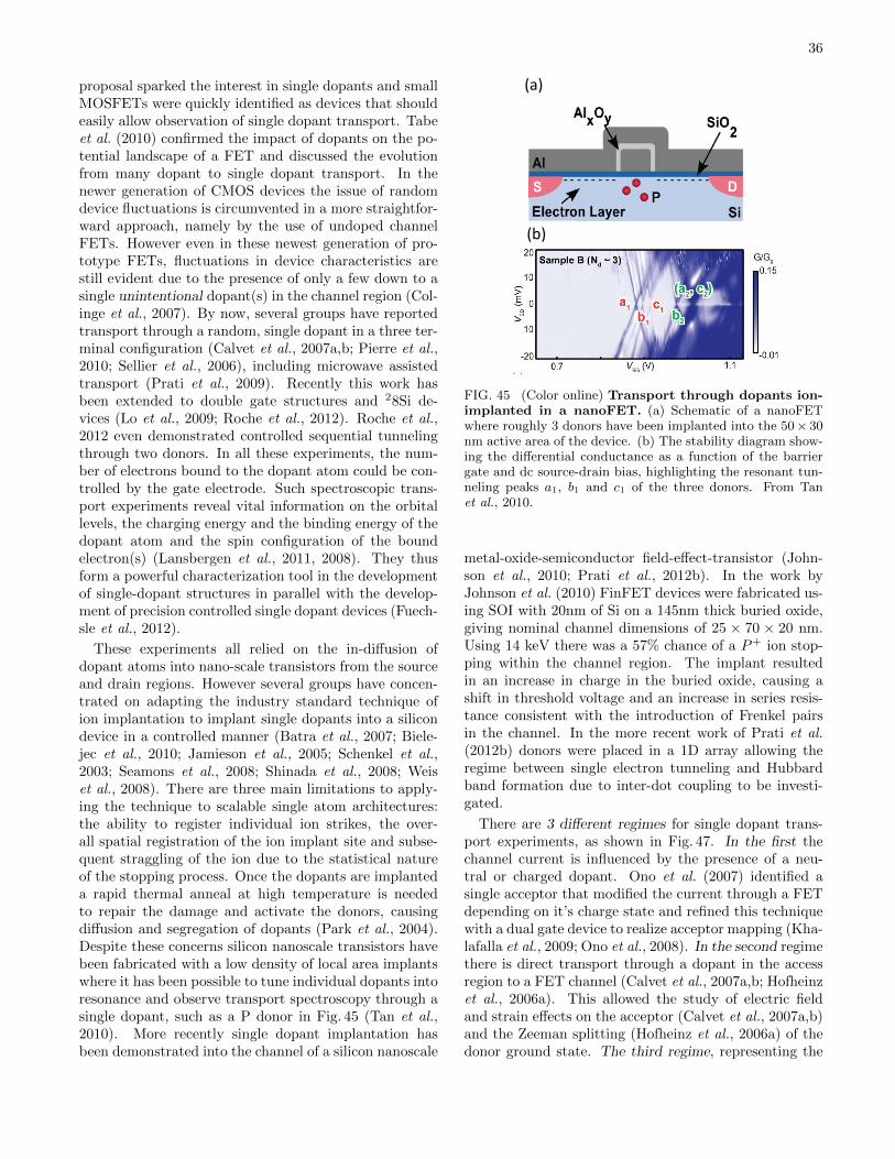
the single-dopant regime as sketched in the third columnhas been reached by several groups. Depending on thearchitecture, the source and drain reservoirs can bemade up of highly-doped Si (Fuechsle et al., 2012; Pierreet al., 2010; Sellier et al., 2006), or of a two-dimensionalelectron gas (Tan et al., 2010). The same goes for thegates, but they can also be metallic (Tan et al., 2010).The resulting single-electron transistors consist of asteep dopant potential well connected to source anddrain reservoirs.
0D structuresLike dopants, self-assembled nanocrystals provide con-finement to zero dimensions, but the confinement isbetter described by a hard-wall potential well in x, y
and z-directions and is much wider (Fig. 1). The energylevels of an electron in a quantum well of size L arequantized according to basic quantum mechanics, seefor example Cohen-Tannoudji et al. (1992). The corre-sponding level spacing ∆E is on the order of h2/meffL
2,where meff is the electron effective mass. The separationbetween energy levels thus decreases quadratically withthe well width: as a result, the discrete levels of e.g.a 30 nm size nanocrystal are expected to have energyspacings 2 orders of magnitude smaller than those of adopant with a 3 nm Bohr radius. Making source anddrain contacts requires very precise alignment by meansof electron-beam lithography. The tunnel couplingof these devices relies on statistics; creating tunabletunnel coupling to self-assembled dots is very challeng-
5
ing. A highly-doped substrate can be used as a globalbackgate and metallic leads on a dielectric as a local gate.
1D structuresThe high aspect ratio of nanowires (NWs) implies a largelevel spacing in the transverse directions, and a smalllevel spacing in the longitudinal direction (Lx � Ly,z),creating a (quasi) 1-dimensional channel with fewsubbands in the transverse direction (see second rowof Fig. 1). Within this channel a zero-dimensional wellcan be created by local gates on the nanowire, or bySchottky tunnel barriers to source and drain contacts.In the latter case the barrier height is determined by thematerial work functions and hardly tuneable in-situ —the tunnel coupling will generally decrease as electronsleave the well and the wave function overlap with sourceand drain shrinks. Local gates, however, can tune thetunnel barriers since the applied gate voltage induces anelectric field which locally pulls up the conduction band.Electrons tunnel from the quantum well into reservoirswhich are part of the nanowire itself. The metallicleads connecting the nanowire to the macroscopic worldmust be ohmic; i.e., the contacts should have hightransparency, to prevent the formation of multiplequantum dots in series (particularly if the contacts arevery close to the quantum dot).
2D structuresA 2-dimensional electron gas (2DEG) can be created inSi MOSFETs (Metal-Oxide-Semiconductor Field EffectTransistors) and in Si/SiGe heterostructures. Electronsare unconfined in the x-y-plane and are confined by atriangular potential well perpendicular to the plane, assketched in in Fig. 1. More realistic band diagrams aredrawn in Fig. 2 in the review by Ando et al. (1982) forSi MOS and Fig. 11 in the review by Schaffler (1997)for Si/SiGe heterostructures. In a 2DEG-based quantumdot, the lateral confinement is a soft-wall potential de-fined by top gate electrodes, enabling tunnel-coupling tosource and drain reservoirs in the 2DEG. Those reservoirsare connected to macroscopic wires via ohmic contacts,which are often highly doped regions at the edge of thechip. The resulting potential landscape is highly tunablethanks to local electrostatic gating via the top gates.
B. Transport regimes
Having introduced quantum-confined devices, we nowcover the basics of quantum transport through single-electron transistors (SETs), which are made up of a zero-dimensional island, source and drain reservoirs, and gateelectrodes.
Electronic measurements on single electrons require aconfining potential which is tunnel coupled to electronreservoirs in source and drain leads, see Fig. 2. The
DS
D
EF
DS
L
DS
EF
S
ΔE
EC+ΔE
Eadd
µS
EC+ΔE
µD
DS
µS µD
µ(N+2)µ(N+2)
(a) (b)
µN
µN+1
µN‐1
µN
µN+1
µN‐1
FIG. 2 (Color online) Schematic diagrams of the elec-trochemical potential of a single-electron transistor.(a) There is no available level in the bias window between µS
and µD, the electrochemical potentials of the source and thedrain, so the electron number is fixed at N due to Coulombblockade. (b) The µN level aligns with source and drain elec-trochemical potentials, and the number of electrons alternatesbetween N and N −1, resulting in a single-electron tunnelingcurrent.
SET-island is also coupled capacitively to one or moregate electrodes, which can be used to tune the electro-static potential of the well. The discrete levels are spacedby the addition energy Eadd(N) = EC + ∆E, which con-sists of a purely electrostatic part, the charging energyEC , plus the energy spacing between two discrete quan-tum levels, ∆E. ∆E is zero when two consecutive elec-trons are added to the same spin-degenerate level. Thecharging energy EC = e2/2C, where C is the sum of allcapacitances to the SET-island1.
In the limit of low temperature, if we only consider se-quential tunneling processes, energy conservation needsto be satisfied for transport to occur. The electrochem-ical potential µN is the energy required for adding theNth electron to the island. Electrons can only tunnelthrough the SET when µN falls within the bias window(see Fig. 2(b)), i.e. when µS ≥ µN ≥ µD. Here µSand µD are the electrochemical potential of the sourceand the drain respectively. Current cannot flow withoutan available level in the bias window, and the device isin Coulomb blockade, see Fig. 2(a). A gate voltage canshift the whole ladder of electrochemical potential levelsup or down, and thus switch the device from Coulombblockade to single-electron tunneling mode. By sweep-ing the gate voltage and measuring the conductance, oneobtains Coulomb peaks as shown in Fig. 3(a).
Usually, one measures the conductance versus source-drain voltage VSD and gate voltage VG in a bias spec-troscopy, as shown in Fig. 3(b). Inside the diamond-shaped regions, the current is blocked and the number ofelectrons is constant. At the edges of these Coulomb dia-monds a level is resonant with either source or drain and
1 We refer to other review articles on quantum dots and single-electron transistors for more background and details: Beenakkerand van Houten (1991); Grabert et al. (1993); Hanson et al.(2007); Kouwenhoven et al. (2001, 1997a); Reimann and Manni-nen (2002); and Van der Wiel et al. (2003)
6
(b)
KondoFWHM~TK
hΓEC
ΔE
eVSD N
Co‐tunneling
eVG
N‐1 N+1
T=0
N‐1 N N+1
G(S)
eVSD=0
hΓ hΓ
hΓ>T>>TK
T << TK(a)
h4e2
h4e2
FIG. 3 (Color online) Zero-bias and finite-bias spec-troscopy. (a) Zero-bias conductance G of transport versusgate voltage VG both at T � TK (solid line) and T � TK
(dashed line). In the first regime, the full width at halfmaximum (FWHM) of the Coulomb peaks corresponds tothe level broadening hΓ. In the Kondo regime (T � TK),Coulomb blockade is overcome by coherent second-order tun-neling processes (see main text). (b) Stability diagram show-ing Coulomb diamonds in differential conductance, dI/dVSD,versus eVSD and eVG at T = 0K. The edges of the diamond-shaped regions (red) correspond to the onset of current. Di-agonal lines of increased conductance emanating from thediamonds (gray) indicate transport through excited states.The indicated internal energy scales EC , ∆E, hΓ and TK de-fine the boundaries between different transport regimes. Co-tunneling lines can appear when the applied bias exceeds ∆E(see main text). Adapted from Lansbergen, 2010.
single-electron tunneling occurs. When an excited stateenters the bias window a line of increased conductancecan appear parallel to the diamond edges. These resonanttunneling features have other possible physical origins, asdescribed in detail by Escott et al. (2010). From such abias spectroscopy one can read off the excited-states andthe charging energy directly, as indicated in Fig. 3(b).
The simple model described above explains success-fully how quantization of charge and energy leads to ef-fects like Coulomb blockade and Coulomb oscillations.Nevertheless, it is too simplified in many respects. Upuntil now we only worried about the electronic proper-ties of the localized state but not about the physics ofthe electron transport through that state. In this sec-tion, based on Lansbergen, 2010, we will describe the fivedifferent regimes of electron transport through a local-ized stated in a three-terminal-geometry. How electronstraverse a quantum device is strongly dependent on thecoherence during the tunneling process and thus dependsstrongly on eVSD and kBT . These external energy scales
should be compared to the internal energy scales of thetunneling geometry that determine the transport regime,namely the charging energy EC , the level spacing ∆E,the level broadening hΓ and the Kondo temperature TK .Here, Γ is the total tunnel rate to the localized statewhich can be separated into the tunnel coupling to thesource electrode ΓS and to the drain electrode ΓD, i.e.Γ = ΓS + ΓD. The internal energy scales are all fixed bythe confinement potential, and the external energy scalesreflect the external environment, namely the temperatureT and the applied bias VSD.
Much literature describes the electronic transport inall possible proportionalities of these energy scales witheach other (Alhassid, 2000; Beenakker, 1991; Buttiker,1988). The internal energy scales are typically related toeach other by TK � hΓ � ∆E � EC , and occasion-ally by TK � ∆E < hΓ � EC , limiting the numberof separate transport regimes that we need to consider.Fig. 4(a) is a schematic depiction of transport regimes asa function of eVSD and kBT . It should be noted thatthe boundaries between transport regimes are typicallynot abrupt transitions. For clarity, internal and exter-nal energy scales (except TK and hΓ) are indicated in aschematic representation of our geometry, see Fig. 4(b).
Here, we will not make a distinction between the ex-ternal energy scales kBT and eVSD when we comparethem to internal energy scales, as indicated by Fig. 4(a).The reason behind this equality is that both these exter-nal energy scales have a very similar effect on the trans-port characteristics. Their only relevant effect is thatthey introduce (hot) phonons to the crystal lattice, ei-ther directly by temperature or by inelastic tunnelingprocesses induced by the non-equilibrium Fermi energiesof the source/drain contacts.
Next, we will describe the five separate tunnelingregimes and their corresponding expressions for thesource/drain current I shortly. These regimes are the so-called multi-electron regime, the sequential multi-levelregime, the sequential single level regime, the coherentregime and the Kondo regime, see Fig. 4(a).
1. The multi-electron regime
Firstly there is the multi-electron regime (EC �kBT, eVSD) where Coulomb blockade does not occur, asmentioned in the start of this chapter. This regime is notrelevant for this review.
2. The sequential multi-level regime
At ∆E � kBT, eVSD � EC the system is in the se-quential multi-level regime. The transport is given by
7
(a)
(b)
S
ΔE
eVSD
D
µD
µN
µN+1
µS
EC
~kBT
kBTK hΓ
kBTK
hΓ
EC
ΔE
eVSD(J)
kBT (J)ECΔE
~kBT
FIG. 4 (Color online) The five separate transportregimes in a three-terminal quantum device. (a)Schematic depiction of the regimes in which transport througha localized takes place as a function of the external energyscales kBT and VSD. The transitions between regimes takeplace on the order of the internal energy scales EC , ∆E, hΓand TK . (b) Potential landscape of the three terminal ge-ometry, where the quantum states and the electrochemicalpotential of the leads are shown together with kBT , VSD andEC , ∆E.
(Beenakker, 1991; Van der Vaart et al., 1993)
I = e
(Γ1
in + Γ2in + ...+ Γnin
)Γ1
out
Γ1in + Γ2
in + ...+ Γnin + Γ1out
, (1)
where the subscript denotes the direction of transport,into or out of the localized state, and the superscript in-dicates the level, where 1 refers to the ground state and nindicates the highest orbital within the energy window setby eVSD. The current thus depends on the ingoing ratesof all levels in the bias window and the outgoing rate ofonly the ground state. Physically, electrons can enter anyorbital state that is energetically allowed. Once a singleelectron is transferred to the localized state, Coulombblockade prevents another electron from entering. Fordopants, the bound electron will relax back to the groundstate before it has a chance to tunnel out of the localizedstate, since the orbital relaxation times (∼ps-ns (Lans-bergen et al., 2011)) are typically much faster than theoutgoing tunnel rates (∼1 ns). For quantum dots thephysics is similar but tunnel rates and orbital relaxationrates are slower, e.g. ∼ 1-10ns‘in GaAs quantum dots(Fujisawa et al., 1998). The inelastic nature of the re-
laxation prohibits coherent transfer of electrons from thesource to the drain electrode.
3. The sequential single-level regime
The next transport regime is the sequential single-levelregime, roughly bounded by hΓ � kBT, eVSD � ∆E,where only a single level resides inside the bias window.This regime is a transition between phase-coherent andphase-incoherent transport between source- and drain-electrodes and the tunneling current depends vitallyon kBT . For VSD = 0 the conductance is given by(Beenakker, 1991)
G =e2
4kBT
Γ1inΓ1
out
Γ1in + Γ1
out
, (2)
where Γin is the tunnel rate into the localized state andΓout is the tunnel rate out. Note that Γin = ΓS ,Γout =ΓD for VSD > 0 and Γin = ΓD,Γout = ΓS for VSD < 0.
If the localized state is strongly coupled to the contactshigher-order transport processes become apparent in theCoulomb blocked region, i.e. the so called co-tunnelinglines indicated in Fig. 3(b). This is the case when EC/Γapproaches unity in the open regime. There is an elasticand inelastic component to the co-tunneling (Averin andNazarov, 1990; Nazarov and Blanter, 2009). The elasticcomponent leads to a constant background current in theCoulomb diamond. The inelastic component leads to astep in the current when the applied bias exceeds ∆E.The current is given by
Iel =ρ2e2
8π2hΓinΓout
1
∆E, (3)
Iin =ρ2e2
6hΓinΓout
(kBT
Ee+kBT
Eh
), (4)
for the elastic and inelastic co-tunneling respectively withEe+Eh = EC , where the energies Ee and Eh denote thedistance to the Fermi energy of the filled and empty stateand ρ is the density of states. The complex co-tunnelingline shape is discussed in depth in Wegewijs and Nazarov,2001.
4. The coherent regime
As soon as the external energy scales are much smallerthen hΓ (TK � kBT, eVSD � hΓ � ∆E) the system isin the coherent regime, where the conductance is givenby Buttiker (1988)
G =e2
~Γ1
inΓ1out
(Γ1in + Γ1
out)2 (5)
8
The conductance is thus given by the quantum conduc-tance e2/~ multiplied by a factor that only depends onthe symmetry between ΓS and ΓD. It has been proven ex-plicitly that this expression, easily derived for resonancesin 1D double barrier structures (Ricco and Azbel, 1984),also holds in three dimensions (Kalmeyer and Laughlin,1987).
5. The Kondo regime
The final transport regime occurs when eVSD, kBT �TK . The Kondo temperature is the energy scale be-low which second-order charge transitions other than co-tunneling start to play a role in the transport (Meir andWingreen, 1993). In first-order transitions, the trans-ferred electrons make a direct transition from their initialto their final state. It should be noted that the constantinteraction model only considers first-order charge tran-sitions (Kouwenhoven et al., 1997a). In a second-ordertransition, the transferred electron goes from the initialto the final state via a virtual state of the atom or dot. Avirtual state is an electronic state for which the numberoperator does not commute with the Hamiltonian of thesystem and therefore has a finite lifetime. The lifetime ofthe virtual state is related to the Heisenberg uncertaintyprinciple, as the electron can only reside on the virtualstate on a timescale t ∼ ~/ (µN − µS,D), where µN−µS,Dis the energy difference between the virtual state and thenearest real state. The main characteristic of this trans-port regime is a zero-bias resonance inside the Coulombdiamond for N=odd, as we will explain next, see alsoFig. 3(a) and (b).
When N = even, the total localized spin is zero due tothe (typical) even-odd filling of the (spin) states, result-ing in zero localized magnetic moment. When N = odd,one electron is unpaired, giving the localized state a netmagnetic moment. In contrast to metals doped withmagnetic impurities, the conductance of double barrierstructures actually increases due the Kondo effect. Thisis because the density of states in the channel at a µS , µD(associated with the newly formed Kondo singlet state)acts as a transport channel for electrons, as if it werea “regular” localized state in the channel. The Kondotemperature can be expressed as (Glazman and Pustil-nik, 2003)
TK =√ECΓ exp(−πµN − µS,D
2Γ) (6)
assuming µN − µS,D � µN−1 − µS,D. The zero-biasKondo resonance is furthermore characterized by its tem-perature and magnetic field dependence. The conduc-tance of the Kondo resonance has a logarithmic temper-ature dependence, which is described by the phenomeno-
logical relationship (Goldhaber-Gordon et al., 1998)
G(T ) = (G)0
(T
′2K
T 2 + T′2K
)s(7)
where T′
K = TK/√
21/s − 1, G0 is the zero-temperatureKondo conductance and s is a constant found to be equalto 0.22 (Goldhaber-Gordon et al., 1998).
III. PHYSICS OF SI NANOSTRUCTURES
Here we describe the fundamental physical propertiesof Si nanostructures. Some of these arise from the elec-tron confinement into a small region (tens of nanometersor less) and are similar to those of other semiconduc-tors, but other properties are present only in Si. Oneexample arises because Si has multiple degenerate val-leys in its conduction band, described in the first section.The valleys play an important role in both dopant andquantum dot devices, although the details of the valleyphysics in those two systems are different. Moreover, inheterostructures, strain often plays an important role,and the interplay between strain, disorder, and the prop-erties of the valleys are important in determining thelow-energy properties of the devices.
A. Bulk silicon: valley degeneracy
Because silicon is used in many technical applications,methods for manufacturing extremely high purity sam-ples are well-developed. Silicon has several stable nuclearisotopes, with 28Si, which has no nuclear spin, being themost abundant (its abundance in natural silicon is 92%).This availability of a spin-zero silicon isotope is usefulfor applications in which one wishes to preserve the co-herence of electron spins, since the absence of hyperfineinteraction eliminates a possible decoherence channel forthe electron spin, see section VI.A.4.
The properties of electrons in silicon have been stud-ied in great detail for many decades (Cohen and Che-likowsky, 1988; Yu and Cardona, 2001). Here we reviewaspects of the material that will prove critical in under-standing the challenges that arise as one works to createdevices with desired properties on the nanoscale. Onesuch aspect is how the effects of multiple valleys presentin the conduction band in bulk silicon appear in specificsilicon nanodevices. The manifestations of valley physicsin quantum dots are different from those in dopant-baseddevices, and understanding the relevant effects is criticalfor manipulating the spin degrees of freedom of the elec-trons in nanodevices. In the following subsections, wefirst define and discuss the conduction band valleys inbulk silicon, and then the behavior and consequences ofvalley physics for quantum dots and for dopant devices.
9
(a) (b)
FIG. 5 Silicon crystal in real and reciprocal space. (a)3D plot of the unit cell of the bulk silicon crystal in real space,showing the diamond or Face-Centered Cubic lattice, whichhas cubic symmetry. (b) Silicon crystal in reciprocal space.Brillouin zone of the silicon crystal lattice. It is the Wigner-Seitz cell of the Body-Centered Cubic lattice. Γ is the centerof the polyhedron. Figure from Davies (1998).
(a) (b)
Gap EG
k
E
Light holes
Heavy holes
Split‐off band
Energy (eV)
ΔSO
XΓL
k0k
0
Conduction band minimum x6
FIG. 6 (Color online) Band structure of bulk silicon. (a)The conduction band has six degenerate minima or valleys at0.85k0. Results kindly supplied by G.P. Srivastava, Universityof Exeter. Figure from Davies (1998). (b) Zoom-in on thebottom of the conduction band and the top of the valenceband (schematic, not exact). The bandgap in bulk Si is 1.12eV at room temperature, increasing to 1.17 eV at 4 K (Green,1990). The heavy and light hole bands are degenerate for k =0. The split-off band is separated from the other subbands bythe spin-orbit splitting ∆so of 44 meV.
Crystalline silicon is a covalently bonded crystal with adiamond lattice structure, as shown in Fig. 5. The bandstructure of bulk silicon (Phillips, 1962), shown in Fig. 6,has the property that the energies of electron states inthe conduction band is not minimized when the crystalmomentum k = 0, but rather at a nonzero value, k0,that is 85% of the way to the Brillouin zone boundary,as shown in Fig. 6(b). Bulk silicon has cubic symmetry,and there are six equivalent minima. Thus we say thatbulk silicon has six degenerate valleys in its conductionband.
In conventional electronic devices, the presence of mul-tiple valleys typically does not affect transport proper-ties in a profound way. However, valley physics plays acritical role in quantum electronics because of interfer-ence between different valleys that arises when the elec-
6‐fold degenerate
E
CB minimum 4‐fold
2‐fold
Bulk 2D
6‐fold degenerate
CB minimum
Bulk 0D
1s(A1)1‐fold
1s (E)2‐fold
1s (T2)3‐fold
E
Valley Splitting
Δ
(a) (b)
EV
Quantum dots DopantsValley Splitting
ΓValley Splitting
FIG. 7 (Color online) Valley splitting of of dopants andof quantum dots in silicon quantum wells. (a) For aquantum well, in which a thin silicon layer is sandwiched be-tween two layers of SixGe1−x, with x typically ∼ 0.25 − 0.3,the six-fold valley degeneracy of bulk silicon is broken by thelarge in-plane tensile strain in the quantum well so that twoΓ-levels are about 200 meV below the four ∆-levels (Schaffleret al., 1992). The remaining two-fold degeneracy is broken bythe confinement in the quantum well and by electric fields,with the resulting valley splitting typically ∼ 0.1− 1 meV.(b) For phosphorus dopants, strong central-cell correctionsnear the dopant break the six-fold valley degeneracy of bulksilicon so that the lowest-energy valley state is non-degenerate(except for spin degeneracy), lowered by an energy 11.7 meV.The degeneracies of higher-energy levels are broken by latticestrain and by electric fields.
tronic transport is fundamentally quantum. For example,the presence of an additional valley greatly complicatesspin manipulation because it can lift Pauli spin block-ade, which is fundamental for many strategies for spinmanipulation in quantum dot nanodevices (Huttel et al.,2003; Johnson et al., 2005a; Koppens et al., 2005; Onoet al., 2002; Rokhinson et al., 2001). In pure bulk sili-con, the valleys are degenerate (the energies of the sixstates related by the cubic symmetry are the same), butin nanodevices this degeneracy can be and usually is bro-ken by various effects that include strain, confinement,and electric fields. When valley degeneracy is lifted, atlow temperatures the carriers populate only the lowest-energy valley state, thus eliminating some of the quantumeffects that arise when the valleys are degenerate.
Fig. 7 shows a summary of valley splitting in het-erostructures and in dopant devices. For strained siliconquantum wells, the large in-plane strain lifts the energiesof the in-plane (x and y) valleys. The remaining two-fold degeneracy of the z-valleys is broken by electronicz-confinement induced by electric fields and by the quan-tum well itself, resulting in a valley splitting of order0.1− 1 meV. The breaking of the two-fold valley degen-eracy is very sensitive to atomic-scale details of the in-terface, and is discussed in detail in Sec. III.B and in thesupplemental material.
For an electron bound to a dopant in silicon, the valleydegeneracy of bulk silicon is lifted because of the strongconfinement potential from the dopant atom (Kohn andLuttinger, 1955a). For phosphorus donors in silicon, the
10
electronic ground state is non-degenerate, with an energygap of ∼ 11.7 meV between the non-degenerate groundstate and the excited states (Andresen et al., 2009; Ram-das and Rodriguez, 1981). Thus, additional degeneracyof the electronic ground state is not a concern in dopantdevices. However, the fact that the conduction band min-imum in silicon is at a large crystal momentum k0 thatis near the zone boundary gives rise to other physical ef-fects that are important for quantum electronic devices.One such consequence arises because the wave functionsof the electronic states in dopants oscillate in space onthe very short length scale ∼ 2π/k0, which is roughlyon the scale of one nanometer. These charge oscillationsdiffer from the electron charge variations due to Bloch os-cillations because they can cause the exchange couplingto change sign, and thus have significant implications forthe design of quantum electronic devices, as discussed inSection III.C.
B. Quantum wells and dots
In the quantum well devices we discuss here, one startswith a material with a two-dimensional electron gas(2DEG), and then lithographically patterns top gates towhich voltages are applied that deplete the 2DEG sur-rounding the quantum dot. By carefully adjusting thegate voltages, one can achieve dots with occupancy ofa single electron, see section IV.D. Moreover, the samegate voltages that are used to define the dot are alsoused to perform the manipulations required for initial-ization, gate operations, and readout of charge and spinstates (Maune et al., 2012), see section VI.C.4.
1. Valley splitting in quantum dots
Understanding the valley degrees of freedom is impor-tant for ensuring that the valley splitting is in a regimesuitable for spin-based quantum computation. Even inthe low-density limit appropriate to single-electron quan-tum dots, where electron-electron interactions (Andoet al., 1982) are unimportant, valley splitting is complex:the breaking of the valley degeneracy involves physics onthe atomic scale, orders of magnitude smaller than thequantum dot itself, so it depends on the detailed prop-erties of alloy and interface disorder. Because the loca-tions of the individual atoms in a given device are notknown, statistical approaches to atomistic device mod-eling or averaging theories like effective mass must beutilized. Theory, modeling, and simulation provide in-sight into the physical mechanisms giving rise to valleysplitting, so that device design and fabrication methodscan be developed to yield dots with valley splitting com-patible with use in spin-based quantum information pro-cessing devices.
In bulk silicon, there are six degenerate conductionband minima in the Brillouin zone (valleys) as depictedin Fig. 5. One modern strategy for fabricating Si de-vices for quantum electronics applications is to use a bi-axially strained thin film of Si grown on a pseudomor-phic SixGe1−x substrate. In such devices, the siliconquantum well is under large tensile strain, and the six-fold degeneracy is broken into a two-fold one (Schaffler,1997). Confinement of electrons in the z-direction in a 2-dimensional electron gas lifts the remaining two-fold val-ley degeneracy, resulting in four ∆-valleys with a heavyeffective mass parallel to the interface at an energy sev-eral tens of meV above the two Γ-valleys (Ando et al.,1982), as shown in Fig. 7. The sharp and flat interfaceproduces a potential step in the z-direction and can liftthe degeneracy of the Γ-valleys in two levels separatedby the valley splitting EV . Built-in or externally appliedelectric fields break the symmetry of the Hamiltonian andcan couple the various valleys and thus lift the valley de-generacy. Theoretical predictions for the valley splittingof flat interfaces are generally on the order of 0.1–0.3meV (Boykin et al., 2004b; Culcer et al., 2010a; Ohkawaand Uemura, 1977; Saraiva et al., 2011). Experimen-tal values in Si inversion layers mostly vary from 0.3–1.2meV, but some are substantially smaller (Koester et al.,1997; Kohler and Roos, 1979; Lai et al., 2006; Nicholaset al., 1980; Pudalov et al., 1985; Weitz et al., 1996). Agiant valley splitting of 23 meV measured in a similarstructure (Takashina et al., 2006) is still not completelyunderstood theoretically (Saraiva et al., 2011).
The two main approaches for understanding valleysplitting in silicon heterostructures are tight-binding cal-culations (Boykin et al., 2007, 2004a, 2005; Kharcheet al., 2007; Srinivasan et al., 2008) and theories thatuse an effective mass formalism (Friesen et al., 2007b;Friesen and Coppersmith, 2010; Saraiva et al., 2009).Section I in the supplemental material reviews a sim-ple one-dimensional tight-binding model (Boykin et al.,2004b) that illustrates some of the physical mechanismsthat lead the breaking of the valley degeneracy and hencethe emergence of valley splitting. A pictorial sketch ofthe two lowest-energy eigenstates of this one-dimensionalmodel is presented in Fig. 8. The eigenfunctions havevery similar envelopes and fast oscillations with a periodvery close to 2π/k0, where k0 is the wavevector of the con-duction band valley minimum. The different alignmentsof the phases of the fast oscillations with sharp interfacescause the energies of the two states to be different, thusgiving rise to valley splitting.
Valley splitting has a complicated dependence on envi-ronmental and structural conditions. Large-scale atom-istic tight-binding calculations can incorporate realisticinhomogeneity in the atomic arrangement, both in termsof alloy disorder and in terms of disorder in the loca-tions of interface steps, as discussed in section III of thesupplemental material. Technically well controlled inter-
11
lowest energy symmetric eigenstate
lowest energy antisymmetric
eigenstate
envelopes of two eigenstates are the same; phases of fast oscillations
are different
wavefunction amplitude
z
quantum well
FIG. 8 (Color online) Sketch of the two lowest energyeigenstates in an infinite square well of the two-bandmodel presented in the supplemental material. Theenvelopes of the two eigenfunctions are very similar to eachother and to the sine behavior obtained in the absence of val-ley degeneracy; the effects of the valley degeneracy give riseto fast oscillations within this envelope. For a square well,one eigenfunction is symmetric and the other is antisymmet-ric; the symmetries are different because the fast oscillationshave different phases, as measured from the quantum wellboundaries. This sensitive dependence of valley splitting onthe atomic-scale physics near the well boundary is the sourceof the sensitive dependence of the valley splitting on disorderat the quantum well interfaces.
faces in Si are buffers of either SiO2 or SixGe1−x, whichare intrinsically atomistically disordered. Some of theeffects of this disorder can be understood qualitativelyusing effective mass theory, but because of the impor-tance of atomic-scale physics in determining valley split-ting, atom-scale theory is required for quantitative un-derstanding. For SixGe1−x, there are 3 critical disordereffects to consider: atom-type disorder, atom-positiondisorder, alloy concentration disorder. A detailed discus-sion of the characterization of the effects of these differenttypes is presented in section III of the supplemental ma-terial.
Many features of the physics that give rise to val-ley splitting can be understood qualitatively and semi-quantitatively using effective mass theories (Kohn andLuttinger, 1955b; Seitz and Turnbull, 1957), if these the-ories are formulated carefully to incorporate the micro-scopic effects that give rise to valley splitting (Friesen,2005; Friesen et al., 2007b; Fritzsche, 1962; Nestoklonet al., 2006; Pantelides, 1978). In the envelope func-tion or effective mass formalism, the theory is writtenin terms of an envelope function for the wave function,which is well-suited for describing variations on relativelylong scales (such as the quantum dot confinement). Theeffects of the degenerate valleys are incorporated using avalley coupling parameter that is treated as a delta func-tion whose strength is determined by the atomic scale
physics (Chutia et al., 2008; Friesen et al., 2007b; Saraivaet al., 2009). The envelope function formalism has theadvantage that one can obtain analytic results for valleysplitting in nontrivial geometries (Culcer et al., 2010a,b;Friesen et al., 2007b; Friesen and Coppersmith, 2010).However, the theory must explicitly incorporate infor-mation from the atomic scale, either as a valley couplingparameter that is fit to tight-binding results, as the out-put of a multiscale approach (Chutia et al., 2008; Saraivaet al., 2009), or by explicit atomistic calculation on largescales, as embodied by the NEMO tool suite (Boykinet al., 2004b; Klimeck et al., 2007, 2002; Steiger et al.,2011). More details of effective mass theory treatment ofvalley splitting are in the supplemental material.
2. Mixing of valleys and orbits
When the valley splitting EV is much greater than theorbital level spacing ∆E, electrons will occupy single-particle levels with orbital numbers 1, 2, 3, ... and val-ley number V 1, the lowest valley state (see Fig. 9(a)).Conversely, if ∆E � EV the first four electrons willoccupy the valleys V 1 and V 2 in the lowest orbit be-fore going to the next orbit with n = 2, as shown inFig. 9(b). However, valleys and orbits can also hybridize(Friesen and Coppersmith, 2010), making it inappropri-ate to define distinct orbital and valley quantum num-bers (see Fig. 9(c)). Depending on the degree of mixing,the valley-orbit levels V O1, V O2 etc, behave mostly likevalleys or like orbits. Instead of referring to a pure val-ley splitting EV the term valley-orbit splitting is used,EV O = EV O2 − EV O1 for the difference in energy be-tween the first two single-particle levels, EV O1 and EV O2.This is referred to as the ground-state gap (Friesen andCoppersmith, 2010).
The behavior of the valley splitting in real quantumwells is complicated by the fact that in real devices thequantum well interface is not perfectly smooth and ori-ented perpendicular to z. The energy difference betweenthe two lowest eigenstates depends on the relationshipbetween the phase of the fast oscillations of the wavefunction with the heterostructure boundary, and a stepin the interface alters this phase relationship. The low-est energy wave function minimizes the energy, and, asshown in Fig. 8, can cause the phase of the fast oscilla-tions to become dependent on the transverse coordinatesx and y. This coupling between the z-behavior and thex-y behavior is called valley-orbit coupling.
As discussed in subsection III.B.1 above, in a siliconquantum well under tensile strain, there are two low-lying conduction band valleys at wavevectors +k0z and−k0z, whose energies are split by the effects of confine-ment potentials and electric fields perpendicular to z.In the limit of a perfectly smooth interface aligned per-pendicular to z, the valley splitting of a quantum well
12
EVO
E
Orbitals
(a) (b)
EV
(a) EV >> ΔE: no mixing
Valleys
EV << ΔE
V1V2
n=1
n=2
ΔE
n=3
(b) EV << ΔE: no mixing
n=1
n=2
ΔE
n=3
V1V2
V1V2
V1V2
Orbital # Valley #
n=1
n=2ΔE
n=3
n=1
n=2n=3
V1
V2
Orbital# Valley #
(c)
EV
(c) EV ≈ ΔE: Mixing of valleys and orbits
V1
Orbital # Valley #
n=1
n=2
n=3 V2
n=4
Valley‐orbit #
VO1
VO2
VO3
VO4
EVO
Valley‐orbits
VO1
VO2
VO3
VO4
EV
EV
ΔE
EV
ΔE
FIG. 9 (Color online) Valley-orbit mixing. (a,b) If thevalley splitting EV and orbital level spacing ∆E have verydifferent values, the orbital and valley quantum numbers arewell-defined and there will be no mixing of orbital and valley-like behavior. (c) When EV≈∆E the valleys and orbits canhybridize in single-particle levels separated by the valley-orbitsplitting EV O.
with typical width and doping is of order 0.1 meV, amagnitude that can be understood using the simple one-dimensional model presented in section I of the supple-mental material.
If the step density of the quantum well interface isreasonably high, then the transverse oscillations of thecharge density cannot align with the entire interface, andvalley splitting is greatly suppressed (Ando, 1979; Friesenet al., 2007b, 2006). The physical picture that emergesfrom effective mass theory that incorporates valley-orbitcoupling is that the envelope function for the wave func-tion in a silicon heterostructure is qualitatively similar totypical wave functions in quantum dots, but that thereare also fast oscillations with wave vector ∼ k0 in thez-direction. The fast oscillations of the two valley stateshave different phases. In the presence of interfacial disor-der such as interfacial steps, the value of the valley phasethat minimizes the energy becomes position-dependent,so that one fixed value of the phase cannot minimize theenergy everywhere, and the energy difference between thetwo different valley states decreases. This suppressionexplains measurements performed in Hall bars (Khrapaiet al., 2003; Koester et al., 1997; Lai et al., 2004; Weitzet al., 1996) that yield very small values for the valleysplitting of only µeV, and also why singlet-triplet split-tings in dots with two electrons have been observed withboth positive and negative values at non-zero magneticfield (Borselli et al., 2011a) — if the electron wave func-
FIG. 10 Valley-orbit coupling from interface steps.Top: gray-scale visualization of wave function oscillations inthe presence of a perfectly smooth interface, oriented perpen-dicular to z. Middle: The relationship between the phase ofthe wave function oscillations and the interface is different onthe two sides of an interface step. When the steps are closetogether, the phase does not adjust to the individual steps,and the valley splitting is suppressed. Bottom: When stepsare far enough apart, the oscillations line up with the interfacelocation on both sides of the steps, which causes the phase ofthe oscillations to depend on the transverse coordinate. Thiscoupling between the behavior of the wave function in the zdirection and in the x− y plane, which arises even when thewell is atomically thin, is known as valley-orbit coupling.
tion straddles a step, then the valley splitting is small,which, together with the effects of electron-electron inter-actions, causes the triplet state to have lower energy thanthe singlet state. If an electron is confined to a regionsmall enough that it does not extend over multiple steps,then the valley splitting is not affected by the steps. Overthe past several years, measurements of valley splittingin quantum point contacts (Goswami et al., 2007) and ofsinglet-triplet splittings in quantum dots (Borselli et al.,2011a,b; Simmons et al., 2011; Thalakulam et al., 2011)in Si/SiGe heterostructures demonstrate that these split-tings can be relatively large, of order 1 meV, when theelectrons are highly confined. These splittings are largeenough that valley excitations are frozen out at the rele-vant temperatures for quantum devices (∼ 100 mK).
There are two different manifestations of valley-orbitcoupling. The first, illustrated in the bottom panel ofFig. 10, occurs when the phase of the valley oscillationsdepends on the transverse coordinate. The second type ofvalley-orbit coupling can be visualized by considering aninterface with a nonuniform step density. A wave func-tion localized in a region with few steps has larger valleysplitting and hence lower energy than a wave functionlocalized in a region with many steps (Shi et al., 2011).Therefore, the presence of the valley degree of freedomleads to translation of the wave function in the x-y plane.Valley-orbit coupling is important when the scale of thevariations of the orbital and valley contributions to the
13
(a) (b)
FIG. 11 A silicon-based nuclear spin quantum com-puter (a) Schematic of Kane’s proposal for a scalable quan-tum computer in silicon using a linear array of 31P donors ina silicon host. J-gates and A-gates control respectively theexchange interaction J and the wave function, as shown in(b). Reproduced from Kane (1998).
energy are similar, a situation that occurs frequently infew-electron quantum dot devices.
Because valley-orbit coupling and valley splitting de-pend on interface details, the observation of valley split-tings that vary substantially between devices (Borselliet al., 2011b) is not unexpected. Understanding and con-trolling this variability is important for being able to scaleup the technology and for the development of devices thatexploit the valley degree of freedom (Culcer et al., 2009a,2012; Li et al., 2010; Shi et al., 2012). Therefore, im-proved understanding of the physical mechanisms thataffect valley splitting in real devices remains an impor-tant topic of active research. The valley-orbit couplingalso contains phase information, which can be used forquantum computation (Wu and Culcer, 2012).
C. Dopants in Si
1. Wave function engineering of single dopant electron states
The central theme of quantum electronics applica-tions using single dopants is the ability to modify thedopant electron wave function using external electricfields and/or to manipulate the spin degrees of freedomusing magnetic fields. In many proposals for dopantbased qubits using either electron or nuclear spins as thequbit states, dopant electron wave function engineeringis critical to effect single and two qubit gates. Since mostwork has been done on n-type dopants, this section willfocus on donors. The original idea comes from the Kaneproposal for a nuclear-spin based quantum computer insilicon (Kane, 2000) where the single qubit operations areimplemented by tuning the contact hyperfine interactionto bring the donor electron into resonance with a trans-verse oscillating magnetic driving field (see Fig. 11). Tosee this we write the effective spin qubit Hamiltonian ofa single donor nucleus-electron system in the presence ofa gate potential with strength V at the donor position as
(a)
(b)
FIG. 12 (Color online) Relative Stark shift of the con-tact hyperfine interaction for different donor depths(z) calculated for a uniform field in the z direction.(a) Using the tight-binding approach (Martins et al., 2004),and (b) Direct diagonalization in momentum space (Wellardand Hollenberg, 2005). Agreement in overall trends is rea-sonable, and for the z = 10.86 nm case both methods predictionization at ∼6 MV/m.
(Goan, 2005; Kane, 1998)
H1Q = µBBzσze − gnµnBzσzn +A(VA)~σn.~σe, (8)
where µB is the Bohr magneton, gn the Lande factor for31P, and µn is the nuclear magneton. The contact hyper-fine interaction strength A can be tuned by an appliedelectric field arising from a bias VA on an A-gate as:
A(VA) =2
3|ψ(0, VA)|2µBgnµnµ0, (9)
where µ0 is the permeability of silicon and ψ(0, VA) isthe donor electron wave-function evaluated at the nucleusunder the A-gate bias VA.
The change in the strength of the contact hyperfinecoupling due to the application of a gate bias has beenstudied by several authors since Kane’s proposal. Todetermine the change in the contact hyperfine couplingstrength it is necessary to calculate the shift in the donorelectron wave function at the position of the donor nu-cleus. Depending on the applied bias polarity, an A-gatecontrol electrode will either draw the wave function to-ward, or away, from the gate. In either scenario the wave
14
function at the donor nuclear position is perturbed tosome extent. The resulting tuning of A depends crit-ically on device parameters such as the depth of thedonor from the interface, and the gate/interface geom-etry. The level of sophistication of the treatment of thedonor electron wave function in these devices has steadilyimproved since the original calculations following Kane(1998). The earliest approaches used fairly simple hy-drogenic wave functions scaled by the dielectric constantof silicon. Larionov et al. (2000) treated the bias poten-tial analytically, and the shift in the hyperfine interactionconstant as a function of applied bias voltage was calcu-lated using perturbation theory. Wellard et al. (2002),again using scaled hydrogenic orbitals treated the prob-lem using a more realistic gate potential (modeled using acommercial semi-conductor software package, with builtin Poisson solver). The donor electron wave function wasexpanded in a basis of hydrogenic orbitals in which theHamiltonian was diagonalized numerically. Kettle et al.(2003) extended these calculations using a basis of non-isotropic scaled hydrogenic orbital states. Smit et al.(2003, 2004) used group theory over the valley manifoldand perturbation theory to describe the Stark shift of thedonor electron while Martins et al. (2005, 2004) appliedtight-binding theory to obtain the first description of theStark shift of orbital states and the hyperfine interactionincorporating Bloch structure. Meanwhile, the effectivemass treatment was further developed in a combined vari-ational approach (Friesen, 2005) and (Calderon et al.,2009), and in (Debernardi et al., 2006) using a Gaussianexpansion of the effective-mass theory (EMT, see sectionII of the supplemental material) envelope functions. Thiswas followed by the application of direct diagonalizationin momentum space (Wellard and Hollenberg, 2005) al-lowing the potential due to the A-gate to be includedat the Hamiltonian level and gave a similar picture ofthe Stark shift of the hyperfine interaction as a functionof external field strength and donor depth as the ear-lier tight-binding treatment of Martins et al. (2004) (seeFig. 12). Although not optimized computationally, themomentum space diagonalization approach has served asa consistency check against larger scale real-space tight-binding calculations of the Stark shift of the donor hy-perfine interaction at low fields (Rahman et al., 2007) inthe overall benchmarking against experiment (Bradburyet al., 2006) which shows the theoretical description hasconverged to a reasonable level in terms of internal con-sistency and comparison with experiment (see Fig. 13). Itshould be noted that in such descriptions encompassingthe overall donor electron wave function it is the relativechange in the contact hyperfine interaction as a functionof electric field that is computed since these approachesdo not describe well the details of the electron state atthe nucleus. Absolute calculations of the contact hyper-fine interaction are the domain of ab-initio theories wherethey have had remarkable success despite the truncation
of the long range part of the donor potential (Gerstmann,2011; Overhof and Gerstmann, 2004).
In more recent years, the effect of depth and proximityto the interface on donor orbital states (Calderon et al.,2008, 2006b; Hao et al., 2009; Rahman et al., 2009a)has received more attention as key experimental mea-surements became available. A turning point was themeasurement of donor orbital states through transport inFinFET devices. The observed donor energy levels werevery different from the bulk spectrum (see section V.C).Extensive tight-binding calculations were used to explorethe space of electric field and donor depth on the quan-tum confinement conditions of the donor-associated elec-tron, identifying Coulombic, interfacial, and hybridizedconfinement regimes. These calculations provided anexcellent description of the low lying donor states ob-served and determination of the donor species (Lansber-gen et al., 2008). It would appear that the theoreticaldescription of electric field “wave function engineering”of the donor electron across device dimensions is nowwell understood. The context of the Kane donor qubithas spurred further refinements of the theoretical descrip-tion of donor states, including the site-specific contactand non-isotropic hyperfine interaction terms (Ivey andMieher, 1975a,b) for wave function mapping under elec-tric fields (Park et al., 2009), interaction with magneticfields and gate control of the g-factor (Rahman et al.,2009b; Thilderkvist et al., 1994), dynamics of moleculardonor-based systems (Hollenberg et al., 2004; Hu et al.,2005; Rahman et al., 2011b; Wellard et al., 2006), cross-talk in hyperfine control (Kandasamy et al., 2006), co-herent single electron transport through chains of ion-ized donor chains (Rahman et al., 2009b), spin-to-chargereadout mechanisms (Fang et al., 2002; Hollenberg et al.,2004), and the calculation of donor levels in the pres-ence of STM-fabricated nanostructures providing modi-fications to the overall potential in a single-atom transis-tor, as shown in section V.B.3 (Fuechsle et al., 2012).
2. Two-donor systems and exchange coupling
In the quantum computing context, the two main ap-proaches to directly couple the spins of donor electronsare through the Coulomb-based exchange interaction be-tween proximate donor electrons, or the magnetic dipoleinteraction. The Kane model uses gate control of theexchange interaction as per the two-qubit effective spinHamiltonian:
H2Q = µBBzσze1 − gnµnBzσ
zn1
+A1(VA1)~σn1.~σe1(10)
+ µBBzσze2 − gnµnBzσ
zn2
+A2(VA2)~σn2.σe2
+ J(VJ)~σe1 .σe2 .
In this equation we apply equation 8 on two dopantsand add the exchange-coupling J between the dopants.There have been a number of papers investigating the
15
Both methods described here are applicable to otherhosts and impurities. To describe other group V impurities,the hydrogenic Coulomb potential is still valid in the bulk,but the core corrections need to be adjusted to reflectcorrect experimental binding energies.
Figure 1 summarizes the effects of the electric field andthe interface on the donor electron. The TB calculationsuse a domain of 32 nm� 65 nm� 32 nm zinc blendelattice with 3:45� 106 atoms. The distance between theimpurity and the interface is varied parallel to the electricfield. The BMB calculation assumes a maximal depth of10.86 nm from the interface and employs a basis set of7986 states. The choice of this depth is dictated by the easeof computation as it is sufficiently deep to nullify surfaceeffects while not too deep to make the problem computa-tionally intractable. In TB, a range of depths from 5 to32 nm have been considered. For each TB data point, thetypical computation times require about 7 hours on20 CPUs [30]. Figure 1(a) shows the variation of �A� ~"�with electric field for various impurity depths. The data arefitted to the quadratic equation of (2). As the depth in-creases, the quadratic coefficient �2 approaches a constantvalue, while the linear coefficient �1 becomes negligible[Fig. 1(b)]. For small impurity depths, �1 is comparable to�2, which results in a shift of the peak of the parabola inFig. 1(a) towards a nonzero electric field. If the linear Starkeffect is negligible, an applied electric field has two effectson the ground state wave function: (i) a decrease in thepeak amplitude of the wave function at the impurity site,reflected by a decrease in A� ~"� in Fig. 1(a) for higher
depths, and (ii) a shift in the mean position of the wavefunction opposite the electric field, giving rise to a nonzerodipole moment as shown in Fig. 1(c). The dipole momentsvary linearly with the electric field, and their slopes ap-proach a constant value as the depth increases [Fig. 1(d)].The wave function plots of Fig. 2 also demonstratethese effects. The larger distortions of the wave functionat higher electric fields explain the increasing dipolemoments.
If the impurity is close to the interface, the wave func-tion is distorted even at zero electric field. This distortioncomes from changes in the slope of the part of the wavefunction between the impurity and the interface. Also themean position of the wave function shifts farther as thedistance between the impurity and the interface is reduced.These effects give rise to an asymmetric charge distribu-tion about the impurity, and a nonzero dipole moment isobserved even at " � 0. This is verified by the shift of the yintercept of the lines in Fig. 1(c) for small impurity depths.In effect, the interface behaves like an electric field pushingthe donor electron away from it. The strength of this fieldincreases as the impurity is placed closer to the interface.This means that a higher electric field directed away fromthe interface is needed to counteract these interface effectsand to restore the decreasing behavior of A� ~"�, as demon-strated in Fig. 1(a).
Some of the numerical results can be explained qualita-tively with the perturbation model using a basis of unper-turbed impurity wave functions f�0
mg, where m indexesincreasing binding energy (m � 0 being the ground state).For an electric field given by q"y, the wave functioncorrected to first order is expressed as
j�10i � j�
00i � q"
X
m�0
X
i
h�0m;ijyj�
00i
E00 � E
0m;i
j�0m;ii; (4)
where i is the degeneracy index for a state m. The dipolemoment D � qh�1
0jyj�10i is then given by
(a)
−5 0 5−6
−5
−4
−3
−2
−1
0
1
x 10
−5
y−y0 (nm)
|ψ(ε
,r)|
2 −|ψ
(0,r
)|2
ε=0.5 MV/mε=1.0 MV/m
(b)
FIG. 2 (color online). (a) Electric field-induced differentialmap of donor electron wave probability density j��"; z0�j
2 �j��0; z0�j
2 shown as a 2D cut through the impurity center at z0 �16:29 nm for " � 0:5 MV=m. The electric field is directed alongthe negative y axis. (b) 1D cut though the center of the impurityparallel to the electric field showing the differential map of theprobability density for two different electric fields.
0 0.2 0.4−8
−6
−4
−2
0
2x
10−4
ε (MV/m)
∆A/A
0 10.86 nm (BMB)
8.14 nm (TB)
10.86 nm (TB)
16.29 nm (TB)
10 20 30−3
−2.5
−2
−1.5
Depth (nm)10 20 30
0
2
4
6
η1
η2
η 2( µ
m2/V
2) x
10-3
η 1( µ
m/V
) x 1
0-3
0 0.2 0.4−8
−4
0
4
ε (MV/m)
21.72 nm
9.23 nm
7.60 nm
5.43 nm
<Ψ
|y−y
0|Ψ
> (n
m)
x10−2
10 20 305
6
7
8
Depth (nm)
d(<
Ψ|y
−y
0| Ψ>
)/d
εx1
0−2
FIG. 1. (a) Electric field response of hyperfine coupling atvarious impurity depths (BMB and TB). (b) Quadratic (left-hand axis) and linear (right-hand axis) Stark coefficients withdepth (TB). (c) Mean position of the ground state electrondistribution (dipole moment) as a function of the electric field(TB). (d) The electric field gradient of the dipole moments [i.e.,the slopes of the lines in (c)] with respect to depth (TB).
PRL 99, 036403 (2007) P H Y S I C A L R E V I E W L E T T E R S week ending20 JULY 2007
036403-3
FIG. 13 Low-field Stark shift of the hyperfine inter-action for momentum space diagonalization (BMB)and tight-binding (TB) methods. (a) Electric field re-sponse of hyperfine coupling at various donor depths (BMBand TB). (b) Quadratic (lefthand axis) and linear (right-handaxis) Stark coefficients as a function of donor depth (TB). (c)Shift of the ground state electron distribution (dipole mo-ment) as a function of the electric field (TB). (d) The electricfield gradient of the dipole moments as a function of donordepth (TB). From Rahman et al. (2007).
construction and fidelity of two-qubit gates (e.g. such asthe controlled-NOT) from this Hamiltonian (Fang et al.,2005; Fowler et al., 2003; Hill and Goan, 2003, 2004; Ker-ridge et al., 2006; Tsai et al., 2009; Tsai and Goan, 2008).From a microscopic physics viewpoint, in general the ex-change energy J is stronger than the dipole interactionfor smaller separations, however it behaves as (Herringand Flicker, 1964)
J(R) ∼ (R/a∗)5/2exp(−2R/a∗), (11)
where R is the donor separation and a∗ is the effectiveBohr radius of the electron wave function. The exchangecoupling dominates over dipole coupling for donors thatare separated by less than approximately 20-30 nm.
The valley degeneracy of the silicon conduction bandgives rise to a far more complicated dependance of J onthe donor separation (so-called “exchange oscillations”)as noted in the early work of Cullis and Marko (Cullisand Marko, 1970), and is particularly relevant in theKane quantum computer context (Koiller and Hu, 2005;Koiller et al., 2002a, 2003) (see Fig. 14). The effectpersisted in effective mass treatments in which the ex-change integrals over Bloch states were carried out nu-merically (Koiller et al., 2004; Wellard et al., 2003). Forsome time these “exchange oscillations” were seen as afundamental limitation of donor based quantum comput-ing as it was thought that to achieve a given exchange
FIG. 14 (Color online) J-oscillations in the exchangecoupling. Calculated exchange coupling between two phos-phorus donors in Si (solid lines) and Ge (dashed lines) alonghigh-symmetry directions for the diamond structure. Valuesappropriate for impurities at substitutional sites are given bythe circles (Si) and diamonds (Ge). Off-lattice displacementsby 10% of the nearest-neighbor distance lead to the perturbedvalues indicated by the squares (Si) and crosses (Ge). Repro-duced from Koiller et al. (2002a).
coupling the donors would have to be placed in the lat-tice with lattice site precision (Koiller et al., 2002a), al-though Koiller et al. (2002b) found that strain could beused to lift the valley degeneracy and alleviate the prob-lem to some extent. In these treatments the exchangecoupling is calculated in the Heitler-London approxima-tion (Calderon et al., 2006a; Koiller et al., 2004) usingeffective mass wave functions containing a single Blochcomponent from each valley minimum, hence it is per-haps not surprising that the overlap integral results inan oscillatory behavior in the donor separation at thelevel of the lattice constant. When the exchange inte-gral is computed using a more accurate wave functionincluding many such Bloch states to reproduce the ob-served donor levels and valley splittings, the interferenceeffect is somewhat smeared out (Wellard and Hollenberg,2005) over the background Herring-Flicker dependence inequation 11 (see Fig. 15). Nonetheless, the issue remainsthat in fabricating donor devices there will be some levelof imprecision in the donor atom placement and hencea variation in the (un-gated) value of J between donorpairs, however, using STM fabrication these errors mightbe constrained to the single lattice site level.
In any case, all components of a quantum computerwill need some form of characterization. For all donorqubit logic gates (single and two qubit), considerationsof background noise sources and decoherence also need tobe taken into account, e.g. see Fowler et al. (2003); Hill
16
FIG. 15 (Color online) Smoothing out the exchangeoscillations - the exchange coupling J as a functionof donor separation along [110]. Top curve: Calcula-tion using the effective-mass wave function. Middle curve:Calculation of J based on wave functions obtained using di-rect momentum diagonalization over a large basis of Blochstates (BMB) with no core-correction of the impurity poten-tial (η = 0). Bottom curve: BMB calculation of J with a core-correction (η = 5.8) that reproduces the donor ground-stateand valley-splitting. Note that the points refer to substitu-tional sites in the silicon matrix. Although the donor separa-tions are relatively small in this case, the spatial variation ofthe exchange interaction appears to be significantly dampedcompared to the effective mass treatment. All J values arecalculated in the Heitler-London approximation. Reproducedfrom Wellard and Hollenberg (2005).
and Goan (2003); Saikin and Fedichkin (2003); Wellardand Hollenberg (2001, 2002) (the decoherence of donorelectron spins is covered in Section VI). Robust controltechniques have been developed specifically for the even-tuality of some level of variation in the exchange coupling(Hill, 2007), which in conjunction with gate characteriza-tion protocols (Cole et al., 2006; Devitt et al., 2006) havethe potential to produce high fidelity two qubit gates inthe Kane scheme (Testolin et al., 2005). Tsai et al. (2009)have applied control techniques to optimize the CNOTgate in the Kane scheme. A more serious impediment toemploying the exchange interaction for quantum gatesis the effect of charge noise (Hu and Das Sarma, 2006;Vorojtsov et al., 2004). Because the exchange interac-tion is ultimately derived from an overlap of electronicwave functions, variations in the background potentialsuch as from charge noise in the device can affect theexchange coupling and may require further developmentof the materials design (Kane, 2005), and/or quantumcontrol techniques.
The control of the exchange interaction J has alsoreceived considerable attention since the original Kanepaper. Early calculations of the dependence of J onan external J-gate bias were carried out by Fang et al.(2002) using a Gaussian expansion (see Fig. 16). Sub-sequent calculations of the J-gate control in various ap-proaches describing the two-electron physics were carried
FIG. 16 Gate control of the two-donor system. Aver-aged charge distribution along the interdonor axis for variousstrengths of the J-gate potential (µ) for the singlet (a) andtriplet (b) states (fixed donor separation at 10 aB). Repro-duced from Fang et al. (2002).
out (Calderon et al., 2007; Fang et al., 2005; Kettle et al.,2006, 2004; Wellard and Hollenberg, 2004) given furtherinsight into the controllability of the exchange interac-tion. However, the gate modification of the overlap be-tween electron states is a difficult calculation and mostlikely a full configuration interaction framework incorpo-rating valley physics and Bloch structure is required toobtain quantitative results to compare with experimentsonce measurements are made. A related problem is thecalculation of the two-electron donor state (D−), notori-ously difficult in the case of a hydrogen ion in vacuum,but even more so when the non-trivial valley physics isadded in to complicate such simple points of referenceas Hund’s Rule. In the context of single donor quantumcomputing Fang et al. (2002) calculated the effect of elec-tric fields on the D− state, which was a key component ofthe spin-to-charge conversion read-out scheme of Kane.In Hollenberg et al. (2004) time-dependent calculations ofthe D0 D0 → D+ D− transition were undertaken in a pro-posal for resonant based spin-to-charge conversion. Morerecent calculations have focussed on the complication ofvalley physics in the D− bound states particularly un-der electric fields (Calderon et al., 2010a; Rahman et al.,2011a), with some notable success in comparisons withrecent experimental measurements (Fuechsle et al., 2012;Lansbergen et al., 2008).
3. Planar donor structures: delta-doped layers and nanowires
The atom-by-atom fabrication of monolayer donorstructures using STM techniques represents the state-of-the-art in precision silicon devices (see section V.B.3).From a theoretical point of view these structures presentnew challenges in order to describe not just their inher-ent physics (band structure, Fermi level, electronic ex-tent, valley splitting, effect of disorder etc), but their useas in-plane gates in quantum electronic devices, includ-ing quantum computing. In understanding the physicsof these highly doped monolayer systems ab-initio tech-
17
niques have been used to good effect. Paradoxically, ab-initio techniques whilst being severely limited to rela-tively small numbers of atoms can handle planar sys-tems with a high degree of symmetry, exploiting peri-odic boundary conditions of the supercell in the planeof the structure with sufficient silicon “cladding” verti-cally for convergence. The earliest calculations in thiscontext were by Qian et al. (2005) for the infinite 2Dplanar (“delta-doped”) ordered layer using a Wannier-based Density Functional Theory (DFT) approach (seeFig. 17(a)). Carter et al. (2009) carried out an exten-sive DFT calculation of the same Si:P structures us-ing a single zeta polarized basis providing a comprehen-sive picture of the band structure, effective potential,Fermi energy and electronic width as a function of pla-nar doping density, finding converged results for claddingabove 80 layers (see Fig. 17(b)). More recently the ef-fect of disorder on the physics of the delta-doped layerhas been investigated both in a DFT approach (Carteret al., 2011, 2009), and in a self-consistent tight-bindingapproach which can handle much larger supercell sizesand hence more accurately represent instances of disor-der (Lee et al., 2011). These calculations indicate thatthe valley spitting of the sub-Fermi bands is quite sensi-tive to the degree of disorder and will play an importantrole in eventual device applications.
The question of convergence between methodologiesstill remains on important quantities such as valley split-ting. Drumm et al. (2012a) have applied distinct DFTapproaches based on localized and de-localized basis setsto calculate the properties of delta-doped layers. Theyobtain convergence in the description of the valley split-ting and Fermi level only when the localized basis set isextended to the double zeta polarized level. The DFTcalculations of the band structure have informed a self-consistent effective mass description of Si:P monolayerstructures (Drumm et al., 2012b), which has been effec-tive in describing states observed in a STM fabricated7-donor planar quantum dot (Fuechsle et al., 2010). Theself-consistent tight-binding approach has also been em-ployed beyond the delta-doped layer to describe recentSTM fabricated devices. In Weber et al. (2012a) theelectronic structure of Si:P monolayer wires only fouratoms wide was calculated and gave results in termsof the number of conduction modes in good agreementwith experiment. The most ambitious calculation to datewas a simulation of the single-atom transistor (Fuechsleet al., 2012) where the same self-consistent tight-bindingapproach was used to determine the effective potentialdue to planar gates at the channel-donor site and subse-quently coupled with a tight-binding description of thedonor electronic levels. The agreement of the calculatedD0 and D− charge transitions with the measurements wasindeed remarkable given the complexity of the device andis a strong indication that the theoretical description ofdonor based quantum electronic devices is well in hand.
(a)
(b)
FIG. 17 Band structure of the 1/4 monolayer phos-phorus δ-doped layer Top: (a) The calculation by Qianet al. (2005): the solid lines show the band structure withoutexchange-correlation and short-range effects, while the dottedlines show the band structure obtained in the full model. (b)The DFT calculation in a supercell with 200 cladding layersby Carter et al. (2009). The plane projected bulk band struc-ture of Si is represented by the gray continuum. The Fermilevel is indicated by a horizontal dashed line. Reproducedfrom Qian et al. (2005) and Carter et al. (2009).
IV. QUANTUM DOTS IN SI AND SIGE
Quantum dots showing Coulomb blockade and display-ing single-electron physics can be created in Si and SiGein many different ways. In this section we first brieflyreview the early work aimed at the demonstration ofCoulomb charging effects in Si and SiGe. An empha-sis in this work was the quest to see Coulomb effectsat as high a temperature as possible. We then discussmodern approaches to quantum dot fabrication. The ap-plication of charge sensing methods is shown to enablea wide range of experiments, including calibration of theabsolute electron number, spin-state spectroscopy, andthe measurement of spin filling as a function of electronnumber. We close this section with a discussion of bothtransport and charge sensing measurements in silicon-based double quantum dots.
A. Early work: Coulomb blockade in silicon
In this section we discuss early experiments studyingCoulomb blockade in Si devices. Additional backgroundand details can be found in Ahmed (1997); Likharev(1999); Meirav and Foxman (1996); Ono et al. (2005);Takahashi et al. (2002); and Tilke et al. (2001).
18
FIG. 18 (Color online) Calculated electronic spectrumof a single-atom transistor. Top left: Calculated energiesof the D0 and D− ground states (GS) as a function of theapplied gate voltage VG. The difference in the energy of thesetwo ground states gives a charging energy of EC ≈ 46.5 meV,which is in excellent agreement with the measurement in thisdevice. Potential profiles between source and drain electrodescalculated for VG = 0.45 V (top middle) and 0.72 V (bottomleft). The calculated orbital probability density of the groundstate for the D0 potential (top right) is more localized aroundthe donor than for the D− potential (bottom right), which isscreened by the bound electron. Reproduced from Fuechsleet al. (2012).
Experiments exploring intentional Coulomb blockadeand transport through Si/SiO2 and Si/SiGe quantumdots dates to the early 1990s, shortly after the discov-ery of Coulomb blockade (Field et al., 1990; Fulton andDolan, 1987; Meirav et al., 1990; Scott-Thomas et al.,1989). The primary requirements for the observationof Coulomb blockade are to isolate a small island whilemaintaining a weak but nonzero tunnel coupling to theleads. The addition of one or more gates to control thecharge on the dot is essential for more complicated ex-periments.
Coulomb blockade was achieved very early in struc-tures formed by etching delta-doped SiGe or dopedsilicon-on-insulator (SOI) structures (Ali and Ahmed,1994; Paul et al., 1993). Ali and Ahmed (1994) made useof two separate lithography and etching steps to mod-ulate the thickness of a patterned silicon-on-insulatorlayer, resulting in a weakly coupled island between twoleads. Coulomb blockade, which was observed in mea-surements of current versus source-drain voltage thatshowed a Coulomb gap, persisted up to T = 3.8 K. TheCoulomb gap could be modulated by an integrated sidegate. In this type of highly-doped SOI structure, currentin the doped leads was three-dimensional, as the meanfree path was smaller than the lead thickness.
Silicon nanowires formed in SOI can be transformed
into a quantum dot by pattern-dependent oxidation (PA-DOX), a process that makes use of the dependence ofoxidation in silicon on the exposed surface area andstrain (Takahashi et al., 1994, 1995). One of the fea-tures of this process is that very small quantum dotscan be formed, enabling measurement of Coulomb os-cillations at high temperatures, with a demonstration ofsome modulation persisting to room temperature as earlyas 1994 (Takahashi et al., 1994). Fujiwara and co-workersstudied the few-electron regime in similar devices usingphotoexcitation techniques (Fujiwara et al., 1997). Elec-tron beam lithography can be used to help control theshape of small silicon dots that show Coulomb effects attemperature above 100 K (Leobandung et al., 1995).Verynarrow triangular cross-section wires also can be formedby anisotropic etching on SIMOX, resulting in Coulombeffects at room temperature from disorder-induced dotsalong the length of each wire (Ishikuro et al., 1996).
Coulomb blockade can in fact be observed in devicesthat are similar to production FETs, provided a smallisland of electrons can be isolated in the device. Isola-tion of such an island of electrons can be accomplishedby the use of a gate that does not overlap the sourceand drain, leading to Coulomb blockade in CMOS de-vices (Boeuf et al., 2003). This approach has culminatedvery recently in a single-electron transistor operating atroom temperature (Shin et al., 2010, 2011a).
In 1994 Matsuoka and co-workers proposed using “two-story gates” to create single-electron devices (Matsuokaet al., 1994). A single gate was used to form an inversionlayer for transport, and an upper gate was reverse-biasedto generate barriers and define a quantum dot (Matsuokaand Kimura, 1995). While this structure has only a singlegate to control the tunnel barriers and differs in signifi-cant ways from later work, it anticipates the use of twolayers of gates that would be used more than a decadelater for experiments on spin blockade, spin measure-ment, and spin manipulation (see Sections IV.F.2 andVI).
B. Single quantum dots
This section assesses the experimental analogues of thequantum dot concepts different in silicon nanostructuresas explained in section II.A.
1. Self-assembled nanocrystals
The material dimensions of nanocrystals can easily bemade as small as 10 nm, resulting in large and thuseasily observable level splittings, even at room temper-ature (Otobe et al., 1998). On the other hand, thosedimensions make electron transport measurements cum-bersome because the crystals are not easily connected
19
to source and drain reservoirs. Self-assembled siliconnanocrystals with diameters varying from 3-12 nm havebeen grown by chemical vapor deposition techniques(Baron et al., 2000; Steimle et al., 2007). Coulomb os-cillations have been observed by electrostatic trappingbetween Al source and drain electrodes (Dutta et al.,2000). Zaknoon et al. (2008) showed charging energies of∼ 50 meV using scanning tunneling spectroscopy. Twelveresonances in the conductance versus bias voltage wereattributed to the twelve-fold conduction band degener-acy owing to spin and the six-fold valley degeneracy asdescribed in section III.A.
(b)(a)
(c) (d)
Si SiGeCB
VBEF
Hole accumulation
Si SiGe
CB
VBEF
Holes
FIG. 19 (Color online) Self-assembled nanocrystals. (a),STM image of a Ge/Si(001) cluster with a height of 2.8 nm.Scan area is 40×40 nm, from (Mo et al., 1990). (b), Band di-agram for a Si/Ge/Si heterostructure, showing the accumula-tion of holes owing to the valence band offset between Ge andSi. (c), Schematic of a quantum-dot device obtained by con-tacting a single SiGe nanocrystal to aluminum source/drainelectrodes. The heavily doped substrate is used as a back-gate for the measurements in (d) where ISD is plotted as afunction of VG and VSD. (c,d) from Katsaros et al. (2010).
Small Ge islands can be grown on Si(001) via Stranski-Krastanov growth resulting in huts, pyramids and domeswith heights of 5-70 nm and lateral dimensions varyingfrom 20-80 nm (Eaglesham and Cerullo, 1990; Kat-saros et al., 2008; Medeiros-Ribeiro et al., 1998; Moet al., 1990; Ross et al., 1999; Stangl et al., 2004), seeFig. 19(a). The group of De Franceschi in Grenoblemade Al contacts to Ge domes with an additional 2nm Si capping layer (Katsaros et al., 2011, 2010), seeFig. 19. In this configuration the SiGe nanocrystal actsas a confining potential for holes due to the valence bandoffset between Ge and Si at the heterostructure interface(Schaffler, 1997; Van de Walle and Martin, 1986). Freeholes will accumulate in the Ge when the Fermi levellies below the valence band edge of the Ge center, seeFig. 19(b). Electron transport measurements at 15 mKshow Coulomb diamonds with charging energies varyingfrom few to 20 meV as 8 holes leave the quantum dot.
Due to the limited tunability reaching the few-chargeregime in self-assembled nanocrystals will be a greatchallenge.
2. Bottom-up grown nanowires
Bottom-up grown nanowires are generally synthesizedby means of a vapor-liquid-solid process (Wagner andEllis, 1964), allowing for growth of single-crystal Si andGe nanowires (Morales and Lieber, 1998) with diametersvarying from 3-100 nm and lengths up to tens of microns,see Fig. 20(a,b). Both n-type and p-type dopants havebeen incorporated, and their location depends on the di-ameter (Xie et al., 2009). The doping can be varied dur-ing growth: such modulation doping has been used to in-tersect heavily-doped n-Si regions with two short lightly-doped regions, resulting in single-electron tunneling at1.5 K (Yang et al., 2005). Within one nanowire het-erostructures of different materials can be created bothradially and axially, such as core/shell Ge/Si nanowires(Lauhon et al., 2002). In the latter case the valence bandoffset will induce hole population in the Ge core, seeFig. 19(b).
When metallic contacts are made to nanowires theSchottky tunnel barriers can define the quantum dotlength as shown in core/shell Ge/Si nanowires (Luet al., 2005) and Si nanowires (Zhong et al., 2005), seeFig. 20(c). The Si nanowire quantum dot length canbe shortened by silicidation transforming the device intoe.g. a NiSi-Si-NiSi nanowire as shown in Fig. 20(d)(Mongillo et al., 2011; Weber et al., 2006; Zwanenburget al., 2009a).
After the demonstration of Coulomb blockade oscilla-tions in Ge/Si nanowires by the Lieber group from Har-vard (Lu et al., 2005), they joined forces with the Marcusgroup and created double quantum dots with tuneabletunnel barriers, see Section IV.F. Here the source anddrain contacts were ohmic, while the tunnel barrier weredefined by local top gates (Hu et al., 2007). Roddaroet al. (2008) used the same configuration to create singlequantum dots and probe the hole spin states, see sec-tion IV.E. Ge/Si nanowires were found to have a strongspin-orbit interaction, which can be tuned by means of anelectric field (Hao et al., 2010). Recent spin lifetime mea-surements (Hu et al., 2011) indicate spin-orbit interactionas the dominant mechanism for spin relaxation. Accord-ing to the work by Kloeffel et al. (2011), the unusuallystrong spin-orbit coupling makes them particularly at-tractive candidates for quantum information processingvia electric-dipole induce spin resonance (Golovach et al.,2006; Nadj-Perge et al., 2010; Nowack et al., 2007), andfor research on Majorana fermions (Majorana, 1937).
Very recently, Ge/Si nanowires with a triangular crosssection and a height of just three unit cells were realized
20
(a)
(b)
(c)
LSi~57 nm
100 nm
(d)
FIG. 20 (Color online) Bottom-up grown nanowires. (a),TEM image of a Si nanowire; crystalline material (the Si core)appears darker than amorphous material (SiOx sheath) in thisimaging mode. Scale bar, 10 nm. (b) High-resolution TEMimage of the crystalline Si core and amorphous SiOx sheath.The (111) planes (black arrows) are oriented perpendicularto the growth direction (white arrow). (a) and (b) adaptedfrom Morales and Lieber (1998). (c) Stability diagram ofa p-Si nanowire quantum dot, from Zhong et al. (2005) (d)SEM image of a nanowire quantum dot with NiSi Schottkycontacts, taken from Zwanenburg et al. (2009a).
by molecular beam epitaxy (Zhang et al., 2012). Thesewires are directly grown on planar Si without the use ofany catalyst, and preliminary low-temperature measure-ments show Coulomb blockade.
3. Electrostatically Gated Si/SiGe quantum dots
A powerful way to achieve tunability of tunnel cou-plings in quantum dots is to provide confinement in oneor more directions through the use of electrostatic gates.Using Si/SiGe heterostructures or MOS structures, it ispossible to form high-quality two-dimensional electronsystems that can be partitioned into tunable quantumdots using depletion or accumulation gates, a proceduredescribed in detail in this section and the next. In gen-eral, at least direction of confinement must be providedby a non-electrostatic method; usually a materials inter-face is used, the two most common being the interfacebetween single-crystal silicon and its amorphous oxide(in MOS structures, see next section), and the epitaxialinterface between single-crystal Si and Si1−xGex. Whenthe precise composition x is unimportant and no con-fusion will arise, we refer to these heterostructures asSi/SiGe. Both MOS devices and Si/SiGe devices havebeen reviewed extensively: see, for example, (Sze andNg, 1981; Wolf, 1990) for the former, and (Mooney, 1996;Schaffler, 1997) for the latter.
A convenient, if incomplete, figure of merit for two-dimensional electron systems is the mobility µ. For SiMOS, mobilities in the range 5, 000−15, 000 cm2/Vs arequite good (see e.g. Eng et al. (2005, 2007)), and mobil-ities in excess of 40,000 have been reported (Kravchenkoand Sarachik, 2004). The low-temperature mobility inSi/SiGe two-dimensional electron gases is not limited bydefects at the interface and has been improving rapidlyin recent years. In 1995, Ismail and coworkers reported alow-temperature mobility of 520, 000 cm2/Vs in a mod-ulation doped Si/SiGe heterostructure. Even higher mo-bility 800, 000 cm2/Vs was reported by a group from Hi-tachi in 1998 (Sugii et al., 1998). Very recently, Si/SiGetwo-dimensional electron systems have been formed usingundoped structures with a positively-biased accumula-tion gate. In this approach, an intervening oxide such asAl2O3 (Lai et al., 2005) is used to separate the accumula-tion gate from the semiconductor surface to avoid inject-ing current into the heterostructure (Lu et al., 2007). Thepositively biased accumulation gate removes the need forany doping in the structure, removing a source of back-ground impurities and eliminating the modulation dopinglayer altogether, both of which cause scattering. Result-ing mobilities as high as µ = 1.6 × 106 cm2/Vs havebeen reported (Lu et al., 2009). Further, the removalof intentional doping appears to significantly reduce low-frequency charge noise in the devices.
Because both Si and Ge have isotopes with zero nuclearspin, the proposal by Loss and DiVincenzo to use quan-tum dots as hosts for semiconductor spin qubits (Lossand DiVincenzo, 1998) led to great interest in the de-velopment of high-quality quantum dots in Si/SiGe het-erostructures (Friesen et al., 2003; Vrijen et al., 2000).The challenge in the early work in this field was to findways to fabricate such dots with low-leakage gates, suffi-cient tunability, and in such a way as to yield stable, low-noise devices. As we discuss later in this review, modernSi/SiGe quantum dots have achieved performance thatrivals that of any materials system available. In this sec-tion we discuss the materials and device research thatenabled this advance.
Here we discuss a few critical materials issues relevantto Si/SiGe heterostructures. Interest in Si/SiGe arisesbecause of the inevitability of defects at the interfacebetween crystalline Si and its amorphous oxide. Het-erostructures formed from Si and Si1−xGex offer a nat-ural alternative with, in principle, no interfacial traps(although other types of disorder, such as atomic stepsand strain variation are certainly present).
Although both Ge and Si have the diamond structure,Ge sits one row beneath Si in Group IV of the periodictable, so that the lattice constant of Si1−xGex increasesas x increases, achieving a mismatch between pure Si andGe of approximately 4.17% (Schaffler, 1997). Because ofthis mismatch, pure Ge will grow epitaxially only threemonolayers on Si (REF). Beyond this critical thickness,
21
self-assembled quantum dots or “huts” form (Mo et al.,1990), as discussed in Sec. IV.B.1, preventing the growthof uniform quantum wells.
Because the lattice constant of Si1−xGex depends onx, a full description of a heterostructure of these two ma-terials must include the strain of the various layers. Forthe structures considered here, the layers of interest typ-ically include a Si quantum well with Si1−xGex barrierson either side, as shown in Fig. 21; typically, x ∼ 0.3.If the quantum well is below the critical thickness fordislocation formation, the in-plane lattice constant willremain unchanged passing vertically from the Si1−xGexthrough the Si quantum well and into the upper barrier.The band offsets at the Si/Si1−xGex interfaces depend onthis in-plane lattice constat. For an unstrained, relaxedSi0.7Ge0.3 barrier layer, the minimum in the conductionband is approximately 160 meV lower inside a Si quan-tum well compared with the barriers (Schaffler, 1997).
FIG. 21 Layer design and corresponding band dia-gram of a Si/SiGe modulation doped heterostructureused to form top-gated quantum dots. Reproduced fromBerer et al. (2007).
Because it is very challenging to grow bulk, re-laxed Si1−xGex with even moderately large x, relaxedSi1−xGex substrates conventionally are formed by slowlyincreasing the Ge concentration x from zero to the de-sired final value over a thickness of several microns. Thisprocedure induces the formation of misfit dislocations,increasing the overall lattice constant, and can yield low-defect structures (Mooney, 1996). The relaxation pro-cess itself does result in small inhomogeneities, which canbe observed with nano-beam x-ray measurements (Evanset al., 2012).
Quantum dots in Si/SiGe demonstrating Coulombblockade were first formed using a combination of etchingand electrostatic gating. Notargiacomo et al. (2003) ob-served Coulomb blockade oscillations in a gated nanowire
etched into a Si/SiGe heterostructure. This early de-vice had a single overall top gate used to control thenumber of electrons in the quantum dot. Klein et al.(2004) formed a quantum dot with three separate elec-trostatic gates. These gates were formed of the sametwo-dimensional electron gas as the quantum dot, sourceand drain leads (Eriksson et al., 2004). To avoid currentflowing from the gates to the dot, deep trenches wereetched between the gates and the dots; the interveninggaps make it difficult to apply local fields and separatelygate the quantum dot and the tunnel barriers. This draw-back was partially ameliorated by the demonstration thatgates could be formed by metal deposited into etched re-gions surrounding the dot (Sakr et al., 2005), and by theuse of extremely small top gates used to break an etchedwire into a gated quantum dot (Slinker et al., 2005). Thedrawback of etching, however, is the potentially large de-gree of side-wall depletion (Klein et al., 2006).
(a) (b)
FIG. 22 (Color online) (a) Scanning electron micrographof the Schottky gates used to form a gated quantum dot inSi/SiGe. (b) Coulomb diamonds: conductance of the dot as afunction of the voltage VG applied to gates G1 and G2 and ofthe drain-source voltage VDS. Figure from Berer et al. (2006).
Berer et al. (2006) demonstrated a fully top-gate de-fined quantum dot formed in a modulation-doped 2DEG,as shown in Fig. 22. They showed that Pd Schot-tky gates, when fabricated on heterostructures like thatshown in Fig. 21, in which care was taken to reducethe dopant density near the surface, enabled low-leakagegates (Berer et al., 2006). There had been great concernabout leakage between the top gates and the electron-gas, but the Pd Schottky gate approach has proven tobe very robust (Klein et al., 2007; Payette et al., 2012;Wild et al., 2010). The Schottky gate approach hasalso been used successfully to gate heterostructures withenhanced concentration of 28Si and 70Ge (Sailer et al.,2009). A second approach to eliminating leakage is to usea dielectric material beneath the gates, creating metal-oxide-semiconductor split gates to define the quantumdot (Shin et al., 2011b).
The primary advantage of top-gated quantum dots, inwhich the lateral confinement is entirely provided by ad-justable gate voltages, is their extreme tunability. Atzero gate voltage in most cases current can flow directlyunder a gate, enabling a smooth transition from a com-pletely open two-dimensional electron gas to a fully con-fined quantum dot. This tunability led both to the obser-
22
vation of the Kondo effect in a Si/SiGe top-gated quan-tum dot (Klein et al., 2007) and the demonstration ofsingle-electron occupation, as shown in Fig. 28 below.
4. Quantum dots in planar MOS structures
The silicon MOSFET is arguably the world’s most im-portant electronic device, being the basic component ofall modern microprocessor chips. Its success has beenbuilt on the ability to grow a high-quality SiO2 layer onthe Si(001) surface by thermal oxidation, forming a highband-gap insulator that isolates the gate from the sil-icon channel. In current processor chips a SiO2 layerof ∼1 nm is sufficient to maintain gate voltages thatare a significant fraction of a volt with negligible leak-age. The Si/SiO2 interface, which confines the electronlayer in a MOSFET, can also have relatively low disor-der, with reported electron mobilities as high as 40,000cm2/V s (Kravchenko and Sarachik, 2004), although theimperfect lattice match between the Si and SiO2 createsdefects at the interface, thus constraining the electronmobilities below those attainable at Si/SiGe interfaces.Despite this, it is possible to form quantum dots in MOSstructures that can be controlled down to the single elec-tron level with high tunability.
In this section we focus on quantum dots formed atthe Si/SiO2 interface via the use of multiple surface gatesthat provide electrostatic confinement in all three dimen-sions. In general an upper gate is used to induce anelectron layer at the interface (as in a ‘traditional’ MOS-FET), while two or more lower gates provide tunabletunnel barriers between the electron reservoirs and thedot. As already described in Section IV.A, one of theearliest such structures (Matsuoka et al., 1994) exhibitedCoulomb blockade oscillations, although these prelimi-nary results were rather irregular.
One of the first well controlled MOS quantum dots wasdemonstrated by Simmel and co-workers (Simmel et al.,1999), see Fig. 23. In this structure a continuous uppergate was used to induce a 2DEG over a large area, whilefour lower gates were used to confine the dot and formtunnel barriers. The resulting lower gate structure mim-ics those used to confine GaAs/AlGaAs quantum dots,although in the latter case the 2DEG is created by modu-lation doping. The resulting Coulomb oscillations in thisMOS device were quite regular (Fig. 23c) and providedpromise for future MOS quantum dot studies. The lowergates of the device in Fig. 23 were made using refrac-tory metal, since a high-temperature process was used todeposit the upper oxide isolation layer (Fig. 23a).
This type of architecture, employing a large-area up-per gate, has since been used by a number of groups toconstruct MOS quantum dots. A group at Sandia Na-tional Laboratory has demonstrated a range of quantumdot devices in which etched polycrystalline silicon (poly-
(a)
(b)
(c)
FIG. 23 Si MOS quantum dot with large-area topgate. (a) Cross-sectional schematic, showing two oxide andtwo gate layers, formed on a silicon substrate. The lowerSiO2 layer is thermally grown, while the upper oxide layer isformed using plasma deposition. The large-area upper gateinduces a 2DEG at the Si/SiO2 interface, while the lowergates locally deplete the 2DEG to form a quantum dot. (b)Top-view schematic, showing lower depletion gates (black)and induced electron layer (grey). (c) Normalized spacingsδ between Coulomb peaks in dot conductance as a functionof upper gate voltage. Inset: Raw Coulomb oscillations indot conductance as a function of upper gate voltage. Datareproduced from Simmel et al. (1999).
Si) is used for the lower gates, and a large area uppermetal gate is used to induce the 2DEG layer (Nordberget al., 2009a; Tracy et al., 2010). The use of poly-Si gatesis appealing from the perspective of future manufactur-ing, since it opens the way towards the use of CMOSprocess technologies. Similar MOS quantum dots alsohave been used to confine single electrons, enabling di-rect measurement of electron spin relaxation times (Xiaoet al., 2010a).
By reducing the upper MOSFET gate to nano-scale di-mensions, a group at the University of New South Walesdeveloped a highly compact multi-gate MOS architecture(Angus et al., 2007) that has since been used to constructa wide range of single (Lim et al., 2011, 2009b) and dou-ble (Lai et al., 2011; Lim et al., 2009a) quantum dotstructures. This architecture uses aluminum (Al) upperand lower gates, with a thin (3-5 nm) Al2O3 insulat-ing layer between the gates, formed by thermally oxidiz-ing the lower gates at the relatively low temperature of150 C. Despite being very thin, the Al2O3 insulator canmaintain inter-gate voltage differentials of up to 4 volts,allowing for high gate tunability and the formation ofvery small (sub-50 nm) multi-dot structures. Figure 24shows a quantum dot device based on this technology, inwhich a third layer of gate metal is used. This allows oneupper gate to be used as a ‘plunger’, to control the dot’selectron occupancy, while separate upper gates are usedto induce the source and drain electron reservoirs – seeFig. 24(b). In this way the dot occupancy can be reducedto the single electron level, as confirmed by the bias spec-troscopy measurements in Fig. 24(c), while maintaininga high density of states in the reservoirs. Such inde-
23
FIG. 24 (Color online) Si MOS quantum dot with com-pact multi-layer gate stack. (a) Scanning electron micro-scope image of device. (b) Cross-sectional schematic, showingthree oxide layers and three Al gate layers, formed on a sili-con substrate. The SiO2 layer is thermally grown in a high-temperature process, while the thin Al2O3 layers between thegates are formed by low-temperature oxidation of the alu-minum. (c) Stability map obtained by plotting differentialconductance through the device as a function of source-drainbias VSD and plunger (P) gate voltage VP . The first diamondopens up completely, indicating that the dot has been fullydepleted of electrons. (d) Coulomb oscillations as a functionof plunger gate voltage VP for the first 23 electrons in the dot.Data reproduced from Lim et al. (2011).
pendent tuning of the dot occupancy and the reservoirelectron density is not possible when a large-area uppergate is employed.
The metal-oxide-semiconductor techniques just dis-cussed can be applied to Si/SiGe heterostructures, yield-ing extremely stable and tunable quantum dots (Borselliet al., 2011a; Hayes et al., 2009). The device design, asshown in Fig. 25, uses a Si quantum well surrounded byepitaxial SiGe barriers to provide a clean environment forthe electrons in the device. Those electrons are inducedby an accumulation gate at the top of the structure. De-pletion gates in between the accumulation gate and theheterostructure surface are used to control size and shapeof the dot.
MOS-based quantum dots, using architectures likethose in Figs. 23 and 24, have since been used in arange of advanced measurements, including single-spinmeasurement, and spin- and valley-state spectroscopy, aswill be discussed in Sections IV.E and IV.F.
FIG. 25 (Color online) Gated quantum dot formed froma Si/SiGe heterostructure with a global accumulation gate.(a) Cross-sectional view of the heterostructure and the twolayers of gates. (b) Top-view SEM image of the gates witha numerical simulation of the electron density superimposed.Figure from Maune et al. (2012).
5. Quantum dots in etched silicon nanowires
As discussed in Section IV.A, some of the earli-est silicon-based single-electron devices (e.g., Takahashiet al. (1994, 1995) were based upon narrow nanowires,patterned using traditional top-down lithographic tech-niques, and etched from thin (typically < 50 nm) siliconlayers that form the upper layer of silicon-on-insulator(SOI) wafers. These early devices used the pattern-dependent oxidation (PADOX) technique to create ad-ditional confinement along the length of the nanowire,but in subsequent structures researchers have incorpo-rated ‘wrap-around’ gates, positioned along the wire toprovide additional confinement.
One of the first examples of this type of gated siliconnanowire was demonstrated by a group at NTT in Japan(Fujiwara et al., 2006) – see Fig. 26. Here, confinement inthe y and z directions was provided by the narrow wire,of width 20 nm and thickness 20 nm. Confinement alongthe wire was created by wrap-around lower gates, whichin this case were made from poly-Si. Finally, a large-areapoly-Si upper gate, isolated from the gates below usingSiO2, was patterned above the entire structure to inducecarriers in the nominally un-doped nanowire. The re-sulting structure is entirely CMOS compatible, makingit convenient for production using well established man-ufacturing processes, and also utilizing the high-qualitythermally grown SiO2 insulator, which is known for hav-ing very low charge noise. In subsequent measurementson these devices it was found that they exhibited ex-tremely high charge stability, with a drift of less than0.01e over several days (Zimmerman et al., 2007).
As seen in Fig. 26(d), a quantum dot could be formedby using the outer gates LGS and LGD to create tunnelbarriers, with the central gate LGC acting as a ‘plunger’to control the dot occupancy. The Coulomb oscillations(Fig. 26d) were highly periodic over a large gate volt-age range (−0.5V < VLGC < 1.0V ), with a deviation ofless than 1 percent, although the dot occupancy Ne in
24
(a)(b)
(c)
(d)
FIG. 26 (Color online) Multi-gated quantum dot inetched silicon nanowire. (a) Schematic top-view and cross-sectional view of the device. Three lower ‘wrap-around’ gates(LGS, LGC, LGD) are used to form tunnel barriers in anetched silicon nanowire. (b) Top-view scanning electron mi-croscope image of the device before the upper gate is de-posited. (c) Equivalent circuit of the device. (d) Coulombblockade oscillations in device conductance as a function ofcentral gate voltage VLGC when the two outer gates (LGS,LGD) are biased to set each tunnel barrier to G = 1 µS.Inset: Coulomb oscillations for a range of values of barrierconductance from 20 nS to 8 µS. Data reproduced from Fuji-wara et al. (2006).
this case was relatively large, with Ne ∼ 200 electronsat VLGC = 0V . The peak conductance could also betuned over more than three orders of magnitude by vary-ing the barrier gate voltages. For central gate voltagesVLGC < −1.0V , an additional tunnel barrier was formed,breaking the quantum dot into two dots in series. Usingsimilar device structures this group could therefore oper-ate double quantum dots, demonstrating effects such asPauli spin blockade (Liu et al., 2008b) – discussed furtherin Section VI.C.4.
It is also possible to form a quantum dot in a siliconnanowire using just a single gate, by making use of tech-nology that has been developed for the manufacture ofFinFET-type MOSFETs. FinFETs are considered likelyreplacements for planar CMOS technology, due to theirability to operate as FETs with good ON/OFF ratiosat much shorter channel lengths. Figure 27(a,b) shows
(c)
(a) (b)
FIG. 27 (Color online) Single-gated quantum dot inetched silicon nanowire. (a) SEM images and (b) cross-sectional schematics taken perpendicular to the nanowire(upper) and along the nanowire (lower). (c) Stability map(Coulomb diamonds) obtained by plotting differential currentthrough the device as a function of source-drain bias Vd andwrap-gate voltage Vg. Data reproduced from Sellier et al.(2006) and from Hofheinz et al. (2006b).
a FinFET structure, which is based upon a nanowire(the ‘fin’) that is etched from a SOI wafer, as previ-ously described. A single wrap-around poly-Si gate isencapsulated on either side by an insulating ‘spacer’,made from either SiO2 or Si3N4. The gate and spaceract as a mask for subsequent ion implantation of then+ source and drain regions, which is a standard ‘self-aligned’ gate process used in CMOS production. By ap-plying a positive voltage to the poly-Si gate electronscan be induced below, to form a quantum dot, isolatedfrom the source and drain due to the natural barrier cre-ated by the spacer regions – see Fig. 27(b). Such quan-tum dots can be extremely stable in the many-electronregime, as shown in Fig. 27(c), which demonstrates biasspectroscopy (‘Coulomb diamonds’) taken over a widerange of electron occupancy, with high stability and al-most constant charging energy (Hofheinz et al., 2006b).Similar FinFET structures have also been used for singledopant tunneling studies – see Section V.B.2.
C. Charge sensing techniques
The non-invasive sensing of charge displacements inquantum nanostructures was first demonstrated in aGaAs/AlGaAs heterostructure device (Field et al., 1993),when a quantum point contact (QPC) was used to de-tect the change in occupancy of a quantum dot. Here,the QPC is biased close to pinch-off, where its transcon-ductance dI/dVG can be very large. Any small charge
25
displacement in the vicinity of the QPC channel canthen lead to a significant change in QPC current, viaits capacitive coupling. This technique has since beenapplied widely, enabling the direct probing of single elec-tron charges and the indirect probing of single spins innanostructures based on a variety of materials systems,including silicon.
Sakr et al. (2005) fabricated a QPC adjacent to a quan-tum dot in a Si/SiGe heterostructure using a combinationof isolation etching and metal gates aligned to the etchedtrenches. While this structure enabled sensing of thedot’s electron occupancy in the many-electron regime,it did not have sufficient sensitivity to probe down tothe last electron. Simmons et al. (2007) used Pd metalsurface depletion gates on a Si/SiGe heterostructure todefine a similar geometry – see Fig. 28a. By monitoringthe differential conductance of the QPC sensor they wereable to accurately probe the depopulation of electrons inthe adjacent quantum dot, even when the transport cur-rent IDot through the dot had fallen below the noise level(Fig. 28b). In this way they were able to track the occu-pancy of the dot down to the final electron, as shown inFig. 28(c).
(a) (b)
(c)
FIG. 28 (Color online) Non-invasive charge sensing of aSi/SiGe quantum dot using a quantum point contact(QPC) sensor. (a) SEM device image. (b) (Top) Derivativeof the QPC current dIQPC/dVG as a function of gate voltageVG. The peaks correspond to changes in the number of elec-trons in the dot. (Bottom) Current IDot through the quantumdot as a function of VG. (c) QPC sensor output in the few-electron limit. No further transitions occur for VG < 1.68V, indicating an empty quantum dot. From Simmons et al.(2007).
More recently, QPC sensors have been used with greatversatility in both Si/SiGe and Si MOS quantum dotssystems for measurement of both charge (Nordberg et al.,2009b) and spin (Hayes et al., 2009; Simmons et al., 2011;Xiao et al., 2010a) states. A technique developed to mea-
sure the spin state of a single electron in a GaAs/AlGaAsquantum dot (Elzerman et al., 2004) has been success-fully applied to dots in silicon. This involves loading anelectron (of indeterminate spin) into an empty quantumdot and positioning the Fermi level so that only a spin-up electron is able to tunnel out, with the charge dis-placement monitored by a QPC sensor. The techniquehas been used to measure the spin lifetime of single elec-trons loaded into Si/SiGe (Hayes et al., 2009; Simmonset al., 2011)and Si MOS (Xiao et al., 2010a) quantumdots. These experiments are discussed in more detail inSection VI.
Single electron transistors (SETs) can also been used ashighly sensitive electrometers in nanostructure devices.The most sensitive such electrometers employ Al metalislands, with Al2O3 tunnel barriers, which can be in-tegrated with both MOS (Andresen et al., 2007) andSi/SiGe-based quantum dots (Yuan et al., 2011). Inte-grating such SETs into a radio-frequency (rf) tank circuitforms an rf-SET (Schoelkopf et al., 1998), which can op-erate at frequencies above 100 MHz with charge sensitiv-ities approaching ∼10−6 e/
√Hz. Andresen et al. (2007)
fabricated such an Al-Al2O3 rf-SET on the surface of aphosphorus-doped silicon (Si:P) device to study the gate-controlled transfer of an electron between two implantedphosphorus donors, with a measurement bandwidth ex-ceeding 1 MHz. They were able to study the charge relax-ation rate as a function of gate-induced detuning betweenthe two donor levels, measuring an oscillating relaxationrate consistent with acoustic phonon emission in silicon.
While Al-Al2O3 rf-SETs are well established as fastcharge sensors, it is advantageous to integrate the SETsensor into the silicon device itself, as has been done withsilicon-based QPC sensors, since this can improve the ca-pacitive coupling to the system being measured and canalso simplify fabrication. Furthermore, the larger charg-ing energies that can be obtained with silicon quantumdots, compared with Al metal islands, provides the po-tential for increased sensitivity and higher operating tem-perature. Figure 29 shows an example of a silicon SET in-tegrated adjacent to a Si MOS quantum dot (Yang et al.,2011). In this experiment, Yang and co-workers also em-ployed a dynamic feedback technique to keep the SETsensor at a point of constant sensitivity, allowing for morerobust measurements that can tolerate random chargedisplacement events. Podd and co-workers in Cambridgealso demonstrated a capacitively coupled pair of Si MOSquantum dots, in which one of the dots could be used tosense the potential of the other (Podd et al., 2010).
Angus et al. (2007) configured a silicon-based rf-SETby using a double-gate structure to induce a Si-MOSquantum dot and connecting this within a radiofrequencytank-circuit. They demonstrated a charge sensitivity ofbetter than 10−5 e/
√Hz at a bandwidth up to 2 MHz,
which compares well with metallic rf-SETs. In their de-vice the bandwidth was limited by a high gate resistance,
26
(a)
(b)
FIG. 29 Non-invasive charge sensing of a Si MOSquantum dot using a single electron transistor (SET)sensor. (a) SEM device image, showing a Si MOS SET sensor(upper device) that is capacitively coupled to a Si MOS quan-tum dot (lower device). (b) Transport current ID throughthe quantum dot shows Coulomb peaks as a function of dotplunger gate voltage VPD. The changing potential on thedot is detected by monitoring the uncompensated current ISthrough the SET sensor, which shows charge transfer eventssuperimposed on a rising background, due to the coupling ofthe SET to VPD. This background can be largely removedby adding a linear correction (fixed compensation) to theSET gate voltage VPS , and then further enhanced by plot-ting the derivative dIS/dVPD. Data reproduced from Yanget al. (2011).
but there is no reason why such a structure could not bedesigned to operate at bandwidths above 100 MHz. Oneadvantage of a Si-MOS SET compared with its Al-Al2O3
counterpart is that the tunnel barriers of the Si-MOS de-vice are gate controlled, meaning that the resonant fre-quency of the tank circuit can be easily tuned to optimizeits operation.
For studies of spin dynamics, which can be orders ofmagnitude slower than charge dynamics in silicon, theneed for high-frequency sensing becomes less critical andstandard low-frequency (sub-MHz) SET operation canbe used (Hofheinz et al., 2006a). Most notably, Morelloet al. (2010) used a Si-MOS SET, similar to the struc-ture used by Angus et al. (2007), to detect charge mo-tion between the SET island and implanted phosphorusdopants, thus enabling single-shot spin readout of an elec-tron bound to a phosphorus donor. This experiment isdiscussed further in Section VI.C.3.
D. Few-electron quantum dots
For many years it was difficult to achieve single-electron occupation in gated quantum dots, in spite of thetunability of such dots. The fundamental problem was
the difficulty maintaining reasonably fast tunnel rates be-tween a quantum and nearby charge reservoirs. A com-mon gate design (see, e.g., Waugh et al. (1995)), is shownschematically in Fig. 30(a). As the quantum dot is madesmaller, by making the gate voltages more negative, thetunnel barriers to one or both reservoirs must becomewider.
(a) (b)
FIG. 30 Gate design enabling few-electron occupa-tion. The gate design in (a) is a natural way to form aquantum dot tunnel-coupled to two reservoirs, as shown bythe arrows. As the dot becomes smaller, however, it is verydifficult to maintain a high tunnel rate to both reservoirs.The gate design in panel (b), based on Fig. 1 of Ciorga et al.(2000), enables a small dot to be coupled to both reservoirs.
Fig. 30(b) shows an alternative approach for the for-mation of few-electron quantum dots in GaAs, developedby the group in Ottawa (Ciorga et al., 2000). The advan-tage of this gate design is that it enables strong tunnelcoupling to both reservoirs even when the quantum dotis small. This gate design is equally useful for gated dotsin Si, and it was first implemented in a Si/SiGe het-erostructure in Sakr et al. (2005), enabling observationof both Coulomb blockade and charge sensing, but notsingle-electron occupation.
The challenge to achieving single electron occupationin both single and double one-electron dots in Si/SiGehas been to bring under control instability in the back-ground offset charge of the quantum dots. In 2007 Sim-mons et al. (2007) demonstrated single-electron occupa-tion in a top-gated, Si/SiGe quantum dot. In that work,care was taken to ensure that the doping of phosphorousin the modulation doping layer was not larger than neces-sary; limiting the doping in this layer appears to improvethe stability of devices. The primary evidence for single-electron occupation was the absence of additional chargetransitions, as shown in Fig. 28, for a change in gate volt-age more than 3.5 times as large as that required to addthe last observed electron.
Metal-oxide-semiconductor quantum dots can also ap-proximate the few-electron regime (Prati et al., 2011). Inthe approach of Xiao et al. (2010b), the depletion gatesunderneath a global accumulation gate form the quantumdot. Using an approach analogous to this type of MOSSi structure, Borselli and collaborators have shown that
27
single-electron occupation can be achieved in very stableSi/SiGe quantum dots when the doping is removed fromthe structure (Borselli et al., 2011a), see section IV.B.4.
A novel approach to achieving single-electron occupa-tion was demonstrated by Borselli and colleagues at HRLLaboratories (Borselli et al., 2011b). As shown in Fig. 31,the device structure uses two quantum wells, the lowerof which is doped. An air bridge is used to apply a posi-tive voltage to an isolated, circular surface gate, pullingelectrons into the upper quantum well. Nearby surfacegates are negatively biased, enabling the formation of acharge-sensing channel in the lower electron layer. Such adevice forms an extremely symmetric quantum dot thatis easily tuned to the one-electron charge state.
FIG. 31 (Color online) Schematic diagram of a few-electronquantum dot formed from a Si/SiGe heterostructure with adouble quantum well and an accumulation gate contacted byan air bridge. Inset: SEM micrograph of the gate region of acorresponding device. Figure from Borselli et al. (2011b).
Few-carrier occupation can be accomplished evenin the absence of charge sensing, as demonstratedin nanowire-based hole quantum dots for which theCoulomb diamonds open to very large gate voltages atsufficiently positive gate voltage (Zhong et al., 2005).Zwanenburg and collaborators have reached the one-holestate in a very small Si quantum dot in a nanowire, en-abling them to perform spin spectroscopy (Zwanenburget al., 2009b). The device made use of NiSi contacts,in which a Schottky barrier defines the quantum dot, asshown in Fig. 32. The few-electron regime was also ob-served without charge sensing in planar MOS Si quantumdots, thanks to the high degree of tunability of these de-vices (Lim et al., 2011, 2009b), and in MOSFETs builtwithin a pre-industrial Fully Depleted Silicon On Insula-tor technology (Prati et al., 2012a).
E. Spins in single quantum dots
In the previous sections we have established the evo-lution in recent years from the observation of simple lo-calization and coulomb blockade to few-electron quantumdots in silicon. With the understanding and control of thecharge side of electrons one can also probe their spins. In
FIG. 32 (Color online) Transport data showing the last holein a Si nanowire based quantum dot. Inset: SEM image ofthe device showing the NiSi contacts and a Cr/Au side gate.device. Figure from Zwanenburg et al. (2009b).
this section we first discuss experiments on ground-stateand excited-state magnetospectroscopy in silicon quan-tum dots. The existence of valleys in silicon make thespin filling non-trivial: the configuration and mixing ofvalleys and orbits determines how electrons will consec-utively occupy the available spin-up or down states.
1. Spin-state spectroscopy
The most straightforward methods of measuring elec-tron spin states in quantum dots are ground-state andexcited-state magnetospectroscopy (Hanson et al., 2007).Excited-state magnetospectroscopy allows observation ofspin excited states at a fixed magnetic field (Cobdenet al., 1998), as long as the Zeeman energy can be re-solved. Four experimental demonstrations in silicon sys-tems are bottom-up Si and SiGe nanowires (Hu et al.,2011; Roddaro et al., 2008; Zwanenburg et al., 2009b)and SiGe nanocrystals (Katsaros et al., 2010), see Fig. 33.When the spin-excited state is measured at different mag-netic fields, one can extract the g-factor by plotting theZeeman energy versus magnetic field, see Fig. 33(b). Thefirst two holes in a Si nanowire quantum dot were foundto have a g-factor of 2.3± 0.2 in perpendicular magneticfield. In SiGe nanocrystals and nanowires the g-factoris anisotropic: the results in Fig. 33(c) show g-factors ofg‖ = 1.21 and g⊥ = 2.71 for respectively parallel andperpendicular field.
In case of ground-state magnetospectroscopy, the spinfilling is investigated by measuring the magnetic fielddependence of the electrochemical potential µN , whichis by definition the energy required for adding the N th
electron to the dot. The slope of µN (B) is given by∂µN
∂B = −gµB∆Stot(N), where g is the g-factor, theBohr magneton µB = 58 µeV/T and ∆Stot(N) is thechange in total spin of the dot when the N th electron isadded (Hada and Eto, 2003). The electrochemical po-tential has a slope of +gµB/2 when a spin-up electron isadded, whereas addition of a spin-down electron resultsin a slope of −gµB/2. The rate at which µN changes withmagnetic field thus reveals the sign of the added spin.
28
(d)
c(a)
(b)
(c)
FIG. 33 (Color online) Excited-state magnetospec-troscopy in Si quantum dots. (a) Zeeman splitting atthe 0-1 and 1-2 transition in a few-hole Si nanowire quan-tum dot and (b) the corresponding magnetic field dependenceof the Zeeman energy, data from Zwanenburg et al. (2009b)(c), Anisotropic g-factors in SiGe nanocrystals, and (d) thecorresponding excited-state magnetospectroscopy, data fromKatsaros et al. (2010).
Rokhinson et al. (2000) were the first to observe thetheoretically expected slopes in multiples of gµB/2 in ann-type Si quantum dot. They show the peak shift withmagnetic field of 29 electrons entering the dot, and moredetailed measurements on two sets of Coulomb peakswith slopes of ±1/2gµB and ±3/2gµB . The charge tran-sitions display an unexpected large number of kinks atwhich the slope changes sign, and thus the spin state aswell. They conclude that the spin filling is inconsistentwith a simple picture of non-interacting electrons in foursingle-particle levels. Later reports are more straightfor-ward to interpret and will be discussed below.
The spin filling of holes has been investigated innanowire quantum dots. In 2005, Zhong et al. (2005)found alternating spin-up and spin-down holes in a many-hole quantum dot. The magnetic field evolution ofthe positions of eight consecutive Coulomb peaks inFig. 34(a) reveals alternating slopes of ±gµB/2, with anextracted g-factor of 2±0.2. The few-hole regime dis-played similar spin filling of the first four holes in anempty dot (Zwanenburg et al., 2009b), see Fig. 34(b).The even-odd filling suggests that the degeneracy ofheavy and light holes is lifted due to strain and con-finement effects; see, for example, calculations based ondensity functional theory (Leu et al., 2006; Sorokin et al.,2008) and tight-binding models (Buin et al., 2008; Ni-quet et al., 2006). SiGe nanowires have been shown toexhibit the same spin filling, see (Roddaro et al., 2008)and Fig. 34(c).
(a) (b) (c)
FIG. 34 (Color online) Ground-state magnetospec-troscopy. Three examples of even-odd hole spin filling in (a)a many-hole Si nanowire quantum dot (Zhong et al., 2005)(b), a few-hole Si nanowire quantum dot (Zwanenburg et al.,2009b) and (c), a many-hole Ge/Si nanowire quantum dot(Roddaro et al., 2008).
2. Spin filling in valleys and orbits
The even-odd spin filling as observed in p-type siliconquantum dots (see Section IV.E.1) is not very differentfrom similar devices in other material systems. However,the valleys in the silicon conduction band make the spinfilling of electrons non-trivial. Valley physics in siliconhas been studied extensively both theoretically (Culceret al., 2010a,b; Friesen and Coppersmith, 2010; Saraivaet al., 2009, 2011) and experimentally (Fuechsle et al.,2010; Goswami et al., 2007; Koester et al., 1997; Kohlerand Roos, 1979; McGuire et al., 2010; Nicholas et al.,1980; Pudalov et al., 1985; Takashina et al., 2006).
As discussed in Section III.B.2 a 2-dimensional elec-tron gas has two Γ-valleys, separated by the valley split-ting EV , see Fig. 7. A finite valley splitting influencesthe spin filling as observed in ground-state magnetospec-troscopy (Hada and Eto, 2003): the first electron is al-ways a spin-down, yielding a slope of the correspondingCoulomb peak of −gµB/2, see the experiment by Limet al. (2011) in Fig. 35b. The kink in the second Coulombpeak (marked 2a) at ∼0.86 T is caused by a sign changeof the N = 2 ground-state spin: at low magnetic field(before the kink), the second electron fills the quantumdot with a spin-up. As the magnetic field is increased,the sign of the second electron spin changes from up todown at B ∼ 0.86 T.
When the valleys and orbits are mixed (sectionIII.B.2), there are no pure valleys or pure orbits, andthe lowest available levels are referred to as valley-orbits.The sign change can then be explained with a simplemodel where the two lowest valley-orbit levels are sepa-rated by the valley-orbit splitting ∆EVO, see Fig. 35(b).
29
(a) (b)
(a) (b) (c)
FIG. 35 (Color online) Spin filling in valleys in a planarMOS Si quantum dot. (a) Magnetospectroscopy of thefirst two electrons entering the quantum dot. The circle 2amarks a kink in the second Coulomb peak at ∼0.86 T. Thearrows in the boxes (VO1 for valley-orbit 1 and VO2 for valley-orbit 2) represent the spin filling of electrons in the quantumdot. (b) For B < 0.86 T, the first two electrons fill withopposite spins in the same valley-orbit level (left panel). TheZeeman energy at the kink is equal to the valley-orbit splitting(0.10 meV). Data reproduced from Lim et al. (2011)
At zero magnetic field, the first two electrons fill with op-posite spins in valley-orbit level 1. When a magnetic fieldis applied, the spin-down and spin-up states are split bythe Zeeman energy EZ . Above 0.86 T the spin-up stateof valley-orbit level 1 (VO1) is higher in energy than thespin-down state of valley-orbit level 2 (VO2) and it be-comes energetically favored for the second electron to oc-cupy the latter, i.e. VO2. At the kink the valley-orbitsplitting equals the Zeeman energy, which is 0.10 meV at0.86 T. Comparable kinks were reported simultaneouslyin accumulation mode Si/SiGe quantum dots, yieldingvalley splittings of 0.12 and 0.27 meV (Borselli et al.,2011b). In 2010, the absence of kinks in the ground-state magnetospectroscopy of a planar MOS Si quantumdot was explained as a result of a large exchange energyand an unusually large valley splitting of 0.77 meV (Xiaoet al., 2010b).
F. Double quantum dots
Like their counterparts in the Ga-AlGaAs material sys-tem, double quantum dots in silicon represent the natu-ral extension from a semiconductor ‘artificial atom’ to an‘artificial molecule’. As outlined in the previous sections,it took until around 2006 for low-disorder silicon-basedquantum dots to be produced with reasonable repeata-bility. Correspondingly, this is also when the first demon-strations of double quantum dots in silicon began to bereported.
1. Charge-state control
One of the earliest reports of silicon double dot oper-ation was by Gorman et al. (2005), who formed an iso-lated double dot by etching a thin (35 nm) layer of bulk-phosphorus-doped silicon (Si:P) in a SOI substrate. Theyalso integrated a nearby SET, again formed by etchingthe Si:P layer, which they used to monitor charge trans-fer in the double dot. By rapidly pulsing a nearby controlgate they observed oscillations in the charge state of thedouble dot, as a function of pulse length, which they in-terpreted as coherent oscillations between the (n, m) and(n-1, m+1) charge states of the double dot. Because ofthe high electron numbers in the dots resulting from thedegenerative doping, and the difficulty of controlling thedots size via the etching process, this type of dot struc-ture has not progressed significantly since this time, andmost studies of silicon quantum dots are now based ondots induced in undoped silicon layers.
The starting point for any experimental study of a dou-ble quantum dot is the determination of its charge state(N1, N2) as a function of at least two gate voltages Vg1and Vg2 controlling the system. Here N1, (N2) is the elec-tron occupancy of dot-1 (dot-2). By directly measuringthe transport current I through the dot, or by measur-ing the local electrostatic potential of the system using anearby QPC or SET charge sensor, one can plot a chargestability map as a function of Vg1 and Vg2. Van der Wielet al. (2003) provide an excellent review of semiconduc-tor double quantum dots and Fig. 36(a-c) taken from thisreview depicts the charge stability maps expected for dif-ferent inter-dot coupling strengths. Figure 36(b) showsa map at intermediate inter-dot coupling, where one ob-serves a characteristic ‘honeycomb’ like structure. Thepoints on the map where three different charge states aredegenerate in energy are known as ‘triple points’ and itis only at these points where a transport current I canflow through the system, from source to drain (Fig. 36d).If we then apply a source-drain bias VSD across the dou-ble dot these triple points expand to take on a triangularshape, as shown in Fig. 36(e). It should be noted thatwhile in a transport measurement only the triple points(or bias triangles) can be observed, when charge sensingis employed one can also directly detect the transitionlines between charge states. Das Sarma et al. (2011)have recently applied a Hubbard model approach to de-termine the charge stability diagrams for silicon doubledots, showing excellent agreement with experiments (Laiet al., 2011; Simmons et al., 2009).
The first clear demonstration of a double quantum dotin nominally undoped silicon (Fujiwara et al., 2006) useda double-gated silicon nanowire formed from a SOI sub-strate, with three independently controlled barrier gates.This device structure was previous described in SectionIV.B.5 and is depicted in Fig. 26(a,b). By varying thevoltage VLGC on the central barrier gate, Fujiwara and
30
(e)
FIG. 36 Schematic stability diagrams for a double dotsystem. Maps are shown for (a) small, (b) intermediate, and(c) large inter-dot coupling. The equilibrium charge on eachdot in each domain is denoted by (N1 ,N2). (e) Region withinthe dotted square of (b), corresponding to the unit cell of thedouble dot stability diagram, at finite bias voltage. The solidlines separate the charge domains. Classically, the regions ofthe stability diagram where current flows are given by thegray triangles. Reproduced from Van der Wiel et al. (2003).
co-workers were able to gradually tune the system fromone large dot to two well-isolated dots, as evidencedby the charge stability plots shown in Fig. 37(b-e). InFig. 37(b) the central gate voltage VLGC is tuned tominimize the tunnel barrier between the dots, formingone large dot. As the outer barrier gate voltages VLGSand VLGD are varied, the transport current I plotted inFig. 37(b) shows Coulomb blockade oscillations as a func-tion of the addition voltage (VLGS + VLGD), which canbe compared with Fig. 36(c), indicating that one largedot is present. However, as the tunnel barrier height isincreased by tuning VLGC , two separate dots form, as
FIG. 37 (Color online) Evolution from a single dot toa double quantum dot in a gated silicon nanowiredevice. (a) Equivalent circuit. (b-e) Contour plots of thedrain current as a function of the outer barrier gate voltagesVLGS and VLGD. The central barrier gate voltages used wereVLGC = −0.75 (b), −1.13 (c), −1.18 (d), and −1.284 V (e).Data reproduced from Fujiwara et al. (2006).
revealed in Figs. 37(c-e) with the gradual formation ofa honeycomb-shaped map of I(VLGS , VLGD), consistentwith that in Fig. 36(b). Gate-tuneable double quantumdots based on etched silicon nanowires have since alsobeen reported by other groups (e.g. Pierre et al. (2010)).
Epitaxially grown nanowires have also been configuredas double quantum dots. Hu and co-workers from Har-vard (Hu et al., 2007) used a Ge/Si core/shell nanowire,as described in Section IV.B.1, with a number of surfacemetal gates to demonstrate a highly-tunable double dotdevice, as shown in Fig. 38. Figs. 38(b, c) show the evo-lution of the charge stability map from a strongly coupledsingle dot to a double dot as the central barrier gate istuned.
Using a gated etched nanowire device, Liu et al.(2008a) were able to explore the excited state energylevels within a double quantum dot, which in this casewas formed using two barrier gates and the presence ofa third barrier created by local disorder. Figure 39(a)shows the charge stability diagram for this double dotin the presence of a source-drain bias, which transformseach triple point into a ‘bias triangle’, as described inFig. 36(e). By mapping the bias triangle in more detail,Liu and co-workers were able to observe resonant tun-nelling through excited states of the double dots. Usinga planar MOS structure, similar to that in Fig. 24(a,b),Lim et al. (2009a) were also able to observe excited statetransport through a double quantum dot, this time con-
31
(a) (b) (c)
(d) (e) (f)
FIG. 38 (Color online) Gate tunable double quantumdots. (a) SEM image of a Ge/Si nanowire-based hole quan-tum dot. The Ge/Si nanowire at top (white in image) is gatedby metal gates to form a double dot. (b,c) Charge stabilitymaps of the conductance as a function of plunger gate volt-ages. (d) SEM image of an electron quantum dot definedby electrostatic top gates in a Si/SiGe heterostructure. (e)Charge sensing measurement showing the difference in thecharge detection signal from the dot furthest from the QPC(4 small steps in IQPC) and the dot closest to the QPC (singlelarge step) as a function of gate voltage. (e) Two-dimensionalplot of the charge sensing current showing the sequential ad-dition of electrons to the left and right dots. Data in (a-c)reproduced from Hu et al. (2007); data in (d-f) reproducedfrom Simmons et al. (2009).
trolled using three independent barrier gates. Figure39(b) shows a pair of bias triangles for two triple points,each showing structure in the source-drain current ISD,that is further revealed in Fig. 39(c), which shows a linetrace of ISD along the detuning axis ε.
(c)(b)(a)
FIG. 39 (Color online) Bias spectroscopy of silicon dou-ble quantum dots. (a) Stability map with a source-drainbias VSD = 1 mV for a silicon nanowire double dot, depictedin Fig. 26, obtained by plotting source-drain current I as afunction of two barrier gate voltages. The triple points haveclearly evolved into bias triangles. (b) Bias triangles for twotriple points at VSD = 1 mV, obtained in a Si MOS doubledot. (c) Line trace of ISD, taken along arrow in (b), show-ing resonances corresponding to excited states in the doubledot. Data reproduced from Liu et al. (2008a) and Lim et al.(2009a).
Simmons et al. (2009) demonstrated one of the first
highly tunable double quantum dots in a gated Si/SiGedevice. The device structure shown in Fig. 38(d) alsoincorporated a QPC charge sensor, which enabled map-ping of the double dot charge stability as a function ofthe gate voltages VL and VR controlling the two dots(see Fig. 38(e,f)). They were able to tune the inter-dotcoupling by control of the central gate voltage VM . Thesame group were able to demonstrate depletion of a dou-ble quantum dot to the single electron level (Thalakulamet al., 2010). The data in Fig. 40(b) shows a charge sta-bility map of the double dot, measured using the QPCsensor. The lack of charge transitions in the lower leftquadrant of this map demonstrates control of electronnumber down to the (0, 0) charge state.
Occupation down to the (0,0) charge state in a doubledot has also been recently demonstrated in an undopedSi/SiGe heterostructure device (Borselli et al., 2011b), inwhich a two-layer gate structure analogous to that usedfor Si MOS dots (see Fig. 23a,b) was used, resulting in avery stable system. Very recently, a few-electron doubledot has been demonstrated in an isotopically-enriched28Si quantum well (Wild et al., 2012).
(a)
(b) (c)
(a) (b)
FIG. 40 Single-electron occupancy in a Si/SiGe dou-ble quantum dot. (a) SEM of the device. (b) Charge sta-bility map of the double dot, obtained by plotting the QPCcharge sensor output as a function of the control gate volt-ages VL and VR. The charge configurations (n,m) are marked,showing depletion to the (0, 0) state. Data reproduced fromThalakulam et al. (2010).
2. Spin transport in double quantum dots
As discussed in Section V.D, in tightly-confined quan-tum dots the singlet-triplet exchange energy for an elec-tron pair can become appreciable. In a double quantumdot system this can lead to an effect known as Pauli spinblockade, where transport through the double dot is de-pendent upon the spin state of the electron. This phe-nomenon was first observed in 2002 in a GaAs/AlGaAsdouble quantum dot (Ono et al., 2002). In 2008 Liu andco-workers observed Pauli blockade in a silicon nanowiredevice similar to that shown in Fig. 26(a,b), in which adouble quantum dot was formed using two barrier gates
32
and a third barrier created by local disorder (Liu et al.,2008b).
(c)
(d)
(e)
(b)
(a)
FIG. 41 (Color online) Pauli spin blockade in a sili-con MOS double quantum dot. (a) SEM image and (b)cross-sectional schematic of the Si MOS device. Gates L1 andL2 induce electron reservoirs at the Si/SiO2 interface, whilebarrier gates B1-B3 define the double dot potential. Plungergates P1 and P2 control the occupancy of each dot. (c,d)Current ISD as a function of VP1 and VP2 for B = 0 T. (c)For VSD = +2.5 mV, the ground state and excited states ofa full bias triangle are observed. The current flows freely atthe S(0,2)–S(1,1) transition, as illustrated in the box markedby the dot. (b) The same configuration at VSD = −2.5 mV.Here the current between the singlet and triplet states is fullysuppressed by spin blockade (box marked by star). (e) Themeasured singlet-triplet splitting ∆ST , plotted as a functionof magnetic field B. Figure from Lai et al. (2011).
Lai et al. (2011) demonstrated Pauli blockade in a SiMOS double quantum dot formed using an Al-Al2O3
multi-layer gate stack, similar to that discussed in SectionIV.B.4. Their device structure, shown in Fig. 41(a,b),incorporated three barrier gates (B1, B2, B3) and two‘plunger’ gates (P1, P2) which controlled the occupancyof the two dots. Pauli blockade occurs in one bias di-rection only, as depicted in Fig. 41. The phenomenonis revealed experimentally via the difference between thebias triangles for positive and negative source-drain bias
VSD, observed in the charge stability map as a functionof the two plunger gate voltages.
For VSD > 0 (Fig. 41c) a pair of overlapping completebias triangles are observed. Resonant transport throughthe ground and the excited states in the double dot oc-curs when the states within the dots are aligned, lead-ing to current peaks that appear as lines parallel to thetriangle base. The non-resonant background current inthe triangle is due to inelastic tunneling. The non-zerocurrent throughout the triangular region indicates thatelectrons from the reservoir can tunnel freely from theS(0, 2) singlet state to the S(1, 1) singlet state, as de-picted in the cartoon (red box in Fig. 41). For VSD < 0the current is suppressed in the region bounded by thedashed lines in Fig. 41(d). The suppression arises becausethe transition from T (1, 1) to S(0, 2) is forbidden by spinconservation during electron tunneling. Once the T (1, 1)triplet state is occupied, further current flow is blockeduntil the electron spin on one dot reverses its orientationvia a relaxation process (green box in Fig. 41).
In Fig. 41(d) it is possible to discern some non-zero cur-rent at the bottom of the bias triangle. This ‘leakage cur-rent” in the spin-blockade regions has been identified asresulting from a spin-flip co-tunneling mechanism (Coishand Qassemi, 2011; Lai et al., 2011; Qassemi et al., 2009),where a spin-up electron from one of the reservoirs swapswith a spin-down electron in one of the dots. This effecthas also been observed in a double dot formed from anetched silicon nanowire device (Yamahata et al., 2012).
Note that in this experiment (Lai et al., 2011), andalso that performed in the nanowire device (Liu et al.,2008b), the electron occupancy in each dot was of order10 or more, and so the labels (1,1) and (0,2) refer to theeffective electron occupancy, whereas the true electronoccupancy is (m + m0, n + n0). Pauli blockade for two-electron singlet and triplet states therefore occurs whenthe total electron spin of each dot is zero in the (m0, n0)state. More recently, Borselli et al. (2011a) have demon-strated a Si/SiGe double dot that exhibits Pauli blockadein the true (1,1)-(0,2) limit. The same group have sinceused this structure to demonstrate coherent oscillationsbetween singlet and triplet states of the double dot sys-tem (Maune et al., 2012), as discussed further in SectionVI.C.4.
By applying a magnetic field B, it is possible to modifythe singlet-triplet splitting ∆ST , defined as the energydifference between the blockaded ground state S(0, 2)and the excited state T−(0, 2). In a magnetic field thereare four accessible spin states: the singlet S; and threetriplets T−, T0 and T+, corresponding to Sz = -1, 0, +1.Lai et al. (2011) studied the singlet-triplet splitting bymapping the bias triangles in the spin blockade regimeat increasing magnetic fields B = 0 − 8T . They foundthat the splitting ∆ST decreased linearly with increasingB [Fig. 41(e)], as expected, since the triplet states splitlinearly by the Zeeman energy, EZ = ±SzgµBB, where
33
µB is the Bohr magneton and SZ is -1, 0, +1. Here,a linear fit through ∆ST (B) yielded a Lande g-factor of2.1± 0.2, consistent with electrons in silicon.
(c)
(f)(e)(d)
(b)(a)
FIG. 42 (Color online) Spin blockade and lifetime en-hanced transport in a Si/SiGe double quantum dot.(a) Measured, and (b) schematic, charge stability map of cur-rent I through the double dot, with a source-drain bias ofVSD = +0.2 mV. The dotted trapezoids in (a) and (b) markthe zero current regions due to spin blockade, as depictedin the schematics in (c). (d) Measured, and (e) schematic,charge stability map of current I with a source-drain bias ofVSD = −0.3 mV. In this bias direction there is no blockadeand current flows throughout the entire bias triangle, how-ever, additional tails are observed due to lifetime enhancedtransport, as depicted schematically in (f) and described inthe text. Figure from Shaji et al. (2008).
Spin transport in silicon double quantum dots can alsobe strongly affected by the relative values of the spin life-times and the various tunnel rates of the system. Forexample, it is sometimes possible to observe transportthrough a double dot in gate-space regions where cur-rent would normally be blockaded, a phenomenon thathas been termed lifetime enhanced transport (LET), ob-served in a Si/SiGe quantum dot structure (Shaji et al.,2008). Shaji and co-workers observed this effect in a de-vice similar to that depicted in Fig. 28, which was origi-nally configured to operate as a single quantum dot. Un-der certain gate bias conditions a double quantum dotcould be formed that exhibited a charge stability mapconsistent with occupancies down to the single electronlevel, in particular providing access to the (1, 1) and (0, 2)states. In the vicinity of the (1, 1)− (0, 2) charge transi-tion, a positive source-drain bias (VSD = +0.2 mV) ledto bias triangles that exhibited a zero current region dueto Pauli blockade (see Figs. 42(a,b)), similar to that ob-served in Fig. 41.
Under negative bias (VSD = -0.3 mV) the entire biastriangle exhibited a transport current, as expected, butoutside the bias triangles additional “tail” regions of non-
zero current were also observed (see Figs. 42(d,e)). Thesecan be understood with reference to the green box in theschematic diagram in Fig. 42(f) and by considering thetunnel rates to the relevant states in the double dot (Sim-mons et al., 2010). Typically, once the S(2, 0) state isloaded from the source reservoir (with rate ΓLS), it wouldremained locked in position due to Coulomb blockade,and an electron could only pass to the drain via a co-tunneling process (with unloading rate ΓS). If, however,the S(2, 0) loading rate is much slower than the unload-ing rate (ΓLS << ΓS) and the triplet-singlet relaxationrate ΓTS from T (2, 0) to S(2, 0) is also much slower thanΓS , then the most likely transport pathway is via theT (2, 0) and T (1, 1) triplets, as shown in Fig. 42(f), lead-ing to a non-zero current. The upper triangle in the dataand schematic diagram, known as the hole triangle, alsoshows LET behavior. The direction of the “tail” in gatevoltage space for the hole triangle is different than thatfor the electron triangle, a phenomenon that can be ex-plained by a spin-flip co-tunneling process (Koh et al.,2011). This type of spin-lifetime enhanced transport canoccur in silicon quantum dots in part because of the verylong spin lifetimes present, as discussed further in SectionVI.A.
V. DOPANTS IN SILICON
A. Dopants in silicon transistors
1. Early work: mesoscopic silicon transistors
Low temperature transport experiments in silicontransistors have been used since the 1980’s to performspectroscopic measurements of dopants and defect states.Devices reached a sufficiently small length scale about 25years ago to observe mesoscopic transport phenomenon,see the review by Fowler et al. (1988). In these devicesthe conductance, G, was found to fluctuate as a func-tion of the gate voltage, VG around the threshold, asshown in Fig. 43a. The strongly fluctuating pattern, re-producible within the same cooling cycle, did not origi-nate from electrical noise but from the presence of a finitenumber of dopant or defect states in the channel. Theimportant length scales needed to understand this phe-nomenon are the localization length, ζ and the devicedimensions (channel length L and channel width W ). Asdevice dimensions approached ∼100 nm in size, compa-rable or less than the localization length, only a limitednumber of defect or dopant states contributed to the cur-rent in contrast to the much larger device dimensionsbefore the 1980’s where these fluctuations were alwaysaveraged out.
Three major conduction processes are known to con-tribute to the conductance of such small transistors, asshown in Fig. 43b. Firstly, there is thermally activated
34
hopping conduction, where the transported electrons hopvia several dopant states from source to drain. Thistype of transport decreases exponentially with temper-ature T , i.e. G ∝ exp(−∆E/kBT ), where ∆E is theenergy difference between the localized states of the dom-inant (most resistant) hop and kB is the Boltzmann con-stant. The second process is direct tunneling, whichscales with the barrier height EB and L roughly asG ∝ exp−
√2m∗EBL/~2. Although typically irrelevant
in the early 1980’s, his conduction mechanism is play-ing an increasingly important role in today’s nano-scaletransistor operation. The last and increasingly impor-tant conduction mechanism is tunneling through a singledefect. Due to the large number of conductance fluctu-ations, as depicted in Fig. 43a, the identification of eachstate with a particular defect or dopants in the chan-nel region was not possible. Dopants are not the onlysources of disorder that cause localized states in MOS-FETs as discussed in Peters et al. (1998) and Sanqueret al. (2000). However, these early measurements repre-sent the first observation of mesoscopic physics in siliconMOSFET devices, and show how low temperature trans-port data offer a tool to electrically access dopant statesin the channel region.
a b
FIG. 43 Conductance in micron-scale silicon MOS-FETs. (a) Typical low-temperature conductance pattern ofa 1980’s generation MOSFET around the threshold regime.The strongly oscillating but chaotic pattern that appears atlow temperature is associated with localized states in thechannel region. (b) Schematic representation of the three ma-jor conduction mechanisms through the channel. From Fowleret al., 1988.
2. Nano-scale transistors
Following this early work the purity of silicon MOS-FETs steadily continued to improve with a concomitantdecrease in device size, until the point where discreteimpurities clearly started to show up in device trans-port properties as they reached the nano-scale (Mizunoet al., 1994). Here, fluctuations in the threshold volt-
age were observed, caused by the statistical fluctuationin the number of dopants in the channel as a result ofthe random Poisson distribution during doping. Theseresults challenged the conventional understanding andmodeling of micron-silicon devices where continuous ion-ized dopant charge with smooth boundaries and inter-faces had previously been assumed. Now the granularityof the electric charge and the atomicity of matter in-troduced substantial variation in individual device char-acteristics, as shown in Fig. 44 (Asenov et al., 2003). Inparticular the variation in number and position of the in-dividual dopant atoms in the active region of MOSFETswere found to make each transistor microscopically dif-ferent, introducing significant variations from device todevice.
(a) (b)
FIG. 44 The importance of discrete dopants in nano-scale MOSFETs. (a) The transition from continuously ion-ized dopant charge and smooth boundaries and interfaces to(b) a 4-nm MOSFET where there are less than 10 Si atomsalong the channel. From Asenov et al., 2003.
Recent advances in single ion implantation using a fo-cussed ion beam source have shown that device to devicefluctuations can be suppressed by ordering the dopantswithin the channel. (Shinada et al., 2005). The benefit ofordering the dopants was to create a homogeneous poten-tial distribution in the channel resulting in the formationof a uniform current path. The uniformity in the channellowers the voltage required to open the channel from thesource to the drain allowing for an earlier turn on andreduction of the threshold voltage. This contrasted todevices with a random distribution of dopants where thenon-homogeneous potential could lead to a block in thecurrent path.
B. Single dopant transistors
1. The demand for single dopant architectures
In parallel with the increasingly important role of in-dividual dopants in classical silicon CMOS devices hasbeen the advent of their importance in quantum com-putation. In 1998 Bruce Kane introduced the conceptof using the nuclear spins of individual donor atoms indoped silicon electronic devices as quantum bits or qubits(Kane, 1998). Originally Kane envisioned that the quan-tum information could be stored in the state of the 31P
35
nuclear spin and accessed by the electron-nuclear hyper-fine coupling. Figure 11(a) shows the basic two qubitunit cell of the Kane proposal based on an arrays of Pdonors beneath the silicon surface. The addition of agroup V phosphorus donor to the silicon crystal resultsin electron states close in energy to the conduction bandbut weakly bound to the donor site at low temperatures.The electron has spin S = 1/2, whilst the host siliconhas stable I = 0 isotopes. It is important to isolate thequbits from any degrees of freedom that may lead to de-coherence. Recent results have shown that 28Si can beisotopically refined to a level of 99.98% (Tezuka et al.,2010) making it a good choice for the host material.
Any proposal for a quantum computer must meet theso-called DiVincenzo criteria (DiVincenzo, 2000), includ-ing the ability to operate on individual qubits, couplequbits into quantum logic gates, read-out the informa-tion encoded on the qubit, and to be free of environmen-tal effects that destroy qubit entanglement. In Kane’sarchitecture control of the qubit states is achieved by acombination of gates and globally applied a.c. magneticfield. The gates above the donors, labeled A gates controlthe strength of the hyperfine interaction and therefore theresonance frequency of the nuclear spins beneath them.The J gates are used to turn on and off the electron-mediated coupling between the nuclear spins. Finallythe nuclear spins can be flipped by a resonant globallyapplied a.c. magnetic field. Read-out of the final spinstate is achieved by spin-to-charge conversion and detec-tion through spin-dependent tunneling to a doubly oc-cupied donor state. This donor state is a singlet with asecond electron binding energy of 1.7 meV (Larsen, 1981;Larsen and McCann, 1992). Consequently by applyinga differential voltage between the A gates charge motionbetween the donors can only occur if the electrons arein a singlet state. This charge motion can then be de-tected using a sensitive electrometer nearby, such as asingle-electron transistor (SET).
Subsequently a number of proposals for encoding andmanipulating quantum information based on donor spin(De Sousa et al., 2004; Hill et al., 2005; Hollenberg et al.,2006; Larionov et al., 2001; Skinner et al., 2003; Stone-ham et al., 2003; Vrijen et al., 2000) or charge degreesof freedom (Hollenberg et al., 2004) have been put for-ward. Electron spins bound to donor nuclei are particu-larly attractive since they have exceptionally long coher-ence times and relaxation times relative to the time scalesfor the control of the quantum state (Hill et al., 2005).The electron spin coherence time of a P donor is T2 > 60ms at T = 6.9 K in isotopically pure 28Si (Tyryshkinet al., 2003). These times are currently limited by thepresence of 29Si which causes spectral diffusion due tothe dipolar fluctuations of nuclear spins (Witzel et al.,2005). Dipolar fluctuations in the nuclear spins give riseto a temporally random effective magnetic field at the lo-calized electron spin leading to irreversible decoherence
(i.e a T2 process). Isotopic purification in silicon systemscan in principle overcome this limiting process.
These developments have lead to the proposal of a com-plete 2D donor-based architecture, incorporating trans-port, for a truly scalable design in silicon (Hollenberget al., 2006). This design has considered the limita-tions and constraints posed by the sensitivity of the ex-change interaction due to donor placement (Koiller et al.,2002a), high gate densities required (Copsey et al., 2003),spin read-out based on spin-charge conversion (Kane,1998) and the communication bottleneck for linear near-est neighbor qubit arrays. A buried array of ionizeddonors provide pathways for coherent transport of elec-tron spins for in-plane horizontal and vertical shuttling(dashed border sections) of qubit states into and out ofthe interaction zones. The overall gate density is lowcompared to the original Kane version since coherent spintransport is achieved adiabatically, lowering the barriersbetween donors in a well defined sequence to effect co-herent transport by adiabatic passage (CTAP) withoutpopulating the intervening donors(Greentree et al., 2004;Rahman et al., 2010). Logic gates are carried out in in-teraction zones with the A and J gates for electron spinqubit control and these are distinct from the qubit stor-age regions. The design allows space for local B-fieldantennae and SET read-out devices. The introductionof coherent spin transport to donor quantum computingprovides a means to consider scalable, fault tolerant ar-chitectures.
The use of single donor atoms in silicon as qubitshas demanded tremendous advances in single atom fab-rication and engineering. Donor separations of order∼ 10 − 20 nm are required to ensure significant cou-pling between neighboring spins. Currently this is atthe limit of what is technologically achievable. Indeedin the original critique of Kane’s paper by DiVincenzo(1998) he recognized that the fundamental and engineer-ing obstacles to implementing the scheme were vast stat-ing “At the time no existing materials-preparation tech-nology will place an array of individual phosphorus atomsat desired spots in the interior of a perfect crystal, letalone systems free from defects in the semiconductor andthe overlying oxide layer”. Despite these concerns therehave been concentrated efforts internationally to realizea donor-based qubit architecture resulting in a plethoraof experiments of transport in nano-scale doped quantumdots and donors. Significant to these results has been thedifferent technologies developed to fabricate donor-baseddevices.
2. Single dopants in MOS-based architectures
In this sub-section we discuss single dopant transportin ultra-scaled MOSFET structures based on randomlyand deterministically doped devices. The Kane (1998)
36
proposal sparked the interest in single dopants and smallMOSFETs were quickly identified as devices that shouldeasily allow observation of single dopant transport. Tabeet al. (2010) confirmed the impact of dopants on the po-tential landscape of a FET and discussed the evolutionfrom many dopant to single dopant transport. In thenewer generation of CMOS devices the issue of randomdevice fluctuations is circumvented in a more straightfor-ward approach, namely by the use of undoped channelFETs. However even in these newest generation of pro-totype FETs, fluctuations in device characteristics arestill evident due to the presence of only a few down to asingle unintentional dopant(s) in the channel region (Col-inge et al., 2007). By now, several groups have reportedtransport through a random, single dopant in a three ter-minal configuration (Calvet et al., 2007a,b; Pierre et al.,2010; Sellier et al., 2006), including microwave assistedtransport (Prati et al., 2009). Recently this work hasbeen extended to double gate structures and 28Si de-vices (Lo et al., 2009; Roche et al., 2012). Roche et al.,2012 even demonstrated controlled sequential tunnelingthrough two donors. In all these experiments, the num-ber of electrons bound to the dopant atom could be con-trolled by the gate electrode. Such spectroscopic trans-port experiments reveal vital information on the orbitallevels, the charging energy and the binding energy of thedopant atom and the spin configuration of the boundelectron(s) (Lansbergen et al., 2011, 2008). They thusform a powerful characterization tool in the developmentof single-dopant structures in parallel with the develop-ment of precision controlled single dopant devices (Fuech-sle et al., 2012).
These experiments all relied on the in-diffusion ofdopant atoms into nano-scale transistors from the sourceand drain regions. However several groups have concen-trated on adapting the industry standard technique ofion implantation to implant single dopants into a silicondevice in a controlled manner (Batra et al., 2007; Biele-jec et al., 2010; Jamieson et al., 2005; Schenkel et al.,2003; Seamons et al., 2008; Shinada et al., 2008; Weiset al., 2008). There are three main limitations to apply-ing the technique to scalable single atom architectures:the ability to register individual ion strikes, the over-all spatial registration of the ion implant site and subse-quent straggling of the ion due to the statistical natureof the stopping process. Once the dopants are implanteda rapid thermal anneal at high temperature is neededto repair the damage and activate the donors, causingdiffusion and segregation of dopants (Park et al., 2004).Despite these concerns silicon nanoscale transistors havebeen fabricated with a low density of local area implantswhere it has been possible to tune individual dopants intoresonance and observe transport spectroscopy through asingle dopant, such as a P donor in Fig. 45 (Tan et al.,2010). More recently single dopant implantation hasbeen demonstrated into the channel of a silicon nanoscale
((a)
((b)
FIG. 45 (Color online) Transport through dopants ion-implanted in a nanoFET. (a) Schematic of a nanoFETwhere roughly 3 donors have been implanted into the 50× 30nm active area of the device. (b) The stability diagram show-ing the differential conductance as a function of the barriergate and dc source-drain bias, highlighting the resonant tun-neling peaks a1, b1 and c1 of the three donors. From Tanet al., 2010.
metal-oxide-semiconductor field-effect-transistor (John-son et al., 2010; Prati et al., 2012b). In the work byJohnson et al. (2010) FinFET devices were fabricated us-ing SOI with 20nm of Si on a 145nm thick buried oxide,giving nominal channel dimensions of 25 × 70 × 20 nm.Using 14 keV there was a 57% chance of a P+ ion stop-ping within the channel region. The implant resultedin an increase in charge in the buried oxide, causing ashift in threshold voltage and an increase in series resis-tance consistent with the introduction of Frenkel pairsin the channel. In the more recent work of Prati et al.(2012b) donors were placed in a 1D array allowing theregime between single electron tunneling and Hubbardband formation due to inter-dot coupling to be investi-gated.
There are 3 different regimes for single dopant trans-port experiments, as shown in Fig. 47. In the first thechannel current is influenced by the presence of a neu-tral or charged dopant. Ono et al. (2007) identified asingle acceptor that modified the current through a FETdepending on it’s charge state and refined this techniquewith a dual gate device to realize acceptor mapping (Kha-lafalla et al., 2009; Ono et al., 2008). In the second regimethere is direct transport through a dopant in the accessregion to a FET channel (Calvet et al., 2007a,b; Hofheinzet al., 2006a). This allowed the study of electric fieldand strain effects on the acceptor (Calvet et al., 2007a,b)and the Zeeman splitting (Hofheinz et al., 2006a) of thedonor ground state. The third regime, representing the
37
most direct way to access information about the proper-ties of a dopant and its environment, is direct transportthrough the dopant states in the sub-threshold extremeof a transistor. Due to the progress in device scaling thiswas recently realized in ultra-scaled MOSFET devices by(Pierre et al., 2010; Prati et al., 2009; Sellier et al., 2006;Tan et al., 2010). All three transport regimes are illus-trated in Fig. 46 and will be discussed in more detail inthe remaining part of the sub-section.
a)
b)
c)
E spacergatespacer
niardecruos
dopant
EFEC
Vg
FIG. 46 (Color online) Three examples of device layoutsthat illustrate different transport regimes for the de-tection of a single dopant. (a) Capacitive coupling to thechannel which leads to a modification of the channel currentdue to the charge state of a dopant. (b) Tunneling through adopant in the access region in series with transport throughthe channel. (c) Direct tunneling through a dopant in thechannel in the sub-threshold regime. From (a) Ono et al.,2007, (b) Hofheinz et al., 2006a, (c) Sellier et al., 2006.
Sellier et al. (2006) demonstrated transport through adonor in a nano-FET and identified excited states as wellas the doubly occupied D− state confirmed by magnetotransport (regime 3). The ionization energy observed inthis work was consistent with As as expected from indif-
fusion from the source and drain region. In contrast tothe ionization energy of the D0 state, which was similarto bulk, the ionization energy of the D− state was en-hanced. This reduction in the charging energy, i.e. anincrease in D− ionization energy at an unchanged D0
ionization energy, is discussed in comparison to severalexperiments in Sec. V.C.2. Lansbergen et al. (2008) ana-lyzed the orbital spectrum based on nonlinear transportand studied the impact of the electric field and gate inter-face on the donor state. They analyzed the data in com-parison to a large scale atomistic model and found goodagreement even though the spectrum is strongly alteredfrom the bulk. Tan et al. (2010) demonstrated transportspectroscopy on a transistor that was implanted with 3donors based on a timed exposure, thus the first exper-iment on an intentionally placed group of donors. Theintentional placement is confirmed by a sample that wasnot implanted and did not show any resonances. As ex-pected the donor peaks show a paramagnetic Zeemanshift of the D0 state and the opposite for the D− state.Spectroscopic measurements combined with device basedmodeling led to a detailed understanding of the valley-orbit coupling of donor or dot states (Rahman et al.,2011c) and the two electron state of a donor (Lansber-gen et al., 2011; Rahman et al., 2011a) which are dis-cussed in detail in the next section. Recently, Pierreet al. (2010) linked low temperature resonant transportthrough donor states to the room temperature perfor-mance of a MOSFET. They performed a statistical anal-ysis of the threshold voltage of ultra-short channel Fin-FETs (less than 20 nm). Transistors with a thresholdvoltage far below the average display resonant transportat low temperature due to a donor in the middle of thechannel, as shown in Fig. 48. This direct link betweenthe room temperature variability and the low tempera-ture spectroscopy represents an important contributionto device engineering (Wacquez et al., 2010).
Hofheinz et al. (2006a) reported transport through adonor in the access region of a small MOSFET (regime2). The access region is part of the channel that has aweaker coupling to the gate which leads to a barrier inthe band structure, as shown in Fig. 46b. They observedsequential transport through the donor and through a lo-calized state between the two barriers of the access regionwhich has a much lower charging energy. Magnetotrans-port revealed a Zeeman shift of the resonance consistentwith a paramagnetic trap. The complex interaction be-tween a single electron transistor and a dopant was onlyrecently explained in detail (Golovach et al., 2011). Cal-vet et al. investigated acceptors in the barrier of a Schot-tky FET. They observed a Zeeman shift of the acceptorand analyzed the impact of the electric field on the ac-ceptor (Calvet et al., 2007b) and the effect of local strain(Calvet et al., 2007a).
As mentioned before, single dopants can not only bedetected by passing current through them but also by
38
-10
-5
0
5
10
300 320 340 360 380
ES
ES
ES
ES
b2a2b1a1
Gate voltage (mV)
Bia
s v
olta
ge (
mV
)
a)
b)
c)
FIG. 47 (Color online) Three-dopant transport regimesin a transistor geometry. (a) An example of the dopantdetection regime based on the capacitive coupling the thechannel for an undoped (left) and doped (right) double gatesample. The signature of a single acceptor charging event isevident in the doped sample. From Ono et al. (2007). (b)An example of the second regime where the dopant is in thebarrier of the access region in series with a quantum dot, re-produced from Hofheinz et al., 2006a with kind permissionof The European Physical Journal. Top line represents theroom temperature FET characteristics and the line below thelow-temperature Coulomb peaks. (c) The third regime withdirect transport through a dopant in the sub-threshold limit,taken from (Sellier et al., 2006).
their electrostatic coupling to free electrons in the chan-nel (regime 1). Khalafalla et al. (2009) developed earliersingle gate experiments (Ono et al., 2007) to a multi-gate configuration. Two overlapping top-gates allowedthe modulation of the channel potential profile. Thismade it possible to define the position of a donor alongthe length of the channel which led to the observationthat an acceptor close to the source has the largest im-pact on transport. This device geometry has been furtherdeveloped to allow for charge pumping based on a smallnumber of dopants which is attractive due to the large
30 nm
GateSource Drain
As atoms
0.6
0.4
0.2I ds (μA
)
0.0−2 1 2
Vg (V)
−1 0
10 −5
10 −4
10 −3
10 −2
10 −1
10 0
G (e
2 /h)
−1.6 −1.4 −1.2 −1.0 −0.8Vg (V)
300 K90 K12 K45 mK
a)
b)
c)
FIG. 48 (Color online) Direct tunneling through adopant in a short-channel FET. (a) Illustration of aMonte Carlo simulation of the doping profile in a 20nm chan-nel where some dopants diffused into the channel region fromthe source and drain. (b) The dashed curve shows the cur-rent averaged over many devices where the black line indicatesthe threshold. Two devices show a drastically lower thresholdlinked to resonant transport at low temperature as indicatedin (c) for the device with the lowest Vth. From Pierre et al.,2010. This data shows the clear connection between the lowthreshold of these devices at room temperature and the reso-nant transport at low temperature, both mediated by a singledopant.
charging energy of the dopant and its potential for highaccuracy as current standard (Lansbergen et al., 2012).A double gate study of n-type channels revealed a cleardifference between doped and undoped devices. In un-doped devices the back gate simply shifts the thresholdvoltage of the device. Devices of the same geometry with2×1018P cm−3 show many sub-threshold resonances witha large charging energy and a different coupling to thetop gate. Furthermore, coupling between some of theseis observed. These observations close the loop betweenthe randomly- and deterministically-doped devices.
Until recently single donor transport was focused on se-quential tunneling to probe the spectrum of a donor. Re-
39
cently, several coherent transport experiments with sin-gle donor and double donor systems have been reported.Strong coupling to the contacts leads to the formation ofa Kondo ground state where the parametric donor state isscreened leading to transport in the traditional Coulombblocked one electron region (Lansbergen et al., 2010).The valleys play a key role in Si Kondo physics as theo-retically predicted (Shiau and Joynt, 2007; Shiau et al.,2007) and experimentally confirmed for donors by thepresence of spin and orbital Kondo and their combination(Lansbergen et al., 2010; Tettamanzi et al., 2012). Fur-thermore, quantum interference between two tunnelingpaths has been discussed in the context of a Fano reso-nance (Calvet et al., 2011; Verduijn et al., 2010). Dopantspresent an ideal platform to investigate the crossoverfrom scale-less mesoscopic effects to atomistic transport.
3. Single dopants in crystalline silicon
An alternative technology has been developed to placedopants in silicon with atomic precision using a scanningprobe microscope. Ever since its invention in 1981 byBinnig and Rohrer, the scanning tunnelling microscope(STM) has gained international recognition by not onlyits capability to image surfaces with unprecedented res-olution but also by its potential to modify and patterncrystalline surfaces at the atomic scale. Amongst themost notable examples are the formation of the lettersIBM with individual xenon atoms on a nickel surface byEigler’s group (Eigler and Schweizer, 1990).
The translation of this technology to manipulate atomsin silicon was, however, not simple due to the strong, co-valent nature of silicon bonds. To position atoms in sili-con it was necessary to use a lithographic process, analo-gous to conventional optical/e-beam lithography. Here amonolayer of hydrogen resist is patterned using the tip ofthe STM to create an atomic-scale template. In the early1990s Lyo and Avouris (1990) and Lyding et al. (1994)proposed the use of such a template to create a pattern ofhighly reactive dangling bonds sites on the silicon surfacewhich could subsequently be functionalized with variousatomic and molecular species.
The process of STM hydrogen lithography has sincebeen adapted to realize a complete fabrication strategyfor atomic-scale silicon device fabrication (Ruess et al.,2005, 2004; Simmons et al., 2005). Here dopants areplaced in the silicon crystal with atomic precision lat-erally using scanning probe techniques and atomic preci-sion vertically with molecular beam epitaxy (MBE). Theimportant feature of these devices is that, in contrast tomodern CMOS devices and almost all quantum semicon-ductor devices, which use many materials and have het-erogeneous interfaces, STM-patterned devices are formedin single crystal silicon. Confinement of electrons is thusachieved by atomically abrupt changes in the density of
dopant atoms within the silicon crystal. The doped re-gions can have very high planar electron densities in therange n2D ≈ 2.5 × 1014 cm−2. In three dimensions thisdensity corresponds to a value ≈ 1021 cm−2, three ordersof magnitude above the Mott metal-insulator transition.At these high carrier densities one in every four siliconatoms is substituted with a phosphorus atom, so that theaverage separation of phosphorus atoms is < 1 nm, muchsmaller than the single dopant Bohr radii (aB ≈ 2.5 nm).As a consequence the doped regions are highly conduct-ing and behave like a disordered metal. Electron trans-port has been studied in these highly doped single crystaldonor-based quantum wires (Ruess et al., 2008, 2007a,b)and recently this technique has been used to realize con-ducting wires in silicon with Ohmic behavior down to theatomic-scale (Weber et al., 2012a).
It is also possible to pattern more complex devices,such atomically abrupt, epitaxial quantum dots with 1Dsource and drain leads (Fuechsle et al., 2010; Fuhreret al., 2009). These studies have allowed the impactof vertical and lateral confinement on silicon quantumdots to be investigated. In such abruptly confined quan-tum dots very small energy level splittings of ≈ 100µeVhave been observed in electron transport and attributedto transport through the valley states of a few-electronquantum dot, as shown in Fig. 49 (Fuechsle et al., 2010).STM images of the device in Fig. 49(a,b) show the centralregion of the device into which 6±3 P atoms are laterallyconfined with the STM. These dopants are also stronglyvertically confined by low temperature silicon molecu-lar beam epitaxy. The corresponding stability diagramshown in Fig. 49(c,d) reveals spacing in the energy spec-trum of order ≈ 100µeV. This very small energy levelsplitting was surprising given the ultra-small size (∼ 4nm2) of the quantum dot. However it is well known thatstrong lateral and vertical confinement breaks the degen-eracy of silicon valley states.
This is illustrated in Fig. 49(e) where electrons stronglyconfined in a two-dimensional plane result in splitting ofthe 6 bulk valleys into 4 degenerate ∆-pockets as well astwo Γ-pockets at k = 0. The remaining degeneracies canbe broken in the presence of sharp lateral or vertical con-finement. In these highly doped δ-layers strong, abruptquantum confinement in z-direction splits the degener-acy of the out-of-plane Γ-bands to give the lower energyΓ1 and Γ2 bands. The four ∆-valleys, two each in thex and y directions, are usually degenerate in 2D devices.However, since the quantum dot device is also confinedlaterally on the nm-scale valley splitting of these statesis also observed. It is this valley splitting that gives riseto the ≈ 100µeV energy level separation observed exper-imentally in STM-patterned few-electron quantum dots.This contrasts to studies of other few-electron quantumdot systems, where it is the large size of the dot itselfthat gives rise to ≈ 100µeV (Beenakker, 1991).
The source and drain leads to these quantum dots are
40
(a) (b)
44
57
S
DG2
G1 9.2
10.0
5.3
6.1
V (m
V)
SD
0 50 100
V (mV)G1
dI/dVSD(nS)
(c)
(d)
Ener
gy (6-folddegenerate)
(4-fold)
(2-fold)
CB minimum
Г
Δ
valley splitting
decreasing symmetry
bulk 2D additionalconfinement
(e)
FIG. 49 (Color online) Few-electron quantum dot. (a)An STM image of the central device region of a few-electronsingle-crystal quantum dot acquired during hydrogen lithog-raphy, showing a four terminal device with source (S), drain(D) and two in-plane gates (G1,G2). The bright regions corre-spond to areas where phosphorus donors will be incorporated.(b) A close-up showing the central quantum dot containing6± 3 donors. (c) Stability diagram showing the conductance,dI/dVSD through the dot as a function of gate voltage, VG
and bias voltage VSD. (d) A close-up of the transition (whitesquare in (c)) reveals a high density of conduction resonanceswith an average energy spacing of ≈ 100µeV . (e) The 6-folddegeneracy of the conduction band minima of bulk silicon islifted by confining the electrons vertically to two dimensionsand is then split again by abrupt, lateral confinement. FromFuechsle et al., 2010.
not 2D reservoirs but 1D leads. This results in the forma-tion of resonant tunneling features due to the presence of1D subbands. The energy separation of these subbandsdepends on the width of the 1D leads and for this de-vice was found to be ∼10 meV. Such 1D states have alsobeen observed in other silicon-based quantum dots (Limet al., 2009b; Mottonen et al., 2010) and a recent reviewdiscusses how to distinguish these in electron transport(Escott et al., 2010).
Using such a technology it is also possible to pat-tern individual dopants in silicon with atomic preci-sion(Schofield et al., 2003; Wilson et al., 2004) to real-ize single dopant atom transistors, as shown in Fig. 50(a)(Fuechsle et al., 2012). The critical features of this device
[100]
[010] S
DG1
G2
54 n
m
54 n
m
(a) (b)
D+ D0
V G≈
0.45
V
V G≈
0.82
V
D-
D0
D+
D-
D0
-0.2 0 0.2 0.4 0.6 0.8 1
V SD(m
V)
VG (V)
I (A)SD10-10 10-9 10-8 10-7 10-6
-0.4-400
-300
-200
-100
0
100
200
300
400(c)
(d) (e)
D+ D0 D-
E = 47 ± 3 meV
C
VG (V)0.2 0.4 0.6 0.8 1
-25
25
50
-50
0 G (μ
S)
0
1
2
V SD(m
V)
20 25 30 35−100
−80
−60
−40
−20
0
20
D0Bulk
D0
Ene
rgy
w.r.
t Si E
(m
eV)
cb
[110] nm
FIG. 50 (Color online) A single-atom transistor. (a)3D perspective STM image of a hydrogenated silicon surface.Phosphorus will incorporate in the red shaded regions selec-tively desorbed with an STM tip to form electrical leads toa single phosphorus atom patterned precisely in the centre.(b) the source (S), drain (D) and two gate leads (G1, G2)to the central donor, which is incorporated into the dottedsquare region. (c) The electronic spectrum of the single-atomtransistor, showing the drain current ISD as a function ofsource-drain bias VSD and gate voltage VG applied to bothgates. (d) The differential conductance dISD/dVSD as a func-tion of VSD and VG in the region of the D0 diamond shownin (c). (e) A comparison of the potential profile between thesource and drain electrodes in this device (straight line) to anisolated bulk phosphorus donor (dashed line), where the D0
state resides 45.6 meV below Ecb. In contrast, the D0 statein the single-atom transistor resides closer to the top of thepotential barrier. From Fuechsle et al., 2012.
are that the dopant, the source-drain leads and the con-trol gates are crystalline and all exist within one plane ofthe silicon crystal, as shown in Fig. 50(b). The encapsu-lation of this device in epitaxial silicon removes the con-fined dopant states away from the influence of surfacesand interfaces. However transport devices by definitionalso contain electrodes, and these electrodes are knownto have profound effects on the energetics of the single
41
dopant atom. In these epitaxial architectures the elec-trostatic potential at the dopant could be tuned usingtwo in-plane gates G1 and G2 patterned either side ofthe transport channel defined by the S and D leads.
Fig. 50(c) presents the measured stability diagram ofthe single donor, in which the three charge states of thedonor can easily be identified: the ionized D+ state, theneutral D0 state and the negatively charged D− state.The diamond below VG ≈ 0.45V does not close, as ex-pected for the ionized D+ state, because a donor can-not lose more than its one valence electrons. The con-ductance remains high (on the order of microsiemens)down to the lower end of the gating range, making thepossibility of additional charge transitions unlikely. TheD+ → D0 charge transition occurred reproducibly atVG ∼ 0.45 ± 0.03V , as shown in Fig. 50(d) for multiplecool-downs and is attributed to the high stability of thedevice and the inherent influence of the nearby electrodeson the position of the donor eigenstates relative to theFermi level of the leads.
To understand quantitatively how the nearby trans-port electrodes affected the electronic properties of thedonor, the electrostatic potential landscape of the in-nermost part of the device was calculated, treating theheavily doped gate regions in a self-consistent atomisticapproach using a Thomas-Fermi approximation. Hav-ing established the electrostatic potential of the device,the donor electronic states were then calculated usinga tight-binding approach (Lansbergen et al., 2008). Theposition of the resulting one-electron ground state D0 forthe solitary phosphorus dopant is depicted in Fig. 50(e)(blue line). As expected, due to the electrostatic envi-ronment, the energy levels of the device are raised sig-nificantly from the bulk case (dashed grey line), wherethe unperturbed Coulombic donor potential asymptoti-cally approaches the silicon conduction band minimumEcb (red dashed line) and D0 has a binding energy ofEB ≈ −45.6 meV. In contrast, D0 in the effective donorpotential of the single donor transport device residesmuch closer to the top of the barrier (solid line) alongthe S-D transport direction. Despite this, the chargingenergy EC could be extracted from the transport dataand was found to be 47 ± 3 meV, remarkably similar tothe value expected for isolated phosphorus donors in bulksilicon (≈ 44 meV)(Ramdas and Rodriguez, 1981).
These results are in sharp contrast to previous ex-periments on single dopant in silicon transport devices,which have reported charging energies that significantlydiffer from the bulk case (Lansbergen et al., 2008; Pierreet al., 2010; Rahman et al., 2011a). There, the differencewas attributed either to screening effects resulting fromstrong capacitive coupling to a nearby gate (Lansber-gen et al., 2008) or strong electric fields (Rahman et al.,2011a), or to an enhanced donor ionization energy in theproximity of a dielectric interface (Pierre et al., 2010).Importantly, these effects are small for a single phospho-
rus dopant, which is symmetrically positioned betweentwo gates, encapsulated deep within an epitaxial siliconenvironment.
C. Discussion
A dopant in a semiconductor represents the ultimatelimit of a quantum dot. In contrast to a quantum dot theconfinement potential is given by the three dimensionalCoulomb potential of the dopant ion (see section II) andnot by external gates. In quantum dots the orbital en-ergy is small and mainly probed as the energy differencebetween the triplet and single sates in the two electronproblem. The dopant has hydrogenic level spectrum withsplittings in excess of 10meV. The valleys in Si lead tointeresting corrections due to the restricted momentumspace of these states. Again in strong contrast to a quan-tum dot, the confinement potential of a dopant is stronglyaltered by the amount of charge on the dopant. A shal-low impurity can only bind two electrons where the 2ndcharging energy for the 2nd electron is almost the ion-ization energy of the first, i.e. H− like the two electronstate is very close in energy to the continuum. Here wecompare the physical properties of the dopant confinedstates for the different devices. The orbital spectrum of agated donor is illustrated followed by a discussion of thecharging energy between the one and two electron state.Finally, we look at the interaction between the donor andthe leads and the interaction between two donors.
1. Orbital structure of a dopant in a nanostructure
Section III.C discussed the spectrum and orbital struc-ture of a bulk dopant. A dopant in a nanostructure pos-sesses not necessarily these properties as already calcu-lated by Macmillen and Landman (1984). The environ-ment in a nanodevice has a large impact on the orbitalspectrum of a donor. An electric field will lift degen-eracies (Friesen, 2005; Smit et al., 2004) and a triangu-lar well, e.g. due to a gate, lowers the excited states ofthe dopant due to the interaction with the interface well(Calderon et al., 2007; Martins et al., 2004). These the-oretical predictions have been experimentally confirmedin the interface (Lansbergen et al., 2008) as well as thebulk regime (Fuechsle et al., 2012). Critically importantfor the ability to model the devices and obtain metrol-ogy data with respect to impurity type and depth, wasthe ability to compute the excited state spectra as wellas the ground state spectra in NEMO3D, see section IIIof the supplemental material. The effective mass modelsoffer key physical insight into the problem and go handin hand with the tight-binding work which generates ac-curate predictions to interpret the experimental data.
The environment, i.e. the leads, an interface to a gate,
42
or an electrical field, can drastically alter the orbitals ofa dopant in comparison to the unperturbed bulk con-dition. Lansbergen et al. (2008) measured the energyspectrum of single donors, located in the channel of Fin-FETs by transport spectroscopy, as shown in Fig. 51(a).They were not bulk like but agreed well with a multimil-lion atom simulations of the complete system. In con-junction with the data, the theoretical analysis allowedthe authors to identify the species of the donors (As) andfurthermore provided an explicit determination of the de-gree of gate-controlled quantum confinement in each de-vice. Figure 51(b) shows the 3 confinement regimes thatcan be distinguished: Coulomb, hybridized, and interfa-cial confinement with the charge density and schematicpotential landscape for these three regimes. At low elec-tric fields the electron is located at the donor site andits ground state corresponds to a donor in bulk (thus fulllattice symmetry). At high electric fields the electron ispulled inside the triangular potential well at the interfacereducing the symmetry of the system. The electron isstill localized near the donor site in the lateral directionsthough, in correspondence with the results of Calderonet al. (2007). At the crossover between these regimes, theelectron is delocalized over the donor- and well-sites.
Donors in devices fabricated with the STM, as dis-cussed in sub-section V.B.3, exhibit a more bulk like or-bital spectrum (Fuechsle et al., 2012). This is due tothe fact that in these devices the donor is far away froma dielectric interface and the gate does not create largefields in comparison with MOSFET structures (Lansber-gen et al., 2008). Fuechsle et al. (2012) also showed thatthe charging energy of a dopant in an STM fabricateddevice is comparable to the bulk value. This is to be ex-pected for an environment that is close to bulk besidesthe source and drain electrodes with a cross-section ofonly a few square nanometers.
2. Charging energy of a dopant in a nanostructure
In the constant-interaction model (Beenakker, 1991)the charging energy of a Coulomb island is independentof the number of electrons N localized on the charge is-land. This assumption is valid as long as the confinementpotential is not affected by N which is not at all the casefor isolated donors. For shallow donors, only a singlecharge transition (N = 1 → N = 2) plays a role since itis not possible to bind a 3rd electron. The addition ofa single electron to an ionized donor site will screen thepositive nucleus and thus strongly alter the confinementpotential for an additional electron. The Coulomb inter-action between an electron on the donor and all otherelectrons in its environment can still be parameterizedby a single capacitance C, which is specific to N and thedonor environment. The charging energy, represented bye2/2C, of donors close to a gate interface is modified due
�
������� ������� ��������b
a
V
z
y
z
x xy
z
� �� ��� �������������
���������������� ������������� �������������
�� !� " "
xy
z
xy
z
�� !� �� !�
���#�$
%�� %� %�� %&�
��
%�
�
'�
�
('�
(�
(%�
(�� �
�)
�)�
�)&
�������#*!$
+����%'���
Vb = 40 mV
%� %�� %&� %,��
'�
�
%�
� !-�#�.$
� �#�$
� �#�$
FIG. 51 (Color online) Excited-state spectroscopy ofsingle gated donors. (a) Differential conductance of adopant in a FET. Excited states are indicated by the dotsand arrows. Inset in (a) shows current ISD as a function ofgate voltage at Vb = 40 mV where each plateau indicates ad-dition of a quantum channel due to an orbital. (b) Simulationsof the gated donors eigenstates: wave function density of theD0-ground state (|ΨGS|2) located 4.3 nm below the interfacein three different electric field regimes: Coulomb confinementregime, 0 MV m−1 (left), hybridized regime, 20 MV m−1 (mid-dle) and interfacial confinement regime, 40 MV m−1 (right).The grey plane indicates the Si/SiO2 interface. From Lans-bergen et al., 2008.
to the screening at the interface as well as the appliedelectric field which was experimentally demonstrated byLansbergen et al. (2008). Fuechsle et al. (2012) showedthat an STM fabricated single dopant device displaysan unaltered charging energy consistent with the bulk-like environment. Recent theoretical work addresses thisproblem and progress has been made using effective mass(Calderon et al., 2010b; Fang et al., 2002; Hao et al., 2011;Hollenberg et al., 2004) and self-consistent field tight-binding (Rahman et al., 2011a) treatments.
43
3. Interactions between donors
The interaction between donors plays a central role inquantum information science. The goal is to achieve tun-able interaction that preserves coherence (Kane, 1998).This has not been achieved yet but it is within reach.Initial experiments have focused on the study of capac-itive coupling as well as the coherent coupling betweendopants. A detailed understanding of tunnel coupling aswell as capacitive coupling between a donor and a SET isa key issue since this is the central read-out mechanismfor qubits (Morello et al., 2009). This complex couplingbetween a dopant and a quantum dot, i.e. a semiconduc-tor SET, has been analyzed in detail in an experimentaland theoretical effort by Golovach et al. (2011). Coher-ent coupling between dopants has been achieved in thelimit of weakly coupled dopants (Verduijn et al., 2010)and strongly coupled dopants (Calvet et al., 2011). Bothrely on the interference between two coherent transportchannels which leads to a specific line shape (Fano, 1961)that is sensitive to the phase difference between the twotransport paths. This phase difference can be modifiedby changing the magnetic flux that is enclosed in the loopof the transport paths. Verduijn et al. (2010) studied twoAs atoms in a nano MOSFET and showed that the dis-tance between the dopants is about 30 nm based on themagnetic field dependence. Calvet et al. (2011) studiedacceptors in a Schottky FET and also observed a Fanoresonance which proofs coherent exchange of electrons.The lack of magnetic field dependence confirms their ex-pectation that the acceptors studied are strongly coupledin these devices.
D. Double dopant quantum dots
The study of transport and interactions in donor-baseddouble quantum dots has been motivated by their poten-tial for solid state quantum computing applications (Lossand DiVincenzo, 1998; Taylor et al., 2005). Initial stud-ies concentrated on ion-implanted devices, where bothindependent gate control (Hudson et al., 2008) on thedot occupancies and charge detection using surface alu-minum SETs were demonstrated (Mitic et al., 2008) inmulti-donor devices which contained hundreds of dopantsin each dot. Characteristic honeycomb structures (seesection IV.F) were observed in the charge stability maps.However difficulty was encountered going to smaller dotsizes due to the inherent straggling in the ion implanta-tion process. Non the less, sequential transport through astochastically doped FinFET structure has been demon-strated by (Roche et al., 2012). They used a split gategeometry to independently control the chemical potentialof two dopants and probe the excited states by tunnelingspectroscopy in a similar manner to a double quantumdot, as shown in Fig. 52.
FIG. 52 (Color online) Sequential transport througha double donor device with independent gate con-trol. The left panel shows the two opposing gates similar toa conventional FinFET geometry but with a split gate. Thechannel received a background doping of 1018 P/cm3 and thisdevice demonstrates independent gate control of two dopants.The right panel shows a finite bias stability diagram reveal-ing bulk-like excited states of the dopant. From Roche et al.,2012.
Few-electron single-crystal quantum dots have recentlybeen realized using STM-patterned devices, as shown inFig. 53. Here independent electrostatic control of theultra-small dots was achieved by careful modeling andoptimization using the capacitance modeling tool FAST-CAP (Nabors and White, 1991) and a single-electronicsmodeling tool (SIMON) (Wasshuber et al., 1997). This isquite remarkable given the small physical size of the dots(∼4nm in diameter) and their close spacing (∼10 nm).At such small dimensions cross-capacitances between thequantum dots become considerable and the dots needto be positioned at an angle, α ∼ 60o with respect toone another to achieve independent electrostatic control.One of the advantages with donor-based quantum dotsis that this combination of device modeling and preci-sion lithography using scanning probe microscopy allowsreliable predictive device design, an important tool asdevices scale to the single donor level.
E. Charge sensing in few-electron dopants
Following the principal work by Field et al. (1993) onremote sensing of charge using a quantum point con-tact in a AlGaAs/GaAs system, Elzerman et al. (2004)adapted this technique to perform single shot detectionof spin dependent single electron tunneling events in asingle electron quantum dot. Real time sensing of singleelectron tunneling is fundamental to electrical read-out ofqubit states in spin quantum computing. In these exper-iments (Elzerman et al., 2004) a quantum point contactwas capacitively coupled to the qubit. However the vis-ibility, and therefore fidelity of spin read-out, of thesecharge detectors is greatly enhanced when a single elec-tron transistor rather then quantum point contact is usedas a charge detector (Morello et al., 2009). Here the SETis additionally tunnel-coupled to the qubit and electronscan be loaded from the SET-island itself, thus eliminat-ing the need for a separate electron reservoir.
44
FIG. 53 (Color online) A donor-based double quantumdot in silicon. (a) An overview STM-image of the deviceshowing the two quantum dots, tunnel-coupled to the sourceand drain (S/D) leads and capacitively coupled to the gatesG1(2). (b) Close-up of the two quantum dots, ∼4 nm in diam-eter. The DQD angle α=60±3o has been optimized for max-imum electrostatic control whilst suppressing parallel leakagethrough the dots. The modeled (c) and measured (d) chargestability diagrams show excellent agreement, demonstratingindependent electrostatic control of the individual dots. FromWeber et al. (2012b).
High-fidelity spin read-out of a P-donor-bound electronin Si has recently been demonstrated within this archi-tecture (Morello et al., 2010) by implanting a small num-ber of P donors in the vicinity of an electrostatically in-duced SET, at the Si-SiO2 interface. This has establishedthe feasibility of fiducial detection of P-donor-based spinsqubits, however the uncertainty in the number and posi-tion of the donors relative to the SET is of concern forscaling up to a practical 2D Si:P quantum computer withmultiple donor arrays. To reproducibly achieve sufficientcharge sensitivity and electron tunnel rates, it is impor-tant to precisely situate the SET with respect to deter-ministically positioned array of Si:P qubits. Towards thisend STM-lithography has recently developed a charge de-tection device lay-out, wherein a SET charge sensor andan ultra-small quantum dot are both patterned on thesame plane of a Si crystal, at an atomically-precise sepa-ration, as shown in Fig. 54.
In this way two of the key design parameters, i.e., thesensitivity of charge detection and electron tunnel ratescan be made sufficiently high to enable projective spinreadout of individual P donors in Si. Since the fabricationtechnique is essentially identical to the established ap-proach for deterministic placement of P donors in Si, thischarge sensing layout can be readily integrated in scalableSi:P spin quantum computing architectures. Recent re-
c)
FIG. 54 (Color online) Charge sensing using a donor-based single electron transistor coupled to a smalldonor dot. (a) Filled-state STM image of the overall devicepattern, showing (in lighter contrast) the regions where thehydrogen resist monolayer has been desorbed to create thesource (S) and drain (D) contacts of the single-electron tran-sistor, and the two gates (G1, G2). (b) High-resolution imageof the device pattern within the white box in (a), showing theSET-island (D1) and the quantum dot (D2) (c) Charge stabil-ity plot showing the dependence of ISD on the gate voltages(VG1, VG2), for a constant VSD = -50 µV. The high currentlines correspond to the Coulomb peaks of the SET. Inset:High resolution map of a small section of (c) showing discon-tinuity of a current line, due to a particular charge transitionof D2. The triangles in the main map indicate a total of 7such transitions of D2. From Mahapatra et al., 2011.
sults demonstrate that single electron tunneling betweenthe quantum dot and the SET island occurred on a time-scale (τ ∼ ms) two-orders-of-magnitude faster than thespin-lattice relaxation time of a P donor in Si and suit-able for projective readout of Si:P spin qubits (Mahapa-tra et al., 2011). Another work by Mazzeo et al. (2012)reported on the charge dynamics of a single donor cou-pled to a few-electron silicon quantum dot. Single-spinsensitivity is discussed in more detail in section VI.A.
VI. RELAXATION, COHERENCE ANDMEASUREMENTS
In the previous sections we have reviewed the quantumelectronic properties of silicon, and how such propertiescan be harnessed in nanoscale structures. That field ofresearch is fairly mature, partly thanks to its technolog-ical links with classical silicon nanoelectronics.
Once the confinement of a single electron in silicon has
45
been achieved, it is possible to start exploring the proper-ties of the electron spin. An exciting possible applicationis quantum computing (Ladd et al., 2010), where theelectron spin is used as a quantum bit (Morton et al.,2011). Another vast field of research is spin transport(Appelbaum et al., 2007; Dash et al., 2009) and spin-tronics (Awschalom and Flatte, 2007; Jansen, 2012; Zuticet al., 2004), which we will not discuss in this review.
In this section we present a theoretical introductionto the behavior of electron spins confined in silicon, anda snapshot of the current state of experimental progress.The discussion below is meant to provide the reader withan outlook on the future direction of the field. A thor-ough review of spin control in silicon will only be possibleseveral years from now.
A. Spin relaxation and decoherence
The suitability of a physical system to encode and pre-serve quantum information is quantified by parameterssuch as the relaxation and coherence times. The first,called T1, describes the timescale over which an energy-excited state decays to the ground state. The second,called T2, describes the timescale over which the phasecoherence between different branches of a quantum su-perposition can be preserved.
A spin S = 1/2, such as an electron spin confined ina Si structure by a natural or artificial potential, can bedescribed by a 2×2 density matrix ρ = |ψ〉〈ψ|. The statevector |ψ〉 belongs to a 2-dimensional Hilbert space withbasis vectors |↓〉, |↑〉, normally chosen as the eigenstatesof the spin operator Sz if a static magnetic field B0 ‖ z isapplied. At thermal equilibrium, the diagonal elementsof the density matrix are related by a Boltzmann fac-tor ρth11 = exp(−EZ/kBT )ρth22, where EZ = gµBB0 is theZeeman splitting. Therefore, the diagonal elements of ρare related to the degree of spin polarization. After aperturbation involving exchange of energy with an exter-nal field or reservoir, the spin returns to equilibrium ina typical time scale T1, e.g. ρ11(t) − ρth11 ∝ exp(−t/T1).T−1
1 represents the spin-lattice relaxation rate. T1 mea-surements in bulk samples are performed by observingthe timescale over which the thermal equilibrium is re-covered after either an ‘inversion pulse’, which swaps thepopulations of the ground and excited spin states, or a‘saturation comb’, which equalizes the populations. Sec-tion VI.C.3 discusses how to obtain the T1 of a singlespin in a nanostructure from a measurement of the prob-ability of detecting the spin excited state as a function ofthe waiting time after the excited state preparation.
A coherent superposition of the |↑〉, |↓〉 basis statesresults in nonzero off-diagonal elements (‘coherences’)ρ12 = ρ∗21. The preparation and manipulation of suchcoherent superpositions is at the heart of quantum in-formation technology (Nielsen and Chuang, 2000), and
relies on well-established techniques that belong to thevast field of magnetic resonance (Slichter, 1990). Even inthe absence of energy exchange with the environment, thecoherence may decay in time like ρ12(t) ∝ exp[−(t/T2)α],where T−1
2 is the decoherence rate, and α is an exponentthat depends on the details and the dynamics of the envi-ronment coupled to the spin. For electron spins in solidstate, a major contribution to decoherence is given bythe hyperfine coupling between the electron and the sur-rounding nuclear spins. The nuclear spins exhibit com-plex dynamics, driven by the interplay of their mutualinteractions and the coupling with the electron. The timefluctuations of the hyperfine field randomize the electronspin precession frequency and destroy its coherence.
Even in the presence of a perfectly static nuclear spinbath, a macroscopic ensemble of spins would exhibit aspread of precession frequencies as a consequence of inho-mogeneity in the local magnetic field, caused e.g. by thedifference in the instantaneous value of the local hyper-fine field at every electron site. The resulting dephasingtime T ∗2 represents the timescale over which a free induc-tion decay occurs, i.e. the vector sum of all the spins inthe ensemble averages to zero. For a single spin, the freeprecession cannot be observed in a single experiment, andmust be obtained through repetition averaging. There-fore, a T ∗2 -process arises when the quasi-static value ofthe local magnetic field changes from one repetition tothe next. The ‘true’ decoherence time T2 is obtained inthe experiments by ‘refocusing’ the quasi-static inhomo-geneity (in space, for a spin ensemble, or in time, for asingle spin) of the magnetic field through a Hahn echotechnique (Slichter, 1990).
The definitions and discussion above can be readaptedto the case where a two-level system is obtained fromthe truncation of the Hilbert space of two exchange-coupled spins (Levy, 2002; Petta et al., 2005). Thebasis states then become the singlet and triplet states,|S〉 = (|↑↓〉 − |↓↑〉)/
√2 and |T0〉 = (|↑↓〉+ |↓↑〉)/
√2, and
the energy splitting caused by the exchange interaction Jreplaces EZ in the expressions above. This way to definespin-based two-level systems has been proposed to allowthe control of the qubit purely by electrical means, i.e.without resorting to magnetic resonance techniques.
Relaxation and decoherence of spins in semiconductorshas been the subject of intense research, and an accessiblereview is given in (Hanson et al., 2007). Here we highlightthe specific phenomena that arise in silicon, in particulardue to the valley degeneracy of the conduction band.
The spin-lattice relaxation, i.e. the return of the diag-onal elements of the spin density matrix to their equilib-rium value, requires the coupling of the spin to a phononreservoir. Silicon lacks piezoelectric effect, which is of-ten the dominant source of spin-phonon coupling in III-V materials. The only type of phonons present in Si isthe “deformation potential”, i.e. a local change in latticespacing which propagates with wave vector q. A defor-
46
mation potential phonon alters the band gap in an inho-mogeneous and time-dependent way, with repercussionson the exact mixture of spin, valley and orbital nature ofthe electronic wave functions.
The relaxation rate T−11 is obtained in a ’Fermi golden
rule’ approach as:
T−11 ≈ 2π
~|〈↑ |He−ph;SO|↓〉|2N(EZ) (12)
where N(EZ) ∝ E2Z is the density of phonon states at the
energy splitting EZ , andHe−ph;SO is a Hamiltonian termthat includes the electron-phonon interaction and thespin-orbit coupling. It should be noted that the electron-phonon interaction does not directly couple Zeeman-splitpure spin states. However, a nonzero coupling is obtainedif the true eigenstates contain admixtures of other orbitalor valley states, mixed in by the spin-orbit interaction.
Another way to look at the problem – more familiarto the spin resonance community – is to think of thespin as being subject to an effective magnetic field, whosemagnitude and direction can be modulated by a latticephonon. Then T−1
1 is proportional to the spectral den-sity, at frequency ωe = EZ/~, of the component of thephonon-induced fluctuating local field perpendicular tothe spin quantization axis.
Let us recall a simple expression for the electron g-factor in a semiconductor (Kittel, 1963; Roth, 1960):
g ≈ 2− m
m∗
(2∆SO,VB
3Eg + 2∆SO,VB
), (13)
where ∆SO,VB is the spin-orbit splitting of the valenceband, Eg is the band gap, m and m∗ are the free elec-tron and the effective mass, respectively. In Si, ∆SO,VB ∼40 meV is relatively small, due to the small atomic num-ber. The large band gap Eg = 1.12 eV results in electrong-factors very close to 2. Accordingly, spin relaxation inSi is relatively slow, since the modulation of the g-factordue to phonon scattering is very small.
There are four main differences in the spin relaxationbehavior between Si and III-V semiconductors such asGaAs (Blakemore, 1982): (i) Si has no piezoelectric ef-fect, therefore only deformation potential phonons arepresent; (ii) Si has no bulk inversion asymmetry, there-fore is immune from Dresselhaus spin-orbit coupling ef-fects (Dresselhaus, 1955; Hanson et al., 2007); (iii) Thesmall atomic number and large band gap of Si producea weak spin-orbit coupling; (iv) The physical mechanismand the magnetic field dependence of T−1
1 depends on thenature (valley or orbital) and the details of the excitedstates above the valley-orbit ground state.
1. Electron spin relaxation in donors
Let us consider first the case of a shallow donor suchas P, As or Sb, where doublet and triplet valley-orbit ex-cited states (see section III.B.2) lie ∼ 10−15 meV above
the singlet (spin-degenerate) ground state. All of these 6states share the same hydrogenic 1s orbital nature, andlie well below the 2p orbital states. In this situation,the dominant contribution to spin relaxation arises fromvalley effects, which can take two forms: (i) “valley re-population” or (ii) “one-valley” mechanisms.
(i) “Valley repopulation”: within one valley, the g-factor of an electron is slightly different (anisotropic) formagnetic field parallel (g‖) or perpendicular (g⊥) to thevalley axis. In the unperturbed 1s singlet ground state ofa donor, all 6 valleys contribute equally, and the overallg-factor of the donor-bound electron is isotropic. How-ever, the local strain produced by a phonon has the ef-fect of disrupting the symmetry of the 6 valleys, loweringcertain valleys with respect to others. Now the g-factormay assume an anisotropic character, which can be inter-preted as a phonon-induced modulation of the effectivelocal field, with a component perpendicular to the spinquantization axis. The resulting relaxation rate becomes(Hasegawa, 1960):
T−11 (B, T ) = fSi(θ, φ)
6
5π
(g′Ξ
3gEvo
)2
×
×(
1
ρν5t
+2
3ρν5l
)(gµBB
~
)4
kBT, (14)
= K4B4T. (15)
Here Ξ is the deformation potential parameter (Bardeenand Shockley, 1950; Herring and Vogt, 1956), represent-ing the energy shift of the valleys due to a deformationof the crystal lattice. g′ = (gl − gt)/3 describes theanisotropy of the g-factor along the principal axes of theeffective mass tensor for each valley, Evo is the energydifference between the first excited valley-orbit state andthe ground state, ρ = 2330 kg/m3 is the density of Si, andνt = 5860 m/s and νl = 8480 m/s are the transverse andlongitudinal sound velocities, respectively. fSi(θ, φ) is anangular factor that goes to zero for θ = 0 (B ‖ [001]),and is maximum for B ‖ [111].
Eq. 14 was derived in the high-T limit, appropriatefor typical X-band (∼ 10 GHz) ESR experiments atT > 1 K (Feher and Gere, 1959). The full expres-sion contains the term (1 + nph) ≈ kBT/gµBB, where
nph = (exp(gµBB/kBT )− 1)−1
is the Bose occupationfactor of the phonon mode at the Zeeman energy. For thisreason, T−1
1 ∝ T in the high-T limit. Conversely, single-spin experiments in nanostructures (Morello et al., 2010)are conducted in the low-T limit, where (1 + nph) ≈ 1.This indicates that only spontaneous emission of phononscan take place. Eq. (15) becomes:
T−11 (B)|low−T = K4
gµBB
kBTB4T = K5B
5. (16)
The T−11 ∝ B5 dependence arises from the following fac-
tors: (i) The density of phonon states N(EZ) is propor-tional to B2; (ii) In the matrix element 〈↑ |He−ph;SO|↓〉,
47
a factor proportional to B accounts for the need to breaktime-reversal symmetry, while another factor propor-tional to
√B arises from the
√q dependence of the strain
caused by a deformation potential phonon, where q ∝gµBB is the wave number. Therefore, |〈↑ |He−ph;SO|↓〉|2is proportional to B3.
(ii) “One-valley” mechanism: A phonon-induced strainintroduces a coupling between the Γ band and the nearest∆ band (see section III.B.2). This yields an anisotropicmodulation of the g-factor even for an electron confinedto a single valley. This one-valley mechanism also yieldsT−1
1 ∝ B5 in the low-T limit, but has a different angu-lar dependence, with fastest relaxation for B ‖ [001] andslowest along [111]. Unlike the valley repopulation, theone-valley mechanism always produces a nonzero relax-ation rate.
A detailed discussion and experimental study of theserelaxation channels for Si:P was given by Wilson and Fe-her (1961), in the high-T limit (see Fig. 55(a)). Sinceboth the valley repopulation and the one-valley mecha-nism are generally active at the same time and have acomparable strength, Wilson and Feher (1961) includedthe analysis of the angular dependence of T−1
1 to unravelthe different contributions. The low-T limit has been in-vestigated in the single-shot spin readout experiments ofMorello et al. (2010), where the T−1
1 ∝ B5 law was veri-fied, and the experimental values of T−1
1 were found to bein quantitative agreement with the prediction of Eq. 16to within factors ∼ 2 (see Fig. 55(b)). The longest ob-served relaxation time for a single spin was T1 ≈ 6 sat B = 1.5 T. Because of the very strong field depen-dence of T1, Feher and Gere (1959) were able to observeT1 ≈ 5000 s at T = 1.25 K and B = 0.32 T in a bulksample.
2. Electron spin relaxation in quantum dots
The spin relaxation mechanisms for an electron con-fined to a quantum dot obtained differ slightly from thosein a donor, due to the different valley and orbital natureof the electron states (see section III.B and Fig. 7). Theground and first excited electron wave functions are sym-metric or antisymmetric combination of the ±z valleys,because of the strong vertical confinement in the quan-tum well from which the dot is formed. It can be shownthat, under this circumstance, the “valley repopulation”mechanism does not contribute to spin relaxation (Glavinand Kim, 2003; Tahan, 2007).
The “one-valley” mechanism, on the contrary, is activeand yields a relaxation rate T−1
1 ∝ B5 (Glavin and Kim,2003). Notice that, unlike in the donor case, the one-valley mechanism in dots obtained from a [001] quantumwell gives vanishing relaxation for B ‖ [001] and [110](Tahan, 2007).
An additional mechanism for spin relaxation in quan-
Donors Quantum dots
Valley Repopulation T−11 ∝ B5 negligible
max ‖ [111]
0 ‖ [001]
One-valley T−11 ∝ B5 T−1
1 ∝ B5
max ‖ [001] max ‖ [100],[010]
min ‖ [111] 0 ‖ [001],[110]
Rashba spin-orbit negligible T−11 ∝ B7
coupling max ‖ [100],[010]
min ‖ [001]
TABLE I Summary of the magnetic field dependence of thespin relaxation rates T−1
1 (B), for different mechanisms appli-cable to donors and quantum dots in Si. It is assumed thatthe dots are formed from [001] quantum wells.
tum dots arises from the structural inversion asymme-try of the quantum well in which the dot in confined,known as Rashba spin-orbit coupling (SOC) (Hansonet al., 2007; Khaetskii and Nazarov, 2000; Rashba, 1960;Tahan and Joynt, 2005). Spin relaxation due to RashbaSOC can become dominant in Si quantum dots if thedot geometry gives rise to low-lying excited states ofdifferent orbital symmetry as compared to the groundstate, or when the “one-valley” mechanism vanishes dueto B ‖ [001] or [110]. The magnetic field dependence ofthe Rashba-SOC spin relaxation channel is T−1
1 ∝ B7
for deformation potential phonons (Hanson et al., 2007;Raith et al., 2011; Tahan, 2007), the only ones present inSi. The additional factor B2 as compared to the valley-related mechanisms, arises from the linear dependenceon q of the matrix element for deformation potentialphonons to couple states of different orbital nature. Twoexperiments (Hayes et al., 2009; Xiao et al., 2010a) haveindeed found a behavior consistent with T−1
1 ∝ B7 ingate-defined Si dots (see Fig. 55(c,d)). Relaxation timesas long as T1 ≈ 2.8 s at B = 1.85 T have been measuredin a Si/SiGe dot (Simmons et al., 2011). The relaxationrate depends on the size and shape of the dot, and isinversely proportional to the square of the orbital levelspacing, producing longer T1 for smaller dots. Impor-tantly, the Rashba SOC relaxation channel gives nonzerocontribution for any magnetic field direction. A summaryof the magnetic field dependencies of the spin relaxationmechanism for donors and dots in Si is given in Table I.
3. Singlet-triplet relaxation
The Zeeman-split states of a single electron bound toa donor or a dot constitute a natural qubit. An alterna-tive scheme has been proposed, where the logical qubit isobtained from the two-electron singlet and triplet (S/T)spin states of a double quantum dot (Levy, 2002). Co-herent manipulation of S/T qubits has been pioneered
of P donors in bulk Si, at B ≈ 0.3 T and T = 1.2 K, as afunction of the field orientation. The angular dependenceallows the separation of “valley repopulation” and “singlevalley” contributions. From Wilson and Feher (1961). (b)T−11 (B) for single P donors in two different devices. Both
show a T−11 ∝ B5 contribution, but Device A also exhibits a
B-independent plateau, attributed to dipolar flip-flops withnearby donors. Also shown is T−1
1 (3.3T) in bulk Si:P. FromMorello et al. (2010). (c) T−1
1 (B) in a gate-defined Si/SiGedot (•), compared to data for a InGaAs dot (�,�). FromHayes et al. (2009). (d) T1(B) in a gate-defined Si MOS dot,for the 1-electron (�) and 2-electron (◦) states. From Xiaoet al. (2010a).
in GaAs double dots (Petta et al., 2005), and has re-cently been demonstrated in Si/SiGe double dots as well(Maune et al., 2012). A ‘digital’ scheme applicable todonors in Si has also been proposed (Skinner et al., 2003).The first measurement of S/T relaxation in a Si doublequantum dot (Prance et al., 2012), discussed in SectionVI.C.4, gave a value of T1,S/T ∼ 10 ms at B = 0, twoorders of magnitude longer than in GaAs dots (Johnsonet al., 2005b). In an applied magnetic field, the spin life-time of the T− state grows up to values of order 3 s atB = 1 T. The theory of S/T spin relaxation in the (1,1)charge configuration of double dots in Si/SiGe was dis-cussed in (Raith et al., 2012; Wang and Wu, 2011), whiletwo groups (Prada et al., 2008; Wang et al., 2010) haveanalyzed the relaxation mechanisms in a two-electronsingle dot, which is relevant for the understanding oflifetime-enhanced transport (Shaji et al., 2008) or thedirect measurement of spin relaxation in a 2-electron dot(Xiao et al., 2010a).
A theory for exchange-coupled donor pairs exists(Borhani and Hu, 2010), and predicts a complicated de-pendence of the triplet→singlet relaxation rate on theexchange interaction J , ranging from ∝ J to ∝ J3. Val-
ley interference plays a crucial role, since J can vary overorders of magnitude by simply changing the direction ofthe axis joining two donors.
4. Spin decoherence
The attractiveness of silicon for quantum computingapplications arises in large part because of the predictedweakness of the decoherence mechanisms (De Sousa andDas Sarma, 2003; Tahan et al., 2002; Tahan and Joynt,2005). The main source of decoherence for electron spinsin solid state is the coupling to the bath of nuclear spinsin the host material. In the spin resonance literaturethis goes under the name of “spectral diffusion”, to in-dicate that the time evolution of the state of a bath ofnuclear spins coupled to an electron spin causes the elec-tron spin resonance frequency (the “spectrum”) to “dif-fuse” over a certain range (Klauder and Anderson, 1962).Natural silicon has only a 4.7% concentration of spin-carrying (I = 1/2) 29Si isotope, greatly reducing the ef-fects of nuclear fields compared to GaAs devices (Witzeland Das Sarma, 2006). The isotopic purification to sil-icon consisting of only spinless 28Si has been demon-strated for some time (Ager et al., 2005), and furtherpursued to extreme levels in the context of the Avogadroproject (Andreas et al., 2011), where a 28Si sphere withless than 5× 10⁻⁵ 29Si concentration has been producedwith the goal of redefining the kilogram. Purified mate-rial originating from the Avogadro project has been usedto demonstrate exceptional electron spin coherence timesT2 > 10 s (Tyryshkin et al., 2011). Natural germaniumcontains 7.7% 73Ge (I = 9/2), all other isotopes beingspinless. An isotopically purified Si/SiGe heterostruc-ture has been demonstrated (Sailer et al., 2009). Evenwith unenriched Ge, the effects of the Ge nuclear spinsare greatly suppressed because in the typical heterostruc-tures used for Si/SiGe qubits, only about 0.6% of theelectron density resides in the SiGe barrier (Shi et al.,2012).
The theory of electron spin decoherence arising fromnuclear spins in Si is well understood. The correct or-der of magnitude of the decoherence time T2 was al-ready predicted by early studies, where the dynamicsof the nuclear spin bath was approximated as Marko-vian, i.e. neglecting time correlations (De Sousa andDas Sarma, 2003). Full agreement with experimentaldata in bulk Si:P (Tyryshkin et al., 2003) requires amore sophisticated treatment of the spin bath dynam-ics, where non-Markovian time correlations are takeninto account. Quantum mechanical solutions of the dy-namics of electron spins in a nuclear bath included nu-clear spin pair correlations (Yao et al., 2006), all the wayto higher-order cluster-expansion techniques (Witzel andDas Sarma, 2006; Witzel et al., 2005). The echo decay
49
takes the form:
V (2τ) ∝ exp(−2τ/TR × exp[−(2τ/TSD)α] (17)
where τ is the time interval before and after the refocus-ing π-pulse in the Hahn-echo sequence (Slichter, 1990),TR is a relaxation time that accounts for both instan-taneous diffusion and T1 processes, TSD is the spectraldiffusion time, which depends on the internal dynamicsof the nuclear bath, and the exponent α takes the value2.3 (Witzel et al., 2007). Full matching between clus-ter expansion theory and experimental data (Tyryshkinet al., 2003) (see Fig. 56(a)) was obtained by includ-ing the Electron Spin Echo Envelope Modulation (ES-EEM) effect (Rowan et al., 1965), which arises from theanisotropic component of the hyperfine coupling to the29Si nuclei(Ivey and Mieher, 1975b; Park et al., 2009;Saikin and Fedichkin, 2003).
The cluster expansion technique has been extendedto the study of decoherence upon isotopic purification(Witzel et al., 2010) (Fig. 56(b)). An interesting phe-nomenon that must be taken into account to match Si:Pbulk data is the interplay between 29Si spectral diffusionand dipole-dipole coupling among electron spins. Thelatter gives an additional contribution to decoherence,which is always present because any realistic Si crystalcontains some level of background doping. The dipolarcoupling between donor electron spins contains terms ofthe form S+
1 S−2 + S−1 S
+2 , which allow the excitation of
spin 1 and de-excitation of spin 2 (“flip-flop” process) orvice-versa, while conserving total energy to within thestrength of the coupling term. This process producesadditional magnetic noise on a spin qubit. However thepresence of some 29Si nuclei may actually be beneficial inthis context. When the inhomogeneity of the local hyper-fine fields is stronger than the electron dipole-dipole cou-pling, flip-flop processes are suppressed by energy con-servation. The concept can be extended to any sourceof local field inhomogeneity, and the field inhomogene-ity does not degrade the potential implementation of ex-change gates (De Sousa et al., 2001; Hu et al., 2001).On this basis, Tyryshkin et al. (2011) have measuredT2 > 10 s by using a highly purified 28Si:P crystal, anddeliberately introducing a magnetic field gradient acrossthe sample to prevent neighboring spins from undergo-ing energy-conserving flip-flop processes. Another way tosuppress flip-flop is lowering the temperature such thatgµBB � kBT , thereby polarizing the electron spins. Thiswould lead to an exponential suppression of the dipolardecoherence channel (Morello et al., 2006; Witzel et al.,2010) because of the scarcity of spins in an excited state.
Once the nuclear spin and dipole-dipole decoherencemechanisms have been thoroughly suppressed, one mayexpect the remaining dominant decoherence channel tobe charge noise, particularly in the case where exchangecoupling is used to implement quantum logic gates (Cul-cer et al., 2009b; Gamble et al., 2012). Dephasing from
(b)
(a)
FIG. 56 (Color online) (a) Experimental echo decay (black)and cluster expansion theory (orange) for natSi:P at differ-ent angles of the magnetic field with respect to the crystallo-graphic [001] axis. Notice the echo envelope modulation aris-ing from anisotropic hyperfine coupling between donor elec-tron and 29Si nuclei. From (Witzel et al., 2007). (b) Deco-herence time T2 for Si:P as a function of 29Si concentration,CN, for different dopant concentrations, CE. Symbols are ex-perimental data points. From (Witzel et al., 2010).
charge noise is expected to be more pronounced in quan-tum dot qubits than in donor qubits, but less pronouncedthan in superconducting qubits, because the character-istic size of quantum dot qubits is intermediate betweenthe sizes of impurity qubits and superconducting qubits.
B. Orbital and valley relaxation
So far we have discussed the relaxation processes forthe electron spin confined to a donor or a gate-defineddot, with the intention of describing the lifetime of anexcited qubit state encoded in the spin Hilbert space.Excited orbital or valley states then act as intermedi-
50
ate states for perturbations involving lattice phonons andspin-orbit coupling to cause spin relaxation.
However, the orbital and valley excited states can alsobe used actively, for instance to mediate strong interac-tion between nearby donors. An early proposal suggestedthe use of the excited 2p orbital states of a deep donorto induce a superexchange interaction between pairs ofshallow donors placed on either sides of the central one(Stoneham et al., 2003). This involves the coherent ma-nipulation of hydrogenic Rydberg states, a well estab-lished practice in atomic physics. The 2p Rydberg statelifetime for P donors in Si was found to be T1 ≈ 200 ps,attributed to the spontaneous emission of phonons (Vinhet al., 2008). Coherent control of the Rydberg stateshas also been achieved, with an orbital coherence timeT2 ≈ 28 ps (Greenland et al., 2010).
Valley states are expected to have much longer life-times and coherence, due to the unlikelihood of processesthat cause inter-valley transitions. A recent proposal de-scribes the use of singlet and triplet valley states of adouble quantum dot to encode and manipulate quan-tum information with reduced sensitivity to noise (Culceret al., 2012). Recent experiments have shed light on thevalley physics and its effect on electronic states. Throughtransport spectroscopy measurements of donor states inFinFETs, Lansbergen et al. (2011) showed that undercertain conditions relaxation of excited states into lowermanifolds is suppressed due to a combination of bothspin and valley blockade. This enhanced lifetime resultsin an additional transport path through the excited state,and appears as a current step in the stability diagram.The phenomena dubbed as ‘lifetime enhanced transport’(LET) was first observed in a silicon double quantum dot(Shaji et al., 2008) due to a blocked relaxation of a spintriplet into a ground state spin singlet, arising from thelong spin relaxation times in silicon (see section IV.F.2).In the experiment, LET enabled Lansbergen et al. (2011)to identify a blocked transition between states that havedifferent valley symmetries. They confirm this observa-tion (i) by extracting the tunnel rates in and out of thedonor states through a temperature dependent measure-ment and analysis, and (ii) by computing the low-energytwo-electron spectrum of the system from a multimillionatom tight-binding method to compare and identify themeasured excited manifolds.
C. Control and readout of spins in silicon
1. Bulk spin resonance
The dynamics of spins in bulk materials has been tra-ditionally studied by electron spin resonance (ESR) andnuclear magnetic resonance (NMR) techniques. Pioneer-ing experiments on ESR of donors in Si by Feher and Gere(1959) measured exceptionally long electron spin-lattice
relaxation times at low temperature, with a longest mea-sured T1e ≈ 1.4 hours at 1.25 K and 0.3 T. These ex-periments were crucial in the development of the generaltheory of spin relaxation in semiconductors, as well as forthe understanding of the electronic structure of donors(Feher, 1959).
Bulk spin resonance has also been used to study elec-tron gases in modulation-doped Si/SiGe quantum wells(Jantsch et al., 1998; Tyryshkin et al., 2005), and theparamagnetic defects that occur at Si/SiO2 interfaces(Brower, 1989; Poindexter and Caplan, 1983) and inamorphous silicon (Askew et al., 1984; Stutzmann andBiegelsen, 1983). The temperature dependence of T1
in paramagnetic dangling bonds points to a relaxationmechanism where the electron spin is coupled to thecharge fluctuations of the defect, which acts as a tunnel-ing 2-level system (Askew et al., 1984; De Sousa, 2007).Thus, ESR can be used as a non-invasive diagnostic toolto characterize the distribution of tunneling energies ofdefects in or near amorphous interfaces.
The possibility of enhancing the electron spin coher-ence of donors in Si by reducing the concentration of thespin-1/2 29Si isotope (Abe et al., 2010) was demonstratedas early as 1958 (Gordon and Bowers, 1958). More re-cently, the quality of isotopic purification has been fur-ther improved (Ager et al., 2005) and reached a pinnaclewith the Avogadro project (Becker et al., 2010), to re-define the kilogram as a sphere of pure 28Si. Tyryshkinet al. (2003) showed that a 28Si:P sample with P dopingconcentration n ≈ 1015 cm−3 exhibits a coherence timeT2e = 60 ms, by using a conventional Hahn-echo tech-nique (Slichter, 1990), but accounting for the effect ofinstantaneous diffusion. In bulk experiments, the dipole-dipole coupling between the spins introduces an arte-fact whereby the refocusing pulse has the effect of flip-ping the coupled spins, therefore instantaneously chang-ing the local magnetic field and artificially suppressingthe echo. The “true” T2 must be obtained by extrapo-lating the echo decay time constant in the limit θ2 → 0.This extrapolation method, however, does not eliminatethe dynamical effect of dipole-dipole coupling (Witzelet al., 2010) during the wait time τ . The decoherencedue to dipolar interaction can be suppressed by intro-ducing a magnetic field gradient across the sample, ofmagnitude larger than the spin-spin coupling strength.With this method, and using a bulk sample with ex-treme isotopic purity (< 50 ppm 29Si) and low doping(n ∼ 1014 cm−3), Tyryshkin et al. (2011) obtained arecord value of T2e ≈ 10 s. The combination of nar-row ESR absorption lines, very long spin coherence andthe presence of a nuclear spin with I = 1/2, make the28Si:P system an ideal candidate to explore sophisticatedtechniques to encode, retrieve and manipulate non-trivialquantum states. Morton et al. (2008) demonstrated theability to store and retrieve an arbitrary quantum stateof the P electron onto the 31P nucleus, obtaining a quan-
51
tum memory with coherence time T2n > 1 s.
2. Electrically-detected magnetic resonance
In a bulk spin resonance experiment, the precessionof a spin ensemble is detected through the electromo-tive force induced in a cavity or pick-up coil. In thisway, one can only detect a macroscopic number of spins,typically > 1015. In semiconductors, however, it is possi-ble to make localized spins and mobile electrons coexist.This allows the detection of spin resonance by electri-cal means, and yields a significant improvement in detec-tion sensitivity. Electrically-detected magnetic resonance(EDMR) exploits spin-dependent scattering between freecarriers and localized spins. A change in the current (orthe conductance) of a suitably designed nanostructureis observed when a resonant oscillating magnetic field al-ters the equilibrium magnetization of localized spins ontowhich the free carriers are made to scatter (De Sousaet al., 2009). The free carriers can be generated eitherby illumination (Boehme and Lips, 2003) or by electro-statically inducing an electron layer in a MOSFET struc-ture (van Beveren et al., 2008; Ghosh and Silsbee, 1992;Lo et al., 2007). EDMR has been successfully applied tothe detection of spin resonance and coherent control of31P dopant spins in Si (Huebl et al., 2008; Lu et al., 2011;Stegner et al., 2006) (Fig. 57), and to demonstrate a verylong-lived classical spin memory (McCamey et al., 2010).The detection sensitivity has been pushed to the level of100 donors in ion-implanted nanostructures (McCameyet al., 2006), and it has been proposed that reaching thesingle-spin limit is possible, and would yield a quantumnondemolition measurement of the donor nuclear spin(Sarovar et al., 2008).
3. Single-shot readout of a single electron spin
To reach single-spin sensitivity, it is necessary to inte-grate single-charge detection with a spin-dependent dis-placement of the charge. This idea was already incor-porated in the Kane proposal for a Si:P quantum com-puter (Kane, 1998), where the readout of the electronspin state would take place by detecting the transfer ofan electron from the D0 state of a donor to the D−
state on its neighbor. This transfer is only allowed if thetwo electrons form a spin singlet state. The detectionof the spin-dependent charge transfer would occur viaa single-electron transistor (SET) on the surface of thedevice. Subsequent proposals pointed out that it is possi-ble to detect the displacement of a single charge throughthe change in conductance of a small transistor (Vrijenet al., 2000). In addition to the spin-dependent additionof a second electron to an already occupied donor, Mar-tin et al. (2003) pointed out that, in the presence of a
(a)
(b)
(c)
FIG. 57 (Color online) (a) Sketch of the spin-dependent tran-sition between a donor-bound electron and an interface trap,following the creation of free carriers through illumination.(b) Schematics of an EDMR device. P donors close to chargetraps at the Si/SiO2 interface contribute a spin-dependentscattering mechanism for the electrons traveling between theAu contacts. A resonant microwave excitation alters the po-larization of the donor-bound electrons, causing a measurablechange of the overall device resistance (c) Electrically detectedRabi oscillations of P-donor electrons at different values of thedriving power. From Stegner et al. (2006).
large magnetic field, a charge center (not necessarily adonor) can change its occupancy state when the excitedspin state lies above the Fermi level of a nearby elec-tron reservoir (e.g. the channel of a transistor), while theground spin state lies below. This process correspondsto an energy-dependent spin-to-charge conversion. If aresonant magnetic field is applied to drive transitions be-tween the spin states, one expects to observe a switchingbehavior in the current through the transistor, as the sys-tem goes through the cycle: excite spin-up state→ ionize→ load spin-down electron. This method was employedby Xiao et al. (2004) to detect the spin resonance of a sin-gle charge trap coupled to a small Si transistor (Fig. 58).The same type of spin-to-charge conversion lies at theheart of the single-shot readout of a single electron con-fined to a GaAs quantum dot (Elzerman et al., 2004).In that case, the spin state of the single electron was
52
(a)
(b)
FIG. 58 (Color online) (a) Schematics of a single charge trapcoupled to the channel of a Si transistor. (b) Single-electronspin resonance measurement, obtained by monitoring the av-erage current through the transistor as a function of mag-netic field, while applying a microwave excitation at 45 GHz.The excess current at the resonance frequency arises from thechange in charge occupancy of the trap, made possible by thedriven flipping of its electron spin. From Xiao et al. (2004).
detected in a single-shot manner, i.e., with no need forrepetition averaging, thanks to the large electrical signalobtained by monitoring the change in conductance of aquantum point contact with strong electrostatic couplingto the quantum dot.
The spin-to-charge conversion, and therefore thesingle-shot spin readout, is considerably more challeng-ing in Si than e.g in GaAs quantum dots. This is becausethe large effective mass requires tighter electron confine-ment, and decreases the transparency of tunnel barriers.Averaged spin readout experiments were performed inSi/SiGe (Hayes et al., 2009) and Si MOS (Xiao et al.,2010a) quantum dots, yielding the spin relaxation timeT1. The first successful single-shot electron spin read-out in Si was obtained by Morello et al. (Morello et al.,2010), where the electron was bound to a 31P donor andtunnel-coupled to the island of an induced Si-SET. Thereadout scheme is a modification of the energy-dependentspin-to-charge conversion used by Elzerman et al. (2004).
(a)
(b)
FIG. 59 (Color online) (a) Spin-to-charge conversion schemefor a single donor tunnel-coupled to the island of an SET.The presence of quantized states inside the SET island canbe ignored if the single-particle energy level spacing is smallerthan the thermal broadening. From Morello et al. (2009). (b)Single-shot readout of a donor electron spin. The individualtraces show the evolution of the readout signal as a function ofthe donor electrochemical potential with respect to the Fermilevel. From Morello et al. (2010).
The donor and the SET island effectively form a hybriddouble quantum dot (Huebl et al., 2010) connected “inparallel” (Hofmann et al., 1995), where one dot is cou-pled to source and drain leads, and the other (the donorin this case) is only coupled to the main dot (Morelloet al., 2009). This results in a very compact structure andcharge transfer signals large enough to completely switchthe SET from Coulomb blockade (ISET = 0) to the top ofa Coulomb peak (ISET ∼ 2 nA), resulting in single-shotreadout of the donor spin with > 90% visibility (Fig. 59).Single-shot spin readout has also been achieved in a gate-defined Si quantum dot (Simmons et al., 2011), using aQPC as charge sensor and the 2DEG in a Si/SiGe het-erostructure as the charge reservoir. There, the weaker(purely capacitive) coupling between sensor and dot leadto a current signal ∼ 20 pA upon spin-dependent dis-placement of a single electron charge.
53
4. Readout and control of singlet-triplet states in doublequantum dots
Some of the most successful implementations of spin-based qubits in semiconductors have made use of two-electron systems (Levy, 2002), where quantum informa-tion can be encoded into the singlet and triplet (S/T)states of exchange-coupled electrons, instead of the Zee-man split spin states of a single electron. Coherent con-trol (Petta et al., 2005), single-shot readout (Barthelet al., 2009) and dynamical decoupling methods (Bluhmet al., 2010) for S/T qubits have been demonstrated inGaAs double quantum dots. In the quest to implementS/T qubits in Si, the large effective mass plays again arole in requiring very tight electron confinement and re-ducing the tunnel couplings, which in this case also havethe essential role of determining the spin exchange cou-pling J . In addition, most S/T qubit implementationsin GaAs have made use of a gradient of hyperfine field,∆Bz, between the two dots to be able to control the qubitalong two orthogonal axes in the S/T basis (Foletti et al.,2009). Because of the much smaller hyperfine interactionin Si (Assali et al., 2011) as compared to GaAs, the two-axis control of a S/T qubit through J and ∆Bz becomesmore challenging. On the other hand, the weak couplingto the nuclear spin bath allows for substantially longercoherence times.
As long as the valley degeneracy of the Si conduc-tion band (Section III.B.2) is completely lifted, the sin-glet/triplet spin states in Si double quantum dots can bedetected and manipulated in the same way as in GaAsdots. The readout mechanism involves Pauli spin block-ade (Section IV.F.2). Figure 60 shows the single-shotreadout of the singlet and triplet states of a Si/SiGe dou-ble quantum dot (Prance et al., 2012). The state of thetwo-electron system is detected by pulsing the detuning εfrom negative – where the (1,1) charge state is stable – topositive – where the electrons can occupy the (0,2) state,provided their spin state is a singlet. Switching betweenthe (1,1) and the (0,2) state produces a signal on theQPC current which can be measured in single-shot. Thisexperiment also yields the triplet spin relaxation time T1,which is found to be ∼ 10 ms for all triplets at B = 0,but extends up to ∼ 3 s at B = 1 T for the T− state,whose splitting from the singlet state is reduced by theapplied field.
The coherent control of singlet/triplet states has beenachieved in an accumulation-mode Si/SiGe (SectionIV.B.3) double quantum dot (Maune et al., 2012). Inthe S/T qubit basis, one can represent the singlet andtriplet states as the poles of a Bloch sphere, with the|↑↓〉, |↓↑〉 states on the equator (Petta et al., 2005). Theexchange interaction J acts equivalently to an effectivefield along z, while a gradient of hyperfine field ∆Bz be-tween the two dots acts as an effective field along x. Fig-ure 61 shows the measurement of Rabi oscillations in the
double-dot confinement potential [10]. A thick rf antenna(Ti=Au, 5 nm=305 nm) is also present near the dot gates,but is unused in this experiment. All gates are connected toroom-temperature voltage sources via cold RC filters,which are at the measurement base temperature of� 15 mK. Gates 2 and 4 are also ac coupled to coaxiallines, allowing them to be pulsed at frequencies between100 Hz and 1 GHz. There is an attenuation of � 50 dBbetween each gate and the pulse source. (See [11] fordetails of the pulse amplitude calibration.) Current throughthe device is measured with a room-temperature currentpreamplifier with a bandwidth � 1 kHz.
Figure 1(b) shows a charge stability diagram in whichthe absolute occupation of the dots was found by emptyingboth dots and then counting electrons back in. Figure 1(c)shows the predicted energies of the two-electron states nearthe (1,1)-(0,2) transition as a function of detuning energy �,where the transition is at � ¼ 0 [12]. The detuning energyis controlled by varying the voltages on gates 2 and 4 alongV�, shown in Fig. 1(b). The interdot tunnel coupling tc wasmeasured by determining where the S11 and T� states crossat finite Bk. This is shown as �mix in Fig. 1(c), and depends
on both Bk and the curvature of the avoided singlet cross-
ing. Using this approach [6], we find tc ¼ 2:8� 0:3 �eV(677� 73 MHz.)
To measure the spin of a (1,1) state we pulse the systeminto a spin blockaded configuration [13–15], where theground state of the system is S02 and the (0,2) triplet statesare higher in energy than all of the (1,1) triplets: T�, T0,and Tþ. We characterize the parameters needed to reachthis configuration by detecting spin blockade in the time-averaged measurement shown in Fig. 1(d). Square pulses at5 kHz are applied along V�. The color scale in Fig. 1(d)shows the time-averaged probability P02 of finding thesystem in (0,2) as a function of pulse amplitude and offsetalong V�. When the pulse crosses the (1,1)-(0,2) transition,tunneling between charge states results in 0< P02 < 1.The region where this occurs is bounded by the dottedtriangle in Fig. 1(d). Spin blockade occurs in the part of thepulse triangle that is above the dashed white line inFig. 1(d). Here we see 0< P02 < 0:5, because the systemis residing in (1,1) the majority of the time.
Spin blockade does not occur below the white dashedline in Fig. 1(d), resulting in P02 � 0:5. In this region thepulse amplitude exceeds the (0,2) singlet-triplet splittingenergy EST, and the pulse offset is such that the (0,2) tripletstates have lower energy than the (1,1) triplets. From thesize of the blockaded region, and the conversion fromdetuning voltage V� to detuning energy � (�� ¼ �V� �0:0676 eV=V, see [11] for additional details), we findEST ¼ 124� 4 �eV.
Figures 2(a) and 2(b) show single-shot initialization andreadout of (1,1) singlet and triplet states using real-timemeasurement of the charge state while pulsing across the(1,1)-(0,2) transition. The system is initialized by startingfrom the ground state S02 at 0< �< EST. The occupation
of S02 is verified by measuring the charge state: S02 is theonly (0,2) state accessible at this detuning. We then pulseto � < 0 to transfer the prepared S02 to the (1,1) singlet S11.To measure the (1,1) spin state at some later time, we pulseback to 0< �< EST where a singlet can tunnel quickly to(0,2) but the triplets cannot. The measurements are per-formed using detuning pulses with two levels that are at thepositions of the filled triangle and circle in Fig. 2(c), whichcorrespond to detuning energies of � � �160 �eV and60 �eV, respectively, at Bk ¼ 0.We measure the lifetimes of the (1,1) singlet and triplet
states by detecting the spin state as we repeatedly pulseback and forth across the (1,1)-(0,2) transition at a fre-quency of 300 Hz. Figures 2(d)–2(f) show real-time mea-surements of the charge state as the pulses are applied. In
FIG. 2 (color online). Single-shot initialization and readout ofsinglet and triplet states. (a),(b) Real-time measurements of IQPCas the system is initialized to S11 then read out 1.7 ms later. Weidentify the final state in (a) as one of the (1,1) triplets (T11)because the (1,1) charge state survives for over 1 ms during thereadout. In (b) a singlet is identified because the system tunnelsquickly back to (0,2) during the readout. (c) Schematic stabilitydiagram. The points marked are the four detuning values used inthe measurements. At Bk > 0, EST is decreased by g�BBk. Thepulse is offset to keep the circle inside the blockaded regionwithout changing the separation of the circle and triangle points.Dashed triangles bound the region where (1,1)-(0,2) transitionsoccur primarily by interdot tunneling. (d)–(g) Pulses repeatedlyswitch the ground state between (1,1) and (0,2) at 300 Hz.In (d)–(f) the system is often blockaded in a (1,1) triplet. Withincreasing magnetic field from (d) to (f), the durations of block-ade increase significantly. In (g), the pulse reaches into (0,2) farenough to exceed EST, and tunneling from (1,1) to (0,2) occursfreely for all spin states.
PRL 108, 046808 (2012) P HY S I CA L R EV I EW LE T T E R Sweek ending
27 JANUARY 2012
046808-2
FIG. 60 (Color online) Single-shot readout of singlet-triplet states in a Si/SiGe double quantum dot. (a,b)QPC current traces, IQPC, while pulsing the detuning with asquare wave. Singlet states are identified when IQPC returnsto a high value, as in (b). (c) Charge stability diagram andpulsing levels. (d – f) Time traces of IQPC at different mag-netic fields, as indicated. Increasing B extends the lifetimeof the T11 (constant current) state. (g) Control sequence,pulsing outside the spin blockade region. From Prance et al.(2012).
S/T basis of a Si/SiGe DQD. The system is preparedin the (0,2) singlet state by exchange with the leads. Asubsequent adiabatic pulse (i.e., slow with respect to theinterdot tunnel rate, fast with respect to the S/T mix-ing time arising from hyperfine interactions) prepares astate close to the equator of the Bloch sphere. The ex-change oscillations are then initiated by pulsing closerto the zero detuning line, causing J to increase and thespin state to undergo a rotation around an axis that de-pends on the instantaneous value of J and ∆Bz. A finaladiabatic pulse brings the state back to ε > 0, wherethe electrons occupy the same dot if they returned to asinglet state. The oscillations of the singlet return prob-ability constitute a demonstration of coherent control ofthe two-electron spin states. The dephasing introducedby the randomness of the hyperfine field can be measuredwith a modified pulse sequence, where the electrons pre-pared in the (0,2) singlet state are rapidly separated andleft to dephase at J ≈ 0 before being brought back to the(0,2) region for readout. The measured dephasing timeT ∗2 ≈ 360 ns (Maune et al., 2012) represents an improve-ment by nearly two orders of magnitude over the value
54
S
T
T
S
–50
–40
–30
–20
–10
ε (m
V)
86420Exchange-pulse duration (μs)
a
b
c d
–0.33
–0.32
–0.31
–0.30
VL
(V)
VR, VQ (V)
–0.30–0.31–0.32–0.33–0.34
VL
VR
S
S S
SS
EM, P
F
F
F
MP
E
E
Time
F
FP M
(0,2)(0,1)
(1,2)(1,1)
1.00.80.60.40.20.0Singlet probability:
FIG. 61 (Color online) Coherent manipulation ofsinglet-triplet states in a Si/SiGe double quantumdot. (a) Charge stability diagram of the double dot system.Arrows describe the trajectory in gate space during the puls-ing sequence shown in panel (b). The (0,2) singlet state isprepared at point F. Adiabatically moving to point S, wherethe exchange coupling is very weak, brings the system to the(1,1) singlet. Pulsing to point E turns on the exchange andcauses the two-spin state to oscillate between the (1,1) singletand triplet. M is the measurement point where the electronsrecombine in the (0,2) state if in singlet state. (c) Rabi oscil-lations of the singlet probability, as a function of the exchangepulse duration (time spent at point E) and (0,2) – (1,1) detun-ing ε. (d) Bloch sphere representation of the trajectories ofthe two-spin states for different initial values of the hyperfinefields. From Maune et al. (2012).
observed in GaAs dots (Petta et al., 2005), as expectedfrom the much weaker hyperfine coupling in Si as com-pared to GaAs (Assali et al., 2011). It should be noted,however, that the smallness of the hyperfine field posesa challenge when attempting to reach the regime whereJ < ∆Bz (see Fig. 61(d)).
5. Single-atom spin qubit
The single-shot spin readout techniques discussed inSection VI.C.3 have been recently combined with co-herent spin control via microwave pulses, yielding thedemonstration of a spin qubit based on the electronbound to a single 31P atom implanted in a silicon MOSdevice (Pla et al., 2012) (Fig. 62(b)). The use of energy-selective spin-dependent tunneling as the readout pro-cess (Morello et al., 2010) has the consequence that thequbit must be operated in a magnetic field B such thatthe Zeeman splitting gµBB is larger than the thermalbroadening of the charge reservoir at electron tempera-ture Tel, ≈ 5kBTel. For instance, Tel ∼ 200 mK requiresB > 1 T, and consequently a qubit operation frequencyν > gµBB/h ≈ 20 GHz. Careful microwave design isnecessary to achieve a strong oscillating magnetic fieldB1 at the qubit, while minimizing the electric field dis-turbance to the charge detector (Dehollain et al., 2013)(Fig. 62(a)).
Coherent control of a donor-bound electron spin wasachieved by electrically initializing the qubit in the |↓〉
0.0 0.5 1.0 1.5 0.2
0.3
0.4
tpulse (μs)
Spi
n-up
frac
tion
b
iESR
PLLB RB
B0 B1
TG
D
S
100 nm
(d)
0.0 0.4 0.8 1.2
0.0
0.4
0.8
1.2
No
rmal
ised
ech
o in
ten
sity
Total delay (ms)
XYXY dynamical decoupling
Hahn echo (c)
(a) (b)
FIG. 62 (Color online) Single-atom electron spin qubitbased on an implanted 31P donor. (a) Optimized designof an on-chip planar transmission line capable of delivering co-herent microwave pulses at frequencies up to 50 GHz. FromDehollain et al. (2013) (b). Scanning electron micrograph ofthe spin qubit device. (c) Rabi oscillations of the electron spinstate, with 10 dBm driving power at 30 GHz. (d) Measure-ment of spin coherence with Hahn echo and XYXY dynamicaldecoupling. (b-d) from Pla et al. (2012).
state, applying short microwave pulses to rotate the spinto |↑〉, and reading out the final state in single-shot. Theprobability to measure a |↑〉 electron reveals the charac-teristic Rabi oscillation as function of the pulse duration(Fig. 62(c)). A microwave power of 10 dBm (≈ −20 dBmat the chip) resulted in a Rabi frequency of 3.3 MHz, i.e.an oscillating field B1 ≈ 0.12 mT. The coherence time ofthe electron spin qubit was measured with a Hahn echotechnique, yielding T2 ≈ 210 µs, close to the value ob-tained in bulk ESR experiments in natural Si (Gordonand Bowers, 1958). Coherent qubit rotations around twoorthogonal axes were also demonstrated, with an XYXYsequence yielding TXYXY2 ≈ 410 µs (Pla et al., 2012)(Fig. 62(d)).
VII. OUTLOOK
We have presented a comprehensive review of theprogress of quantum electronic devices in silicon. Thisfield of research has reached maturity in the theoret-ical understanding and experimental demonstration ofthe confinement, manipulation and measurement of sin-gle electrons in nanometer-scale structures. These devel-opments have the potential to inform and support theprogress of classical silicon-based nanoelectronic devices,as necessary to keep pursuing Moore’s law in computerchips. Most importantly, they underpin the manipulationof quantum degrees of freedom such as those of electronand nuclear spins, and open the perspective of process-ing quantum information using the same technologicalplatform that has allowed the extraordinary progress of
55
microelectronics over the last half-century.
While the manipulation of individual spin qubits insilicon is still in its infancy, the results obtained so far(Maune et al., 2012; Pla et al., 2012) have confirmedthat silicon is an excellent host for spin qubits, as ex-pected on the basis of the weak spin-orbit coupling andthe abundance of isotopes with zero nuclear spin. Tobuild a large-scale quantum computer in silicon, the nextmilestones will involve harnessing the exchange interac-tion (Section III.C.2) and demonstrating 2-qubit logicgates, as well as coherent transport of quantum spinstates. This is arguably the most challenging goal in thewhole program, and several theoretical ideas have beenput forward to achieve it (Friesen et al., 2007a; Green-tree et al., 2004). Among solid-state qubits, great successin multi-qubit coupling has been obtained by combin-ing superconducting qubits and microwave cavities (Youand Nori, 2011), and similar methods are being appliedto semiconductor quantum dots (Frey et al., 2012; Pe-tersson et al., 2012). Once again, silicon appears to bethe ideal host to attain strong coupling between spinsqubits and cavities (Hu et al., 2012), thanks to the ex-tremely narrow resonance lines achievable with isotopicpurification. The ideas and methods for silicon quantumelectronics described here lay the foundations for futureefforts to bring the potential of silicon to full fruition inthe quantum information era.
ACKNOWLEDGMENTS
We thank Malcom Carroll, Akira Fujiwara, MarkGyure, Xuedong Hu, Marc Sanquer, Sankar Das Sarma,Andre Saraiva, Charles Tahan and Lieven Vandersypenfor commenting on the manuscript, Mark Friesen foruseful discussions, and Gabri Lansbergen for sharinghis thesis work on transport regimes. FAZ, AM, ASD,MYS, LCLH, GK and SR acknowledge support fromthe Australian Research Council Centre of Excellence forQuantum Computation and Communication Technology(project number CE110001027) and the US Army Re-search Office under contract number W911NF-08-1-0527.GK, SNC and MAE acknowledge support by the U.S.Army Research Office (W911NF-08-1-0482, W911NF-12-1-0607). GK acknowledges the technical support byZhengping Jiang in the preparation of the NEMO figuresand editorial aspects. GK also acknowledges the longtime collaborations with Dr. Timothy B. Boykin and hisformer student Dr. Neerav Kharche. nanoHUB.org com-putational resources operated by the network for compu-tational nanotechnology funded by the National ScienceFoundation have been used in this work. FAZ acknowl-edges support from the Foundation for Fundamental Re-search on Matter (FOM), which is part of the Nether-lands Organization for Scientific Research (NWO), andsupport from the European Commission under the Marie
Curie Intra-European Fellowship Programme.
REFERENCES
Abe, E., A. Tyryshkin, S. Tojo, J. Morton, W. Witzel, A. Fu-jimoto, J. Ager, E. Haller, J. Isoya, S. Lyon, et al. (2010),Physical Review B 82 (12), 121201.
Ager, J. W., J. W. Beeman, W. L. Hansen, E. E. Haller,I. D. Sharp, C. Liao, A. Yang, M. L. W. Thewalt, andH. Riemann (2005), Journal of The Electrochemical Society152 (6), G448.
Ahmed, H. (1997), Journal of Vacuum Science & TechnologyB: Microelectronics and Nanometer Structures 15, 2101.
Alhassid, Y. (2000), Reviews of Modern Physics 72, 895.Ali, D., and H. Ahmed (1994), Applied Physics Letters
64 (16), 2119.Ando, T. (1979), Physical Review B 19 (6), 3089.Ando, T., A. B. Fowler, and F. Stern (1982), Reviews of
Modern Physics 54 (2), 437.Andreas, B., Y. Azuma, G. Bartl, P. Becker, H. Bettin, M. Bo-
rys, I. Busch, M. Gray, P. Fuchs, K. Fujii, et al. (2011),Physical Review Letters 106, 030801.
Andresen, S. E. S., R. Brenner, C. J. Wellard, C. Yang,T. Hopf, C. C. Escott, R. G. Clark, A. S. Dzurak, D. N.Jamieson, and L. C. L. Hollenberg (2007), Nano Letters7 (7), 2000.
Andresen, S. E. S., et al. (2009), in Electron spin resonanceand related phenomena in low-dimensional structures, Top-ics Appl. Physics, Vol. 115, pp. 169–182.
Angus, S. J., A. J. Ferguson, A. S. Dzurak, and R. G. Clark(2007), Nano Letters 7 (7), 2051.
Appelbaum, I., B. Huang, and D. Monsma (2007), Nature447 (7142), 295.
Asenov, A., A. R. Brown, J. H. Davies, S. Kaya, andG. Slavcheva (2003), IEEE Transactions On Electron De-vices 50 (9), 1837.
Askew, T. R., P. J. Muench, H. J. Stapleton, and K. L.Brower (1984), Solid state communications 49 (7), 667.
Assali, L. V. C., H. M. Petrilli, R. B. Capaz, B. Koiller, X. Hu,and S. Das Sarma (2011), Physical Review B 83 (16),165301.
Averin, D. V., and Y. V. Nazarov (1990), Physical ReviewLetters 65 (19), 2446.
Awschalom, D. D., and M. E. Flatte (2007), Nature Physics3 (3), 153.
Bardeen, J., and W. Shockley (1950), Physical Review 80 (1),72.
Baron, T., F. Martin, P. Mur, C. Wyon, and M. Dupuy(2000), Journal of crystal growth 209 (4), 1004.
Barthel, C., D. J. Reilly, C. M. Marcus, M. P. Hanson, andA. C. Gossard (2009), Physical Review Letters 103 (16),160503.
Batra, A., C. D. Weis, J. Reijonen, A. Persaud, andT. Schenkel (2007), Applied Physics Letters 91 (19).
Becker, P., H. Pohl, H. Riemann, and N. Abrosimov (2010),Physica Status Solidi (a) 207 (1), 49.
Beenakker, C. W. J. (1991), Physical Review B 44 (4), 1646.Beenakker, C. W. J., and H. van Houten (1991), in Solid State
Physics: Advances in Research and Applications, Vol. 44,edited by H. Ehrenreich and D. Turnbull (Academic Press,New York) pp. 1–228.
56
Berer, T., D. Pachinger, G. Pillwein, M. Muhlberger,H. Lichtenberger, G. Brunthaler, and F. Schaffler (2006),Applied Physics Letters 88, 162112.
Berer, T., D. Pachinger, G. Pillwein, M. Muhlberger,H. Lichtenberger, G. Brunthaler, and F. Schaffler (2007),Semiconductor Science and Technology 22, S137.
van Beveren, L. H. W., H. Huebl, D. R. McCamey, T. Duty,A. J. Ferguson, R. G. Clark, and M. S. Brandt (2008),Applied Physics Letters 93, 072102.
Bielejec, E., J. A. Seamons, and M. S. Carroll (2010), Nan-otechnology 21, 085201.
Blakemore, J. S. (1982), Journal of Applied Physics 53 (10),R123.
Bluhm, H., S. Foletti, I. Neder, M. Rudner, D. Mahalu,V. Umansky, and A. Yacoby (2010), Nature Physics 7 (2),109.
Boehme, C., and K. Lips (2003), Physical Review Letters91 (24), 246603.
Boeuf, F., X. Jehl, M. Sanquer, and T. Skotnicki (2003),Nanotechnology, IEEE Transactions on 2 (3), 144 .
Borhani, M., and X. Hu (2010), Physical Review B 82 (24),241302.
Borselli, M. G., K. Eng, E. T. Croke, B. M. Maune, B. Huang,R. S. Ross, A. A. Kiselev, P. W. Deelman, I. Alvarado-Rodriguez, A. E. Schmitz, M. Sokolich, K. S. Holabird,T. M. Hazard, M. F. Gyure, and A. T. Hunter (2011a),Applied Physics Letters 99, 063109.
Borselli, M. G., R. S. Ross, A. A. Kiselev, E. T. Croke,K. S. Holabird, P. W. Deelman, L. D. Warren, I. Alvarado-Rodriguez, I. Milosavljevic, F. C. Ku, W. S. Wong, A. E.Schmitz, M. Sokolich, M. F. Gyure, and A. T. Hunter(2011b), Applied Physics Letters 98, 123118.
Boykin, T., N. Kharche, and G. Klimeck (2007), PhysicalReview B 77 (24).
Boykin, T., G. Klimeck, M. Friesen, S. N. Coppersmith,P. Von Allmen, F. Oyafuso, and S. Lee (2004a), Physi-cal Review B 70.
Boykin, T. B., G. Klimeck, P. V. Allmen, S. Lee, and F. Oy-afuso (2005), Journal of Applied Physics 97 (11), 113702.
Boykin, T. B., G. Klimeck, M. A. Eriksson, M. Friesen, S. N.Coppersmith, P. von Allmen, F. Oyafuso, and S. Lee(2004b), Applied Physical Letters 84.
Bradbury, F. R., A. M. Tyryshkin, G. Sabouret, J. Bokor,T. Schenkel, and S. A. Lyon (2006), Physical Review Let-ters 97, 176404.
Brower, K. L. (1989), Semiconductor Science and Technology4, 970.
Buin, A. K., A. Verma, A. Svizhenko, and M. P. Anantram(2008), Nano Letters 8 (2), 760.
Buluta, I., S. Ashhab, and F. Nori (2011), Reports onProgress in Physics 74, 104401.
Buttiker, M. (1988), IBM Journal Of Research And Develop-ment 32 (1), 63.
Calderon, M. J., B. Koiller, and S. Das Sarma (2006a), Phys-ical Review B 74 (4), 045310.
Calderon, M. J., B. Koiller, and S. Das Sarma (2007), Phys-ical Review B 75 (12).
Calderon, M. J., B. Koiller, and S. Das Sarma (2008), Phys-ical Review B 77 (15), 155302.
Calderon, M. J., B. Koiller, X. Hu, and S. Das Sarma (2006b),Physical Review Letters 96 (9), 96802.
Calderon, M. J., A. Saraiva, B. Koiller, and S. Das Sarma(2009), Journal of Applied Physics 105 (12).
Calderon, M. J., J. Verduijn, G. P. Lansbergen, G. C. Tetta-manzi, S. Rogge, and B. Koiller (2010a), Physical ReviewB 82 (7), 075317.
Calderon, M. J., J. Verduijn, G. P. Lansbergen, G. C. Tetta-manzi, S. Rogge, and B. Koiller (2010b), Physical ReviewB 82 (7), 075317.
Calvet, L. E., J. P. Snyder, and W. Wernsdorfer (2011),Physical Review B 83 (20).
Calvet, L. E., R. G. Wheeler, and M. A. Reed (2007a), Phys-ical Review B 76 (3), 035319.
Calvet, L. E., R. G. Wheeler, and M. A. Reed (2007b), Phys-ical Review Letters 98 (9), 96805.
Carter, D. J., N. A. Marks, O. Warschkow, and D. R. McKen-zie (2011), Nanotechnology 22, 065701.
Carter, D. J., O. Warschkow, N. A. Marks, and D. R. McKen-zie (2009), Physical Review B 79 (3), 033204.
Chutia, S., S. N. Coppersmith, and M. Friesen (2008), Phys-ical Review B 77 (19), 193311.
Ciorga, M., A. S. Sachrajda, P. Hawrylak, C. Gould, P. Za-wadzki, S. Jullian, Y. Feng, and Z. Wasilewski (2000),Physical Review B 61 (24), R16315.
Cobden, D. H., M. Bockrath, P. L. McEuen, A. G. Rinzler,and R. E. Smalley (1998), Physical Review Letters 81, 681.
Cohen, M. L., and J. R. Chelikowsky (1988), ElectronicStructure and Optical Properties of Semiconductors, Vol. 75(Springer-Verlag).
Cohen-Tannoudji, C., J. Dupont-Roc, and G. Grynberg(1992), Atom-photon interactions: basic processes and ap-plications (Wiley Online Library).
Coish, W. A., and F. Qassemi (2011), Physical Review B84 (24), 245407.
Cole, J. H., S. J. Devitt, and L. C. L. Hollenberg (2006),Journal of Physics A: Mathematical and General 39, 14649.
Colinge, C. A., W. Xiong, C. R. Cleavelin, and J. P. Colinge(2007), in Nanoscaled semiconductor-on-Insulator Struc-tures and Devices, edited by S. Hall, S. Hall, A. Nazarov,and V. Lysenko (NATO) pp. 165–170.
Copsey, D., M. Oskin, F. Impens, T. Metodiev, A. Cross,F. T. Chong, I. L. Chuang, and J. Kubiatowicz (2003),IEEE Journal Of Selected Topics In Quantum Electronics9 (6), 1552.
Culcer, D., L. Cywinski, Q. Li, X. Hu, and S. Das Sarma(2009a), Physical Review B 80 (20), 205302.
Culcer, D., L. Cywinski, Q. Li, X. Hu, and S. Das Sarma(2010a), Physical Review B 82, 155312.
Culcer, D., X. Hu, and S. Das Sarma (2009b), AppliedPhysics Letters 95 (7), 073102.
Culcer, D., X. Hu, and S. Das Sarma (2010b), Physical Re-view B 82, 205315.
Culcer, D., A. L. Saraiva, B. Koiller, X. Hu, and S. Das Sarma(2012), Physical Review Letters 108, 126804.
Cullis, P. R., and J. R. Marko (1970), Physical Review B -Solid State 1 (2), 632.
Das Sarma, S., X. Wang, and S. Yang (2011), Physical Re-view B 83 (23), 235314.
Dash, S. P., S. Sharma, R. S. Patel, M. P. De Jong, andR. Jansen (2009), Nature 462 (7272), 491.
Davies, J. H. (1998), The Physics of Low-Dimensional Semi-conductors (Cambridge University Press, Cambridge, UK).
De Sousa, R. (2007), Physical Review B 76 (24), 245306.De Sousa, R., and S. Das Sarma (2003), Physical Review B
68 (11), 115322.De Sousa, R., J. D. Delgado, and S. Das Sarma (2004), Phys-
De Sousa, R., X. Hu, and S. Das Sarma (2001), PhysicalReview A 64, 042307.
De Sousa, R., C. C. Lo, and J. Bokor (2009), Physical ReviewB 80 (4), 045320.
Debernardi, A., A. Baldereschi, and M. Fanciulli (2006),Physical Review B 74 (3), 35202.
Dehollain, J. P., J. J. Pla, E. Siew, K. Y. Tan, A. S. Dzurak,and A. Morello (2013), Nanotechnology 24, 015202.
Devitt, S. J., J. H. Cole, and L. C. L. Hollenberg (2006),Physical Review A 73 (5), 052317.
DiVincenzo, D. P. (1998), Nature 393, 113.DiVincenzo, D. P. (2000), Fortschritte Der Physik-Progress
Of Physics 48 (9-11), 771.Dresselhaus, G. (1955), Physical Review 100 (2), 580.Drumm, D. W., A. Budi, M. C. Per, S. P. Russo, and L. C. L.
Hollenberg (2012a), Arxiv preprint arXiv:1201.3751.Drumm, D. W., L. C. L. Hollenberg, M. Y. Simmons, and
M. Friesen (2012b), Physical Review B 85 (15), 155419.Dutta, A., S. Oda, Y. Fu, and M. Willander (2000), Japanese
Journal of Applied Physics 39, 4647.Eaglesham, D., and M. Cerullo (1990), Physical Review Let-
ters 64 (16), 1943.Eigler, D. M., and E. K. Schweizer (1990), Nature 344 (6266),
524.Elzerman, J. M., R. Hanson, L. H. W. van Beveren,
B. Witkamp, L. M. K. Vandersypen, and L. P. Kouwen-hoven (2004), Nature 430 (6998), 431.
Eng, K., R. N. McFarland, and B. E. Kane (2005), AppliedPhysics Letters 87 (5), 052106.
Eng, K., R. N. Mcfarland, and B. E. Kane (2007), PhysicalReview Letters 99, 016801.
Eriksson, M. A., M. Friesen, S. N. Coppersmith, R. Joynt,L. J. Klein, K. A. Slinker, C. Tahan, P. M. Mooney, J. O.Chu, and S. J. Koester (2004), Quant. Inf. Proc. 3, 133.
Escott, C. C., F. A. Zwanenburg, and A. Morello (2010),Nanotechnology 21 (27).
Evans, P. G., D. E. Savage, J. R. Prance, C. B. Simmons,M. G. Lagally, S. N. Coppersmith, M. A. Eriksson, andT. U. Schulli (2012), Advanced Materials.
Fang, A., Y. Chang, and J. Tucker (2002), Physical ReviewB 66 (15), 155331.
Fang, A., Y. C. Chang, and J. R. Tucker (2005), PhysicalReview B 72 (7), 075355.
Fano, U. (1961), Physical Review 124, 1866.Feher, G. (1959), Physical Review 114 (5), 1219.Feher, G., and E. A. Gere (1959), Physical Review 114 (5),
1245.Field, M., C. G. Smith, M. Pepper, D. A. Ritchie, J. E. F.
Frost, G. A. C. Jones, and D. G. Hasko (1993), PhysicalReview Letters 70 (9), 1311.
Field, S. B., M. A. Kastner, U. Meirav, J. H. F. Scott-Thomas,D. A. Antoniadis, H. Smith, and S. J. Wind (1990), Phys-ical Review B 42 (6), 3523.
Foletti, S., H. Bluhm, D. Mahalu, V. Umansky, and A. Ya-coby (2009), Nature Physics 5 (12), 903.
Fowler, A. B., J. J. Wainer, and R. A. Webb (1988), IBMJournal of Research and Development 32 (3), 372.
Fowler, A. G., C. J. Wellard, and L. C. L. Hollenberg (2003),Physical Review A 67 (1), 012301.
Frey, T., P. Leek, M. Beck, A. Blais, T. Ihn, K. Ensslin, andA. Wallraff (2012), Physical Review Letters 108 (4), 46807.
Friesen, M. (2005), Physical Review Letters 94 (18), 186403.Friesen, M., A. Biswas, X. Hu, and D. Lidar (2007a), Physical
review letters 98 (23), 230503.
Friesen, M., S. Chutia, C. Tahan, and S. N. Coppersmith(2007b), Physical Review B 75, 115318.
Friesen, M., and S. N. Coppersmith (2010), Physical ReviewB 81 (11), 115324.
Friesen, M., M. A. Eriksson, and S. N. Coppersmith (2006),Applied Physics Letters 89, 202106.
Friesen, M., P. Rugheimer, D. E. Savage, M. G. Lagally, D. W.Van Der Weide, R. Joynt, and M. A. Eriksson (2003),Physical Review B 67 (12), 121301.
Fritzsche, H. (1962), Physical Review 125, 1560.Fuechsle, M., S. Mahapatra, F. A. Zwanenburg, M. Friesen,
M. A. Eriksson, and M. Y. Simmons (2010), Nature Nan-otechnology 5 (7), 502.
Fuechsle, M., J. Miwa, S. Mahapatra, H. Ryu, S. Lee,O. Warschkow, L. C. L. Hollenberg, G. Klimeck, and M. Y.Simmons (2012), Nature Nanotechnology 7 (4), 242.
Fuhrer, A., M. Fuchsle, T. C. G. Reusch, B. Weber, andM. Y. Simmons (2009), Nano Letters 9 (2), 707.
Fujisawa, T., T. H. Oosterkamp, W. G. Van der Wiel, B. W.Broer, R. Aguado, S. Tarucha, and L. P. Kouwenhoven(1998), Science 282 (5390), 932.
Fujiwara, A., H. Inokawa, K. Yamazaki, H. Namatsu,Y. Takahashi, N. M. Zimmerman, and S. B. Martin (2006),Applied Physics Letters 88 (5), 053121.
Fujiwara, A., Y. Takahashi, and K. Murase (1997), PhysicalReview letters 78 (8), 1532.
Fulton, T. A., and G. J. Dolan (1987), Physical Review Let-ters 59 (1), 109.
Gamble, J. K., M. Friesen, S. N. Coppersmith, and X. Hu(2012), Physical Review B 86 (3), 035302.
Gerstmann, U. (2011), Physica Status Solidi B-Basic SolidState Physics 248 (6), 1319.
Ghosh, R. N., and R. H. Silsbee (1992), Physical Review B46 (19), 12508.
Glavin, B. A., and K. W. Kim (2003), Physical Review B68 (4), 045308.
Glazman, L. I., and M. Pustilnik (2003), in New Directionsin Mesoscopic Physics (Towards Nanoscience), edited byF. Fazio, V. Gantmakher, and Y. Imry (Kluwer, Dor-drecht) pp. 93–115.
Goan, H. S. (2005), International Journal of Quantum Infor-mation 3 (3), 27.
Goldhaber-Gordon, D., J. Gores, M. Kastner, H. Shtrikman,D. Mahalu, and U. Meirav (1998), Physical Review Letters81 (23), 5225.
Golovach, V. N., M. Borhani, and D. Loss (2006), PhysicalReview B 74 (16), 165319.
Golovach, V. N., X. Jehl, M. Houzet, M. Pierre, B. Roche,M. Sanquer, and L. I. Glazman (2011), Physical Review B83 (7), 075401.
Gordon, J. P., and K. D. Bowers (1958), Physical ReviewLetters 1 (10), 368.
Gorman, J., D. G. Hasko, and D. A. Williams (2005), Phys-ical Review Letters 95 (9), 90502.
Goswami, S., K. A. Slinker, M. Friesen, L. M. McGuire, J. L.Truitt, C. Tahan, L. J. Klein, J. O. Chu, P. M. Mooney,D. W. Van Der Weide, R. Joynt, S. N. Coppersmith, andM. A. Eriksson (2007), Nature Physics 3 (1), 41.
Grabert, H., M. H. Devoret, and M. Kastner (1993), PhysicsToday 46, 62.
Green, M. A. (1990), Journal of Applied Physics 67 (6), 2944.Greenland, P. T., S. A. Lynch, A. F. G. Van der Meer, B. N.
Murdin, C. R. Pidgeon, B. Redlich, N. Q. Vinh, andG. Aeppli (2010), Nature 465 (7301), 1057.
Greentree, A. D., J. H. Cole, A. R. Hamilton, and L. C. L.Hollenberg (2004), Physical Review B 70 (23).
Hada, Y., and M. Eto (2003), Physical Review B 68 (15),155322.
Hanson, R., L. P. Kouwenhoven, J. R. Petta, S. Tarucha, andL. M. K. Vandersypen (2007), Reviews of Modern Physics79 (4), 1217.
Hao, X. J., T. Tu, G. Cao, C. Zhou, H. O. Li, G. C. Guo,W. Y. Fung, Z. Ji, G. P. Guo, and W. Lu (2010), Nanoletters.
Hao, Y. L., A. P. Djotyan, A. A. Avetisyan, and F. M. Peeters(2009), Physical Review B 80 (3), 035329.
Hao, Y. L., A. P. Djotyan, A. A. Avetisyan, and F. M. Peeters(2011), Journal Of Physics-Condensed Matter 23 (11),115303.
Hasegawa, H. (1960), Physical Review 118 (6), 1523.Hayes, R. R., A. A. Kiselev, M. G. Borselli, S. S. Bui, E. T.
Croke III, P. W. Deelman, B. M. Maune, I. Milosavljevic,J. S. Moon, R. S. Ross, A. E. Schmitz, M. F. Gyure, andA. T. Hunter (2009), Arxiv preprint arXiv:0908.0173.
Herring, C., and M. Flicker (1964), Physical Review 134,A362.
Herring, C., and E. Vogt (1956), Physical Review 101 (3),944.
Hill, C. D. (2007), Physical Review Letters 98 (18), 180501.Hill, C. D., and H. S. Goan (2003), Physical Review A 68 (1),
012321.Hill, C. D., and H. S. Goan (2004), Physical Review A 70 (2),
022310.Hill, C. D., L. C. L. Hollenberg, A. G. Fowler, C. J. Wellard,
A. D. Greentree, and H.-S. Goan (2005), Physical ReviewB 72 (4), 045350.
Hofheinz, M., X. Jehl, M. Sanquer, G. Molas, M. Vinet, andS. Deleonibus (2006a), European Physical Journal B 54 (3),299.
Hofheinz, M., X. Jehl, M. Sanquer, G. Molas, M. Vinet, andS. Deleonibus (2006b), Applied Physics Letters 89, 143504.
Hofmann, F., T. Heinzel, D. Wharam, J. Kotthaus, G. Bohm,W. Klein, G. Trankle, and G. Weimann (1995), PhysicalReview B 51 (19), 13872.
Hollenberg, L. C. L., A. S. Dzurak, C. Wellard, A. R. Hamil-ton, D. J. Reilly, G. J. Milburn, and R. G. Clark (2004),Physical Review B 69 (11), 113301.
Hollenberg, L. C. L., A. D. Greentree, A. G. Fowler, andC. J. Wellard (2006), Physical Review B 74 (4).
Hu, X., and S. Das Sarma (2006), Physical Review Letters96 (10), 100501.
Hu, X., B. Koiller, and S. Das Sarma (2005), Physical ReviewB 71 (23), 235332.
Hu, X., Y. Liu, and F. Nori (2012), Physical Review B 86 (3),035314.
Hu, X., R. de Sousa, and S. Das Sarma (2001), PhysicalReview Letters 86, 918.
Hu, Y., H. O. H. Churchill, D. J. Reilly, J. Xiang, C. M.Lieber, and C. M. Marcus (2007), Nature Nanotechnology2 (10), 622.
Hu, Y., F. Kuemmeth, C. M. Lieber, and C. M. Marcus(2011), Nature Nanotechnology 7 (1), 47.
Hudson, F. E., A. J. Ferguson, C. C. Escott, C. Yang, D. N.Jamieson, R. G. Clark, and A. S. Dzurak (2008), Nan-otechnology 19 (19).
Huebl, H., F. Hoehne, B. Grolik, A. Stegner, M. Stutzmann,and M. Brandt (2008), Physical Review letters 100 (17),177602.
Huebl, H., C. Nugroho, A. Morello, C. Escott, M. Eriksson,C. Yang, D. Jamieson, R. Clark, and A. Dzurak (2010),Physical Review B 81 (23), 235318.
Huttel, A. K., H. Qin, A. W. Holleitner, R. H. Blick, K. Neu-maier, D. Weinmann, K. Eberl, and J. P. Kotthaus (2003),Europhysics Letters 62, 712.
Ishikuro, H., T. Fujii, T. Saraya, G. Hashiguchi, T. Hiramoto,and T. Ikoma (1996), Applied Physics Letters 68 (25),3585.
ITRS, (2011), “International technology roadmap for semi-conductors,” http://www.itrs.net.
Ivey, J. L., and R. L. Mieher (1975a), Physical Review B11 (2), 822.
Ivey, J. L., and R. L. Mieher (1975b), Physical Review B11 (2), 849.
Jamieson, D. N., C. Yang, T. Hopf, S. M. Hearne, C. I. Pakes,S. Prawer, M. Mitic, E. Gauja, S. E. Andresen, F. E. Hud-son, A. S. Dzurak, and R. G. Clark (2005), Applied PhysicsLetters 86 (20), 202101.
Jansen, R. (2012), Nature Materials 11 (5), 400.Jantsch, W., Z. Wilamowski, N. Sandersfeld, and F. Schaffler
(1998), Physica Status Solidi (b) 210 (2), 643.Johnson, A. C., J. R. Petta, C. M. Marcus, M. P. Hanson,
and A. C. Gossard (2005a), Physical Review B 72, 165308.Johnson, A. C., J. R. Petta, J. M. Taylor, A. Yacoby, M. D.
Lukin, C. M. Marcus, M. P. Hanson, and A. C. Gossard(2005b), Nature 435 (7044), 925.
Johnson, B. C., G. C. Tettamanzi, A. D. C. Alves, S. Thomp-son, C. Yang, J. Verduijn, J. A. Mol, R. Wacquez, M. Vinet,M. Sanquer, S. Rogge, and D. N. Jamieson (2010), AppliedPhysics Letters 96 (26).
Kalmeyer, V., and R. B. Laughlin (1987), Physical ReviewB 35, 9805.
Kandasamy, G., C. J. Wellard, and L. C. L. Hollenberg(2006), Nanotechnology 17 (18), 4572.
Kane, B. (2000), Fortschritte Der Physik-Progress of Physics48 (9-11), 1023.
Kane, B. E. (1998), Nature 393 (6681), 133.Kane, B. E. (2005), MRS Bulletin 30 (2), 105.Katsaros, G., V. N. Golovach, P. Spathis, N. Ares, M. Stof-
fel, F. Fournel, O. G. Schmidt, L. I. Glazman, andS. De Franceschi (2011), Physical Review Letters 107 (24),246601.
Katsaros, G., P. Spathis, M. Stoffel, F. Fournel, M. Mongillo,V. Bouchiat, F. Lefloch, A. Rastelli, O. G. Schmidt, andS. De Franceschi (2010), Nature Nanotechnology 5 (6), 458.
Katsaros, G., J. Tersoff, M. Stoffel, A. Rastelli, P. Acosta-Diaz, G. S. Kar, G. Costantini, O. G. Schmidt, andK. Kern (2008), Physical Review Letters 101 (9), 96103.
Kerridge, A., S. Savory, A. H. Harker, et al. (2006), Journalof Physics - Condensed Matter 18 (21), S767.
Kettle, L. M., H. S. Goan, and S. C. Smith (2006), PhysicalReview B 73 (11), 115205.
Kettle, L. M., H. S. Goan, S. C. Smith, C. J. Wellard, L. C. L.Hollenberg, and C. I. Pakes (2003), Physical Review B68 (7), 75317.
Kettle, L. M., H. S. Goan, S. C. Smith, et al. (2004), Journalof Physics - Condensed Matter 16 (7), 1101.
Khaetskii, A., and Y. Nazarov (2000), Physical Review B61 (19), 12639.
Khalafalla, M. A. H., Y. Ono, K. Nishiguchi, and A. Fujiwara(2009), Applied Physics Letters 94 (22), 223501.
Kharche, N., M. Prada, T. B. Boykin, and G. Klimeck (2007),Applied Physical Letters 90.
Khrapai, V. S., A. A. Shashkin, and V. T. Dolgopolov (2003),Physical Review B 67 (11), 113305.
Kittel, C. (1963), Quantum Theory of Solids (John Wiley andSons, New York).
Klauder, J., and P. Anderson (1962), Physical Review125 (3), 912.
Klein, L. J., K. L. M. Lewis, K. A. Slinker, S. Goswami,D. W. Van der Weide, R. H. Blick, P. M. Mooney, J. O.Chu, S. N. Coppersmith, M. Friesen, and M. A. Eriksson(2006), Journal of Applied Physics 99, 023509.
Klein, L. J., D. E. Savage, and M. A. Eriksson (2007), AppliedPhysics Letters 90, 033103.
Klein, L. J., K. A. Slinker, J. L. Truitt, S. Goswami,K. L. M. Lewis, S. N. Coppersmith, D. W. van der Weide,M. Friesen, R. H. Blick, D. E. Savage, M. G. Lagally,C. Tahan, R. Joynt, M. A. Eriksson, J. O. Chu, J. A.Ott, and P. M. Mooney (2004), Applied Physics Letters84, 4047.
Klimeck, G., S. Ahmed, N. Kharche, M. Korkusinski, M. Us-man, M. Prada, and T. Boykin (2007), Special Issue onNanoelectronic Device Modeling 54 (9).
Klimeck, G., F. Oyafuso, T. Boykin, R. Bowen, and P. All-men (2002), Computer Modeling in Engineering and Sci-ence 3 (5).
Kloeffel, C., M. Trif, and D. Loss (2011), Physical Review B84 (19), 195314.
Koester, S. J., K. Ismail, and J. O. Chu (1997), Semiconduc-tor science and technology 12, 384.
Koh, T. S., C. Simmons, M. Eriksson, S. Coppersmith, andM. Friesen (2011), Physical Review Letters 106, 186801.
Kohler, H., and M. Roos (1979), Physica Status Solidi (b)91 (1), 233.
Kohn, W., and J. M. Luttinger (1955a), Physical Review98 (4), 915.
Kohn, W., and J. M. Luttinger (1955b), Physical Review 98,915.
Koiller, B., R. B. Capaz, X. D. Hu, et al. (2004), PhysicalReview B 70 (11), 115207.
Koiller, B., and X. Hu (2005), Nanotechnology, IEEE Trans-actions on 4 (1), 113.
Koiller, B., X. D. Hu, and S. Das Sarma (2002a), PhysicalReview Letters 88 (2), 027903.
Koiller, B., X. D. Hu, and S. Das Sarma (2002b), PhysicalReview B 66 (11), 115201.
Koiller, B., X. D. Hu, H. D. Drew, et al. (2003), PhysicalReview Letters 90 (6), 067401.
Koppens, F. H. L., C. Buizert, K. J. Tielrooij, I. T. Vink,K. C. Nowack, T. Meunier, L. P. Kouwenhoven, andL. M. K. Vandersypen (2006), Nature 442 (7104), 766.
Koppens, F. H. L., J. A. Folk, J. M. Elzerman, R. Han-son, L. H. W. van Beveren, I. T. Vink, H. P. Tranitz,W. Wegscheider, L. P. Kouwenhoven, and L. M. K. Van-dersypen (2005), Science 309, 1346.
Kouwenhoven, L. P., D. G. Austing, and S. Tarucha (2001),Reports on Progress in Physics 64 (6), 701.
Kouwenhoven, L. P., C. M. Marcus, P. L. McEuen,S. Tarucha, R. M. Westervelt, and N. S. Wingreen(1997a), in Mesoscopic electron transport, Vol. 345, editedby L. Sohn, L. Kouwenhoven, and G. Schon (Kluwer Aca-demic Publishers, Dordrecht, The Netherlands) p. 105.
Kouwenhoven, L. P., T. H. Oosterkamp, M. W. S. Danoesas-tro, M. Eto, D. G. Austing, T. Honda, and S. Tarucha(1997b), Science 278, 1788.
Kravchenko, S., and M. Sarachik (2004), Reports on Progressin Physics 67, 1.
Ladd, T. D., F. Jelezko, R. Laflamme, Y. Nakamura, C. Mon-roe, and J. L. OBrien (2010), Nature 464 (7285), 45.
Lai, K., T. M. Lu, W. Pan, D. C. Tsui, S. Lyon, J. Liu, Y. H.Xie, M. Muhlberger, and F. Schaffler (2006), Physical Re-view B 73 (16), 161301(R).
Lai, K., W. Pan, D. C. Tsui, S. Lyon, M. Muhlberger, andF. Schaffler (2004), Physical Review Letters 93, 156805.
Lai, K., P. D. Ye, W. Pan, D. C. Tsui, S. A. Lyon,M. Muhlberger, and F. Schaffler (2005), Applied PhysicsLetters 87 (14), 142103.
Lai, N. S., W. H. Lim, C. H. Yang, F. A. Zwanenburg, W. A.Coish, F. Qassemi, A. Morello, and A. S. Dzurak (2011),Scientific reports 1.
Lansbergen, G. P. (2010), Electron transport through sin-gle donors in silicon, Ph.D. thesis (Kavli Institute ofNanoscience Delft, Delft University of Technology, TheNetherlands).
Lansbergen, G. P., Y. Ono, and A. Fujiwara (2012), NanoLetters 12 (2), 763.
Lansbergen, G. P., R. Rahman, J. Verduijn, G. C. Tet-tamanzi, N. Collaert, S. Biesemans, G. Klimeck, andS. Rogge (2011), Physical Review Letters 107, 136602.
Lansbergen, G. P., R. Rahman, C. J. Wellard, I. Woo, J. Caro,N. Collaert, S. Biesemans, G. Klimeck, L. C. L. Hollenberg,and S. Rogge (2008), Nature Physics 4 (8), 656.
Lansbergen, G. P., G. C. Tettamanzi, and J. Verduijn (2010),Nano Letters 10, 455.
Larionov, A. A., F. L. E., A. A. Kokin, and K. A. Valiev(2000), Nanotechnology 11 (4), 392.
Larionov, A. A., L. E. Fedichkin, and K. A. Valiev (2001),Nanotechnology 12, 536.
Larsen, D. M. (1981), Physical Review B 23 (10), 5521.Larsen, D. M., and S. Y. McCann (1992), Physical Review
B 46 (7), 3966.Lauhon, L. J., M. S. Gudiksen, D. Wang, and C. M. Lieber
(2002), Nature 420 (6911), 57.Lee, S., H. Ryu, H. Campbell, L. C. L. Hollenberg, M. Y. Sim-
mons, and G. Klimeck (2011), Physical Review B 84 (20),205309.
Leobandung, E., L. Guo, Y. Wang, and S. Chou (1995),Applied Physics Letters 67 (7), 938.
Leu, P. W., B. Shan, and K. Cho (2006), Physical Review B73 (19), 195320.
Levy, J. (2002), Physical Review Letters 89 (14), 147902.Li, Q., L. Cywinski, D. Culcer, X. Hu, and S. Das Sarma
(2010), Physical Review B 81, 085313.Likharev, K. (1999), Proceedings of the IEEE 87 (4), 606.Lim, W. H., H. Huebl, L. H. W. van Beveren, S. Rubanov,
P. G. Spizzirri, S. J. Angus, R. G. Clark, and A. S. Dzurak(2009a), Applied Physics Letters 94, 173502.
Lim, W. H., C. H. Yang, F. A. Zwanenburg, and A. S. Dzurak(2011), Nanotechnology 22, 335704.
Lim, W. H., F. A. Zwanenburg, H. Huebl, M. Mottonen,K. W. Chan, A. Morello, and A. S. Dzurak (2009b), Ap-plied Physics Letters 95, 242102.
Liu, H., T. Fujisawa, H. Inokawa, Y. Ono, A. Fujiwara, andY. Hirayama (2008a), Applied Physics Letters 92 (22),222104.
Liu, H. W., T. Fujisawa, Y. Ono, H. Inokawa, A. Fujiwara,K. Takashina, and Y. Hirayama (2008b), Physical ReviewB 77 (7), 73310.
Lo, C. C., J. Bokor, T. Schenkel, A. M. Tyryshkin, and S. A.Lyon (2007), Applied Physics Letters 91 (24).
Lo, C. C., A. Persaud, S. Dhuey, D. Olynick, F. Borondics,M. C. Martin, H. A. Bechtel, J. Bokor, and T. Schenkel(2009), Semiconductor Science and Technology 24, 105022.
Loss, D., and D. P. DiVincenzo (1998), Physical Review A57 (1), 120.
Lu, J., F. Hoehne, A. Stegner, L. Dreher, M. Stutzmann,M. Brandt, and H. Huebl (2011), Physical Review B83 (23), 235201.
Lu, T., J. Liu, J. Kim, K. Lai, D. Tsui, and Y. Xie (2007),Applied Physics Letters 90, 182114.
Lu, T., D. Tsui, C. Lee, and C. Liu (2009), Applied PhysicsLetters 94, 182102.
Lu, W., J. Xiang, B. P. Timko, Y. Wu, and C. M. Lieber(2005), Proceedings of the National Academy of Sciencesof the United States of America 102 (29), 10046.
Lyding, J. W., T. C. Shen, J. S. Hubacek, J. R. Tucker, andG. C. Abeln (1994), Applied Physics Letters 64 (15), 2010.
Lyo, I. W., and P. Avouris (1990), Journal Of ChemicalPhysics 93 (6), 4479.
Macmillen, D. B., and U. Landman (1984), Physical ReviewB 29 (8), 4524.
Mahapatra, S., H. Buech, and M. Y. Simmons (2011), NanoLetters 11 (10), 4376.
Majorana, E. (1937), Il Nuovo Cimento (1924-1942) 14 (4),171.
Martin, I., D. Mozyrsky, and H. W. Jiang (2003), PhysicalReview Letters 90 (1), 18301.
Martins, A. S., T. B. Boykin, G. Klimeck, and B. Koiller(2005), Physical Review B 72 (19), 193204.
Martins, A. S., R. B. Capaz, and B. Koiller (2004), PhysicalReview B 69 (8), 85320.
Matsuoka, H., T. Ichiguchi, T. Yoshimura, and E. Takeda(1994), Applied Physics Letters 64 (5), 586.
Matsuoka, H., and S. Kimura (1995), Applied Physics Letters66, 613.
Maune, B. M., M. G. Borselli, B. Huang, T. D. Ladd, P. W.Deelman, K. S. Holabird, A. A. Kiselev, I. Alvarado-Rodriguez, R. S. Ross, A. E. Schmitz, M. Sokolich, C. A.Watson, M. F. Gyure, and A. T. Hunter (2012), Nature481 (7381), 344.
Mazzeo, G., E. Prati, M. Belli, G. Leti, S. Cocco, M. Fanci-ulli, F. Guagliardo, and G. Ferrari (2012), Applied PhysicsLetters 100 (21), 213107.
McCamey, D. R., H. Huebl, M. S. Brandt, W. D. Hutchison,J. C. McCallum, R. G. Clark, and A. R. Hamilton (2006),Applied Physics Letters 89, 182115.
McCamey, D. R., J. Van Tol, G. W. Morley, and C. Boehme(2010), Science 330 (6011), 1652.
McGuire, L. M., M. Friesen, K. A. Slinker, S. N. Coppersmith,and M. A. Eriksson (2010), New Journal of Physics 12,033039.
Medeiros-Ribeiro, G., A. M. Bratkovski, T. I. Kamins,D. A. A. Ohlberg, and R. S. Williams (1998), Science279 (5349), 353.
Meir, Y., and N. S. Wingreen (1993), Physical Review Letters70, 2601.
Meirav, U., and E. B. Foxman (1996), Semiconductor Scienceand Technology 11, 255.
Meirav, U., M. A. Kastner, and S. J. Wind (1990), PhysicalReview Letters 65 (6), 771.
Mitic, M., K. D. Petersson, M. C. Cassidy, R. P. Starrett,E. Gauja, A. J. Ferguson, C. Yang, D. N. Jamieson, R. G.
Clark, and A. S. Dzurak (2008), Nanotechnology 19 (26).Mizuno, T., J. Okamura, and A. Toriumi (1994), IEEE Trans-
actions On Electron Devices 41 (11), 2216.Mo, Y. W., D. E. Savage, B. S. Swartzentruber, and M. G.
Lagally (1990), Physical Review Letters 65 (8), 1020.Mongillo, M., P. Spathis, G. Katsaros, P. Gentile, M. Sanquer,
and S. De Franceschi (2011), ACS nano.Mooney, P. (1996), Materials Science and Engineering: R:
Reports.Morales, A. M., and C. M. Lieber (1998), Science 279 (5348),
208.Morello, A., C. C. Escott, H. Huebl, L. H. W. van Beveren,
L. C. L. Hollenberg, D. N. Jamieson, A. S. Dzurak, andR. G. Clark (2009), Physical Review B 80 (8).
Morello, A., J. J. Pla, F. A. Zwanenburg, K. W. Chan, K. Y.Tan, H. Huebl, M. Mottonen, C. D. Nugroho, C. Yang,J. A. van Donkelaar, et al. (2010), Nature 467 (7316), 687.
Morello, A., P. C. E. Stamp, and I. S. Tupitsyn (2006), Phys-ical Review Letters 97 (20), 207206.
Morton, J. J. L., D. R. McCamey, M. A. Eriksson, and S. A.Lyon (2011), Nature 479 (7373), 345.
Morton, J. J. L., A. M. Tyryshkin, R. M. Brown, S. Shankar,B. W. Lovett, A. Ardavan, T. Schenkel, E. E. Haller, J. W.Ager, and S. A. Lyon (2008), Nature 455 (7216), 1085.
Mottonen, M., K. Y. Tan, K. W. Chan, F. A. Zwanenburg,W. H. Lim, C. C. Escott, J. M. Pirkkalainen, A. Morello,C. Yang, J. A. van Donkelaar, A. D. C. Alves, D. N.Jamieson, L. C. L. Hollenberg, and A. S. Dzurak (2010),Physical Review B 81 (16), 161304.
Nabors, K., and J. White (1991), IEEE Transactions OnComputer-Aided Design Of Integrated Circuits And Sys-tems 10 (11), 1447.
Nadj-Perge, S., S. M. Frolov, E. Bakkers, and L. P. Kouwen-hoven (2010), Nature 468 (7327), 1084.
Nazarov, Y. V., and Y. M. Blanter (2009), Quantum Trans-port (Cambridge University Press).
Nestoklon, M. O., L. E. Golub, and E. L. Ivchenko (2006),Physical Review B 73 (23), 235334.
Nicholas, R. J., K. von Klitzing, and T. Englert (1980), SolidState Communications 34 (1), 51.
Nielsen, M. A., and I. L. Chuang (2000), Quantum Compu-tation and Quantum information (Cambridge UniversityPress).
Niquet, Y. M., A. Lherbier, N. H. Quang, M. V. Fernandez-Serra, X. Blase, and C. Delerue (2006), Physical ReviewB 73 (16).
Nordberg, E. P., G. A. T. Eyck, H. L. Stalford, R. P. Muller,R. W. Young, K. Eng, L. A. Tracy, K. D. Childs, J. R.Wendt, R. K. Grubbs, J. Stevens, M. P. Lilly, M. A. Eriks-son, and M. S. Carroll (2009a), Physical Review B 80,115331.
Nordberg, E. P., H. L. Stalford, R. Young, G. A. T. Eyck,K. Eng, L. A. Tracy, K. D. Childs, J. R. Wendt, R. K.Grubbs, J. Stevens, M. P. Lilly, M. A. Eriksson, and M. S.Carroll (2009b), Applied Physics Letters 95, 202102.
Notargiacomo, A., L. Di Gaspare, G. Scappucci, G. Mari-ottini, F. Evangelisti, E. Giovine, and R. Leoni (2003),Applied Physics Letters 83, 302.
Nowack, K. C., F. H. L. Koppens, Y. V. Nazarov, andL. M. K. Vandersypen (2007), Science 318, 1430.
Ohkawa, F. J., and Y. Uemura (1977), Journal of the PhysicalSociety of Japan 43 (3), 917.
Ono, K., D. G. Austing, Y. Tokura, and S. Tarucha (2002),Science 297 (5585), 1313.
Ono, Y., A. Fujiwara, K. Nishiguchi, H. Inokawa, andY. Takahashi (2005), Journal of Applied Physics 97,031101.
Ono, Y., M. A. H. Khalafalla, K. Nishiguchi, K. Takashina,A. Fujiwara, S. Horiguchi, H. Inokawa, and Y. Takahashi(2008), Applied Surface Science 254 (19), 6252.
Ono, Y., K. Nishiguchi, A. Fujiwara, H. Yamaguchi,H. Inokawa, and Y. Takahashi (2007), Applied PhysicsLetters 90, 102106.
Otobe, M., H. Yajima, and S. Oda (1998), Applied PhysicsLetters 72, 1089.
Overhof, H., and U. Gerstmann (2004), Physical Review Let-ters 92 (8), 087602.
Pantelides, S. T. (1978), Reviews of Modern Physics 50, 797.Park, S. H., R. Rahman, G. Klimeck, and L. Hollenberg
(2009), Physical Review Letters 103.Park, S. J., A. Persaud, J. A. Liddle, J. Nilsson, J. Bokor,
D. H. Schneider, I. W. Rangelow, and T. Schenkel (2004),Microelectronic Engineering 73-4 (SI), 695.
Paul, D. J., J. R. A. Cleaver, H. Ahmed, and T. E. Whall(1993), Applied Physics Letters 63 (5), 631.
Payette, C., K. Wang, P. J. Koppinen, Y. Dovzhenko, J. C.Sturm, and J. R. Petta (2012), Applied Physics Letters100, 043508.
Peters, M. G., S. G. Den Hartog, J. I. Dijkhuis, O. J. A. Buyk,and L. W. Molenkamp (1998), Journal of Applied Physics84, 5052.
Petersson, K., L. McFaul, M. Schroer, M. Jung, J. Taylor,A. Houck, and J. Petta (2012), Nature 490, 380.
Petta, J. R., A. C. Johnson, J. M. Taylor, E. A. Laird, A. Ya-coby, M. D. Lukin, C. M. Marcus, M. P. Hanson, and A. C.Gossard (2005), Science 309 (5744), 2180.
Phillips, J. C. (1962), Physical Review 125, 1931.Pierre, M., R. Wacquez, X. Jehl, M. Sanquer, M. Vinet, and
M. Cueto (2010), Nature Nanotechnology 5, 133.Pla, J., K. Tan, J. Dehollain, W. Lim, J. Morton,
D. Jamieson, A. Dzurak, and A. Morello (2012), Nature489 (7417), 541.
Podd, G., S. Angus, D. Williams, and A. Ferguson (2010),Applied Physics Letters 96 (8), 082104.
Poindexter, E. H., and P. J. Caplan (1983), Progress in Sur-face Science 14 (3), 201.
Prada, M., R. H. Blick, and R. Joynt (2008), Physical ReviewB 77 (11), 115438.
Prance, J. R., Z. Shi, C. B. Simmons, D. E. Savage, M. G.Lagally, L. R. Schreiber, L. M. K. Vandersypen, M. Friesen,R. Joynt, S. N. Coppersmith, and M. A. Eriksson (2012),Physical Review Letters 108 (4), 46808.
Prati, E., M. Belli, S. Cocco, G. Petretto, and M. Fanciulli(2011), Applied Physics Letters 98 (5).
Prati, E., M. De Michielis, M. Belli, S. Cocco, M. Fanciulli,D. Kotekar-Patil, M. Ruoff, D. P. Kern, D. A. Wharam,J. Verduijn, G. C. Tettamanzi, S. Rogge, B. Roche, R. Wac-quez, X. Jehl, M. Vinet, and M. Sanquer (2012a), Nan-otechnology 23 (21), 215204.
Prati, E., M. Hori, F. Guagliardo, G. Ferrari, and T. Shinada(2012b), Nature Nanotechnology 7 (7), 443.
Prati, E., R. Latempa, and M. Fanciulli (2009), PhysicalReview B 80 (16), 165331.
Pudalov, V. M., S. G. Semenchinskii, and V. S. Edel’Man(1985), JETP Letters 41 (6).
Qassemi, F., W. A. Coish, and F. K. Wilhelm (2009), Phys-ical Review Letters 102 (17), 176806.
Qian, G. F., Y. C. Chang, and J. R. Tucker (2005), PhysicalReview B 71 (4), 045309.
Rahman, R., G. P. Lansbergen, S. H. Park, J. Verduijn,G. Klimeck, S. Rogge, and L. C. L. Hollenberg (2009a),Physical Review B 80 (16).
Rahman, R., G. P. Lansbergen, J. Verduijn, G. C. Tetta-manzi, S. H. Park, N. Collaert, S. Biesemans, G. Klimeck,L. C. L. Hollenberg, and S. Rogge (2011a), Physical Re-view B 84 (11), 115428.
Rahman, R., R. P. Mueller, J. E. Levy, M. S. Carroll, andG. Klimeck (2010), Physical Review B 82 (15), 155315.
Rahman, R., S. H. Park, T. B. Boykin, G. Klimeck, S. Rogge,and L. C. L. Hollenberg (2009b), Physical Review B80 (15), 155301.
Rahman, R., S. H. Park, G. Klimeck, and L. C. L. Hollenberg(2011b), Nanotechnology 822 (22), 225202.
Rahman, R., J. Verduijn, N. Kharche, G. P. Lansbergen,G. Klimeck, L. C. L. Hollenberg, and S. Rogge (2011c),Physical Review B 83 (19), 195323.
Rahman, R., C. J. Wellard, F. R. Bradbury, M. Prada, J. H.Cole, G. Klimeck, and L. C. L. Hollenberg (2007), PhysicalReview Letters 99 (3), 36403.
Raith, M., P. Stano, F. Baruffa, and J. Fabian (2012), Phys-ical Review Letters 108 (24), 246602.
Raith, M., P. Stano, and J. Fabian (2011), Physical ReviewB 83 (19), 195318.
Ramdas, A. K., and S. Rodriguez (1981), Reports on Progressin Physics 44 (12), 1297.
Rashba, E. (1960), Soviet Physics Solid State 2, 1109.Reimann, S. M., and M. Manninen (2002), Reviews of mod-
ern physics 74 (4), 1283.Ricco, B., and M. Azbel (1984), Physical Review B 29 (4),
1970.Roche, B., E. Dupont-Ferrier, B. Voisin, M. Cobian, X. Jehl,
R. Wacquez, M. Vinet, Y. M. Niquet, and M. Sanquer(2012), Physical Review Letters 108 (20), 206812.
Roddaro, S., A. Fuhrer, P. Brusheim, C. Fasth, H. Q. Xu,L. Samuelson, J. Xiang, and C. M. Lieber (2008), PhysicalReview Letters 101 (18), 186802.
Rokhinson, L. P., L. J. Guo, S. Y. Chou, and D. C. Tsui(2000), Applied Physics Letters 76, 1591.
Rokhinson, L. P., L. J. Guo, S. Y. Chou, and D. C. Tsui(2001), Physical Review B 63 (3), 035321.
Ross, F. M., R. M. Tromp, and M. C. Reuter (1999), Science286 (5446), 1931.
Roth, L. M. (1960), Physical Review 118, 1534.Rowan, L. G., E. L. Hahn, and W. B. Mims (1965), Physical
Review 137 (1A), A61.Ruess, F. J., A. P. Micolich, W. Pok, K. E. J. Goh, A. R.
Hamilton, and M. Y. Simmons (2008), Applied PhysicsLetters 92 (5).
Ruess, F. J., L. Oberbeck, K. E. J. Goh, M. J. Butcher,E. Gauja, A. R. Hamilton, and M. Y. Simmons (2005),Nanotechnology 16 (10), 2446.
Ruess, F. J., L. Oberbeck, M. Y. Simmons, K. E. J. Goh,A. R. Hamilton, T. Hallam, S. R. Schofield, N. J. Curson,and R. G. Clark (2004), Nano Letters 4 (10), 1969.
Ruess, F. J., W. Pok, T. C. G. Reusch, M. J. Butcher, K. E. J.Goh, L. Oberbeck, G. Scappucci, A. R. Hamilton, andM. Y. Simmons (2007a), Small 3 (4), 563.
Ruess, F. J., B. Weber, K. E. J. Goh, O. Klochan, A. R.Hamilton, and M. Y. Simmons (2007b), Physical ReviewB 76 (8).
Saikin, S., and L. Fedichkin (2003), Physical Review B67 (16), 161302.
Sailer, J., V. Lang, G. Abstreiter, G. Tsuchiya, K. M. Itoh,J. W. Ager III, E. E. Haller, D. Kupidura, D. Harbusch,S. Ludwig, and D. Bougeard (2009), Physica Status Solidi3, 61.
Sakr, M., H. Jiang, E. Yablonovitch, and E. Croke (2005),Applied Physics Letters 87 (22), 223104.
Sanquer, M., M. Specht, L. Ghenim, S. Deleonibus, andG. Guegan (2000), Physical Review B 61 (11), 7249.
Saraiva, A., M. Calderon, X. Hu, S. Das Sarma, andB. Koiller (2009), Physical Review B 80, 081305(R).
Saraiva, A. L., M. J. Calderon, R. B. Capaz, X. Hu, S. D.Sarma, and B. Koiller (2011), Physical Review B 84 (15),155320.
Sarovar, M., K. C. Young, T. Schenkel, and K. B. Whaley(2008), Physical Review B 78 (24), 245302.
Schaffler, F. (1997), Semiconductor Science and Technology12, 1515.
Schaffler, F., D. Tobben, H.-J. Herzog, G. Abstreiter, andB. Hollander (1992), Semicond Sci Tech 7, 260.
Schenkel, T., A. Persaud, S. J. Park, J. Nilsson, J. Bokor,J. A. Liddle, R. Keller, D. H. Schneider, D. W. Cheng,and D. E. Humphries (2003), Journal of Applied Physics94 (11), 7017.
Schoelkopf, R. J., P. Wahlgren, A. A. Kozhevnikov, P. Dels-ing, and D. E. Prober (1998), Science 280 (5367), 1238.
Schofield, S. R., N. J. Curson, M. Y. Simmons, F. J. Ruess,T. Hallam, L. Oberbeck, and R. G. Clark (2003), PhysicalReview Letters 91 (13).
Scott-Thomas, J. H. F., S. Field, M. A. Kastner, H. I. Smith,and D. A. Antoniadis (1989), Physical Review Letters62 (5), 583.
Seamons, J. A., E. Bielejec, M. S. Carroll, and K. D. Childs(2008), Applied Physics Letters 93, 043124.
Seitz, F., and D. Turnbull, Eds. (1957), in Solid State Physics,Vol. 5 (Academic Press, New York) pp. 257–320.
Sellier, H., G. P. Lansbergen, J. Caro, S. Rogge, N. Collaert,I. Ferain, M. Jurczak, and S. Biesemans (2006), PhysicalReview Letters 97 (20), 206805.
Shaji, N., C. B. Simmons, M. Thalakulam, L. J. Klein, H. Qin,H. Luo, D. E. Savage, M. G. Lagally, A. J. Rimberg,R. Joynt, M. Friesen, R. H. Blick, S. N. Coppersmith, andM. A. Eriksson (2008), Nature Physics (4), 540.
Shi, Z., C. B. Simmons, J. Prance, J. K. Gamble, M. Friesen,D. E. Savage, M. G. Lagally, S. N. Coppersmith, and M. A.Eriksson (2011), Applied Physics Letters 99, 233108.
Shi, Z., C. B. Simmons, J. R. Prance, J. K. Gamble, T. S.Koh, Y.-P. Shim, X. Hu, D. E. Savage, M. G. Lagally,M. A. Eriksson, M. Friesen, and S. N. Coppersmith (2012),Physical Review Letters 108, 140503.
Shiau, S., and R. Joynt (2007), Physical Review B 76 (20),205314.
Shiau, S.-Y., S. Chutia, and R. Joynt (2007), Physical ReviewB 75 (19), 195345.
Shin, S. J., C. S. Jung, B. J. Park, T. K. Yoon, J. J. Lee, S. J.Kim, J. B. Choi, Y. Takahashi, and D. G. Hasko (2010),Applied Physics Letters 97, 103101.
Shin, S. J., J. J. Lee, H. J. Kang, J. B. Choi, S. R. E. Yang,Y. Takahashi, and D. G. Hasko (2011a), Nano Letters11 (4), 1591.
Shin, Y. S., R. Brunner, A. Shibatomi, T. Obata, T. Otsuka,J. Yoneda, Y. Shiraki, K. Sawano, Y. Tokura, Y. Harada,K. Ishibashi, and S. Tarucha (2011b), Semiconductor Sci-
ence and Technology 26, 055004.Shinada, T., T. Kurosawa, H. Nakayama, Y. Zhu, M. Hori,
and I. Ohdomari (2008), Nanotechnology 19 (34).Shinada, T., S. Okamoto, T. Kobayashi, and I. Ohdomari
(2005), Nature 437 (7062), 1128.Simmel, F., D. A. Wharam, M. A. Kastner, and J. P. Kot-
thaus (1999), Physical Review B 59 (16), R10441.Simmons, C. B., T. S. Koh, N. Shaji, M. Thalakulam, L. J.
Klein, H. Qin, H. Luo, D. E. Savage, M. G. Lagally, A. J.Rimberg, R. Joynt, R. Blick, M. Friesen, S. N. Copper-smith, and M. A. Eriksson (2010), Physical Review B 82,245312.
Simmons, C. B., J. R. Prance, B. J. Van Bael, T. S. Koh,Z. Shi, D. E. Savage, M. G. Lagally, R. Joynt, M. Friesen,S. N. Coppersmith, and M. A. Eriksson (2011), PhysicalReview Letters 106 (15), 156804.
Simmons, C. B., M. Thalakulam, B. M. Rosemeyer, B. J.Van Bael, E. K. Sackmann, D. E. Savage, M. G. Lagally,R. Joynt, M. Friesen, S. N. Coppersmith, and M. A. Eriks-son (2009), Nano Letters 9 (9), 3234.
Simmons, C. B., M. Thalakulam, N. Shaji, L. J. Klein, H. Qin,R. H. Blick, D. E. Savage, M. G. Lagally, S. N. Copper-smith, and M. A. Eriksson (2007), Applied Physics Letters91, 213103.
Simmons, M. Y., F. J. Ruess, K. E. J. Goh, T. Hallam, S. R.Schofield, L. Oberbeck, N. J. Curson, A. R. Hamilton, M. J.Butcher, R. G. Clark, and T. C. G. Reusch (2005), Molec-ular Simulation 31 (6-7), 505.
Skinner, A. J., M. E. Davenport, and B. Kane (2003), Phys-ical Review Letters 90 (8), 87901.
Slichter, C. (1990), Principles of magnetic resonance(Springer-Verlag).
Slinker, K. A., K. L. M. Lewis, C. C. Haselby, S. Goswami,L. Klein, J. Chu, S. Coppersmith, R. Joynt, R. Blick,M. Friesen, and M. A. Eriksson (2005), New Journal ofPhysics 7, 246.
Smit, G. D. J., S. Rogge, J. Caro, and T. M. Klapwijk (2003),Physical Review B 68 (19), 193302.
Smit, G. D. J., S. Rogge, J. Caro, and T. M. Klapwijk (2004),Physical Review B 70 (3), 35206.
Sorokin, P. B., P. V. Avramov, A. G. Kvashnin, D. G. Kvash-nin, S. G. Ovchinnikov, and A. S. Fedorov (2008), PhysicalReview B 77, 235417.
Srinivasan, S., G. Klimeck, and L. P. Rokhinson (2008), Ap-plied Physical Letters 93 (11).
Stangl, J., V. Holy, and G. Bauer (2004), Reviews of modernphysics 76 (3), 725.
Steger, M., K. Saeedi, M. L. W. Thewalt, J. J. L. Morton,H. Riemann, N. V. Abrosimov, P. Becker, and H. J. Pohl(2012), Science 336 (6086), 1280.
Stegner, A. R., C. Boehme, H. Huebl, M. Stutzmann, K. Lips,and M. S. Brandt (2006), Nature Physics 2 (12), 835.
Steiger, S., M. Povolotskyi, H.-H. Park, T. Kubis, andG. Klimeck (2011), IEEE Transactions on Nanotechnology.
Steimle, R. F., R. Muralidhar, R. Rao, M. Sadd, C. T. Swift,J. Yater, B. Hradsky, S. Straub, H. Gasquet, L. Vishnub-hotla, E. J. Prinz, T. Merchant, B. Acred, K. Chang, andB. White Jr. (2007), Microelectronics Reliability 47 (4),585.
Stoneham, A. M., A. J. Fisher, and P. T. Greenland (2003),Journal of Physics: Condensed Matter 15, L447.
Stutzmann, M., and D. K. Biegelsen (1983), Physical ReviewB 28 (11), 6256.
Sugii, N., K. Nakagawa, Y. Kimura, S. Yamaguchi, andM. Miyao (1998), Semiconductor science and technology13, A140.
Sze, S. M., and K. K. Ng (1981), Physics of semiconductordevices, 2nd ed. (Wiley).
Tabe, M., D. Moraru, M. Ligowski, M. Anwar, R. Jablonski,Y. Ono, and T. Mizuno (2010), Physical Review Letters105 (1), 016803.
Tahan, C. (2007), Arxiv preprint arXiv:0710.4263.Tahan, C., M. Friesen, and R. Joynt (2002), Physical Review
B 66 (3), 035314.Tahan, C., and R. Joynt (2005), Physical Review B 71 (7),
75315.Takahashi, Y., M. Nagase, H. Namatsu, K. Kurihara, K. Iw-
date, Y. Nakajima, S. Horiguchi, K. Murase, and M. Tabe(1994), in Electron Devices Meeting, 1994. IEDM’94. Tech-nical Digest., International (IEEE) pp. 938–940.
Takahashi, Y., M. Nagase, H. Namatsu, K. Kurihara, K. Iw-date, Y. Nakajima, S. Horiguchi, K. Murase, and M. Tabe(1995), Electronics Letters 31 (2), 136.
Takahashi, Y., Y. Ono, A. Fujiwara, and H. Inokawa (2002),Journal of Physics: Condensed Matter 14, R995.
Takashina, K., Y. Ono, A. Fujiwara, Y. Takahashi, and Y. Hi-rayama (2006), Physical Review Letters 96 (23), 236801.
Tan, K. Y., K. W. Chan, M. Mottonen, A. Morello, C. Yang,J. A. van Donkelaar, A. D. C. Alves, J.-M. Pirkkalainen,D. N. Jamieson, R. G. Clark, and A. S. Dzurak (2010),Nano Letters 10 (1), 11.
Taylor, J. M., H. A. Engel, W. Dur, A. Yacoby, C. M. Marcus,P. Zoller, and M. D. Lukin (2005), Nature Physics 1 (3),177.
Testolin, M. J., A. D. Greentree, C. J. Wellard, and L. C. L.Hollenberg (2005), Physical Review B 72 (19), 195325.
Tettamanzi, G. C., J. Verduijn, G. P. Lansbergen,M. Blaauboer, M. J. Calderon, R. Aguado, and S. Rogge(2012), Physical Review Letters 108 (4), 046803.
Tezuka, H., A. R. Stegner, A. M. Tyryshkin, S. Shankar,M. L. W. Thewalt, S. A. Lyon, K. M. Itoh, and M. S.Brandt (2010), Physical Review B 81 (16).
Thalakulam, M., C. B. Simmons, B. J. V. Bael, B. M. Rose-meyer, D. E. Savage, M. G. Lagally, M. Friesen, S. N. Cop-persmith, and M. A. Eriksson (2011), Physical Review B84, 045307.
Thalakulam, M., C. B. Simmons, B. M. Rosemeyer, D. E.Savage, M. G. Lagally, M. Friesen, S. N. Coppersmith, andM. A. Eriksson (2010), Applied Physics Letters 96, 183104.
Thilderkvist, A., M. Kleverman, G. Grossmann, and H. G.Grimmeiss (1994), Physical Review B 49 (20), 14270.
Tilke, A. T., F. C. Simmel, R. H. Blick, H. Lorenz, and J. P.Kotthaus (2001), Progress in quantum electronics 25 (3),97.
Tracy, L. A., E. P. Nordberg, R. W. Young, C. B. Pinilla, H. L.Stalford, G. A. T. Eyck, K. Eng, K. D. Childs, J. R. Wendt,R. K. Grubbs, J. Stevens, M. P. Lilly, M. A. Eriksson, andM. S. Carroll (2010), Applied Physics Letters 97, 192110.
Tsai, D. B., P. W. Chen, and H. S. Goan (2009), PhysicalReview A 79 (6), 060306.
Tsai, D. B., and H. Goan (2008), AIP Conference Proceed-ings, Solid-State Quantum Computing 1074, 50.
Tyryshkin, A., S. Lyon, W. Jantsch, and F. Schaffler (2005),Physical Review letters 94 (12), 126802.
Tyryshkin, A. M., S. A. Lyon, A. V. Astashkin, and A. M.Raitsimring (2003), Physical Review B 68 (19).
Tyryshkin, A. M., S. Tojo, J. J. L. Morton, H. Riemann, N. V.Abrosimov, P. Becker, H. J. Pohl, T. Schenkel, M. L. W.Thewalt, K. M. Itoh, et al. (2011), Nature Materials 11 (2),143.
Van der Vaart, N. C., A. T. Johnson, L. P. Kouwenhoven,D. J. Maas, W. de Jong, M. P. de Ruyter van Steveninck,A. van der Enden, C. J. P. M. Harmans, and C. T. Foxon(1993), Physica B: Condensed Matter 189 (1-4), 99.
Verduijn, J., G. C. Tettamanzi, G. P. Lansbergen, N. Col-laert, S. Biesemans, and S. Rogge (2010), Applied PhysicsLetters 96 (7), 072110.
Vinh, N. Q., P. T. Greenland, K. Litvinenko, B. Redlich,A. F. G. Van Der Meer, S. A. Lynch, M. Warner, A. M.Stoneham, G. Aeppli, D. J. Paul, et al. (2008), Proceedingsof the National Academy of Sciences 105 (31), 10649.
Vorojtsov, S., E. R. Mucciolo, and H. U. Baranger (2004),Physical Review B 69 (11), 115329.
Vrijen, R., E. Yablonovitch, K. Wang, H. W. Jiang, A. Ba-landin, V. Roychowdhury, T. Mor, and D. P. DiVincenzo(2000), Physical Review A 62 (1), 12306.
Wacquez, R., M. Vinet, M. Pierre, B. Roche, X. Jehl,O. Cueto, J. Verduijn, G. C. Tettamanzi, S. Rogge,V. Deshpande, B. Previtali, C. Vizioz, S. Pauliac-Vaujour,C. Comboroure, N. Bove, O. Faynot, and M. Sanquer(2010), in 2010 IEEE Symposium on VLSI Technology(IEEE) pp. 193–194.
Wagner, R. S., and W. C. Ellis (1964), Applied Physics Let-ters 4, 89.
Van de Walle, C. G., and R. M. Martin (1986), PhysicalReview B 34 (8), 5621.
Wang, L., K. Shen, B. Y. Sun, and M. W. Wu (2010), Phys-ical Review B 81 (23), 235326.
Wang, L., and M. W. Wu (2011), Journal of Applied Physics110 (4), 043716.
Wasshuber, C., H. Kosina, and S. Selberherr (1997), IEEEtransactions on computer-aided design of integrated cir-cuits and systems 16 (9), 937.
Waugh, F., M. Berry, D. Mar, R. Westervelt, K. Campman,and A. Gossard (1995), Physical Review Letters 75 (4),705.
Weber, B., S. Mahapatra, H. Ryu, S. Lee, A. Fuhrer,T. Reusch, D. Thompson, W. C. T. Lee, G. Klimeck,L. Hollenberg, and M. Y. Simmons (2012a), Science 335,64.
Weber, B., S. Mahapatra, T. F. Watson, and M. Y. Simmons(2012b), Nano Letters 12 (8), 4001.
Weber, W. M., L. Geelhaar, A. P. Graham, E. Unger, G. S.Duesberg, M. Liebau, W. Pamler, C. Cheze, H. Riechert,P. Lugli, et al. (2006), Nano Letters 6 (12), 2660.
Wegewijs, M. R., and Y. V. Nazarov (2001), Arxiv preprintcond-mat/0103579.
Weis, C. D., A. Schuh, A. Batra, A. Persaud, I. W. Rangelow,J. Bokor, C. C. Lo, S. Cabrini, E. Sideras-Haddad, G. D.Fuchs, R. Hanson, D. D. Awschalom, and T. Schenkel(2008), Journal Of Vacuum Science & Technology B 26 (6),2596.
Weitz, P., R. Haug, K. von Klitzing, and F. Schaffler (1996),Surface Science 361-362, 542.
Wellard, C. J., and L. C. L. Hollenberg (2001), QuantumCommunication, Computing, and Measurement (3), 247.
Wellard, C. J., and L. C. L. Hollenberg (2002), Journal ofPhysics D - Applied Physics 35 (20), 2499.
Wellard, C. J., and L. C. L. Hollenberg (2004), Journal ofPhysics - Condensed Matter 16 (32), 5697.
Wellard, C. J., and L. C. L. Hollenberg (2005), PhysicalReview B 72 (8), 85202.
Wellard, C. J., L. C. L. Hollenberg, and S. Das Sarma (2006),Physical Review B 74 (7), 075306.
Wellard, C. J., L. C. L. Hollenberg, and C. I. Pakes (2002),Nanotechnology 13 (5), 570.
Wellard, C. J., L. C. L. Hollenberg, F. Parisoli, et al. (2003),Physical Review B 68 (19), 195209.
Van der Wiel, W. G., T. Fujisawa, S. Tarucha, and L. P.Kouwenhoven (2003), Reviews of Modern Physics 75 (1),1.
Wild, A., J. Kierig, J. Sailer, J. Ager III, E. Haller, G. Abstre-iter, S. Ludwig, and D. Bougeard (2012), Applied PhysicsLetters 100, 143110.
Wild, A., J. Sailer, J. Nutzel, G. Abstreiter, S. Ludwig, andD. Bougeard (2010), New Journal of Physics 12, 113019.
Wilson, D. K., and G. Feher (1961), Physical Review 124,1068.
Wilson, H. F., O. Warschkow, N. A. Marks, S. R. Schofield,N. J. Curson, P. Smith, M. W. Radny, D. R. McKen-zie, and M. Y. Simmons (2004), Physical Review Letters93 (22).
Witzel, W. M., M. S. Carroll, A. Morello, L. Cywinski, andS. Das Sarma (2010), Physical Review Letters 105 (18),187602.
Witzel, W. M., and S. Das Sarma (2006), Physical Review B74 (3), 035322.
Witzel, W. M., X. Hu, and S. Das Sarma (2007), PhysicalReview B 76 (3), 035212.
Witzel, W. M., R. de Sousa, and S. Das Sarma (2005), Phys-ical Review B 72 (16), 161306.
Wolf, S. (1990), Process integration, Silicon processing for theVLSI era (Lattice Press).
Wu, Y., and D. Culcer (2012), Physical Review B 86 (3),035321.
Xiao, M., M. G. House, and H. W. Jiang (2010a), PhysicalReview Letters 104 (9), 096801.
Xiao, M., M. G. House, and H. W. Jiang (2010b), AppliedPhysics Letters 97 (3), 032103.
Xiao, M., I. Martin, E. Yablonovitch, and H. W. Jiang (2004),Nature 430 (6998), 435.
Xie, P., Y. Hu, Y. Fang, J. Huang, and C. M. Lieber (2009),Proceedings of the National Academy of Sciences 106 (36),15254.
Yamahata, G., T. Kodera, H. O. H. Churchill, K. Uchida,C. M. Marcus, and S. Oda (2012), Physical Review B86 (11), 115322.
Yang, C., Z. Zhong, and C. M. Lieber (2005), Science310 (5752), 1304.
Yang, C. H., W. H. Lim, F. A. Zwanenburg, and A. S. Dzurak(2011), AIP Advances 1 (4), 042111.
Yao, W., R. Liu, and L. Sham (2006), Physical Review B74 (19), 195301.
You, J., and F. Nori (2011), Nature 474 (7353), 589.Yu, P. Y., and M. Cardona (2001), Fundamentals of Semi-
conductors, 3rd ed. (Springer-Verlag, Berlin).Yuan, M., F. Pan, Z. Yang, T. J. Gilheart, F. Chen, D. E.
Savage, M. G. Lagally, M. A. Eriksson, and A. J. Rimberg(2011), Applied Physics Letters 98, 142104.
Zaknoon, B., G. Bahir, C. Saguy, R. Edrei, A. Hoffman, R. A.Rao, R. Muralidhar, and K. M. Chang (2008), Nano Let-ters 8 (6), 1689.
Zhang, J. J., G. Katsaros, F. Montalenti, D. Scopece,R. O. Rezaev, C. Mickel, B. Rellinghaus, L. Miglio,
S. De Franceschi, A. Rastelli, and O. G. Schmidt (2012),Physical Review Letters 109, 085502.
Zhong, Z., Y. Fang, W. Lu, and C. M. Lieber (2005), NanoLetters 5 (6), 1143.
Zimmerman, N. M., B. J. Simonds, A. Fujiwara, Y. Ono,Y. Takahashi, and H. Inokawa (2007), Applied PhysicsLetters 90 (3), 033507.
Zutic, I., J. Fabian, and S. D. Sarma (2004), Reviews ofModern Physics 76 (2), 323.
Zwanenburg, F. A., A. A. van Loon, G. A. Steele, C. E. W. M.van Rijmenam, T. Balder, Y. Fang, C. M. Lieber, andL. P. Kouwenhoven (2009a), Journal of Applied Physics105 (12), 124314.
Zwanenburg, F. A., C. E. W. M. van Rijmenam, Y. Fang,C. M. Lieber, and L. P. Kouwenhoven (2009b), Nano Let-ters 9 (3), 1071.