31
Annual Report 2002 Micronic Laser Systems AB (publ.)
Annual Report 2002Micronic Laser Systems AB (publ.)
Contents
Micronic in brief 4
Comments by the President and CEO 6
The Micronic share 9
An integrated company in a global network 12
The semiconductor market: laser technology paves the way 16
The display market: stable demand 18
Multi Purpose: electronic packaging, the largest application 20
A constant stream of new technological challenges 22
From vision to reality 27
Entrepreneurialism and cutting-edge expertise 30
Financial key ratios 32
Repor t of the Directors 34
Profit and loss accounts 38
Cash flow statements 39
Balance sheets 40
Accounting principles 42
Notes 44
Auditors’ report 52
Executive managment 53
Subsidiary presidents 55
Board and auditors 56
Glossary 58
Micronics history 59
2002 in short
Large investments in research and development to reach the market segments for the most advanced photomasks.
Delivery of Sigma7100 and continued positioning towardsleading edge by launching the Sigma7300 in a weak semi-conductor market.
Stable demand for LRS11000 systems for the production of advanced photomasks for flat panel displays.
Launch of the pattern generator MP185+ for next generationPDP photomasks, and improvement of the MP80+ productseries for electronic packaging.
Cost reduction implemented to adjust to a weaker market.
54
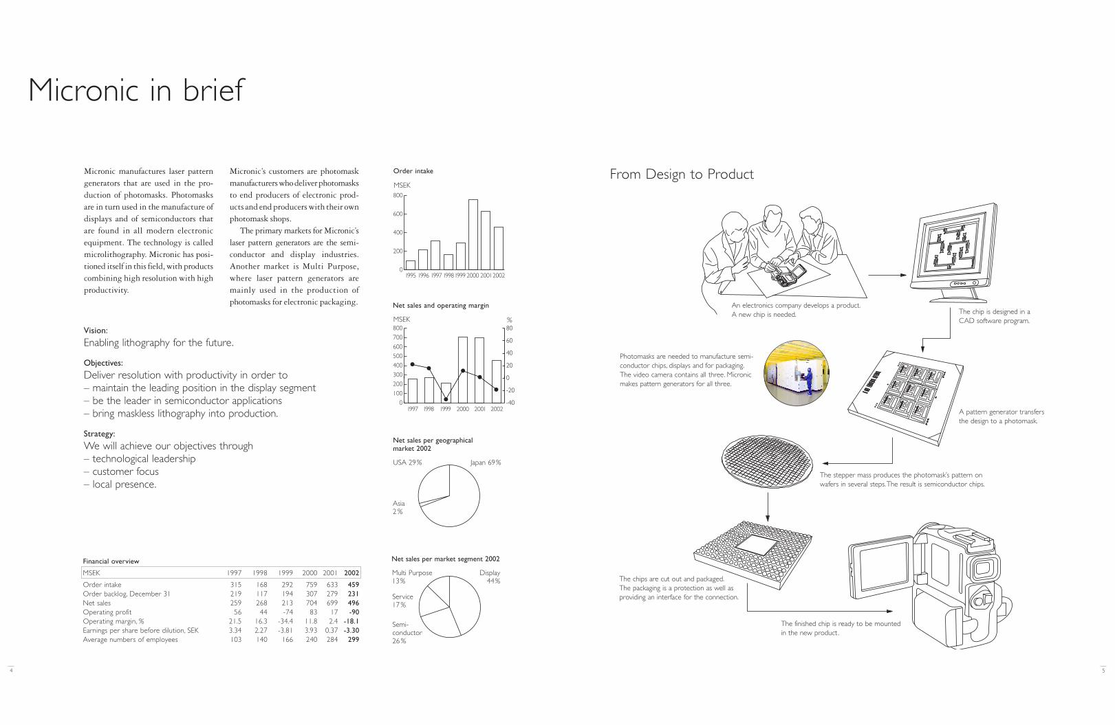
Micronic manufactures laser patterngenerators that are used in the pro-duction of photomasks. Photomasksare in turn used in the manufacture ofdisplays and of semiconductors thatare found in all modern electronicequipment. The technology is calledmicrolithography. Micronic has posi-tioned itself in this field, with productscombining high resolution with highproductivity.
Micronic’s customers are photomaskmanufacturers who deliver photomasksto end producers of electronic prod-ucts and end producers with their ownphotomask shops.
The primary markets for Micronic’slaser pattern generators are the semi-conductor and display industries.Another market is Multi Purpose,where laser pattern generators aremainly used in the production of photomasks for electronic packaging.
Micronic in brief
Vision:
Enabling lithography for the future.
Objectives:
Deliver resolution with productivity in order to – maintain the leading position in the display segment– be the leader in semiconductor applications– bring maskless lithography into production.
Strategy:
We will achieve our objectives through – technological leadership– customer focus– local presence.
0
100
200
300
400
500
600
700
800MSEK %
-40
-20
0
20
40
60
80
Net sales and operating margin
Net sales per market segment 2002
Multi Purpose 13%
Display 44%
Service17 %
Semi-conductor26 %
Net sales per geographical market 2002
Japan 69%USA 29%
Asia 2 %
0
200
400
600
800
MSEK
Order intake From Design to Product
The stepper mass produces the photomask’s pattern onwafers in several steps.The result is semiconductor chips.
The chip is designed in aCAD software program.
An electronics company develops a product.A new chip is needed.
A pattern generator transfersthe design to a photomask.
The chips are cut out and packaged.The packaging is a protection as well asproviding an interface for the connection.
The finished chip is ready to be mounted in the new product .
Photomasks are needed to manufacture semi-conductor chips, displays and for packaging.The video camera contains all three. Micronicmakes pattern generators for all three.
Financial overview
MSEK 1997 1998 1999 2000 2001 2002
Order intake 315 168 292 759 633 459Order backlog, December 31 219 117 194 307 279 231Net sales 259 268 213 704 699 496Operating profit 56 44 -74 83 17 -90Operating margin, % 21.5 16.3 -34.4 11.8 2.4 -18.1Earnings per share before dilution, SEK 3.34 2.27 -3.81 3.93 0.37 -3.30Average numbers of employees 103 140 166 240 284 2991) Vinst per aktie baseras på antal aktier vid årets slut.
6
This is the equipment that images thephotomask’s pattern on the wafer –and which can optically generate eventhe smallest structures produced bythe industry. It is the resolution – thecapacity to write the smallest detailson the photomask – that is decisive increating both customer interest andthe necessary prerequisites for busi-ness within the most advanced, andtherefore most commercially interest-ing, market segment. During the yearwe have had a number of meetingswith important customers where wereceived feedback that our technologymeets their resolution requirements.
The development of a new techno-logy like this, along with the accompa-nying platform, is extremely demand-ing both in terms of time and resources.It also includes a great deal of workwith the chemical process and datahandling, which must be done in closecooperation with customers and othersuppliers. Thanks to the strong effortsof our colleagues and partners, wehave made great progress this year ina number of key areas. We can now
7
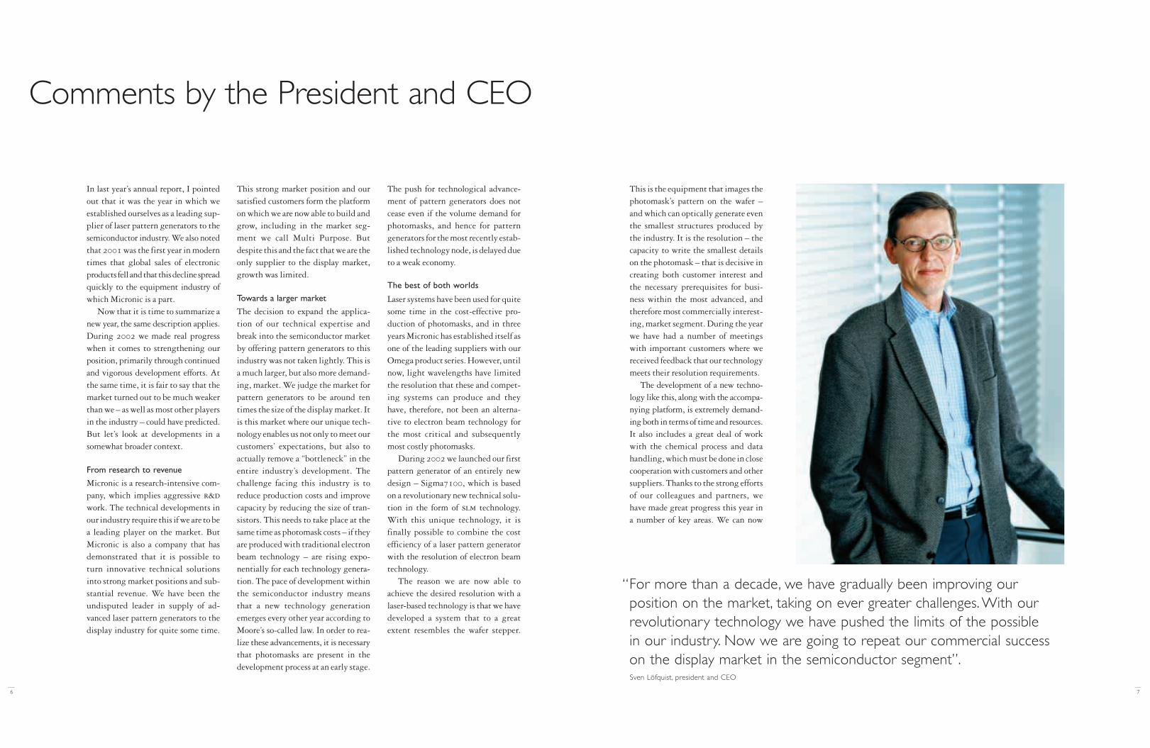
In last year’s annual report, I pointedout that it was the year in which weestablished ourselves as a leading sup-plier of laser pattern generators to thesemiconductor industry. We also notedthat 2001 was the first year in moderntimes that global sales of electronicproducts fell and that this decline spreadquickly to the equipment industry ofwhich Micronic is a part.
Now that it is time to summarize anew year, the same description applies.During 2002 we made real progresswhen it comes to strengthening ourposition, primarily through continuedand vigorous development efforts. Atthe same time, it is fair to say that themarket turned out to be much weakerthan we – as well as most other playersin the industry – could have predicted.But let’s look at developments in asomewhat broader context.
From research to revenue
Micronic is a research-intensive com-pany, which implies aggressive r&dwork. The technical developments inour industry require this if we are to bea leading player on the market. ButMicronic is also a company that hasdemonstrated that it is possible toturn innovative technical solutionsinto strong market positions and sub-stantial revenue. We have been theundisputed leader in supply of ad-vanced laser pattern generators to thedisplay industry for quite some time.
This strong market position and oursatisfied customers form the platformon which we are now able to build andgrow, including in the market seg-ment we call Multi Purpose. Butdespite this and the fact that we are theonly supplier to the display market,growth was limited.
Towards a larger market
The decision to expand the applica-tion of our technical expertise andbreak into the semiconductor marketby offering pattern generators to thisindustry was not taken lightly. This isa much larger, but also more demand-ing, market. We judge the market forpattern generators to be around tentimes the size of the display market. Itis this market where our unique tech-nology enables us not only to meet ourcustomers’ expectations, but also toactually remove a “bottleneck” in theentire industry’s development. Thechallenge facing this industry is toreduce production costs and improvecapacity by reducing the size of tran-sistors. This needs to take place at thesame time as photomask costs – if theyare produced with traditional electronbeam technology – are rising expo-nentially for each technology genera-tion. The pace of development withinthe semiconductor industry meansthat a new technology generationemerges every other year according toMoore’s so-called law. In order to rea-lize these advancements, it is necessarythat photomasks are present in thedevelopment process at an early stage.
The push for technological advance-ment of pattern generators does notcease even if the volume demand forphotomasks, and hence for patterngenerators for the most recently estab-lished technology node, is delayed dueto a weak economy.
The best of both worlds
Laser systems have been used for quitesome time in the cost-effective pro-duction of photomasks, and in threeyears Micronic has established itself asone of the leading suppliers with ourOmega product series. However, untilnow, light wavelengths have limitedthe resolution that these and compet-ing systems can produce and theyhave, therefore, not been an alterna-tive to electron beam technology forthe most critical and subsequentlymost costly photomasks.
During 2002 we launched our firstpattern generator of an entirely newdesign – Sigma7100, which is basedon a revolutionary new technical solu-tion in the form of slm technology.With this unique technology, it isfinally possible to combine the costefficiency of a laser pattern generatorwith the resolution of electron beamtechnology.
The reason we are now able toachieve the desired resolution with alaser-based technology is that we havedeveloped a system that to a greatextent resembles the wafer stepper.
Comments by the President and CEO
“For more than a decade, we have gradually been improving our position on the market, taking on ever greater challenges. With our revolutionary technology we have pushed the limits of the possible in our industry. Now we are going to repeat our commercial success on the display market in the semiconductor segment”.Sven Löfquist, president and CEO
0
50
100
150
200
250
300
350
SEK
010002000300040005000
m a m j j a s o n d j f m a m j j a s o n d j f m a m j j a s s o n d20012000 2002
Number thousands
Micronic Laser SystemsAfv General Index
Traded number of shares,weekly, thousandsNasdaq 100 Idx
state that the Sigma platform contain-ing our unique slm technology meetsour expectations and has all the pre-requisites to be a commercial success.The platform we’ve built is scalableand can therefore be used in the nextseveral generations of semiconductortechnology. Additionally, by the endof the year we were able to launch theSigma7300, the second generationSigma system, which will be used inthe manufacture of photomasks forthe 65 nanometer technology node.
On the road towards maskless lithography
Our slm technology has proven that itcan be used for more than merelyoffering the industry efficient laserpattern generators. To complementthe traditional manufacturing processwith a lithography method withoutthe costly photomask for prototypeand small series production, so-calledmaskless lithography, has always beena vision for the industry. As the costsfor photomasks increase exponential-ly, this concept becomes more inter-esting from an economic point of view.Our slm technology, which is built on the wafer stepper concept, makesmaskless lithography in semiconductormanufacturing commercially feasiblefor the first time.
Maskless lithography is also aneffective way for Micronic to capital-ize on the considerable investmentswe have made to develop slm techno-logy through diversifying its applica-tions. In close cooperation with asml,we have already made an initial system
design and completed studies whichindicate very good market possibilities.
The year in brief
To summarize, 2002 was a very weakyear from a market perspective - muchworse than 2001. To this we can addthe weakening of the dollar againstthe Swedish krona, our accountingcurrency. In spite of low sales figures,Micronic held its ground and defen-ded its market position in three pro-duct areas – namely semiconductor,display and Multi Purpose.
As for our future positions, we havecontinued to invest in critical researchand development. In parallel with thecontinuing development work, wehave also substantially strengthenedour patent protection surroundingour key technology in order to secureour investment.
Internally, we have worked hard oncutting costs and adapting to weakermarket conditions. We have reducedour workforce by approximately 10 percent, something which wasabsolutely necessary. We have alsostreamlined our organization and canreport a radical reduction in expendi-ture during the second half of the yearcompared to the first. During the yearwe finished the considerable invest-ments we have been making in ourprocess laboratory and installed a newbusiness system.
Outlook for 2003After yet another weak year where themarket has been characterized by tech-nology investments, we know thatthere is a significant investmentrequirement in the market as soon asthe demand for semiconductor com-ponents takes off. When this need willtranslate into an increase in orders anddeliveries is difficult to predict as it iscontrolled by the manufacturers eva-luation of the end market. We willcontinue to work towards the goal oftransforming our intensive develop-ment efforts into commercial successeseven in a continued weak market cha-racterized by technology investments.We will continue to stand strong withour broad range of products when thesemiconductor market experiencesrevival. We will also continue work onpromotion of maskless lithographywith the goal of getting potential cus-tomers on board for the funding offuture activities.
We have demonstrated that it ispossible in the display market toachieve a strong and profitable posi-tion through technical leadership andefficient customer support. Our goalis to achieve the same in the semicon-ductor market. We have the technicalsolutions, a good organization, com-petent and loyal staff – and our cus-tomers want us to succeed!
Sven LöfquistPresident and CEO
8
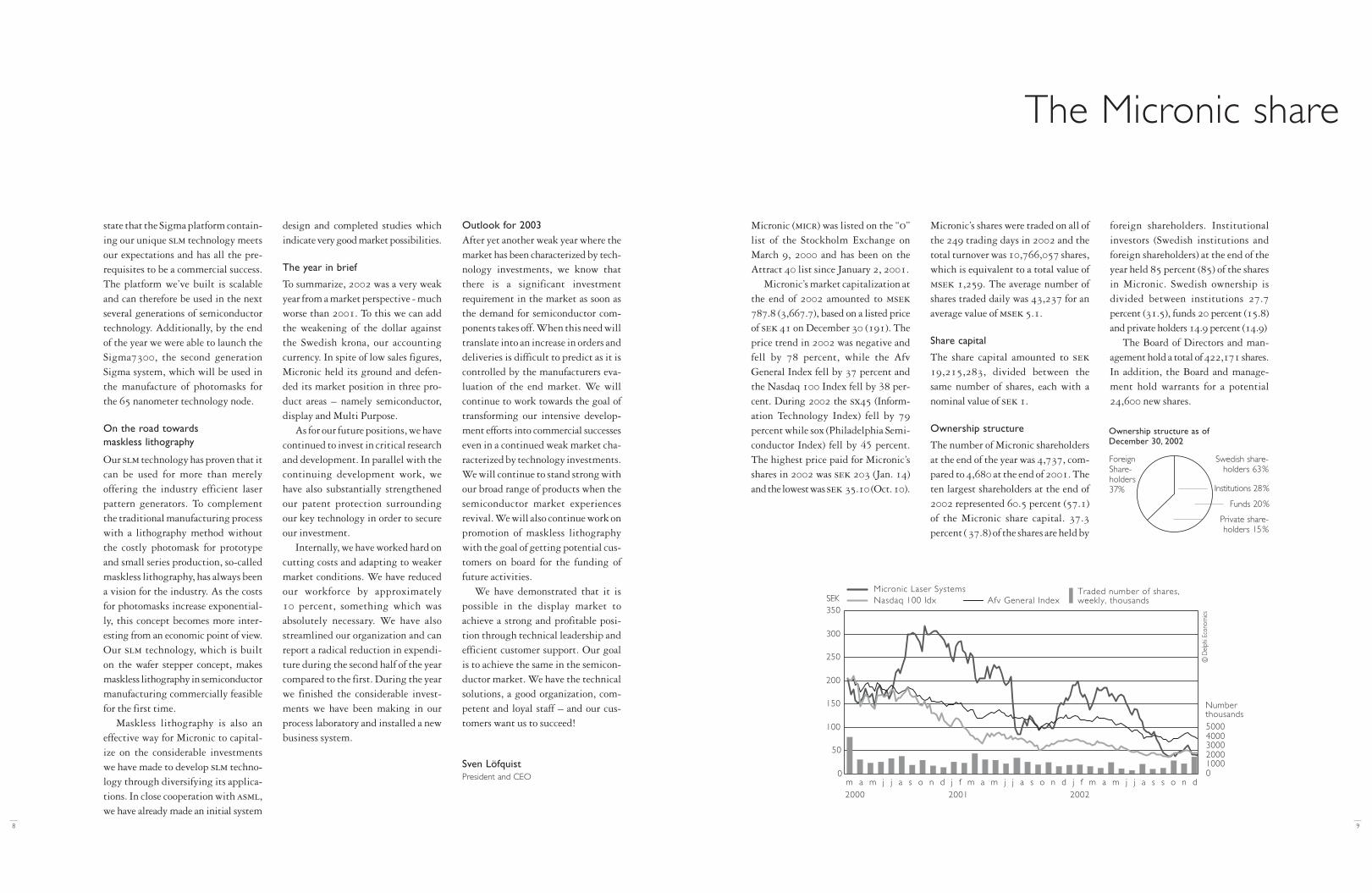
Micronic (micr) was listed on the “o”list of the Stockholm Exchange onMarch 9, 2000 and has been on theAttract 40 list since January 2, 2001.
Micronic’s market capitalization atthe end of 2002 amounted to msek787.8 (3,667.7), based on a listed priceof sek 41 on December 30 (191). Theprice trend in 2002 was negative andfell by 78 percent, while the AfvGeneral Index fell by 37 percent andthe Nasdaq 100 Index fell by 38 per-cent. During 2002 the sx45 (Inform-ation Technology Index) fell by 79percent while sox (Philadelphia Semi-conductor Index) fell by 45 percent.The highest price paid for Micronic’sshares in 2002 was sek 203 (Jan. 14)and the lowest was sek 35.10 (Oct. 10).
Micronic’s shares were traded on all ofthe 249 trading days in 2002 and thetotal turnover was 10,766,057 shares,which is equivalent to a total value ofmsek 1,259. The average number ofshares traded daily was 43,237 for anaverage value of msek 5.1.
Share capital
The share capital amounted to sek19,215,283, divided between thesame number of shares, each with anominal value of sek 1.
Ownership structure
The number of Micronic shareholdersat the end of the year was 4,737, com-pared to 4,680 at the end of 2001. Theten largest shareholders at the end of2002 represented 60.5 percent (57.1)of the Micronic share capital. 37.3percent ( 37.8) of the shares are held by
foreign shareholders. Institutionalinvestors (Swedish institutions andforeign shareholders) at the end of theyear held 85 percent (85) of the sharesin Micronic. Swedish ownership isdivided between institutions 27.7percent (31.5), funds 20 percent (15.8)and private holders 14.9 percent (14.9)
The Board of Directors and man-agement hold a total of 422,171 shares.In addition, the Board and manage-ment hold warrants for a potential24,600 new shares.
9
The Micronic share
Ownership structure as of December 30, 2002
Foreign Share-holders 37%
Swedish share- holders 63%
Institutions 28%
Funds 20%
Private share-holders 15%
1110
In addition to the above-mentionedwarrant programs, asml is entitledthrough a convertible debenture ofmsek 320, until July 31, 2004, tosubscribe for one million new shares,equivalent to approximately five per-
cent of the total number of shares inthe company.
After full dilution of warrants andconversion of debenture the totalnumber of shares could amount to21,551,333.
Dividend policy
Micronic has not paid out any divi-dends since the company was foun-ded. The company does not expect topay out dividends over the next fewyears but instead intends to retain anyearnings generated to finance furtherdevelopment projects as well as mar-keting and sales efforts.
Micronic’s warrant program
Since 1997 Micronic has implemen-ted warrant programs on five occa-sions. Four of these programs wereaimed at the employees. At the end ofthe year, the company had three war-rant programs running, with durationup until the end of 2005.
The fourth warrant program, whichwas launched in 1999 in connectionwith an order for Omega6000 fromDuPont Photomasks, involves 736,050warrants entitling holders to sub-scribe for the same number of shares.The warrants can be exercised duringthe period January 1, 2000 to Decem-ber 31, 2003 and the subscriptionprice is sek 60. The equity warrantswere allotted to DuPont in installmentspursuant to an agreement betweenMicronic and DuPont and all of thewarrants have fully been allotted.
In 2001, further warrant programs,aimed at all of the employees in theGroup, were launched.
These programs involve 380,000,130,000 and 90,000 warrants respec-tively, entitling holders to subscribefor the same number of shares. Swedishemployees are entitled to subscribe forthe shares during the period October 1,2003 until December 31, 2003 at aprice of sek 312 per share (a total of510,000 shares). Employees of foreignsubsidiaries are entitled to subscribefor 90,000 shares for a price of sek 208per share during the period October 1,2005 until December 31, 2005. Thetotal number of unallotted warrants asof December 31, 2002 was 238,500.
At the end of 2002 a warrant pro-gram launched in 1999 aimed at theemployees expired. The subscriptionprice was sek 90 and the outstandingwarrants expired without being con-verted into shares.
Warrant program
Program 4 5/6 7
Subscription period from Jan. 1, 2000 Oct. 1, 2003 Oct. 1, 2005Subscription period until Dec. 31, 2003 Dec. 31, 2003 Dec. 31, 2005Subscription price 60 312 208Board and President 8,800Management 12,800 3,000Other employees1) 301,900 35,000External business partners 736,050Unallotted 2) 186,500 52,000Total 736,050 510,000 90,000
1) The Chairman of the Board holds 4,400 warrants.2) The remaining unallotted warrants have not been given a value in the accounts.
Changes in share capital
Increase in Total no. Total shareYear Transaction no. of shares of shares capital, SEK
1989 Company founded 500 50,0001989 New issue 9,500 10,000 1,000,0001989 New issue 6,000 16,000 1,600,0001990 New issue 3,300 19,300 1,930,0001994 New issue 1,801 21,101 2,110,1001997 Share dividend 5:1 84,404 105,505 10,550,5001997 Split 100:1 10,444,995 10,550,500 10,550,5001997 New issue 1,450,000 12,000,500 12,000,5001998 New issue 2,000,083 14,000,583 14,000,5832000 New issue 4,500,000 18,500,583 18,500,5832000 Exercise of equity warrants 600,000 19,100,583 19,100,5832001 Exercise of equity warrants 102,000 19,202,583 19,202,5832002 Exercise of equity warrants 12,700 19,215,283 19,215,283
Number of shares, taking into consideration equity warrants and convertible debenture
Number of outstanding shares as of December 31, 2002 19,215,283Outstanding equity warrants 1,336,050No. of shares after equity warrants are exercised 20,551,333Convertible debenture issued to ASML 1,000,000Number of shares after full conversion 21,551,333
The following analysts monitor Micronic on a continuous basis
Analyst Telephone e-mail
Alfred Berg Patrick Clase +46 (0)8 572 360 30 [email protected] Martin Nilsson +46 (0)8 676 88 00 [email protected] Agricole Indosuez Cheuvreux Johan Eliason +46 (0)8 723 51 77 [email protected] Bank AG David Halldén +46 (0)8 463 55 15 [email protected] Securities Johan Grabe +46 (0)8 522 295 00 [email protected] Anders Berg +46 (0)8 407 80 25 [email protected] Frans Heijbel +46 (0)8 407 80 29 [email protected] Markets Jonas Eixmann +46 (0)8 701 16 81 [email protected] Securities Mattias Eriksson +46 (0)8 506 520 62 [email protected] Nordiska Mikael Laséen +46 (0)8 791 48 27 [email protected] Urban Ekelund +46 (0)8 545 013 31 [email protected] Roger Jansson +46 (0)8 545 013 30 [email protected] Securities Robert Ahldin +46 (0)8 454 32 00 [email protected] Mats Larsson +46 (0)8 585 925 42 [email protected] Research Brett Simpson +44 (0)20 795 913 20 [email protected]
Data per share is presented in Financial key ratios on page 32.
Shareholding in Micronic by size
No. of No. of sharesSize of holding shareholders and votes %
More than 100,000 26 13,316,740 69.3050,001-100,000 29 2,005,216 10.4410,001-50,000 78 1,935,176 10.075,001-10,000 46 355,630 1.852,001-5,000 117 395,065 2.061,001-2,000 170 268,044 1.39501-1,000 407 352,066 1.831-500 3,864 587,346 3.06
Total 4,737 19,215,283 100,00
Micronic´s ten largest shareholders as per December 30, 2002
Shareholder Number of shares %
Stiftelsen Industrifonden 3,500,000 18.2Capital Group Funds 2,096,976 10.9Salomon Smith Barney 950,000 4.9JP Morgan Chase Bank 925,937 4.8Robur Funds 815,234 4.2Skandia 712,750 3.7Banco Funds 703,490 3.7Skandia Carlson Funds 686,049 3.6Nordea Funds 682,000 3.6Fidelity Funds 552,282 2.9Total the 10 largest shareholders 11,624,718 60.5Other holders 7,590,565 39.5Total outstanding shares 19,215,283 100.0
Micronic’s customers possess consider-able expertise in the field of pho-tomask production and understand-ing of what is required of pattern gene-rators. Micronic works with its custo-mers on development projects to meetthe market’s new demands.
The customers force the pace ofproduct development and also help toincrease Micronic’s expertise. In certain
cases customers also expand the appli-cation areas and markets for Micronic’spattern generators.
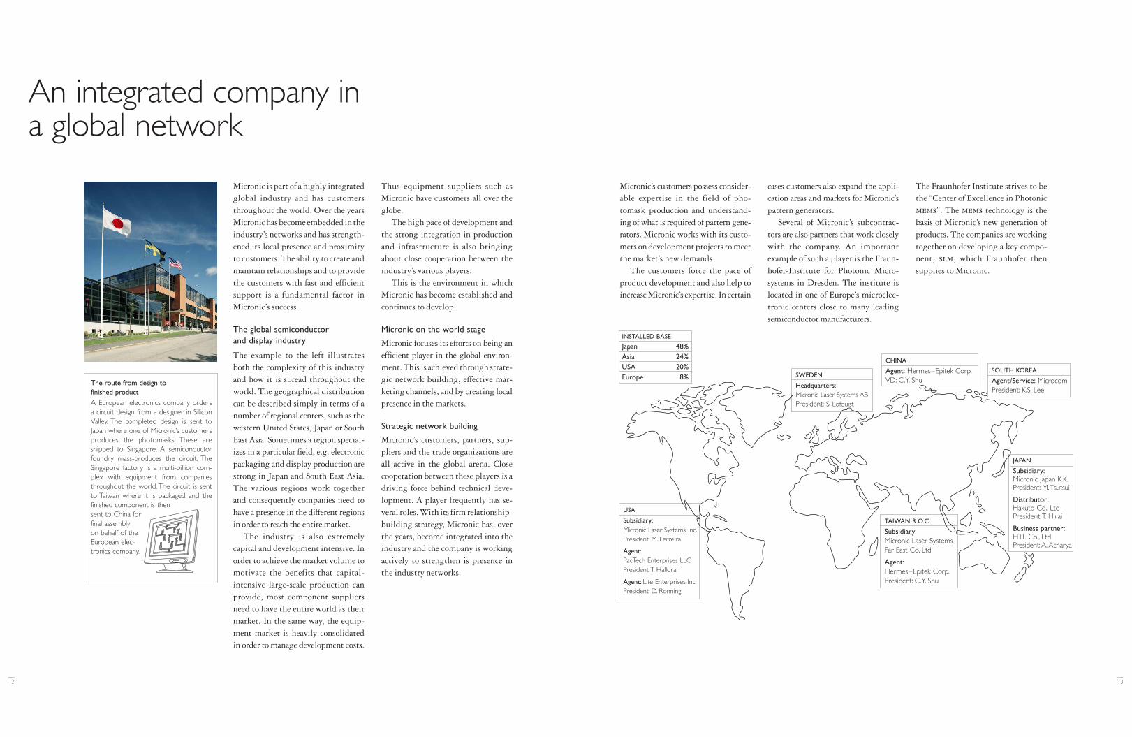
Several of Micronic’s subcontrac-tors are also partners that work closelywith the company. An importantexample of such a player is the Fraun-hofer-Institute for Photonic Micro-systems in Dresden. The institute islocated in one of Europe’s microelec-tronic centers close to many leadingsemiconductor manufacturers.
The Fraunhofer Institute strives to bethe “Center of Excellence in Photonicmems”. The mems technology is thebasis of Micronic’s new generation ofproducts. The companies are workingtogether on developing a key compo-nent, slm, which Fraunhofer thensupplies to Micronic.
13
Micronic is part of a highly integratedglobal industry and has customersthroughout the world. Over the yearsMicronic has become embedded in theindustry’s networks and has strength-ened its local presence and proximityto customers. The ability to create andmaintain relationships and to providethe customers with fast and efficientsupport is a fundamental factor inMicronic’s success.
The global semiconductor and display industry
The example to the left illustratesboth the complexity of this industryand how it is spread throughout theworld. The geographical distributioncan be described simply in terms of anumber of regional centers, such as thewestern United States, Japan or SouthEast Asia. Sometimes a region special-izes in a particular field, e.g. electronicpackaging and display production arestrong in Japan and South East Asia.The various regions work togetherand consequently companies need tohave a presence in the different regionsin order to reach the entire market.
The industry is also extremelycapital and development intensive. Inorder to achieve the market volume tomotivate the benefits that capital-intensive large-scale production canprovide, most component suppliersneed to have the entire world as theirmarket. In the same way, the equip-ment market is heavily consolidatedin order to manage development costs.
Thus equipment suppliers such asMicronic have customers all over theglobe.
The high pace of development andthe strong integration in productionand infrastructure is also bringingabout close cooperation between theindustry’s various players.
This is the environment in whichMicronic has become established andcontinues to develop.
Micronic on the world stage
Micronic focuses its efforts on being anefficient player in the global environ-ment. This is achieved through strate-gic network building, effective mar-keting channels, and by creating localpresence in the markets.
Strategic network building
Micronic’s customers, partners, sup-pliers and the trade organizations areall active in the global arena. Closecooperation between these players is adriving force behind technical deve-lopment. A player frequently has se-veral roles. With its firm relationship-building strategy, Micronic has, overthe years, become integrated into theindustry and the company is workingactively to strengthen is presence inthe industry networks.
An integrated company in a global network
12
The route from design to finished product
A European electronics company ordersa circuit design from a designer in SiliconValley. The completed design is sent toJapan where one of Micronic’s customersproduces the photomasks. These areshipped to Singapore. A semiconductorfoundry mass-produces the circuit. TheSingapore factory is a multi-billion com-plex with equipment from companiesthroughout the world. The circuit is sentto Taiwan where it is packaged and thefinished component is then sent to China forfinal assembly on behalf of theEuropean elec-tronics company.
SWEDEN
Headquarters:Micronic Laser Systems ABPresident: S. Löfquist
USA
Subsidiary:Micronic Laser Systems, Inc.President: M. Ferreira
Agent:PacTech Enterprises LLCPresident:T. Halloran
Agent: Lite Enterprises IncPresident: D. Ronning
CHINA
Agent: Hermes–Epitek Corp.VD: C.Y. Shu
JAPAN
Subsidiary:Micronic Japan K.K.President: M.Tsutsui
Distributor:Hakuto Co., LtdPresident:T. Hirai
Business partner:HTL Co., LtdPresident:A.Acharya
TAIWAN R.O.C.
Subsidiary:Micronic Laser SystemsFar East Co, Ltd
Agent:Hermes–Epitek Corp.President: C.Y. Shu
INSTALLED BASE
Japan 48%Asia 24%USA 20%Europe 8%
SOUTH KOREA
Agent/Service: MicrocomPresident: K.S. Lee
In Micronic’s largest markets – Japanand the usa – Micronic has built up aservice organization. In addition toMicronic’s own service organization,the company has established servicepartnerships with the local agents,Microcom in South Korea and Hermes-Epitek in Taiwan. The customer sup-port organization in Sweden providessupport for the local service organiza-tions and its primary function is tosupply expert technical support andspare parts, and to ensure that skillsdevelopment takes place within thelocal companies.
China is a growing market, not least forMicronic, and in 2002 the companyopened a local office in Shanghai. InTaiwan the service organization wasconverted into a subsidiary.
15
Micronic is also involved in coopera-tion in broader contexts, such as stan-dardization work with trade organiza-tions. One such trade organization,semi (Semiconductor Equipment andMaterials International), is running anumber of projects within the semi-conductor and display industry andMicronic is participating in theseprojects. semi is, for example, headinga consortium of software companies,semiconductor manufacturers, pho-tomask producers and equipmentmanufacturers who are working onproducing a new data format namedoasis. Micronic is making a significantcontribution to this project. oasis willbe better able to handle the enormousvolume of data that is currently a causeof the high costs and long productiontimes linked to producing advancedphotomasks.
Global marketing channels
The number of customers is limited,therefore is direct contact with cus-tomers an important part of the salesprocess. Micronic conducts its mar-keting activities in cooperation withagents and distributors. They worktogether with Micronic troughout thewhole selling process and in JapanMicronic participates in trade showsthrough its local distributor Hakutoand in Taiwan through the local agentHermes-Epitek.
Micronic has a strong network ofindustry and technical experts who arein close contact with Micronic as wellas the company’s customers. These“ambassadors” participate in technicaldiscussions and sales activities.
Another marketing channel con-sists of the trade fairs arranged amongothers by semi around the world.Micronic has the opportunity to pre-sent scientific reports at the scientificconferences that are important to pho-tomask manufacturers and that areorganized by spie (InternationalSociety for Optical Engineering) andsid (Society for Information Display).In 2002 Micronic presented reports atfive such conferences.
Finally, successful product launchesare of great significance for how a pro-duct is received in the market. Apartfrom being good reference installa-tions, a successful launch also oftenresult in an increased demand for pho-tomasks produced by the product.
Global organization with a strong local presence
Factors such as shrinking productcycles and the ambition among semi-conductor and display manufacturersto reduce the time from product con-cept to the launch of new productsrequire a fast and efficient delivery ofphotomasks. A delayed photomaskdelivery is often extremely costly for theend customer. Photomask manufactu-rers are therefore dependent on both fastproduction and reliable equipment.
Efficient service and customer sup-port for production equipment isessential, and this is especially true forMicronic.
By having a strong local serviceorganization close to the customer,Micronic can ensure that its custo-mers’ service and installation require-ments are met. Many of Micronic’sinstalled laser pattern generators arein Japan where the majority of themost advanced photomasks for dis-plays are produced. Micronic also hasa large installed base of systems forphotomasks for display manufacturein South Korea and numerous elec-tronic packaging systems installed inAsia and the usa. The need for a glob-al service organization close to the cus-tomer has further increased in connec-tion with Micronic’s breakthroughinto the market for laser pattern gen-erators for the semiconductor market.These installations generally requiremore support at the same time as thecustomer base is more geographicallydispersed than in Micronic’s othermarkets which are concentrated inAsia.
14
“Pushing the limits is about always daring to venture into unchartedterritory. I try to take on new challenges all the time.This enables me to shatter the limits.To succeed, you need to communicate frequently and work closely with your colleagues as well as your customers, and you need an open mind”.Tomokazu Matsushita, service engineer, Japan
Computers and wireless communi-cation are the driving forces of the semiconductor industry. They are the dominant segments in the electronicsindustry and are behind economicgrowth in the semiconductor sector.During 2002, the state of economiesaround the world and low computersales, as well as weak development inthe mobile communication market,have resulted in a continued weaksemiconductor market.
At the same time, the demand forincreasing numbers of increasinglysmall transistors in circuits is pushingforward semiconductor development.The shrinking size of electronics com-ponents is leading to the developmentof new applications, such as morepowerful electronic products andlower energy consumption in portableproducts. Increased transistor packingdensity in circuits is also needed in orderto manage production costs. The desirefor new products, together with theindustry’s financial conditions, is lead-ing to smaller and smaller transistors.
In 2002 the suppliers of equip-ment used in semiconductor produc-tion experienced a weak demand fortheir products while at the same timeperformance requirements continuedto increase.
Photomask manufacturers cameunder a similar kind of pressure, expe-riencing lower sales volumes while atthe same time finding it necessary toinvest in equipment for the next tech-nology node.
Micronic in the semiconductor segment
Micronic’s product strategy is to deliverthe required precision with a strongfocus on the industry’s costs structure.Micronic markets two product seriesin the semiconductor segment –Omega6000 and Sigma7000.
In 1999 Micronic made its break-through in the market for laser patterngenerators for the semiconductor in-dustry with the launch of the Omega-6000 series. The series is used for tech-nology nodes down to 130nanometers.
As transistors become smaller, therequirements of microlithography andphotomasks become greater, whichleads to increasingly expensive photo-masks. The general consensus withinthis branch is that the estimated costof a mask set for a semiconductor cir-cuit for the 90 nanometer technologynode is musd 1,5–2. This is doublethe amount that a mask set can cost for130 nanometer and eight times morethan the usd 250,000 for a mask setfor 180 nanometer. The escalatingcosts are threatening the semiconduc-tor industry because fewer new circuitdesigns are being tested.
The anticipated high costs for the 90nanometer technology node are partlyrelated to the long photomask writetimes. The industry is expecting toproduce the critical photomasks withelectron-beam technology, which pro-vides high resolution but is slow. Inthe case of earlier technology nodes,most of the photomasks were producedusing the faster laser technology.
With our unique slm technology,which combines high resolution withhigh throughput in the Sigma7000product series, Micronic can offer theindustry a means of curbing the run-away costs. Sigma7000 enables manu-facturers of photomasks to use thefaster laser technology for criticalphotomasks for the 90nanometer tech-nology node. The first Sigma systemwas shipped during the second quarterand in December Sigma7300 waslaunched.
Several of Micronic’s competitorsoffer pattern generators based on elec-tron beam technology. These areToshiba Machine Co. Ltd, Jeol Co.Ltd., Hitachi Co. Ltd. and Etec, anApplied Materials company. In addi-tion to Micronic, Etec also manufac-tures laser pattern generators.
The semiconductor market:laser technology paves the way
16
The semiconductor segment in figures
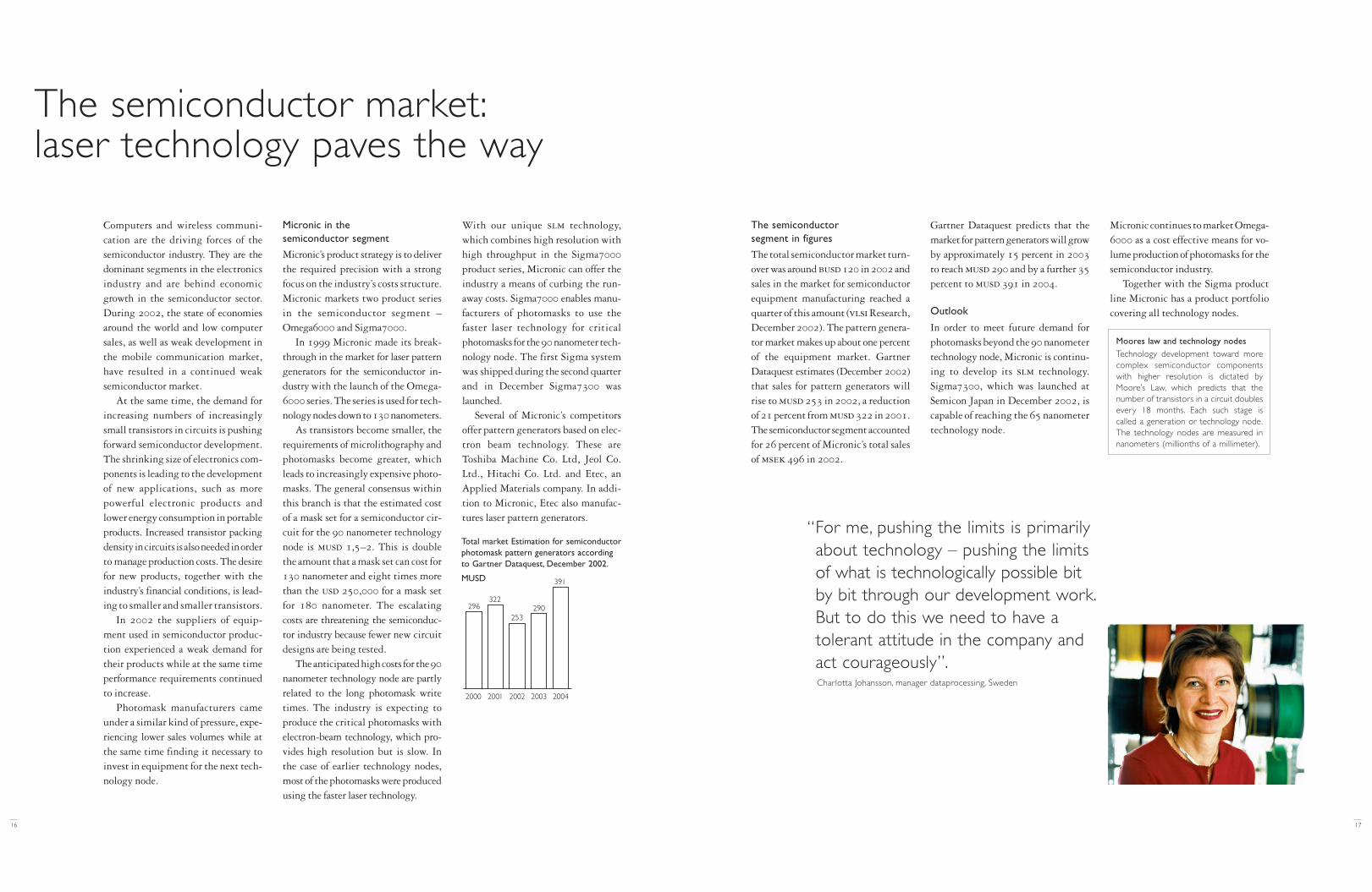
The total semiconductor market turn-over was around busd 120 in 2002 andsales in the market for semiconductorequipment manufacturing reached aquarter of this amount (vlsi Research,December 2002). The pattern genera-tor market makes up about one percentof the equipment market. GartnerDataquest estimates (December 2002)that sales for pattern generators willrise to musd 253 in 2002, a reductionof 21 percent from musd 322 in 2001.The semiconductor segment accountedfor 26 percent of Micronic’s total salesof msek 496 in 2002.
Gartner Dataquest predicts that themarket for pattern generators will growby approximately 15 percent in 2003to reach musd 290 and by a further 35percent to musd 391 in 2004.
Outlook
In order to meet future demand forphotomasks beyond the 90 nanometertechnology node, Micronic is continu-ing to develop its slm technology.Sigma7300, which was launched atSemicon Japan in December 2002, iscapable of reaching the 65 nanometertechnology node.
Micronic continues to marketOmega-6000 as a cost effective means for vo-lume production of photomasks for thesemiconductor industry.
Together with the Sigma productline Micronic has a product portfoliocovering all technology nodes.
17
Total market Estimation for semiconductorphotomask pattern generators accordingto Gartner Dataquest, December 2002.
MUSD
“For me, pushing the limits is primarily about technology – pushing the limits of what is technologically possible bitby bit through our development work.But to do this we need to have a tolerant attitude in the company and act courageously”.Charlotta Johansson, manager dataprocessing, Sweden
Moores law and technology nodes
Technology development toward morecomplex semiconductor componentswith higher resolution is dictated byMoore’s Law, which predicts that thenumber of transistors in a circuit doublesevery 18 months. Each such stage iscalled a generation or technology node.The technology nodes are measured innanometers (millionths of a millimeter).
Micronic’s system has an extremelyhigh level of performance and a robustdesign and therefore provides goodproduction reliability. The high levelof productivity and reliability meansthat Micronic’s system has a favorablecost of ownership. Working closelywith several customers has also madeit possible to meet market require-ments at the appropriate time.
During 2002 Micronic introducedthe next generation of pdp systems, themp185+. This can write photomasks upto 1,400 x 1,850 mm, which is neces-sary for the new production lines for pdpdisplays that are under construction.
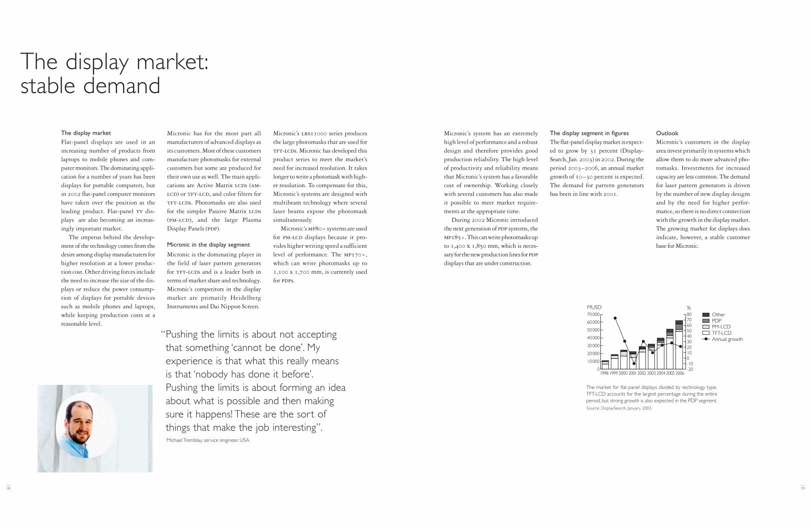
The display segment in figuresThe flat-panel display market is expect-ed to grow by 31 percent (Display-Search, Jan. 2003) in 2002. During theperiod 2003–2006, an annual marketgrowth of 10–30 percent is expected.The demand for pattern generatorshas been in line with 2001.
OutlookMicronic’s customers in the displayarea invest primarily in systems whichallow them to do more advanced pho-tomasks. Investments for increasedcapacity are less common. The demandfor laser pattern generators is drivenby the number of new display designsand by the need for higher perfor-mance, so there is no direct connectionwith the growth in the display market.The growing market for displays doesindicate, however, a stable customerbase for Micronic.
19
The display marketFlat-panel displays are used in anincreasing number of products fromlaptops to mobile phones and com-puter monitors. The dominating appli-cation for a number of years has beendisplays for portable computers, butin 2002 flat-panel computer monitorshave taken over the position as theleading product. Flat-panel tv dis-plays are also becoming an increas-ingly important market.
The impetus behind the develop-ment of the technology comes from thedesire among display manufacturers forhigher resolution at a lower produc-tion cost. Other driving forces includethe need to increase the size of the dis-plays or reduce the power consump-tion of displays for portable devicessuch as mobile phones and laptops,while keeping production costs at areasonable level.
Micronic has for the most part allmanufacturers of advanced displays asits customers. Most of these customersmanufacture photomasks for externalcustomers but some are produced fortheir own use as well. The main appli-cations are Active Matrix lcds (am-lcd) or tft-lcd, and color filters fortft-lcds. Photomasks are also usedfor the simpler Passive Matrix lcds(pm-lcd), and the large PlasmaDisplay Panels (pdp).
Micronic in the display segment
Micronic is the dominating player inthe field of laser pattern generators for tft-lcds and is a leader both interms of market share and technology.Micronic’s competitors in the displaymarket are primarily HeidelbergInstruments and Dai Nippon Screen.
Micronic’s lrs11000 series producesthe large photomasks that are used fortft-lcds. Micronic has developed thisproduct series to meet the market’sneed for increased resolution. It takeslonger to write a photomask with high-er resolution. To compensate for this,Micronic’s systems are designed withmultibeam technology where severallaser beams expose the photomasksimultaneously.
Micronic’s mp80+ systems are usedfor pm-lcd displays because it pro-vides higher writing speed a sufficientlevel of performance. The mp170+,which can write photomasks up to1,100 x 1,700 mm, is currently usedfor pdps.
The display market:stable demand
18
-20-1001020304050607080
MUSD %OtherPDPPM-LCDTFT-LCDAnnual growth
1998 1999 2000 20012002 2003 20042005 2006
The market for flat-panel displays divided by technology type.TFT-LCD accounts for the largest percentage during the entireperiod, but strong growth is also expected in the PDP segment.
“Pushing the limits is about not accepting that something ‘cannot be done’. My experience is that what this really means is that ‘nobody has done it before’.Pushing the limits is about forming an ideaabout what is possible and then making sure it happens! These are the sort of things that make the job interesting”.Michael Tremblay, service engineer, USA
Source: DisplaySearch, January 2003.
The competitors in this segment arethe same as those in the passive displaysegment because similar systems areused. Micronic has largely maintainedits position as a market and technolo-gy leader in a market that in 2002 wasunstable.
Outlook
Micronic will continue to introduceimprovements which will ensure thatthe mp systems can meet new marketrequirements. The technology requiredfor e.g. higher resolution can for themost part be derived from the moreadvanced display systems. This meansthat Micronic is well-equipped todeliver the solutions which this seg-ment requires.
21
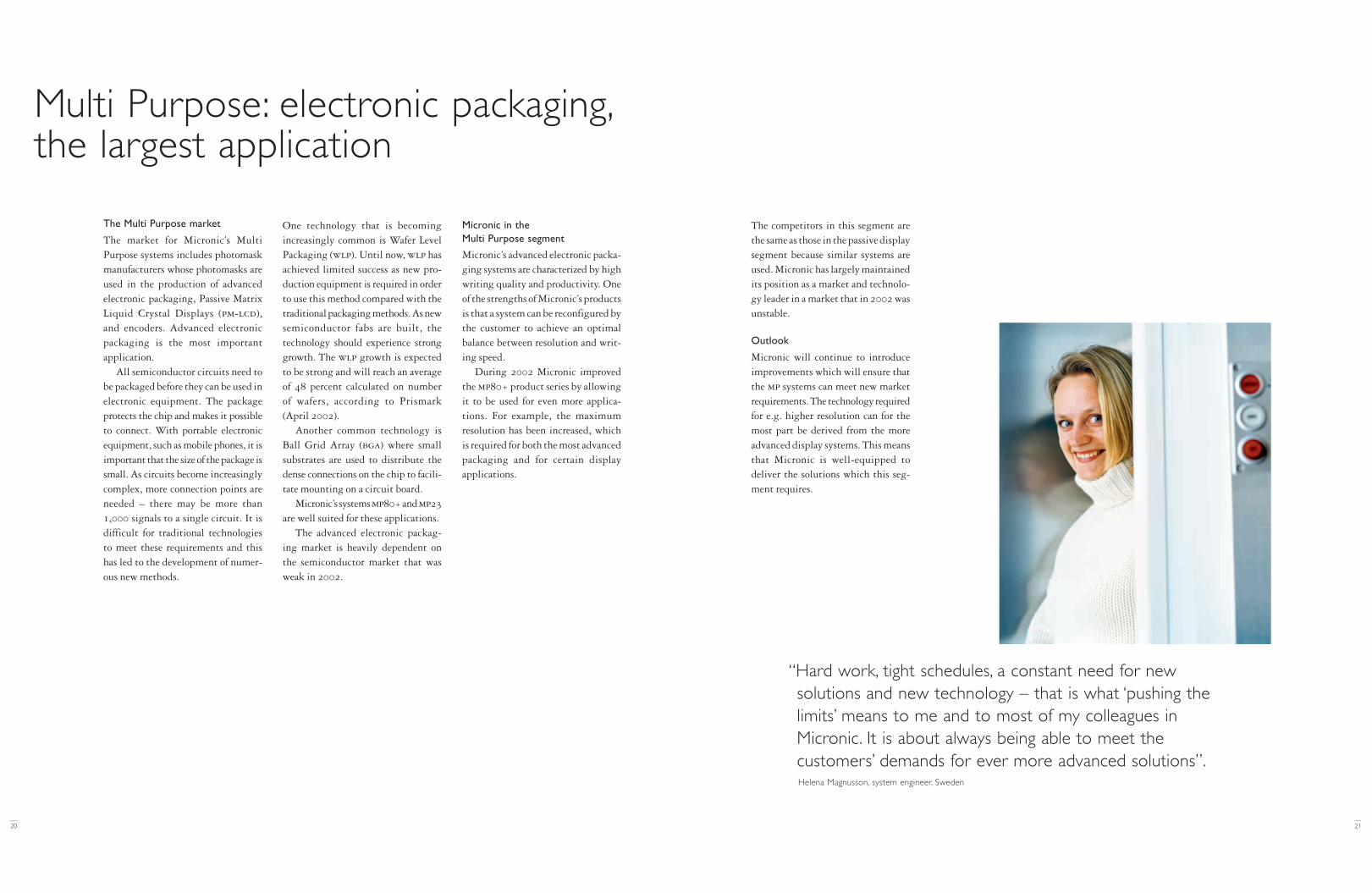
The Multi Purpose market
The market for Micronic’s MultiPurpose systems includes photomaskmanufacturers whose photomasks areused in the production of advancedelectronic packaging, Passive MatrixLiquid Crystal Displays (pm-lcd),and encoders. Advanced electronicpackaging is the most importantapplication.
All semiconductor circuits need tobe packaged before they can be used inelectronic equipment. The packageprotects the chip and makes it possibleto connect. With portable electronicequipment, such as mobile phones, it isimportant that the size of the package issmall. As circuits become increasinglycomplex, more connection points areneeded – there may be more than1,000 signals to a single circuit. It isdifficult for traditional technologiesto meet these requirements and thishas led to the development of numer-ous new methods.
One technology that is becomingincreasingly common is Wafer LevelPackaging (wlp). Until now, wlp hasachieved limited success as new pro-duction equipment is required in orderto use this method compared with thetraditional packaging methods. As newsemiconductor fabs are built, thetechnology should experience stronggrowth. The wlp growth is expectedto be strong and will reach an averageof 48 percent calculated on number of wafers, according to Prismark(April 2002).
Another common technology isBall Grid Array (bga) where smallsubstrates are used to distribute thedense connections on the chip to facili-tate mounting on a circuit board.
Micronic’s systems mp80+ and mp23are well suited for these applications.
The advanced electronic packag-ing market is heavily dependent onthe semiconductor market that wasweak in 2002.
Micronic in the Multi Purpose segment
Micronic’s advanced electronic packa-ging systems are characterized by highwriting quality and productivity. Oneof the strengths of Micronic’s productsis that a system can be reconfigured bythe customer to achieve an optimalbalance between resolution and writ-ing speed.
During 2002 Micronic improvedthe mp80+ product series by allowingit to be used for even more applica-tions. For example, the maximumresolution has been increased, whichis required for both the most advancedpackaging and for certain displayapplications.
Multi Purpose: electronic packaging,the largest application
20
“Hard work, tight schedules, a constant need for new solutions and new technology – that is what ‘pushing the limits’ means to me and to most of my colleagues in Micronic. It is about always being able to meet the customers’ demands for ever more advanced solutions”.Helena Magnusson, system engineer, Sweden
23
A constant stream of new technological challenges
22
Microlithography is an essential processin the manufacture of componentswith microscopic structures in suchproducts as displays and semiconduc-tors. Microlithography is reminiscentof how a negative is used to duplicatephotographs. Photomasks are used ina similar way to duplicate patterns ona silicon wafer or glass plate which isthen used in the production of bothsemiconductor chips and displays.
Photomask manufacturing usinglaser pattern generators
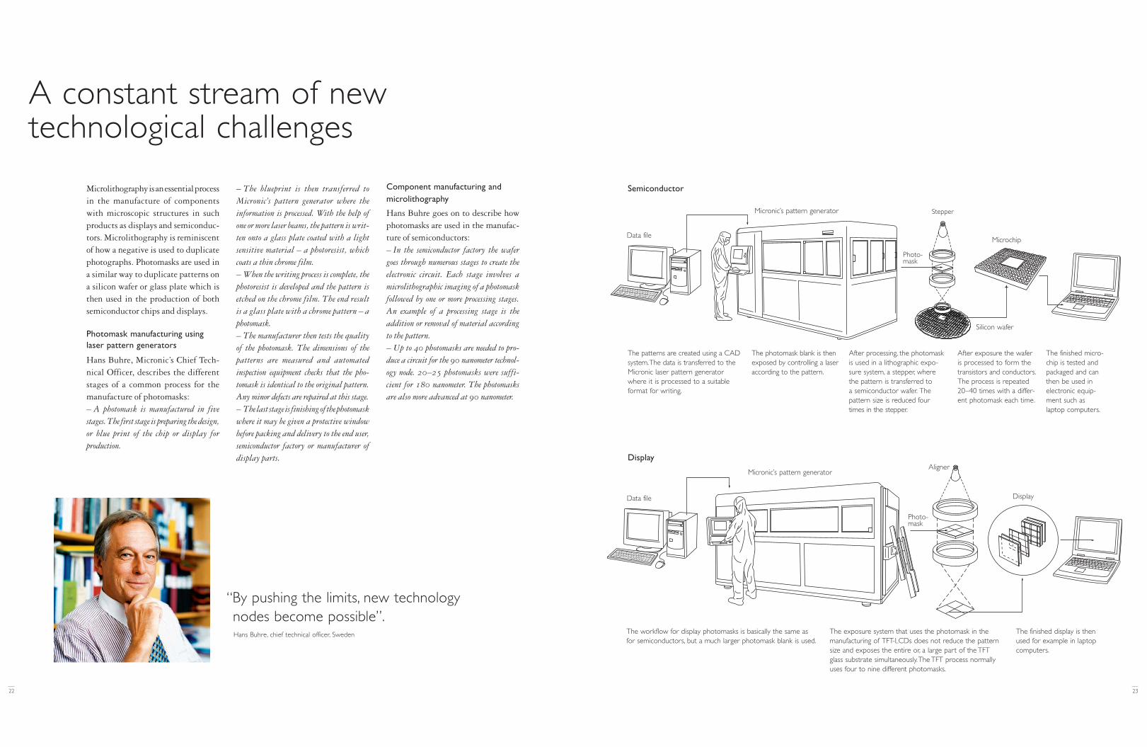
Hans Buhre, Micronic’s Chief Tech-nical Officer, describes the differentstages of a common process for themanufacture of photomasks:– A photomask is manufactured in fivestages. The first stage is preparing the design,or blue print of the chip or display for production.
– The blueprint is then transferred toMicronic’s pattern generator where theinformation is processed. With the help ofone or more laser beams, the pattern is writ-ten onto a glass plate coated with a lightsensitive material – a photoresist, whichcoats a thin chrome film.– When the writing process is complete, thephotoresist is developed and the pattern isetched on the chrome film. The end result is a glass plate with a chrome pattern – aphotomask.– The manufacturer then tests the qualityof the photomask. The dimensions of thepatterns are measured and automatedinspection equipment checks that the pho-tomask is identical to the original pattern.Any minor defects are repaired at this stage.– The last stage is finishing of the photomaskwhere it may be given a protective windowbefore packing and delivery to the end user,semiconductor factory or manufacturer ofdisplay parts.
Component manufacturing andmicrolithography
Hans Buhre goes on to describe howphotomasks are used in the manufac-ture of semiconductors:– In the semiconductor factory the wafergoes through numerous stages to create theelectronic circuit. Each stage involves amicrolithographic imaging of a photomaskfollowed by one or more processing stages.An example of a processing stage is theaddition or removal of material accordingto the pattern.– Up to 40 photomasks are needed to pro-duce a circuit for the 90 nanometer technol-ogy node. 20–25 photomasks were suffi-cient for 180 nanometer. The photomasksare also more advanced at 90 nanometer.
“By pushing the limits, new technologynodes become possible”.Hans Buhre, chief technical officer, Sweden
The finished micro-chip is tested andpackaged and canthen be used inelectronic equip-ment such as laptop computers.
Data file
Micronic’s pattern generator Stepper
Data file
Micronic’s pattern generatorAligner
The finished display is thenused for example in laptopcomputers.
Semiconductor
The patterns are created using a CADsystem.The data is transferred to theMicronic laser pattern generatorwhere it is processed to a suitableformat for writing.
The photomask blank is thenexposed by controlling a laseraccording to the pattern.
After processing, the photomask is used in a lithographic expo-sure system, a stepper, wherethe pattern is transferred to a semiconductor wafer. The pattern size is reduced fourtimes in the stepper.
After exposure the waferis processed to form thetransistors and conductors.The process is repeated20–40 times with a differ-ent photomask each time.
Display
The workflow for display photomasks is basically the same asfor semiconductors, but a much larger photomask blank is used.
The exposure system that uses the photomask in themanufacturing of TFT-LCDs does not reduce the patternsize and exposes the entire or, a large part of the TFTglass substrate simultaneously.The TFT process normallyuses four to nine different photomasks.
Microchip
Display
Photo-mask
Photo-mask
Silicon wafer
– As semiconductor circuits become increas-ingly sophisticated, the demand for packa-ging increases so that the circuits can beused in electronic equipment. This can beachieved in many different ways. One tech-nology that is becoming more common is so-called Wafer Level Packaging (WLP). Production technology exists for wlp whichuses photomasks that are big enough to exposean entire wafer in one go. An alternativetechnology, so-called step-and-repeat, usessmaller photomasks and exposes each waferin a number of stages, says Hans Buhre.
The development within the displayarea is also moving towards higherresolution. One type of tft-lcd, LowTemperature Poly Silicon (ltps) yieldssmaller transistors which means thepixel size can be reduced and the reso-lution increased. The transistors arealso getting faster which makes it pos-sible to integrate electronics directlyon the display glass.
Scanning writing principle
Micronic has built its business on theso-called raster scan technology. Thisis used in all products for the displaysegment and in electronic packaging,as well as the Omega6000 – the firstgeneration of laser pattern generatorsfor the semiconductor market. HansBuhre describes how it works:
– With Omega6000 the photomask isplaced on a so-called XY stage, a devicethat can move in two dimensions. While thestage is moving, a laser beam controlled byan acousto-optic deflector sweeps perpendi-cular to the direction of the movement of thestage. This produces a small exposed stripon the photomask.– Several strips are written in the sameway until the photomask is covered. Thetransfer of information is achieved by vary-ing the intensity of the laser beam with thehelp of an acousto-optic modulator.
2524
– A small number of photomasks are usu-ally regarded as critical including thosewhich define a transistor’s fundamentalelements, as well as the smallest details andthose most difficult to produce. Conductorpaths are then created between the transis-tors. Since millions of transistors need to beconnected and the conductor paths oftencross one another, they are laid out in sever-al layers with connections between the lay-ers, resembling an enormous ten-story roadnetwork. Most of the photomasks are usedto build the conductor structure. Lastly, thecontact structure is created so that the cir-cuit can be connected.
There are many methods for con-necting semiconductor circuits. Theyare usually built into a plastic capsulewith pins or solder balls. Micronic alsoproduces pattern generators thatwrite photomasks for this kind of elec-tronic packaging.
Display production is similar tosemiconductor production but usesfar fewer photomasks – from four tonine – but they are of a much largerformat.
Competitive technology
Hans Buhre describes two technolo-gies for writing photomasks: electronbeam and laser technology. They dif-fer in terms of precision and writingtime. – Traditionally electron beam pattern gene-rators have produced the more advancedphotomasks because they provided the high-est resolution. The laser pattern generatorshave dominated in volume production due tothe high writing speed which results in lowerphotomask costs. Micronic’s laser patterngenerators offer a unique combination of thebenefits of both of these technologies. – With the Sigma7000 series Micronic canoffer a combination of high productivity andhigh resolution and this enables us to be com-petitive in the electron beam segment as well.
Technology nodes and nanometers
Over the past twenty years, improve-ments have been made in the field ofmicrolithography as a result of signi-ficant advancements in both resolu-tion and precision. The developmenttoward more advanced pattern gener-ators with higher resolution is takingplace in stages and each stage is calleda technology node. The technologynodes are measured in nanometers(millionths of a millimeter).
– Today mass production of semiconductorsfor the 130 nanometer technology node hasbegun. Micronic’s Omega6600 patterngenerator is in operation for the productionof photomasks down to this technology nodeand preparations for the launch of a laserpattern generator that can handle future technology nodes, 90–65 nanometers, areunderway, says Hans Buhre.
Technological development is propelled by demand
The demand among consumers forincreasingly advanced electronic pro-ducts is the fundamental driving forcebehind the technological develop-ment of Micronic’s products. – In order to meet the demand for smallerand faster electronic products with higherperformance, our customers need patterngenerators that can produce photomaskswith higher resolution.
Micronic is focusing on developinglaser pattern generators to meet thedemand for increasingly sophisticatedend products.
If you enlarge a line produced with Micronic’s pattern generator to a width of 1 mm,a single strand of hair would become as large in comparison as you can see here below.
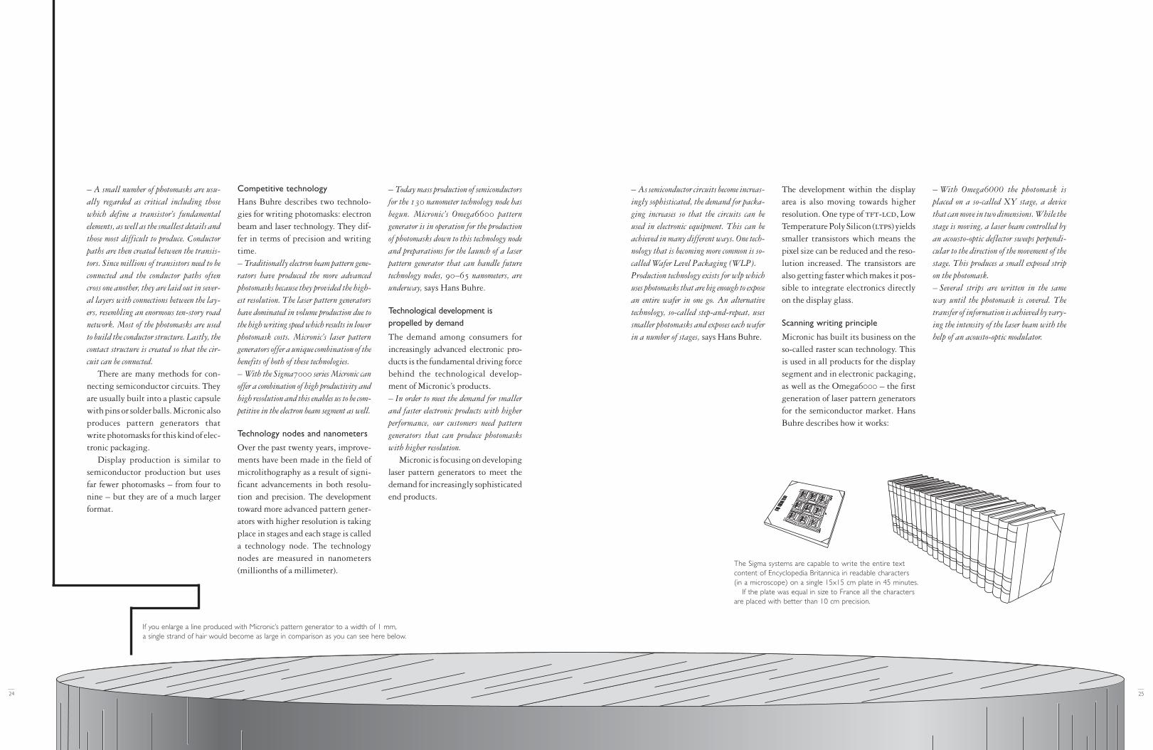
The Sigma systems are capable to write the entire text content of Encyclopedia Britannica in readable characters (in a microscope) on a single 15x15 cm plate in 45 minutes.
If the plate was equal in size to France all the charactersare placed with better than 10 cm precision.
The machines that are used to producelarge photomasks have a moving lensand a stage that only moves in onedirection. Micronic’s laser patterngenerators are available for differentphotomask sizes, up to 1,400 x 1,850millimeters.
SLM writing principle
In cooperation with the GermanFraunhofer Institute for PhotonicMicrosystems, Micronic has deve-loped a new technology called SpatialLight Modulator (slm). – SLM is the cornerstone of Micronic’sSigma system, says Hans Buhre. Sigma isbased on reflection technology whichenables pattern generation with shortwavelength lasers, resulting in very highresolution.
He explains that the heart of slmtechnology is a micromechanical cir-cuit with a million individually con-trolled mirrors that reflect the laserlight and in this way reproduce partsof the pattern. The parts are added athigh speed [frequency] until theentire pattern is joined together toform the complete construction.
– The speed of SLM technology allows usto maintain the same high productivity ofearlier generations of pattern generators,even though the resolution is higher.– Our challenge is to develop laser patterngenerator which will be able to write photo-masks for future generations of semiconduc-tors without writing times and costs sky-rocketing. The trend is moving towardhigher and higher resolution. In the case oflaser technology, it is the wavelength of thelight source used that sets the limit for how
high the resolution can be. Because SLMreflects light, this technology can be adaptedfor shorter and shorter wavelengths of thelight source to provide a higher resolutionin the future. Using products based onSLM technology, we will be able to meet ourcustomers’ needs for many years to come,concludes Hans Buhre.
Micronic’s success is based onadvanced technological knowledge.In markets that are developing at a fastpace, like those in which Micronic isactive, an aggressive approach toresearch and development is a prereq-uisite to maintain and improve thecompany’s market positions.
In 2002 Micronic invested 311msek in research and development.More than half of Micronic’s employ-ees are engaged in research and devel-opment projects.
New technology is moving Micronicinto the future
Torbjörn Sandström leads togetherwith his team at Micronics unit inGothenburg the strategic develop-ment.
– In our unit we work with technology thatis not yet available but that we intend todeliver to our customers in the future. Aboutten people work together on system analysisand system development at the point ofintersection between performance andanalysis for optics, processes and rastering.The analysis team is very important. Heredesigns are simulated on the computer beforeexperiments are conducted in the real envi-ronment. When a design that has been test-ed in the computer is considered “ready”,development continues in the design depart-ments, explains Torbjörn Sandström,and gives an example:
– We predicted at an early stage that itwas going to be difficult to generate a suf-ficiently uniform exposure with the SLM.The type of laser we were using gave a noisyimage. A doctor in the field of optics withthe relevant experience was hired. Shedesigned the exposure system based on whatwe knew about the laser. When we con-structed it, we realized that the laser’sproperties were entirely different to thosedescribed by the manufacturer and theexposure was much more uneven.We neededto analyze the laser’s properties theoretical-ly and figure out a new way of achievingan even exposure. In order to ascertain thelaser’s properties, we also constructed ameasuring device which carried out thesame measurements as the laser supplier,but more effectively, continues TorbjörnSandström.
From vision to reality
2726
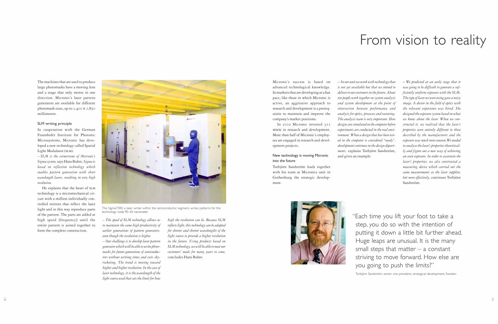
The Sigma7300, a laser writer within the semiconductor segment, writes patterns for thetechnology node 90–65 nanometer.
“Each time you lift your foot to take a step, you do so with the intention of putting it down a little bit further ahead.Huge leaps are unusual. It is the many small steps that matter – a constant striving to move forward. How else are you going to push the limits?”Torbjörn Sandström, senior vice president, strategical development, Sweden
The Sigma system, which is based onslm technology, is currently Micronic’smost advanced laser pattern generatorin the semiconductor segment. slmtechnology is also a prerequisite formaskless lithography applications.– Micronic sees possibilities with the SLMtechnology for writing directly on thewafer, so-called maskless lithography. Thelaunch of a product for maskless lithogra-phy can fundamentally change the way inwhich product development takes placewithin the semiconductor industry. Withmaskless lithography, semiconductors can bedeveloped and produced in short series.When volume production become interesting,the pattern can be transferred to photomasksfor production without any substantialchange to the product design or performance.
– A company that uses maskless lithogra-phy technology will gain several advan-tages. Certain process stages can be carriedout using maskless lithography and thissaves the cost of acquiring a photomask.Since the photomasks that are used early inthe process chain are the most difficult andhave the longest delivery time, masklesslithography can save days, weeks or evenmonths on a design. – Furthermore, the company can test seve-ral designs. Instead of excluding a round oftests because of the difficulties or the longdelivery time, maskless lithography can beused. In this way, an excessively conserva-tive design is avoided, which would other-wise result in a slower learning curve andproducts with inferior performance. – A maskless lithography system can writeseveral variations of the same constructionon one wafer and thereby provide a moreoptimized product and potentially reducethe need for reconstructions. Similarly, it ispossible to create unique circuits using mask-less lithography, for example, a machinereadable unique code can be placed on eachchip for use in quality assurance or foridentification. I believe that a functioningmaskless lithography system will lead tonew applications that we haven’t eventhought about yet, concludes TorbjörnSandström.
29
– As a result we solved the problem and wesubmitted two patent applications. Nowwe are preparing for the next stage of deve-lopment which will simplify the exposuresystem and at the same time improve thequality of the image. We managed to con-duct original and successful development inan area where it is extremely difficult tofind and buy the relevant expertise, becausethe experts in this field are few and areoften working for other companies already.
Close cooperation is a prerequisiteTo further reinforce the company’sinnovative potential, Micronic workswith external players. This includesan established collaboration withGermany’s Fraunhofer Institute.– As part of our collaboration with Fraun-hofer, we have developed the SLM technol-ogy, which is the basis of our Sigma sys-tem.Without this collaboration and theopportunity to use Fraunhofer’s equipment,it would not have been possible to developthis technology, says Torbjörn Sandström.For Fraunhofer a partnership withMicronic is an important channel forcommercialization of inventions andpatents within slm technology.
An important aspect of our research anddevelopment work is our focus onpatents. Micronic is constantly apply-ing for application patents regardingthe part of slm technology for whichthe company is responsible. Micronichas the intellectual property andexclusive rights to use the slm chip forphotomask and maskless lithographyapplications. Micronic also has theright to develop applications withslm technology for inspection andmeasurement of semiconductor com-ponents.–Micronic has formed a patent committeethat constantly keeps track of which patentapplications we need to submit. The deve-lopment managers and other members of thepatent committee meet every fourteen days.We then review the patent proposals thathave come in and assess whether an appli-cation should be submitted.
Photomask manufacture in the future
Development in the photomask indus-try is gathering speed. Torbjörn Sand-ström talks about the various genera-tions of products.– According to Moore’s Law, the number oftransistors in a circuit doubles every 18months. Each such stage is called a gene-ration or technology node. The question iswhether development can continue at thesame pace in the future. Whatever happens,it is crucial for Micronic to maintain itsposition at the forefront with respect to newtechnology.
28
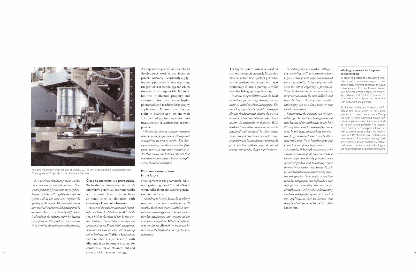
Focusing mechanism and final lens of Sigma7300.The lens is developed in cooperation withCorning Tropel Corporation, who has made the lens.
Working on patents for long-termcompetitiveness
In order to protect the company’s inno-vations and to guarantee long-term com-petitiveness, Micronic conducts an activepatent program. Micronic focuses intenselyon intellectual property rights and encour-ages initiatives that can lead to patents.Thisis done both internally and in cooperationwith customers and partners.
By the end of the year Micronic had 51patent families of which 19 have beengranted in at least one country. Duringthe year Micronic submitted eleven newpatent applications and these are includ-ed in the patent portfolio. The patentscover primary technological solutions aswell as unique constructions and applica-tions. In 2002 Micronic was granted sevennew patents. Most notable among theseare a number of SLM-related US patentsthat protect the important technology inthe next generation of pattern generators.
Reduced workforce in weak market2002 was characterized by a contin-ued weak market which negativelyaffected the propensity to investamong Micronic’s customers. As aresult of falling sales, Micronic tooksteps during the end of the year to cutcosts, including a ten percent reduc-tion in the workforce. Within thegroup, 29 fully employed were affect-ed by the decrease in operations, 22 inSweden while 4 employees in usa and3 employees in Japan were affected.
At the end of 2002 the group had 338employees in Sweden, usa, Japan,Taiwan and China. 259 of the em-ployees in Sweden work at the headoffice in Täby and 10 at the branchoffice in Gothenburg. Taking into consideration the reduction in work-force, that was not at year end comp-letely executed, the total number ofemployees is 318.
All research & development and pro-duction is carried out in Sweden. Thesubsidiaries in usa, Japan and Taiwanfocus primarily on service, customersupport and maintenance of installedsystems. 126 individuals are engagedin research & development, 80 areinvolved with production and instal-lation, and 93 work with marketing,sales and customer support. Microniclargely reflects the multiculturalsociety with employees from severalcountries.
The average age of the employees atMicronic is 37 and the average employ-ment term is about five years. Womenmake up 20 percent of the workforce.
“My everyday work is all about pushing the limits of what is possible, not for the sake of the technology, but for the benefit of our customers. Right now, our main concern is to improve the purity of our optical components to almost unimaginable levels”.Mikael Blomström, mechanical engineer, Sweden
31
Entrepreneurialism andcutting-edge expertise
30
Micronic is a high-tech company thatis constantly facing new technologicalchallenges. This requires a workforcewith solid expertise in order to meetthe customers’ expectations and in-crease the company’s competitiveness.The employees are therefore an impor-tant resource for Micronic and for itsfuture growth. Constantly developingthe skills of the employees is crucial inorder to stay in the front line of tech-nological development.
The employees work independent-ly and have considerable responsibili-ty based on Micronic’s guidelines foroperations. The entrepreneurial spiritthat has permeated the company sincethe start is an important driving force.The sense of unity within the compa-ny is strong as is the desire and moti-vation to take on new challenges.
Micronic works with universitiesand institutes of technology, whichguarantees that the company can main-tain a high level of expertise andattract well-educated, new recruits.The majority of Micronic’s employeeshave academic degrees whereof manyhave a doctor’s degree or hold a licen-tiate.
Opportunities for skills developmentMicronic strongly emphasizes provid-ing its employees with opportunitiesto develop their skills. This enablesthe company to maintain a motivatedworkforce and the cutting edge ex-pertise that has placed Micronic in itsunique position. All of the employeesare given initial training to strength-ening their understanding of the com-pany’s technology and products. Inaddition, the company defines, on anongoing basis, the requirements ofeach team and establishes develop-ment plans accordingly. Skills deve-lopment takes place both internallyand through external training. In2002 the company has focused itsexternal training on strengtheningthe leadership.
An attractive workplaceMicronic attaches great importance tocreating incentives for its employeesto increase their motivation andstrengthen the link between what isbest for the company and what is bestfor the individual. One of Micronic’sexpressed goals is to be an attractiveemployer and to recruit individualswith a high level of expertise in theirrespective fields.
Micronic rewards initiatives taken,for example, by compensating forboth patent applications and awardedpatents.
Micronic’s goal is to offer itsemployees a stimulating workplace.Through the staff club, the employeesare offered a number of activities,including both social activities andopportunities for physical training.
Absence due to illness amounted to2.5 percent in 2002, of which short-term absence accounted for 1.1percent.Women Men Total
Sweden 59 210 269USA 1 17 18Japan 6 40 46Taiwan 1 2 3China 1 1 2
Total 68 270 338
Employees as of December 31, 2002
Employees by function
Production andinstallation 24 %
Research and development
37 %
Marketing,sales and customer support 28 %
Management and support
functions 11%
33
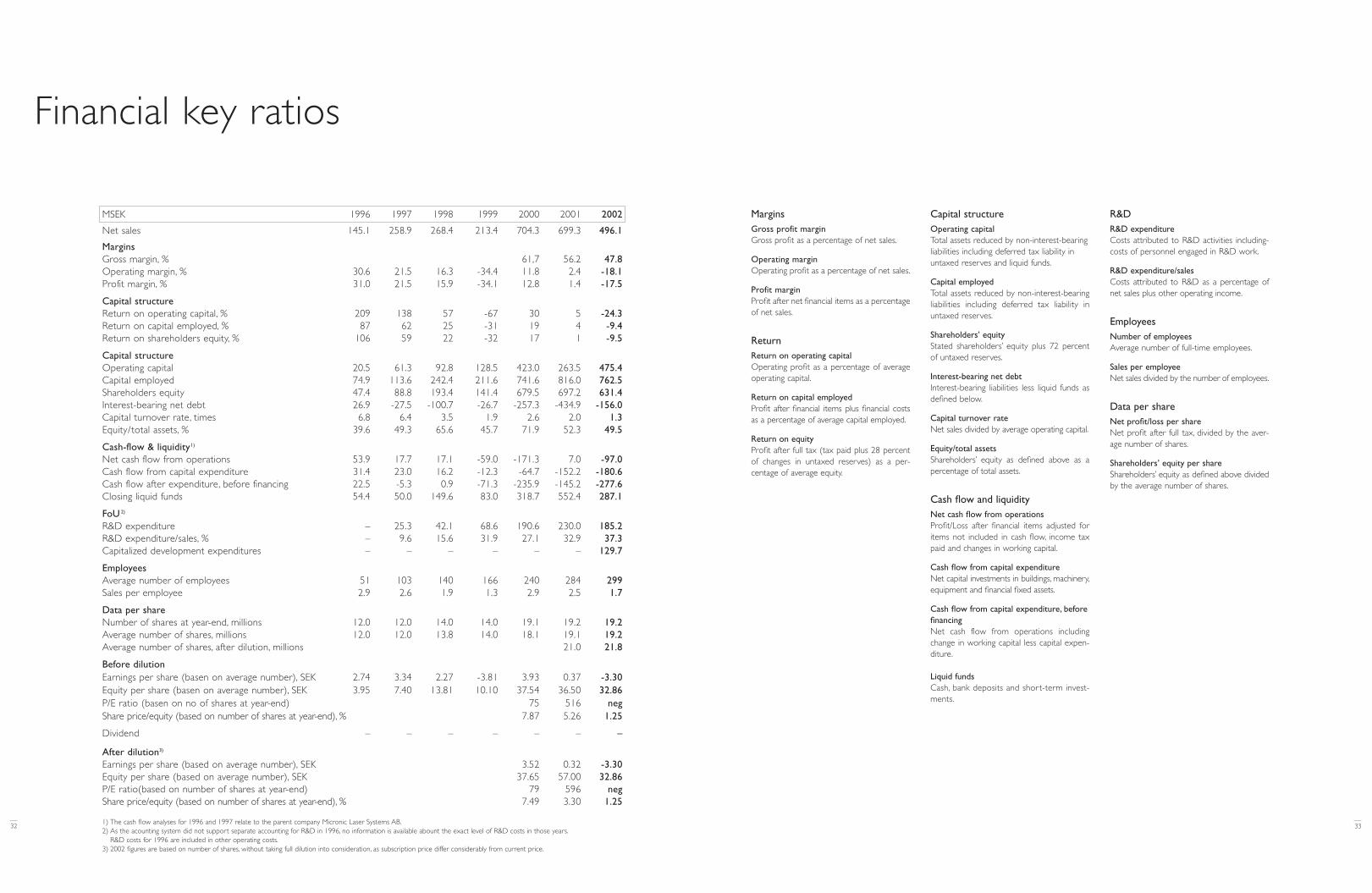
Financial key ratios
321) The cash flow analyses for 1996 and 1997 relate to the parent company Micronic Laser Systems AB.2) As the acounting system did not support separate accounting for R&D in 1996, no information is available abount the exact level of R&D costs in those years.
R&D costs for 1996 are included in other operating costs.3) 2002 figures are based on number of shares, without taking full dilution into consideration, as subscription price differ considerably from current price.
MSEK 1996 1997 1998 1999 2000 2001 2002
Net sales 145.1 258.9 268.4 213.4 704.3 699.3 496.1
MarginsGross margin, % 61,7 56.2 47.8Operating margin, % 30.6 21.5 16.3 -34.4 11.8 2.4 -18.1Profit margin, % 31.0 21.5 15.9 -34.1 12.8 1.4 -17.5
Capital structureReturn on operating capital, % 209 138 57 -67 30 5 -24.3Return on capital employed, % 87 62 25 -31 19 4 -9.4Return on shareholders equity, % 106 59 22 -32 17 1 -9.5
Capital structureOperating capital 20.5 61.3 92.8 128.5 423.0 263.5 475.4Capital employed 74.9 113.6 242.4 211.6 741.6 816.0 762.5Shareholders equity 47.4 88.8 193.4 141.4 679.5 697.2 631.4Interest-bearing net debt 26.9 -27.5 -100.7 -26.7 -257.3 -434.9 -156.0Capital turnover rate, times 6.8 6.4 3.5 1.9 2.6 2.0 1.3Equity/total assets, % 39.6 49.3 65.6 45.7 71.9 52.3 49.5
Cash-flow & liquidity1)
Net cash flow from operations 53.9 17.7 17.1 -59.0 -171.3 7.0 -97.0Cash flow from capital expenditure 31.4 23.0 16.2 -12.3 -64.7 -152.2 -180.6Cash flow after expenditure, before financing 22.5 -5.3 0.9 -71.3 -235.9 -145.2 -277.6Closing liquid funds 54.4 50.0 149.6 83.0 318.7 552.4 287.1
FoU 2)
R&D expenditure – 25.3 42.1 68.6 190.6 230.0 185.2R&D expenditure/sales, % – 9.6 15.6 31.9 27.1 32.9 37.3Capitalized development expenditures – – – – – – 129.7
EmployeesAverage number of employees 51 103 140 166 240 284 299Sales per employee 2.9 2.6 1.9 1.3 2.9 2.5 1.7
Data per shareNumber of shares at year-end, millions 12.0 12.0 14.0 14.0 19.1 19.2 19.2Average number of shares, millions 12.0 12.0 13.8 14.0 18.1 19.1 19.2Average number of shares, after dilution, millions 21.0 21.8
Before dilutionEarnings per share (basen on average number), SEK 2.74 3.34 2.27 -3.81 3.93 0.37 -3.30Equity per share (basen on average number), SEK 3.95 7.40 13.81 10.10 37.54 36.50 32.86P/E ratio (basen on no of shares at year-end) 75 516 negShare price/equity (based on number of shares at year-end), % 7.87 5.26 1.25
Dividend – – – – – – –
After dilution3)
Earnings per share (based on average number), SEK 3.52 0.32 -3.30Equity per share (based on average number), SEK 37.65 57.00 32.86P/E ratio(based on number of shares at year-end) 79 596 negShare price/equity (based on number of shares at year-end), % 7.49 3.30 1.25
MarginsGross profit marginGross profit as a percentage of net sales.
Operating margin Operating profit as a percentage of net sales.
Profit marginProfit after net financial items as a percentageof net sales.
ReturnReturn on operating capitalOperating profit as a percentage of averageoperating capital.
Return on capital employedProfit after financial items plus financial costsas a percentage of average capital employed.
Return on equityProfit after full tax (tax paid plus 28 percentof changes in untaxed reserves) as a per-centage of average equity.
Capital structureOperating capitalTotal assets reduced by non-interest-bearingliabilities including deferred tax liability inuntaxed reserves and liquid funds.
Capital employedTotal assets reduced by non-interest-bearingliabilities including deferred tax liability inuntaxed reserves.
Shareholders’ equityStated shareholders’ equity plus 72 percentof untaxed reserves.
Interest-bearing net debtInterest-bearing liabilities less liquid funds asdefined below.
Capital turnover rateNet sales divided by average operating capital.
Equity/total assetsShareholders’ equity as defined above as apercentage of total assets.
Cash flow and liquidityNet cash flow from operationsProfit/Loss after financial items adjusted foritems not included in cash flow, income taxpaid and changes in working capital.
Cash flow from capital expenditureNet capital investments in buildings, machinery,equipment and financial fixed assets.
Cash flow from capital expenditure, beforefinancingNet cash flow from operations includingchange in working capital less capital expen-diture.
Liquid fundsCash, bank deposits and short-term invest-ments.
R&DR&D expenditureCosts attributed to R&D activities including-costs of personnel engaged in R&D work.
R&D expenditure/salesCosts attributed to R&D as a percentage ofnet sales plus other operating income.
EmployeesNumber of employeesAverage number of full-time employees.
Sales per employeeNet sales divided by the number of employees.
Data per shareNet profit/loss per shareNet profit after full tax, divided by the aver-age number of shares.
Shareholders’ equity per shareShareholders’ equity as defined above dividedby the average number of shares.
Micronic Japan k.k. is a customer sup-port company with local service officesclose to the company’s customers inJapan. Micronic Laser Systems Inc.,offers customer support to customers inthe United States, and reinforces globalmarketing by providing the companywith a higher profile in the us market.Micronic’s operation in Taiwan becamean independent subsidiary as of Octo-ber 1, 2002 and offers customer sup-port. Micronic has also established abranch office in Shanghai to raise thecompany’s profile in China. MicronicTreasury ab serves as an intermediaryfor the distribution of the warrants programs aimed at the company’semployees and partners.
Order intake and order backlog
The order intake in 2002 amounted tomsek 459 (633), a reduction of 27 (-17)percent. The global service businessaccounted for msek 81 (70) of the totalorder intake. In 2002Micronic receivedorders for a total of 8 (10) systems ofwhich 3 (3) systems are for the semi-conductor segment, 2 (5) for the displaysegment and 3 (2) systems for the MultiPurpose segment. The order book atthe end of the year was worth msek 231(279) and is entirely related to systems.All of the systems are expected to bedelivered in 2003.
Invoiced sales
Net sales in 2002 amounted to msek496 (699), a reduction of 29 percent (0).The global service business accountedfor msek 81 (70) of the sales, which isequivalent to 17 (10) percent of thetotal sales. In 2002, 9 (15) systemswere delivered and invoiced, of which1 (2) was an upgrade. Micronic deli-vered 2 (5) systems to the semiconduc-tor market, equivalent to 26 (37) per-cent of the sales. 4 (5) systems weredelivered to the display market, whichis 44 (36) percent of the sales, while 3(5) systems were delivered to the MultiPurpose market, equivalent to 13 (17)percent of the sales for the year.
The global service operation con-tinues to expand as the number of in-stalled systems increases. The totalnumber of employees in Japan, Taiwan,China and the usa increased from 64to 69.
At the end of 2002, Micronic had50 (42) service contracts with cus-tomers around the world and some 90 installed systems.
Operating expenses
Starting in 2002, Micronic is reportingresults by department to more accu-rately reflect the business. The operat-ing expenses for the year amounted tomsek 586 (684). The cost of goods soldamounted to msek 259 (306), whichresulted in a gross margin of 48 (56)percent. The lower gross margin can beexplained by the fact that the firstSigma system was delivered with asomewhat lower gross margin than
other systems and also by the impactof the decreasing dollar effect as allsales are in us dollars. r&d expendi-ture amounting to msek 185 (230) wascharged against the earnings. In addi-tion to this, development expenditurein the amount of msek 130 was capi-talized in accordance with applicableaccounting recommendations andaccounted for as intangible assets.Development expenditures was capi-talized after an individual valuation ofeach development project. Deprecia-tion of capitalized expenditure startswhen the respective projects begin togenerate income. In 2002 deprecationwas initiated on certain projects result-ing in around msek 3 being chargedagainst the earnings. The company’stotal r&d expenditure amounted tomsek 311 (230). msek 35 of the totalr&d expenditure is related to masklesslithography. Such costs are expensed intheir entirety as they are incurred.
The sales costs amounted to msek47 (67) and include commission.Administrative costs include the sub-sidiaries’ operations. Other costs con-sist mainly of the negative effects ofexchange rate differences upon trans-lation of balance sheet items related tooperations to Swedish kronor.
Result
The result after financial items for2002 was negative at msek -87 (9), afall of msek 96. If all developmentcosts had been expensed, this figurewould have been msek -212. Despitethe dramatic fall in sales, the companyhas maintained and even increased itsfocus on r&d. An amount of msek 7 in 35
The Board of Directors and the Presi-dent of Micronic Laser Systems ab(publ.), Co. reg. no. 556351-2374,hereby present the annual report for the 2002 financial year (January 1 –December 31, 2002).
Operations
Micronic Laser Systems is a high-techcompany that develops, manufacturesand markets a series of extremely accu-rate laser pattern generators for the pro-duction of photomasks. The technologyis called microlithography. Micronic’ssystems are used by the world’s leadingelectronics corporations to manufacturetelevision screens, displays for comput-ers and semiconductor components.
Events in 2002
Market conditions
2002 was a weak year. The state of theworld economy combined with lowsales as well as weak development inthe mobile communication market,resulted in a continued weak semi-conductor market. Micronic, as well asother capital equipment suppliers hasexperienced cuts in investments fromthe customers. Despite high sales offlat-panel displays the demand forpattern generators to this industry hasremained stable at the same level as last year. The demand for Micronic’sMulti Purpose systems is tightly connected to demand in the semicon-ductor industry.
Delivery of the first Sigma SystemMicronic delivered its first Sigma system to DuPont Photomasks. TheSigma system, which is based on theslm technology, is expected to have asignificant impact on photomask writ-ing in the semiconductor industry.
Order for a second Sigma System
Micronic received a second order for asystem in the Sigma7000 series for theproduction of advanced photomasksfor the 130 nanometer technology nodeand future nodes.
Introduction of the next generation of Sigma
Micronic introduced Sigma7300,which is for use in volume productionin the 90 and towards 65 nanometertechnology nodes. The system offersstate of the art resolution and can writephotomasks for the critical layers withshort write times to reduce the turn-around time and cut photomask costs.
Launch of the next generation of PDPs
Micronic launched a new laser patterngenerator for the next generation ofplasma display panels (pdps). Micronic’snew system, mp185+, has the capacityto write photomasks up to 1,400 x1,850 mm.
Continued focus on local customer supportMicronic has signed a partnershipagreement with Hermes-Epitek, one ofTaiwan’s leading suppliers to the semi-conductor industry. Hermes is respon-sible for Micronic’s sales and supportactivities in Taiwan and South EastAsia. Micronic has also established abranch office in Shanghai, China.These ventures will enable Micronic tofurther expand its operation in theTaiwanese and South East Asian mar-kets for semiconductors, displays andMulti Purpose products.
Cutbacks to adapt the company to a market in recession
The weak semiconductor market andgreater uncertainty over deliveries tothis segment have forced Micronic totake steps to cut the company’s costs.The overall costs for external consul-tants have been reduced and the num-ber of employees has been cut by closeto ten percent. Restructuring costsamounting to around msek 7 nega-tively affected the year’s result.
The Micronic Group – December 31, 2002
The Group consists of the parent com-pany, Micronic Laser Systems ab, andits wholly-owned subsidiaries MicronicJapan k.k., Micronic Treasury ab,Micronic Laser Systems Inc. andMicronic Laser Systems Far East Ltd.
Report of the Directors
34
Board activitiesThe Board of Directors consists of eightmembers who are elected at the AnnualGeneral Meeting. In 2002 the Boardconvened 19 (14) meetings, of whichseveral were extraordinary Board meet-ings focusing primarily on the compa-ny’s strategic development and the cur-rent market conditions. The Boardworks according to a formal work planin which the division of duties betweenthe Board and the President are stipu-lated. During 2002, a nominationcommittee, consisting of Lars Öjeforsas the chairman and Bert Jeppsson andChrister Zetterberg, have had discus-sions with major shareholders.
After the General Annual Meetinghas been held, The Board intends toinstall an audit committee and a remu-neration committee.
Outlook
The market for equipment to the semi-conductor industry is expected to growby approximately 16 percent in 2003(Gartner Dataquest, December 2002).Gartner estimates the pattern generator
market will grow by around the sameamount. We believe demand in thenear future will be dominated by tech-nology investments. The market ischaracterized by a limited number oflarge orders and this can have a greatimpact on individual companies aswell as on the market as a whole anddepending on when during the yearthese orders are placed.
Micronic has been working inten-sively on developing products for themost advanced photomask segmentwhere demand is expected to be. Thismakes the company well positioned toincrease sales as well as market shareeven if the market conditions of 2002persist.
The display industry is still grow-ing at a high pace, with a yearly growthof between 10 and 30 percent. Micro-nic´s stable position and wide range ofproducts leave it well prepared to meetcustomer demands in the near future aswell as long-term. The market for pat-tern generators is however more strong-ly connected to technology develop-ment of displays rather than to volume
increases. Micronic estimates the de-mand for pattern generators to the dis-play market to be in line with last year’s.
Market development within ourMulti Purpose product line is driven toa large degree by increasing demand foradvanced electronic packaging from thesemiconductor industry. As estimatesfor the semiconductor market now in-dicate a recovery during the second partof 2003, we are carefully optimistic forthe Multi Purpose segment as well.
Proposed disposition of earnings
The consolidated non-restricted equityas stated in the consolidated balancesheet amounts to tsek 48,440(104,808). It is proposed that the parent company’s accumulated loss bedealt with as follows:
37
restructuring costs, as part of effortsinitiated at the end of 2002 to reduceoperations, was charged against theearnings.
Inventories
The inventories amounted to msek328 (279) at the end of the year includ-ing work in progress of msek 182(158) and supplies of msek 146 (121).The item “Work in progress” includesongoing production of systems fordelivery to customers, certain test andtraining systems and systems for customer demonstrations. In 2002,machines to the total value of msek 29that are only used for developmenthave been moved from “Work inprogress” to “Equipment”. Current andaccrued costs for materials and labor forthe completion of planned systems arecharged against work in progress.
Accounts receivable
Accounts receivable amounted tomsek 188 (213) at the end of the year,of which msek 75, or 40 percent, ispayable within three months.
Capital expenditure
Major renovation of and extensions tothe production and office premiseswere completed in 2001. Additionalrenovation work on the property wascarried out in 2002 costing aroundmsek 3. The company also investedmsek 37 in machinery and productionequipment of which msek 23 is leasedequipment. Additional investmentsamounting to msek 10 were made in anew company-wide information sys-tem. Investment on the system began
in 2001 and it is classified as an intan-gible asset. Most of the year’s invest-ments is related to capitalized develop-ment expenditures amounting tomsek 130. The total amount of invest-ments in tangible and intangible assetswas msek 180 (136).
Cash flow, liquid funds and financial position
The Group’s liquid funds at the end ofthe year amounted to msek 287 (552),excluding unutilized overdraft facili-ties. During the year, the liquid fundswas reduced by msek 265 (234). Theequity/assets ratio was 50 (52) percentat the end of the year.
Operations consumed msek 97 included changes in working capital.Investments in tangible and intan-gible fixed assets amounted to msek180 (136).
Currency exposure
Sales are invoiced almost exclusively inus dollars. The company’s policy is tolimit the effects of currency fluctuations.As a result of the great uncertainty in2002 with respect to delivery dates forsystems, the amount of hedging of cur-rency flows was not as extensive as inthe past. At year-end there were no for-ward contracts outstanding.
Currency effects relating to valua-tion of the order intake, invoiced salesand the order book are dealt withaccording to the following principles.The order intake and invoiced sales arestated at the respective spot rate. Theclosing balance of the order book is val-ued at the closing day rates, taking intoaccount the hedging contracts that arein place.
Currency differences of an operatingnature, a negative net of msek -16,have been included in the operatingresult, while positive currency diffe-rences of a financial nature, amountingto msek 0.3, have been included infinancial costs and income.
Research and development
r&d expenditure amounted to msek311 (230) in 2002. msek 185 of thisamount was expensed as the cost wasincurred, while msek 130 was capital-ized. The focus in 2002 has been ondeveloping the slm technology withinthe semiconductor segment. The in-crease including changes in workingcapital compared to the previous yearis mainly related to extended partner-ship agreements and the use of exter-nal consultants.
Organization
The operations are based on a line/project-based organization with de-fined areas of responsibility for market-ing, sales, strategic development, coredevelopment, system applications,production & installation, customersupport and finance & administration.At the end of the year, the number ofemployees was 338 (327). Taking intoaccount the reduction in operations,which was not entirely complete at theend of 2002, the number of employeesis actually 318. The reduction of staffwas around ten percent, from 355at theend of the third quarter.
36
2002
Retained earnings 99,477,828Net loss for the year -148,154,747
-48,676,919
Proposed disposition of loss
To be carried forward -48,676,919
Total -48,676,919
Täby, February 11, 2003
Bert Jeppsson Millert Carlsson Sven LöfquistChairman President
Hans Fletcher Göran Malm Magnus Ryde Christer Zetterberg Lars Öjefors
Our audit report was submitted on February 11, 2003.
Anders Östberg Per FridolinAuthorized Public Accountant Authorized Public AccountantLindebergs Grant Thornton AB Lindebergs Grant Thornton AB
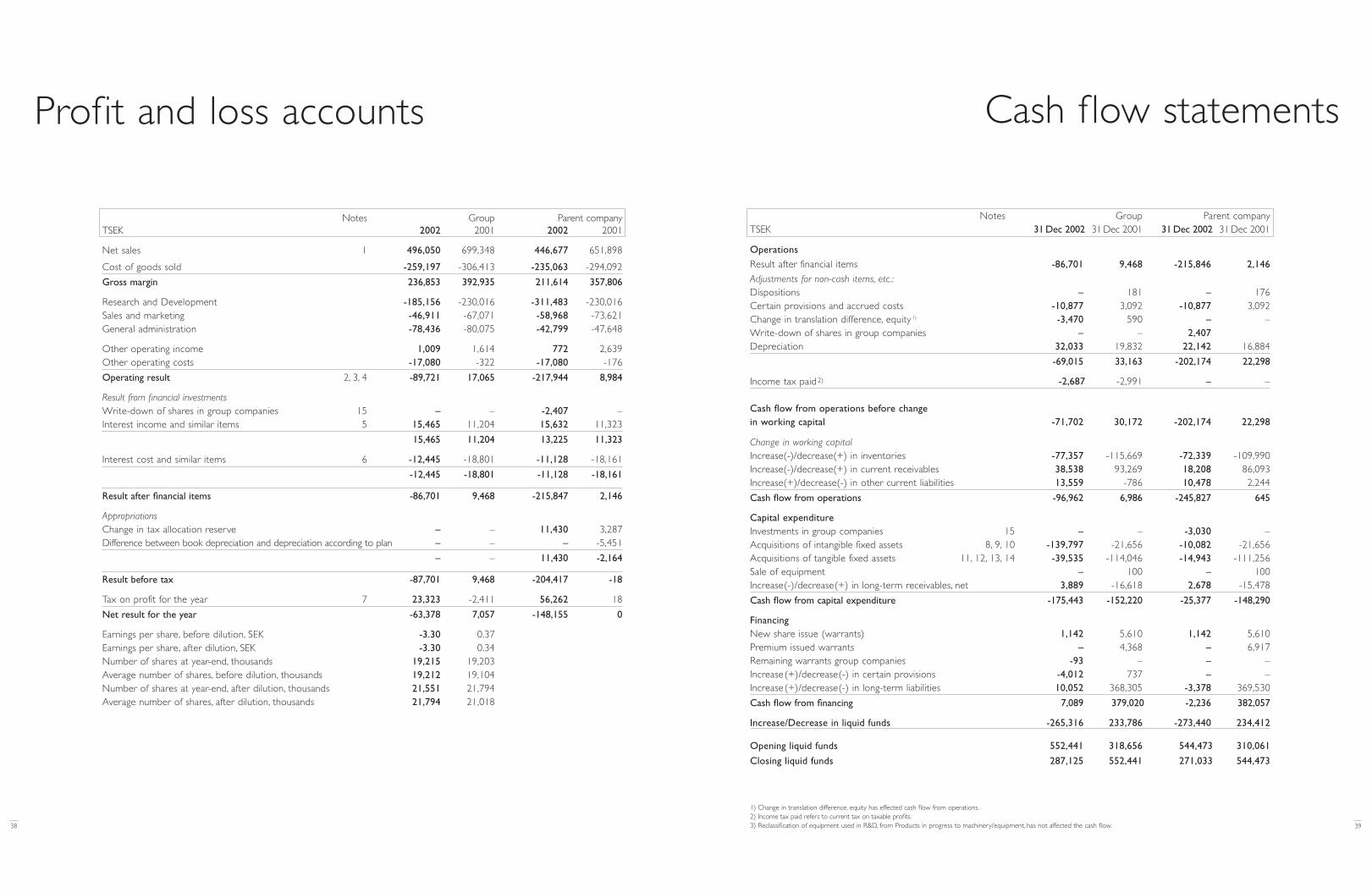
Cash f low statements
39
Profit and loss accounts
38
Notes Group Parent companyTSEK 31 Dec 2002 31 Dec 2001 31 Dec 2002 31 Dec 2001
Operations
Result after financial items -86,701 9,468 -215,846 2,146
Adjustments for non-cash items, etc.:Dispositions – 181 – 176Certain provisions and accrued costs -10,877 3,092 -10,877 3,092Change in translation difference, equity 1) -3,470 590 – –Write-down of shares in group companies – – 2,407Depreciation 32,033 19,832 22,142 16,884
-69,015 33,163 -202,174 22,298
Income tax paid 2) -2,687 -2,991 – –
Cash flow from operations before changein working capital -71,702 30,172 -202,174 22,298
Change in working capitalIncrease(-)/decrease(+) in inventories -77,357 -115,669 -72,339 -109,990Increase(-)/decrease(+) in current receivables 38,538 93,269 18,208 86,093Increase(+)/decrease(-) in other current liabilities 13,559 -786 10,478 2,244
Cash flow from operations -96,962 6,986 -245,827 645
Capital expenditureInvestments in group companies 15 – – -3,030 –Acquisitions of intangible fixed assets 8, 9, 10 -139,797 -21,656 -10,082 -21,656Acquisitions of tangible fixed assets 11, 12, 13, 14 -39,535 -114,046 -14,943 -111,256Sale of equipment – 100 – 100Increase(-)/decrease(+) in long-term receivables, net 3,889 -16,618 2,678 -15,478
Cash flow from capital expenditure -175,443 -152,220 -25,377 -148,290
FinancingNew share issue (warrants) 1,142 5,610 1,142 5,610Premium issued warrants – 4,368 – 6,917Remaining warrants group companies -93 – – –Increase(+)/decrease(-) in certain provisions -4,012 737 – –Increase(+)/decrease(-) in long-term liabilities 10,052 368,305 -3,378 369,530
Cash flow from financing 7,089 379,020 -2,236 382,057
Increase/Decrease in liquid funds -265,316 233,786 -273,440 234,412
Opening liquid funds 552,441 318,656 544,473 310,061
Closing liquid funds 287,125 552,441 271,033 544,473
Notes Group Parent companyTSEK 2002 2001 2002 2001
Net sales 1 496,050 699,348 446,677 651,898
Cost of goods sold -259,197 -306,413 -235,063 -294,092
Gross margin 236,853 392,935 211,614 357,806
Research and Development -185,156 -230,016 -311,483 -230,016Sales and marketing -46,911 -67,071 -58,968 -73,621General administration -78,436 -80,075 -42,799 -47,648
Other operating income 1,009 1,614 772 2,639Other operating costs -17,080 -322 -17,080 -176
Operating result 2, 3, 4 -89,721 17,065 -217,944 8,984
Result from financial investmentsWrite-down of shares in group companies 15 – – -2,407 –Interest income and similar items 5 15,465 11,204 15,632 11,323
15,465 11,204 13,225 11,323
Interest cost and similar items 6 -12,445 -18,801 -11,128 -18,161
-12,445 -18,801 -11,128 -18,161
Result after financial items -86,701 9,468 -215,847 2,146
AppropriationsChange in tax allocation reserve – – 11,430 3,287Difference between book depreciation and depreciation according to plan – – – -5,451
– – 11,430 -2,164
Result before tax -87,701 9,468 -204,417 -18
Tax on profit for the year 7 23,323 -2,411 56,262 18
Net result for the year -63,378 7,057 -148,155 0
Earnings per share, before dilution, SEK -3.30 0.37Earnings per share, after dilution, SEK -3.30 0.34Number of shares at year-end, thousands 19,215 19,203Average number of shares, before dilution, thousands 19,212 19,104Number of shares at year-end, after dilution, thousands 21,551 21,794Average number of shares, after dilution, thousands 21,794 21,018
1) Change in translation difference, equity has effected cash flow from operations.2) Income tax paid refers to current tax on taxable profits.3) Reclassification of equipment used in R&D, from Products in progress to machinery/equipment, has not affected the cash flow.
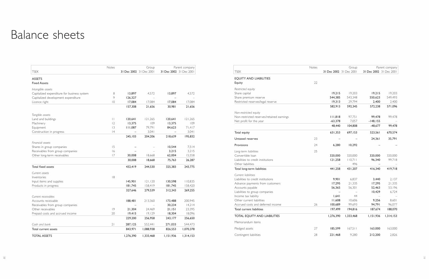
41
Balance sheets
40
Notes Group Parent companyTSEK 31 Dec 2002 31 Dec 2001 31 Dec 2002 31 Dec 2001
EQUITY AND LIABILITIESEquity 22
Restricted equityShare capital 19,215 19,203 19,215 19,203Share premium reserve 544,385 543,348 550,623 549,493Restricted reserves/legal reserve 19,313 29,794 2,400 2,400
582,913 592,345 572,238 571,096
Non-restricted equityNon-restricted reserves/retained earnings 111,818 97,751 99,478 99,478Net profit for the year -63,378 7,057 -148,155 –
48,440 104,808 -48,677 99,478
Total equity 631,353 697,153 523,561 670,574
Untaxed reserves 23 – – 24,361 35,791
Provisions 24 6,280 10,292 – –
Long-term liabilities 25Convertible loan 320,000 320,000 320,000 320,000Liabilities to credit institutions 121,258 110,711 96,340 99,718Other liabilities – 496 – –
Total long-term liabilities 441,258 431,207 416,340 419,718
Current liabilitiesLiabilities to credit institutions 9,901 6,837 3,440 2,137Advance payments from customers 17,295 21,335 17,295 21,335Accounts payable 56,365 56,301 52,463 53,196Liabilities to group companies – – 10,429 6,724Income tax liability 1,641 44 – –Other current liabilities 11,608 10,606 9,256 8,601Accrued costs and deferred income 26 100,689 99,693 94,791 96,077
Total current liabilities 197,499 194,816 187,674 188,070
TOTAL EQUITY AND LIABILITIES 1,276,390 1,333,468 1,151,936 1,314,153
Memorandum items
Pledged assets 27 185,599 167,511 163,000 163,000
Contingent liabilities 28 221,468 9,280 212,200 2,826
Notes Group Parent companyTSEK 31 Dec 2002 31 Dec 2001 31 Dec 2002 31 Dec 2001
ASSETSFixed Assets
Intangible assetsCapitalized expenditure for business system 8 13,897 4,572 13,897 4,572Capitalized development expenditure 9 126,327 – – –Licence right 10 17,084 17,084 17,084 17,084
157,308 21,656 30,981 21,656
Tangible assetsLand and buildings 11 120,641 121,265 120,641 121,265Machinery 12 13,375 109 13,375 109Equipment 13 111,087 79,791 84,623 71,417Construction in progress 14 – 3,041 – 3,041
245,103 204,206 218,639 195,832
Financial assetsShares in group companies 15 – – 10,544 7,514Receivables from group companies 16 – – 3,215 3,215Other long-term receivables 17 30,008 18,668 62,004 15,558
30,008 18,668 75,763 26,287
Total fixed assets 432,419 244,530 325,383 243,775
Current assetsInventories 18Input items and supplies 145,901 121,120 130,598 110,835Products in progress 181,745 158,419 181,745 158,420
327,646 279,539 312,343 269,255
Current receivablesAccounts receivable 188,481 213,360 173,488 200,945Receivables from group companies – – 30,234 14,214Other receivables 19 21,304 24,469 21,151 23,395Prepaid costs and accrued income 20 19,415 19,129 18,304 18,096
229,200 256,958 243,177 256,650
Cash and bank 21 287,125 552,441 271,033 544,473
Total current assets 843,971 1,088,938 826,553 1,070,378
TOTAL ASSETS 1,276,390 1,333,468 1,151,936 1,314,153
currencies are valued at closing dayrates, except for the parent company’slong-term claims on foreign subsidi-aries, which are valued at the rates thatwere valid when the claims arose.
Currency differences on operatingreceivables and payables is presented inthe operating result, the net accountedfor either as Other operating income orOther operating costs.
The difference between hedgingrates and daily rates in connectionwith the extension of forward con-tracts is distributed over the durationof the contract. The net effect of hedg-ing premiums is stated under eitherInterest income and similar items orInterest costs and similar items.
Currency differences on operatingincome for the financial year affectedthe operating result negatively bytsek -16,722 (617) and the resultfrom financial investments positivelyby tsek 257 (-13,971).
Inventories
Inventories are valued at the lower of theacquisition value or actual value. Semi-manufactured and finished productshave been valued at direct manufactur-ing cost, including a reasonable amountof indirect costs, taking into accountthe company’s adjusted product lines.
Receivables
Receivables, after individual valuation,have been entered according to the a-mounts that are expected to be received.
Reporting of tax
Current tax refers to the tax that is cal-culated on the basis of the taxable
profit for the year. Deferred tax refers tothe tax that is calculated partly on thebasis of taxable temporary differencesand partly on tax-related deficit. Cur-rent tax requires immediate payment,unlike deferred tax. Group: Deferred taxliabilities/tax claimsare calculated on thebasis of untaxed reserves, intra-groupprofit in inventory, exchange rate prof-its on long-term receivables from for-eign subsidiaries and the parent compa-ny’s expensed development expendi-ture which is capitalized in the Group,and they are stated under Provision/otherlong-term receivables in the balance sheet.Deferred tax expense and deferred taxrevenue are calculated on the basis ofchanges in untaxed reserves, intra-group profit in inventory and develop-ment costs that are expensed in the par-ent company but capitalized in thegroup and are stated under Tax on profitfor the year in the Profit and lossaccounts. Parent company: Deferred taxliabilities are stated as a part of untaxedreserves (i.e. only in the note relating tothe balance-sheet item). Deferred taxexpense is calculated on the basis ofchanges in untaxed reserves and is stat-ed only in the notes to the Profit and lossaccounts as part of the note relating toTax on profit for the year.
Deferred tax claims and Deferred taxrevenue are calculated on the basis of thepart of the year’s tax-related deficit thatis expected to be used against futuretaxable surplus. The receivable is treat-ed either as long and/or short term,depending on when in the future thedeficit is expected to be utilized, i.e.stated under either Other long-term receiv-ables or Other current receivables in the
balance sheet. Tax revenue is stated asTax on profit for the year in the Profit andloss accounts.
Research and development
Costs related to research are expensedas they occur.
From January 1, 2002 an individualvaluation is made of all developmentprojects in accordance with currentaccounting recommendations, and partof the development expenditure is cap-italized and stated as Intangible assets.The assets are depreciated to reflect howthe assets’ value for the company is con-sumed. Depreciation starts when in-come is first generated by the develop-ment project and is spread over thenumber of systems expected to be sold.In 2002, development expenditureamounting to tsek 129,715 was capi-talized. Depreciation on completedprojects amounted to tsek 3,388 in2002. Other development expenditureand costs for research have been ex-pensed as they occur.
Pensions
Pension commitments are normallymanaged through the payment ofinsurance premiums. In foreign sub-sidiaries, provisions are also made forfuture pension commitments for com-pany employees.
Income recognition
Income from systems is recognizedupon delivery. Estimated further costsare taken into account. Payments dueunder service agreements are invoicedin advance and are distributed overthe term of the agreement. 43
The annual report is prepared inaccordance with the recommenda-tions issued by the Swedish FinancialAccounting Standards Council.
There have been no changes in theaccounting principles compared to lastyear. As per January 1, 2002, the recom-mendation rr15, Intangible assets, is-sued by the Swedish Financial Account-ing Standards Council came into effect.
The profit and loss accounts are pre-sented by function which is new for thisyear. The change has been made to givea more fair view of the operations.Some adjustments have been made tothe functional profit and loss accountfor 2001 in comparison to those pre-sented in quarterly reports earlier. Theadjustments have been made to becompareble to 2002. The adjustmentsrelate to the allocation of overhead costs.
Principles of consolidation
The consolidated financial statementsare prepared using the purchase methodand include all subsidiaries.
Translation of financial statementsof foreign subsidiaries
The foreign subsidiaries are regardedas independent foreign companies andvalues are translated using the currentmethod. In 2002 the operation inTaiwan became a subsidiary and hasbeen treated as such since October 1.Assets and liabilities are translated atclosing day exchange rates, while re-venue and costs are translated atapproximate transaction day rates. Anytranslation differences that arise aretaken directly to equity.
Long-term foreign subsidiary recei-vables have been valued at the rate ofexchange at the time the receivablesoriginated. The translation differencefor these receivables has been takendirectly to restricted equity in theconsolidated balance sheets.
Accumulated currency differencesstated directly against equity amountedto tsek 8,738 at the beginning of theyear, and to tsek 5,268 at year-end.The decrease is largely attributable tothe changes in foreign exchange rates.
Intangible and tangible fixed assetsCapitalized expenditure for develop-ment costs, business systems, licenseright, buildings, machinery and equip-ment are stated at their acquisitionvalue after deducting accumulateddepreciation. Intangible and tangiblefixed assets are depreciated on a straight-line basis based on their estimatedperiod of use from the completion orpurchase month. The following depre-ciation rates have been used:
Depreciation of capitalized develop-ment expenditure begins when incomeis first generated by the individual de-velopment project. After an individualvaluation of each development project,the expenditure is depreciated to reflecthow the assets’ value is successively con-sumed, spread out over the number of
systems expected to be sold, but at themost over a five-year period. Depreci-ation of the license right will start whenincome is first generated, which isexpected to be in 2003 at the earliest.The license right will be depreciated toreflect how the assets’ value for the com-pany is successively consumed, at themost over a five year period.
Leasing
Leased assets refer in part to financialleasing and in part to operational leas-ing. Leased assets are stated in the con-solidated balance sheet as fixed assetsand are depreciated in accordance withthe principles for Tangible fixed assetsin general. Future leasing fees arereported as liabilities. Current leasingfees, after deductions for interest, re-duce the amount of the stated liability.
Currency management
Sales are invoiced almost entirely inus dollars.
To control the parent company’scurrency exposure, the company has ahedging policy, according to whichthe net flow in foreign currency, aswell as orders received, are to be par-tially hedged.
The balance sheet items subject tocurrency hedging are Accounts receiv-able, Cash and bank, and Accounts pay-able. Due to a greater amount of un-certainty regarding times of deliveryduring the latter part of 2002, thecompany refrained from going intonew forward contracts as old ones haveexpired. At year-end there were no for-ward contracts outstanding.
Receivables and liabilities in foreign
Accounting principles
42
Buildings 33 yearsCleanroom premises 20 yearsLand improvements 20 yearsCapitalized development expenditure 5 yearsLicense right 5 yearsMachinery and equipment 5 yearsCapitalized expenditurefor business systems 3 yearsComputer equipment 3 years
Not 4 Depreciation per function
Group Parent company2002 2001 2002 2001
Costs for goods sold 11,489 6,724 5,501 4,309R&D 14,448 11,513 14,742 11,513Capitalized development expenditures 3,388 – – –Sales 1,056 1,004 1,056 1,004General administration 1,607 590 844 57
31,988 19,831 22,143 16,883
Note 5 Interest income and similar items
Group Parent company2002 2001 2002 2001
Interest income 12,500 11,204 12,473 11,092Interest income group companies – – 194 231Currency profits 2,965 – 2,965 –
15,465 11,204 15,632 11,323
Note 6 Interest cost and similar items
Group Parent company2002 2001 2002 2001
Interest cost 8,206 3,650 6,889 3,009Currency losses 2,707 13,971 2,707 13,971Other 1,532 1,180 1,532 1,180
12,445 18,801 11,128 18,161
4544
NotesAll amounts in the notes below are in TSEK, except where otherwisestated.
Note 1 Net sales
Group Parent company2002 2001 2002 2001
Europe 5,626 1,675 5,626 1,675USA 132,292 114,388 123,109 108,936Asia 358,132 583,285 317,942 541,287
Total 496,050 699,348 446,677 651,898
Inter-company transactions
10 (8) per cent of the year’s purchases have been from Micronic JapanK.K and Micronic Laser Systems, Inc. 4 (2) per cent of the year’s salehave been to Micronic Japan K.K and Micronic Laser Systems, Inc.
Note 2 Other external costs
Group Parent company2002 2001 2002 2001
Auditing fees and other fees:
Auditing assignments 1,584 899 1,295 597Other assignments 379 996 242 717
“Audit assignments” includes the auditing of the financial statements, theaccounts, the administration of the Board of Directors and president and other such duties that befall the company’s auditors, and advice orother assistance resulting from observation made during the audit or fromthe carrying out of all other such duties. Everything else is considered“Other assignments”.
cont. Note 3 Personnel costs
Other employees 165,603 156,383 117,991 117,028thereof Japan (24,162) (17,011) (–) (–)thereof China (47) (–) (47) (–)thereof Taiwan (1,990) (2,080) (1,617) (2,080)thereof USA (23,077) (22,343) (–) (–)
175,444 163,946 122,749 121,133
Statutory and contractual social security and other contributionsPension insurance premiums –Board and President 346 1,354 276 1,106
thereof Japan (–) (–) (–) (–)thereof China (–) (–) (–) (–)thereof Taiwan (–) (–) (–) (–)thereof USA (70) (248) (–) (–)
Pension insurance premiums –other employees 15,488 14,093 13,699 12,004
thereof Japan (1,223) (597) (–) (–)thereof China (6) (–) (6) (–)thereof Taiwan (105) (48) (97) (48)thereof USA (558) (1,647) (–) (–)
Övriga sociala kostnader 47,101 45,268 43,552 43,577thereof Japan (2,184) (1,692) (–) (–)thereof China (–) (–) (–) (–)thereof Taiwan (152) (87) (143) (87)thereof USA (1,356) (–) (–) (–)
62,935 59,361 57,527 55,581
Board fee
The approved fee for 2002 amounts to TSEK 1,200. No fees are paid tothe boards of subsidiary companies.
Members of the Board
Since March 2001, Bert Jeppon is contracted as working chairman of theBoard, for which he is paid a monthly compensation. From January untilMarch 2002, the monthly compensation was SEK 90,000 and thereafterand until October SEK 45,000. From November 1, Bert Jeppsson is tem-porarily working full time and therefore the monthly compensation isSEK 279,200.The total compensation amounted in 2002 to SEK 1,143,400.As Chairman of the Board, Bert Jeppsson also raises a remuneration ofSEK 300,000 for 2002.
Other members of the Board, except for the President, is entitled toa remuneration of SEK 150,000 for 2002. Millert Carlsson is also workingas a legal counseler for Micronic.The company in which he is working,Law-firm Lindh, Stabell Horten KB, has invoiced SEK 421,816 for con-tinues legal counselling.
There are no pension commitments in respect of the Board.
President
Sven Löfquist was appointed president on March 13, 2001. His contractof employment runs with six months’ mutual notice of termination.Under certain circumstances, Sven Löfquist is entitled to 24 months’severance pay. Löfquist is entitled to monthly compensation amountingto SEK 187,500, in the form of salary and/or the payment of an occu-pational pension premium to an insurance company, at his own discre-tion. Bonus agreements are established for the Executive Managementon a yearly basis.There has been no bonus for 2002.There are no pen-sion commitments in respect of the president.
cont. Note 3 Personnel costs
For 2002, paid salaries and other remunerations and pension insurancepremiums regarding the President amounts to (TSEK):
Monthly compensation, including travel allowances 2,113Benefits of for example car and home computer 60Pension insurance premiums 277Other insurances premiums 30
2,480
Executive Management
For the company’s CFO the contract of employment runs with sixmonths mutual notice of termination.The CFO is entitled to six months’severance pay in a case of notice. Under certain circumstances theCFO, CTO, VP marketing and VP Customer Operation are entitled toseverance pay of 18 months’ salary in the event of their own resignation.Bonus agreements are established for the Executive Management on ayearly basis.There has been no bonus for 2002.
For 2002, paid salaries and other remunerations and pension insurancepremiums regarding the Executive Management (see page 53), exceptthe President, amounts to (TSEK):
Monthly compensation, including travel allowances 6,009Benefits of for example car and home computer 120Pension insurance premiums 631
6,760
Note 3 Personnel costs
Group Parent company2002 2001 2002 2001
Average number of employeesWomen 54 47 44 41
thereof Japan (6) (4) (–) (–)thereof China (1) (–) (1) (–)thereof Taiwan (1) (–) (–) (–)thereof USA (3) (2) (–) (–)
Men 245 237 186 189thereof Japan (34) (26) (–) (–)thereof China (–) (–) (–) (–)thereof Taiwan (3) (5) (–) (5)thereof USA (20) (17) (–) (–)
Total for the company 299 284 230 230
Salaries and other remunerationBoard and president 1) 9,841 7,563 4,758 4,105
thereof Japan (1,608) (447) (–) (–)thereof China (–) (–) (–) (–)thereof Taiwan (–) (–) (–) (–)thereof USA (3,475) (3,012) (–) (–)
Note 7 Tax on results for the year
Group Parent company2002 2001 2002 2001
Current tax expense on profit before tax -2,226 -5,306 – -601Current tax expense/revenue on non-deductible/non-taxable items, etc. -462 2,315 – 601Deferred tax expense taxable loss for last year -3,641 -3,623 -3,641 -3,623Deferred tax revenue on taxable loss for the year 60,488 3,788 59,903 3,641Deferred tax revenue/expense on changes in untaxed reserves 3,200 -606 – –Deferred tax revenue on changes in intra-group profit in inventories 1,125 911 – –Deferred tax expense on capitalized development expenditures -36,320 – – –Deferred tax revenue on depreciation on capitalized development expenditures 949 – – –Deferred tax revenue on temporary differencies, etc. 210 110 – –
23,323 -2,411 56,262 18
Deferred tax revenue on changes in untaxed reserves – – 3,200 -606
Note 8 Capitalized expenditure for business system
Group Parent company31Dec 2002 31Dec 2001 31Dec 2002 31Dec 2001
Opening balance acquisition value 4,572 – 4,572 –
Purchases 10,082 4,572 10,082 4,572
Closing balance accumulated acquisition value 14,654 4,572 14,654 4,572
Opening balance depreciation – – – –Depreciation for the year -757 – -757 –
Closing balance accumulated depreciation -757 – -757 –
Residual value according to plan 13,897 4,572 13,897 4,572
This investment refers to accrued expenses for adjustments and implementation of new fully integrated business information system. Depreciationstarted when the system was fully implemented and running, during the fourt quarter in 2002.
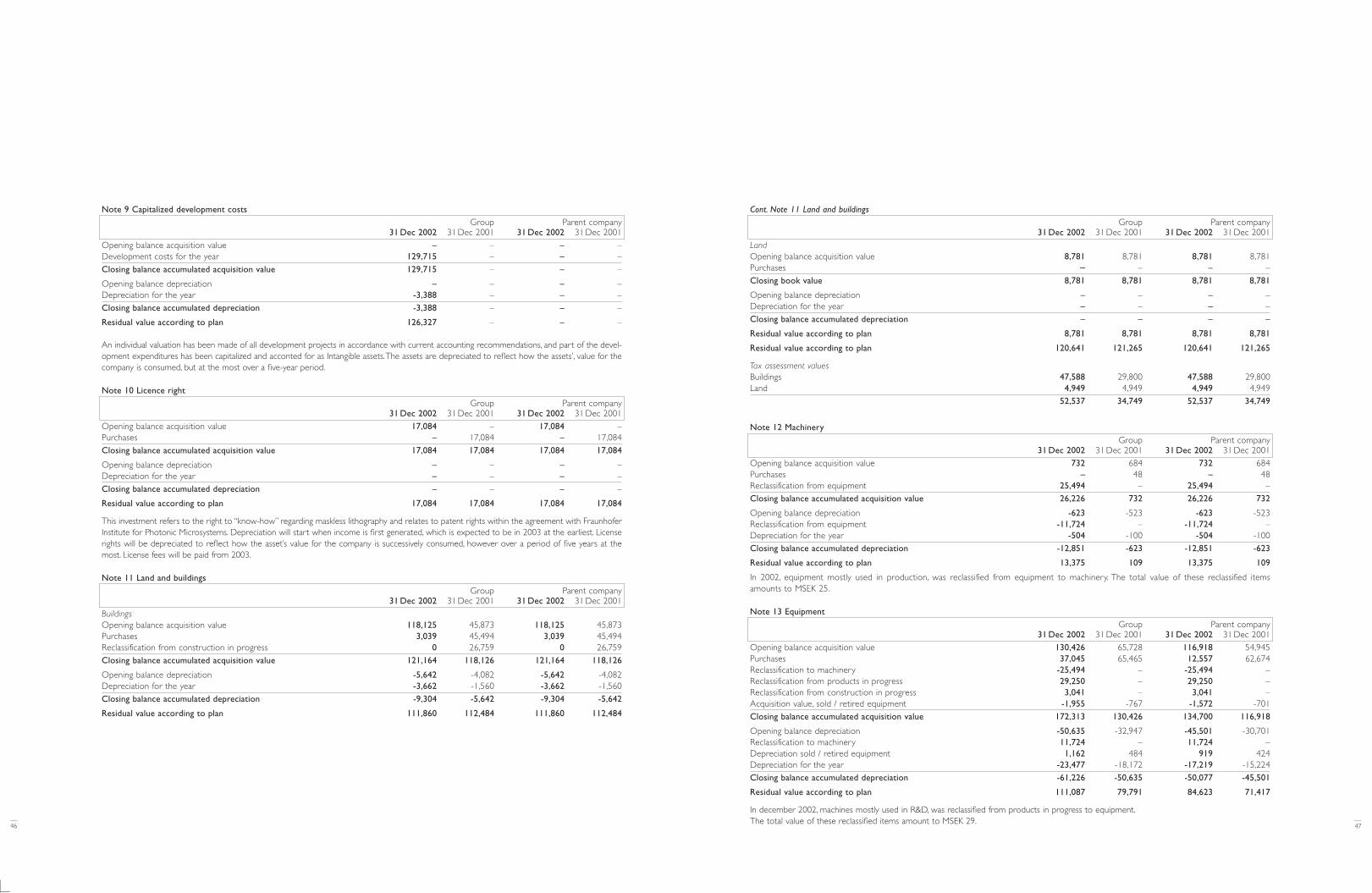
4746
Note 9 Capitalized development costs
Group Parent company31 Dec 2002 31 Dec 2001 31 Dec 2002 31 Dec 2001
Opening balance acquisition value – – – –Development costs for the year 129,715 – – –
Closing balance accumulated acquisition value 129,715 – – –
Opening balance depreciation – – – –Depreciation for the year -3,388 – – –
Closing balance accumulated depreciation -3,388 – – –
Residual value according to plan 126,327 – – –
An individual valuation has been made of all development projects in accordance with current accounting recommendations, and part of the devel-opment expenditures has been capitalized and acconted for as Intangible assets.The assets are depreciated to reflect how the assets’, value for thecompany is consumed, but at the most over a five-year period.
Note 10 Licence right
Group Parent company31 Dec 2002 31 Dec 2001 31 Dec 2002 31 Dec 2001
Opening balance acquisition value 17,084 – 17,084 –Purchases – 17,084 – 17,084
Closing balance accumulated acquisition value 17,084 17,084 17,084 17,084
Opening balance depreciation – – – –Depreciation for the year – – – –
Closing balance accumulated depreciation – – – –
Residual value according to plan 17,084 17,084 17,084 17,084
This investment refers to the right to “know-how” regarding maskless lithography and relates to patent rights within the agreement with FraunhoferInstitute for Photonic Microsystems. Depreciation will start when income is first generated, which is expected to be in 2003 at the earliest. Licenserights will be depreciated to reflect how the asset’s value for the company is successively consumed, however over a period of five years at themost. License fees will be paid from 2003.
Note 11 Land and buildings
Group Parent company31 Dec 2002 31 Dec 2001 31 Dec 2002 31 Dec 2001
BuildingsOpening balance acquisition value 118,125 45,873 118,125 45,873Purchases 3,039 45,494 3,039 45,494Reclassification from construction in progress 0 26,759 0 26,759
Closing balance accumulated acquisition value 121,164 118,126 121,164 118,126
Opening balance depreciation -5,642 -4,082 -5,642 -4,082Depreciation for the year -3,662 -1,560 -3,662 -1,560
Closing balance accumulated depreciation -9,304 -5,642 -9,304 -5,642
Residual value according to plan 111,860 112,484 111,860 112,484
Cont. Note 11 Land and buildings
Group Parent company31 Dec 2002 31 Dec 2001 31 Dec 2002 31 Dec 2001
LandOpening balance acquisition value 8,781 8,781 8,781 8,781Purchases – – – –
Closing book value 8,781 8,781 8,781 8,781
Opening balance depreciation – – – –Depreciation for the year – – – –
Closing balance accumulated depreciation – – – –
Residual value according to plan 8,781 8,781 8,781 8,781
Residual value according to plan 120,641 121,265 120,641 121,265
Tax assessment valuesBuildings 47,588 29,800 47,588 29,800Land 4,949 4,949 4,949 4,949
52,537 34,749 52,537 34,749
Note 12 Machinery
Group Parent company31 Dec 2002 31 Dec 2001 31 Dec 2002 31 Dec 2001
Opening balance acquisition value 732 684 732 684Purchases – 48 – 48Reclassification from equipment 25,494 – 25,494 –
Closing balance accumulated acquisition value 26,226 732 26,226 732
Opening balance depreciation -623 -523 -623 -523Reclassification from equipment -11,724 – -11,724 –Depreciation for the year -504 -100 -504 -100
Closing balance accumulated depreciation -12,851 -623 -12,851 -623
Residual value according to plan 13,375 109 13,375 109
In 2002, equipment mostly used in production, was reclassified from equipment to machinery. The total value of these reclassified items amounts to MSEK 25.
Note 13 Equipment
Group Parent company31 Dec 2002 31 Dec 2001 31 Dec 2002 31 Dec 2001
Opening balance acquisition value 130,426 65,728 116,918 54,945Purchases 37,045 65,465 12,557 62,674Reclassification to machinery -25,494 – -25,494 –Reclassification from products in progress 29,250 – 29,250 –Reclassification from construction in progress 3,041 – 3,041 –Acquisition value, sold / retired equipment -1,955 -767 -1,572 -701
Closing balance accumulated acquisition value 172,313 130,426 134,700 116,918
Opening balance depreciation -50,635 -32,947 -45,501 -30,701Reclassification to machinery 11,724 – 11,724 –Depreciation sold / retired equipment 1,162 484 919 424Depreciation for the year -23,477 -18,172 -17,219 -15,224
Closing balance accumulated depreciation -61,226 -50,635 -50,077 -45,501
Residual value according to plan 111,087 79,791 84,623 71,417
In december 2002, machines mostly used in R&D, was reclassified from products in progress to equipment.The total value of these reclassified items amount to MSEK 29.
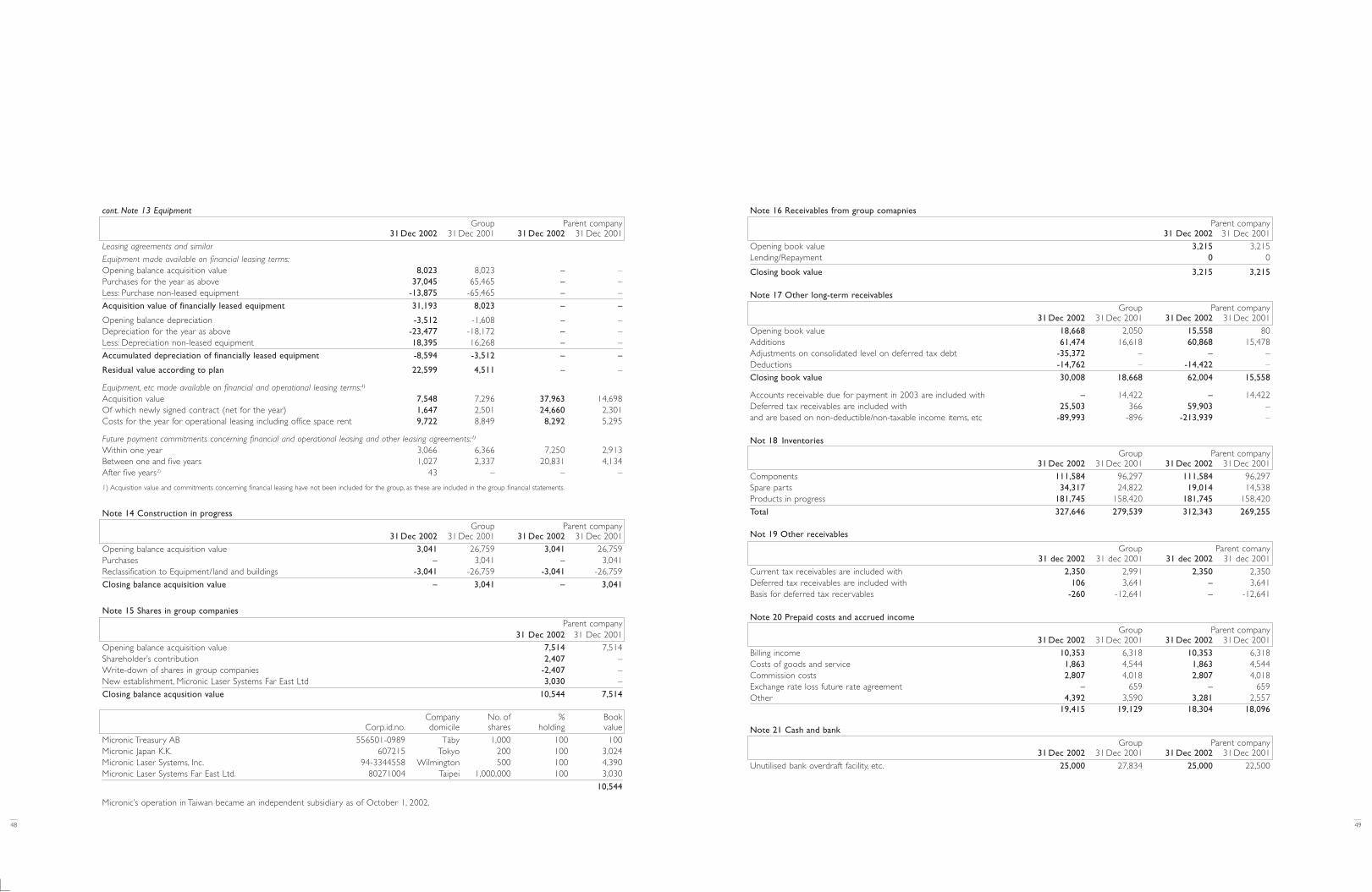
4948
cont. Note 13 Equipment
Group Parent company31 Dec 2002 31 Dec 2001 31 Dec 2002 31 Dec 2001
Leasing agreements and similar
Equipment made available on financial leasing terms:Opening balance acquisition value 8,023 8,023 – –Purchases for the year as above 37,045 65,465 – –Less: Purchase non-leased equipment -13,875 -65,465 – –
Acquisition value of financially leased equipment 31,193 8,023 – –
Opening balance depreciation -3,512 -1,608 – –Depreciation for the year as above -23,477 -18,172 – –Less: Depreciation non-leased equipment 18,395 16,268 – –
Accumulated depreciation of financially leased equipment -8,594 -3,512 – –
Residual value according to plan 22,599 4,511 – –
Equipment, etc made available on financial and operational leasing terms:1)
Acquisition value 7,548 7,296 37,963 14,698Of which newly signed contract (net for the year) 1,647 2,501 24,660 2,301Costs for the year for operational leasing including office space rent 9,722 8,849 8,292 5,295
Future payment commitments concerning financial and operational leasing and other leasing agreements:1)
Within one year 3,066 6,366 7,250 2,913Between one and five years 1,027 2,337 20,831 4,134After five years2) 43 – – –
1) Acquisition value and commitments concerning financial leasing have not been included for the group, as these are included in the group financial statements.
Note 14 Construction in progress
Group Parent company31 Dec 2002 31 Dec 2001 31 Dec 2002 31 Dec 2001
Opening balance acquisition value 3,041 26,759 3,041 26,759Purchases – 3,041 – 3,041Reclassification to Equipment/land and buildings -3,041 -26,759 -3,041 -26,759
Closing balance acquisition value – 3,041 – 3,041
Note 15 Shares in group companies
Parent company31 Dec 2002 31 Dec 2001
Opening balance acquisition value 7,514 7,514Shareholder’s contribution 2,407 –Write-down of shares in group companies -2,407 –New establishment, Micronic Laser Systems Far East Ltd 3,030 –
Closing balance acqusition value 10,544 7,514
Company No. of % BookCorp.id.no. domicile shares holding value
Micronic Treasury AB 556501-0989 Täby 1,000 100 100Micronic Japan K.K. 607215 Tokyo 200 100 3,024Micronic Laser Systems, Inc. 94-3344558 Wilmington 500 100 4,390Micronic Laser Systems Far East Ltd. 80271004 Taipei 1,000,000 100 3,030
10,544
Micronic’s operation in Taiwan became an independent subsidiary as of October 1, 2002.
Note 16 Receivables from group comapnies
Parent company31 Dec 2002 31 Dec 2001
Opening book value 3,215 3,215Lending/Repayment 0 0
Closing book value 3,215 3,215
Note 17 Other long-term receivables
Group Parent company31 Dec 2002 31 Dec 2001 31 Dec 2002 31 Dec 2001
Opening book value 18,668 2,050 15,558 80Additions 61,474 16,618 60,868 15,478Adjustments on consolidated level on deferred tax debt -35,372 – – –Deductions -14,762 – -14,422 –
Closing book value 30,008 18,668 62,004 15,558
Accounts receivable due for payment in 2003 are included with – 14,422 – 14,422Deferred tax receivables are included with 25,503 366 59,903 –and are based on non-deductible/non-taxable income items, etc -89,993 -896 -213,939 –
Not 18 Inventories
Group Parent company31 Dec 2002 31 Dec 2001 31 Dec 2002 31 Dec 2001
Components 111,584 96,297 111,584 96,297Spare parts 34,317 24,822 19,014 14,538Products in progress 181,745 158,420 181,745 158,420
Total 327,646 279,539 312,343 269,255
Not 19 Other receivables
Group Parent comany31 dec 2002 31 dec 2001 31 dec 2002 31 dec 2001
Current tax receivables are included with 2,350 2,991 2,350 2,350Deferred tax receivables are included with 106 3,641 – 3,641Basis for deferred tax recervables -260 -12,641 – -12,641
Note 20 Prepaid costs and accrued income
Group Parent company31 Dec 2002 31 Dec 2001 31 Dec 2002 31 Dec 2001
Billing income 10,353 6,318 10,353 6,318Costs of goods and service 1,863 4,544 1,863 4,544Commission costs 2,807 4,018 2,807 4,018Exchange rate loss future rate agreement – 659 – 659Other 4,392 3,590 3,281 2,557
19,415 19,129 18,304 18,096
Note 21 Cash and bank
Group Parent company31 Dec 2002 31 Dec 2001 31 Dec 2002 31 Dec 2001
Unutilised bank overdraft facility, etc. 25,000 27,834 25,000 22,500
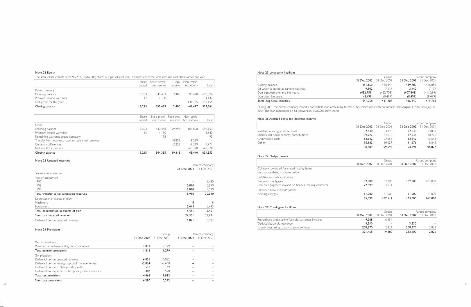
5150
Note 22 Equity
The share capital consists of 19,215,283 (19,202,583) shares of a par value of SEK1.All shares are of the same class and each share carries one vote.
Share Share premi- Legal Non-restric-capital um reserve reserve ted equity Total
Parent companyOpening balance 19,203 549,493 2,400 99,478 670,574Premium issued warrants 12 1,130 1,142Net profit for the year -148,155 -148,155
Closing balance 19,215 550,623 2,400 -48,677 523,561
Share Share premi- Restricted Non-restric-capital um reserve reserves ted reserves Total
GroupOpening balance 19,203 543,348 29,794 104,808 697,153Premium issued warrants 12 1,130 1,142Remaining warrants group company -93 -93Transfer from non-restricted to restricted reserves -8,229 8,229 –Currency differences -2,252 -1,219 -3,471Net result for the year -63,378 -63,378
Closing balance 19,215 544,385 19,313 48,440 631,353
Note 23 Untaxed reserves
Parent company31 Dec 2002 31 Dec 2001
Tax allocation reserves
Year of assessment1997 – 11,4301998 10,890 10,8901999 8,020 8,020
Total transfer to tax allocation reserves 18,910 30,340
Depreciation in excess of planMachinery 8 8Equipment 5,443 5,443
Total depreciation in excess of plan 5,451 5,451
Sum total untaxed reserves 24,361 35,791
Deferred tax on untaxed reserves 6,821 10,022
Note 24 Provisions
Group Parent company31 Dec 2002 31 Dec 2001 31 Dec 2002 31 Dec 2001
Pension provisionsPension commitments at group companies 1,812 1,279 – –
Total pension provisions 1,812 1,279 – –
Tax provisionsDeferred tax on untaxed reserves 6,821 10,022 – –Deferred tax on intra-group profit in inventories -2,824 -1,698 – –Deferred tax on exchange rate profits -16 169 – –Deferred tax expense on temporary differencies, etc. 487 520 – –
Total tax provisions 4,468 9,013 – –
Sum total provisions 6,280 10,292 – –
Note 25 Long-term liabilities
Group Parent company31 Dec 2002 31 Dec 2001 31 Dec 2002 31 Dec 2001
Closing balance 451,160 438,344 419,780 426,855Of which is stated as current liabilities -9,902 -7,137 -3,440 -7,137Due between one and five years (432,759) (422,708) (407,841) (411,219)Due after five years (8,499) (8,499) (8,499) (8,499)
Total long-term liabilities 441,258 431,207 416,340 419,718
During 2001 the parent company issued a convertible loan amounting to MSEK 320, which runs with no interest from August 1, 2001 until July 31,2004.The loan represents on full conversion 1,000,000 new shares.
Note 26 Accrued costs and deferred income
Group Parent company31 Dec 2002 31 Dec 2001 31 Dec 2002 31 Dec 2001
Installation and guarantee costs 32,638 33,898 32,638 33,898Salaries incl. social security contributions 39,927 32,610 37,535 30,776Commission costs 12,942 22,558 12,942 22,558Other 15,182 10,627 11,676 8,845
100,689 99,693 94,791 96,077
Note 27 Pledged assets
Group Parent company31 Dec 2002 31 Dec 2001 31 Dec 2002 31 Dec 2001
Collateral provided for stated liability itemson balance sheet is shown below:
Liabilities to credit institutionsProperty mortgages 102,000 102,000 102,000 102,000Lien on equipment owned on financial leasing contracts 22,599 4,511 – –
Unutilised bank overdraft facilityFloating charges 61,000 61,000 61,000 61,000
185,599 167,511 163,000 163,000
Note 28 Contingent liabilities
Group Parent company31 Dec 2002 31 Dec 2001 31 Dec 2002 31 Dec 2001
Repurchase undertaking for sold customer invoices 9,268 6,454 – –Deductible, credit insurance 3,530 – 3,530 –Future unertaking to pay to joint ventures 208,670 2,826 208,670 2,826
221,468 9,280 212,200 2,826
To the general meeting of the share-holders of Micronic Laser Systems ab(publ.) Corporate identity number556351-2374.
We have audited the annualaccounts, the consolidated accounts,the accounting records and the admin-istration of the Board of Directors andthe Managing Director of MicronicLaser Systems ab (publ.) for the year2002. These accounts and the admin-istration of the company are the respon-sibility of the Board of Directors andthe Managing Director. Our responsi-bility is to express an opinion on the annual accounts, the consolidatedaccounts and the administration basedon our audit.
We conducted our audit in accor-dance with generally accepted audit-ing standards in Sweden. Those stan-dards require that we plan and per-form the audit to obtain reasonableassurance that the annual accountsand the consolidated accounts are freeof material misstatement.
An audit includes examining, on a testbasis, evidence supporting the amountsand disclosures in the accounts. Anaudit also includes assessing theaccounting principles used and theirapplication by the Board of Directorsand the Managing Director, as well asevaluating the overall presentation ofinformation in the annual accountsand the consolidated accounts. As abasis for our opinion concerning dis-charge from liability, we examinedsignificant decisions, actions takenand circumstances of the company inorder to be able to determine the lia-bility, if any, to the company of anyboard member or the ManagingDirector. We also examined whetherany board member or the ManagingDirector has, in any other way, acted in contravention of the CompaniesAct, the Annual Accounts Act or theArticles of Association. We believethat our audit provides a reasonablebasis for our opinion set out below.
The annual accounts and the consoli-dated accounts have been prepared inaccordance with the Annual AccountsAct and, thereby, give a true and fairview of the company’s and the group’sfinancial position and results of oper-ations in accordance with generallyaccepted accounting principles inSweden.
We recommend to the generalmeeting of shareholders that theincome statements and balance sheetsof the parent company and the groupbe adopted, that the loss for the parentcompany be dealt with in accordancewith the proposal in the administra-tion report and that the members ofthe Board of Directors and theManaging Director be dischargedfrom liability for the financial year.
Auditors’ report
52 53
Executive management
Sven LöfquistBorn 1956. President and ceo. Employed since 1985. Master’sdegree in Electronic Engineering. Shareholding in Micronic (familyincluded): 132,500. Holding of warrants: 4,400.
Charlott SamuelssonBorn 1963. Vice President, System&ApplicationDevelopment. Employed since 1996. Master’s de-gree in Engineering Electrophysics. Shareholdingin Micronic: 3,000. Holding of warrants: 4,000.
Ulf SundströmBorn 1958. Sr. Vice President, Customer Operation.Employed since 1996. Master’s degree in EngineeringPhysics. Shareholding in Micronic: 13,333. Hold-ing of warrants: 4,400.
Jorge FreyerBorn 1950. Sr. Vice President, Marketing andBusiness Development. Employed since 1999.Master’s degree in Engineering. Shareholding inMicronic: 25,000. Holding of warrants: 3,000.
Per FridolinAuthorized public accountantLindebergs Grant Thornton AB
Stockholm, Sweden February 11, 2003.
Anders ÖstbergAuthorized public accountantLindebergs Grant Thornton AB
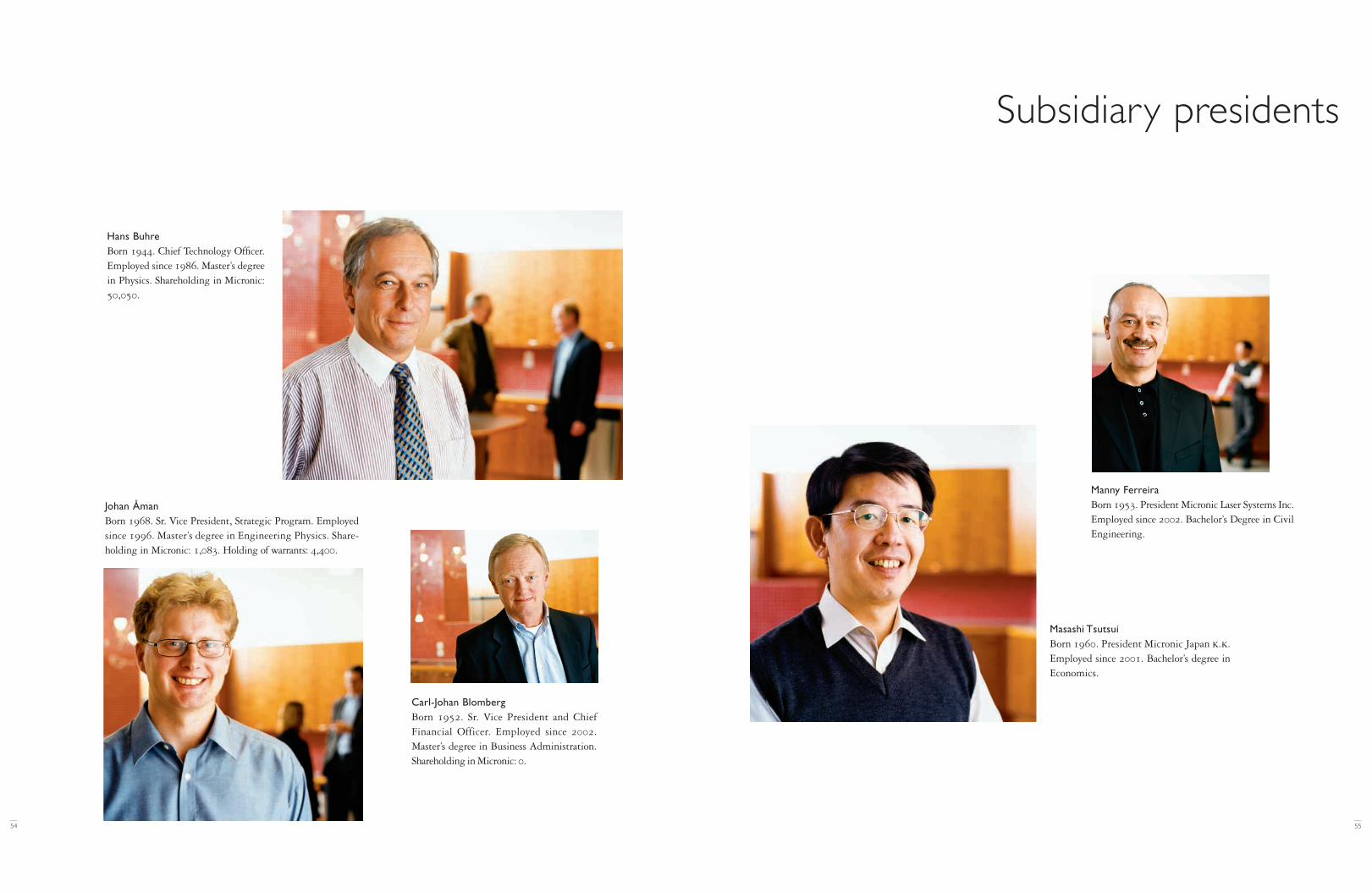
5554
Subsidiary presidents
Hans BuhreBorn 1944. Chief Technology Officer.Employed since 1986. Master’s degreein Physics. Shareholding in Micronic:50,050.
Manny FerreiraBorn 1953. President Micronic Laser Systems Inc.Employed since 2002. Bachelor’s Degree in CivilEngineering.
Masashi TsutsuiBorn 1960. President Micronic Japan k.k.Employed since 2001. Bachelor’s degree inEconomics.
Johan ÅmanBorn 1968. Sr. Vice President, Strategic Program. Employedsince 1996. Master’s degree in Engineering Physics. Share-holding in Micronic: 1,083. Holding of warrants: 4,400.
Carl-Johan BlombergBorn 1952. Sr. Vice President and ChiefFinancial Officer. Employed since 2002.Master’s degree in Business Administration.Shareholding in Micronic: 0.
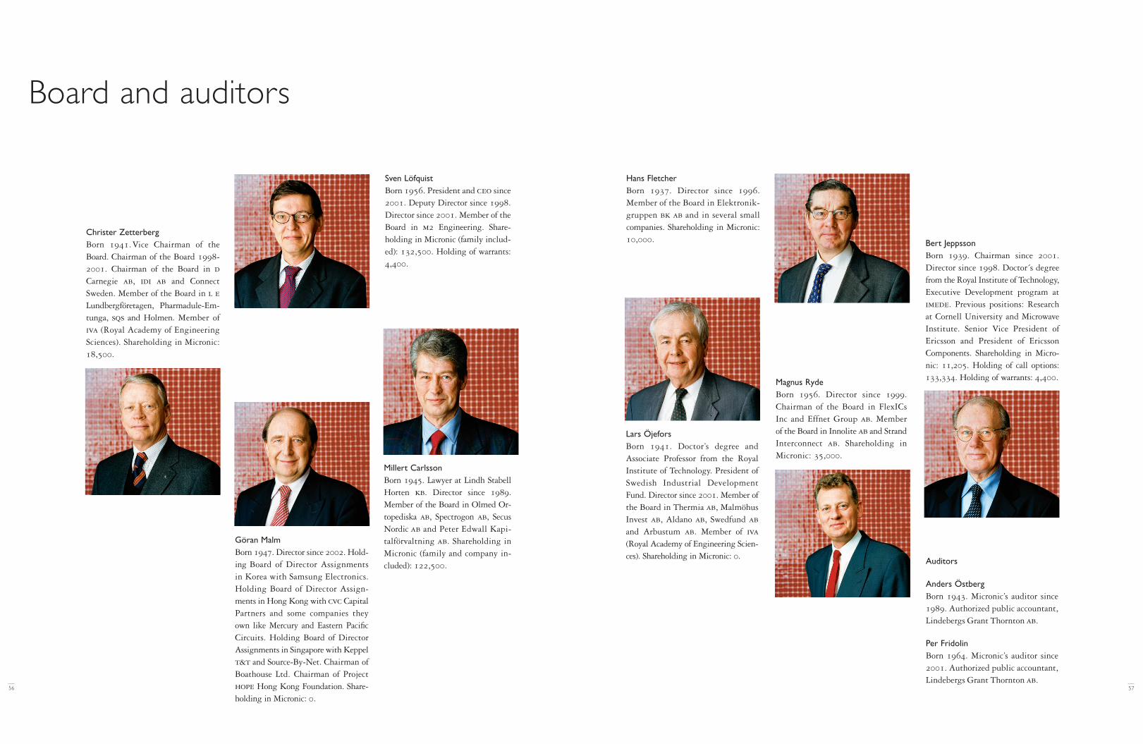
57
Board and auditors
56
Auditors
Anders ÖstbergBorn 1943. Micronic’s auditor since1989. Authorized public accountant,Lindebergs Grant Thornton ab.
Per FridolinBorn 1964. Micronic’s auditor since2001. Authorized public accountant,Lindebergs Grant Thornton ab.
Lars ÖjeforsBorn 1941. Doctor’s degree andAssociate Professor from the RoyalInstitute of Technology. President ofSwedish Industrial DevelopmentFund. Director since 2001. Member ofthe Board in Thermia ab, MalmöhusInvest ab, Aldano ab, Swedfund aband Arbustum ab. Member of iva(Royal Academy of Engineering Scien-ces). Shareholding in Micronic: 0.
Bert JeppssonBorn 1939. Chairman since 2001.Director since 1998. Doctor´s degreefrom the Royal Institute of Technology,Executive Development program atimede. Previous positions: Researchat Cornell University and MicrowaveInstitute. Senior Vice President ofEricsson and President of EricssonComponents. Shareholding in Micro-nic: 11,205. Holding of call options:133,334. Holding of warrants: 4,400.
Hans FletcherBorn 1937. Director since 1996.Member of the Board in Elektronik-gruppen bk ab and in several smallcompanies. Shareholding in Micronic:10,000.
Magnus RydeBorn 1956. Director since 1999.Chairman of the Board in FlexICsInc and Effnet Group ab. Memberof the Board in Innolite ab and StrandInterconnect ab. Shareholding inMicronic: 35,000.
Christer ZetterbergBorn 1941.Vice Chairman of theBoard. Chairman of the Board 1998-2001. Chairman of the Board in dCarnegie ab, idi ab and ConnectSweden. Member of the Board in l eLundbergföretagen, Pharmadule-Em-tunga, sqs and Holmen. Member ofiva (Royal Academy of EngineeringSciences). Shareholding in Micronic:18,500.
Millert CarlssonBorn 1945. Lawyer at Lindh StabellHorten kb. Director since 1989.Member of the Board in Olmed Or-topediska ab, Spectrogon ab, SecusNordic ab and Peter Edwall Kapi-talförvaltning ab. Shareholding inMicronic (family and company in-cluded): 122,500.
Sven LöfquistBorn 1956. President and ceo since2001. Deputy Director since 1998.Director since 2001. Member of theBoard in m2 Engineering. Share-holding in Micronic (family includ-ed): 132,500. Holding of warrants:4,400.
Göran MalmBorn 1947. Director since 2002. Hold-ing Board of Director Assignmentsin Korea with Samsung Electronics.Holding Board of Director Assign-ments in Hong Kong with cvc CapitalPartners and some companies theyown like Mercury and Eastern PacificCircuits. Holding Board of DirectorAssignments in Singapore with Keppelt&t and Source-By-Net. Chairman ofBoathouse Ltd. Chairman of Projecthope Hong Kong Foundation. Share-holding in Micronic: 0.
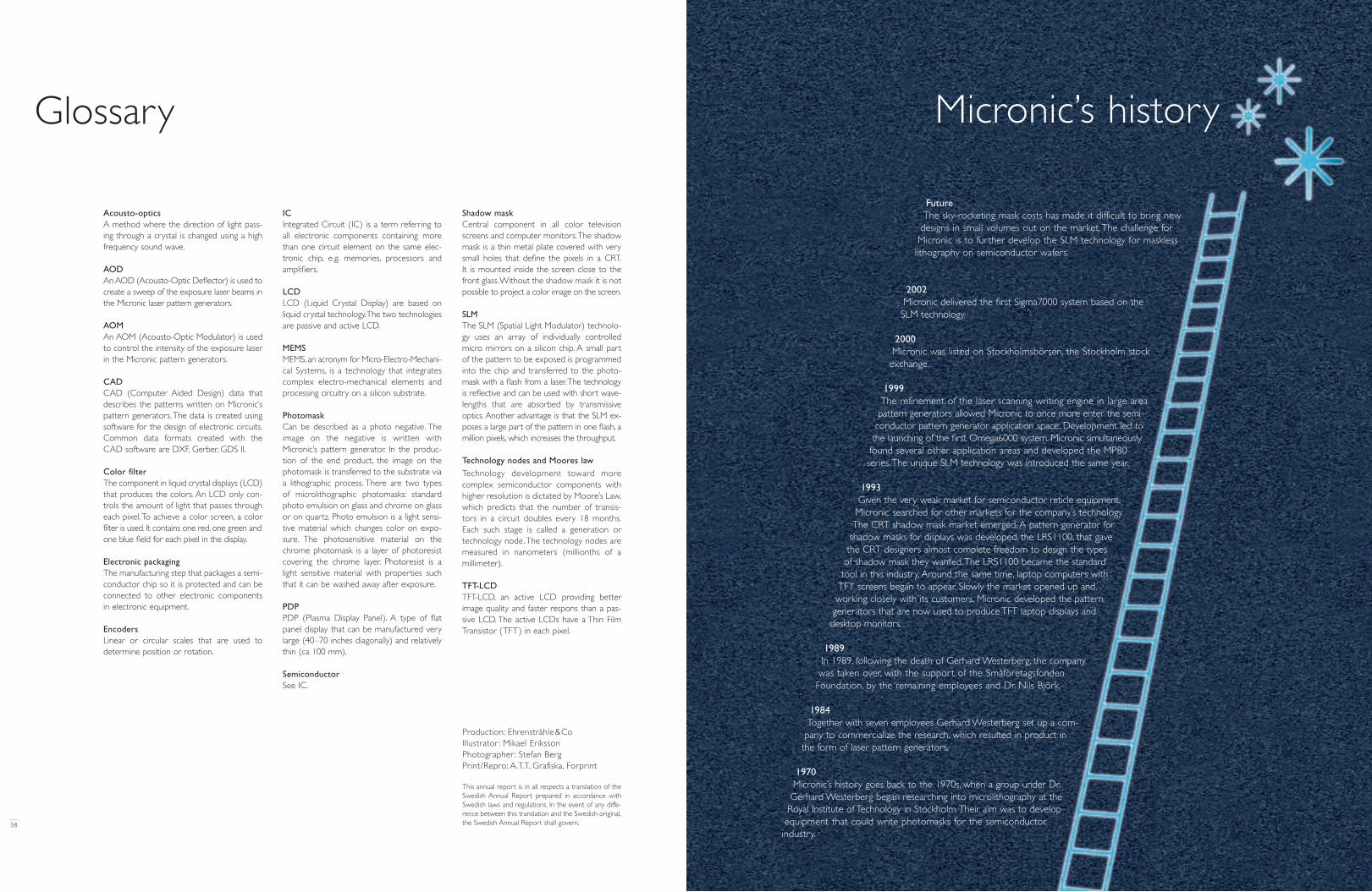
Acousto-optics A method where the direction of light pass-ing through a crystal is changed using a highfrequency sound wave.
AODAn AOD (Acousto-Optic Deflector) is used tocreate a sweep of the exposure laser beams inthe Micronic laser pattern generators.
AOM An AOM (Acousto-Optic Modulator) is usedto control the intensity of the exposure laserin the Micronic pattern generators.
CADCAD (Computer Aided Design) data thatdescribes the patterns written on Micronic’spattern generators.The data is created usingsoftware for the design of electronic circuits.Common data formats created with theCAD software are DXF, Gerber, GDS II.
Color filter The component in liquid crystal displays (LCD)that produces the colors. An LCD only con-trols the amount of light that passes througheach pixel.To achieve a color screen, a colorfilter is used. It contains one red, one green andone blue field for each pixel in the display.
Electronic packaging The manufacturing step that packages a semi-conductor chip so it is protected and can beconnected to other electronic componentsin electronic equipment.
Encoders Linear or circular scales that are used todetermine position or rotation.
ICIntegrated Circuit (IC) is a term referring toall electronic components containing morethan one circuit element on the same elec-tronic chip, e.g. memories, processors andamplifiers.
LCDLCD (Liquid Crystal Display) are based on liquid crystal technology.The two technologiesare passive and active LCD.
MEMSMEMS, an acronym for Micro-Electro-Mechani-cal Systems, is a technology that integratescomplex electro-mechanical elements andprocessing circuitry on a silicon substrate.
PhotomaskCan be described as a photo negative. Theimage on the negative is written withMicronic’s pattern generator. In the produc-tion of the end product, the image on thephotomask is transferred to the substrate viaa lithographic process. There are two types of microlithographic photomasks: standardphoto emulsion on glass and chrome on glassor on quartz. Photo emulsion is a light sensi-tive material which changes color on expo-sure. The photosensitive material on thechrome photomask is a layer of photoresistcovering the chrome layer. Photoresist is alight sensitive material with properties suchthat it can be washed away after exposure.
PDPPDP (Plasma Display Panel). A type of flatpanel display that can be manufactured verylarge (40–70 inches diagonally) and relativelythin (ca 100 mm).
SemiconductorSee IC.
Shadow maskCentral component in all color televisionscreens and computer monitors.The shadowmask is a thin metal plate covered with verysmall holes that define the pixels in a CRT.It is mounted inside the screen close to thefront glass.Without the shadow mask it is notpossible to project a color image on the screen.
SLMThe SLM (Spatial Light Modulator) technolo-gy uses an array of individually controlledmicro mirrors on a silicon chip. A small partof the pattern to be exposed is programmedinto the chip and transferred to the photo-mask with a flash from a laser.The technologyis reflective and can be used with short wave-lengths that are absorbed by transmissiveoptics. Another advantage is that the SLM ex-poses a large part of the pattern in one flash, amillion pixels, which increases the throughput.
Technology nodes and Moores law
Technology development toward morecomplex semiconductor components withhigher resolution is dictated by Moore’s Law,which predicts that the number of transis-tors in a circuit doubles every 18 months.Each such stage is called a generation ortechnology node.The technology nodes aremeasured in nanometers (millionths of amillimeter).
TFT-LCDTFT-LCD, an active LCD providing betterimage quality and faster respons than a pas-sive LCD. The active LCDs have a Thin FilmTransistor (TFT) in each pixel.
Glossary
58
This annual report is in all respects a translation of theSwedish Annual Report prepared in accordance withSwedish laws and regulations. In the event of any diffe-rence between this translation and the Swedish original,the Swedish Annual Report shall govern.
Production: Ehrenstråhle&Co Illustrator : Mikael ErikssonPhotographer : Stefan BergPrint/Repro: A.T.T. Grafiska, Forprint
FutureThe sky-rocketing mask costs has made it difficult to bring new
designs in small volumes out on the market.The challenge forMicronic is to further develop the SLM technology for maskless
lithography on semiconductor wafers.
2002Micronic delivered the first Sigma7000 system based on the
SLM technology.
2000Micronic was listed on Stockholmsbörsen, the Stockholm stock
exchange.
1999The refinement of the laser scanning writing engine in large area
pattern generators allowed Micronic to once more enter the semi-conductor pattern generator application space. Development led to
the launching of the first Omega6000 system. Micronic simultaneouslyfound several other application areas and developed the MP80
series.The unique SLM technology was introduced the same year.
1993Given the very weak market for semiconductor reticle equipment,
Micronic searched for other markets for the company’s technology.The CRT shadow mask market emerged. A pattern generator for
shadow masks for displays was developed, the LRS1100, that gavethe CRT designers almost complete freedom to design the types
of shadow mask they wanted.The LRS1100 became the standardtool in this industry. Around the same time, laptop computers with
TFT screens began to appear. Slowly the market opened up and,working closely with its customers, Micronic developed the pattern
generators that are now used to produce TFT laptop displays anddesktop monitors.
1989In 1989, following the death of Gerhard Westerberg, the company
was taken over, with the support of the SmåföretagsfondenFoundation, by the remaining employees and Dr. Nils Björk.
1984Together with seven employees Gerhard Westerberg set up a com-
pany to commercialize the research, which resulted in product in the form of laser pattern generators.
1970Micronic’s history goes back to the 1970s, when a group under Dr.
Gerhard Westerberg began researching into microlithography at theRoyal Institute of Technology in Stockholm.Their aim was to develop
equipment that could write photomasks for the semiconductorindustry.
Micronic’s history
Micronic Laser Systems AB (publ.)Nytorpsvägen 9Box 3141, 183 03 Täby, SwedenTel: +46 8 638 52 00Fax: +46 8 638 52 90E-mail: [email protected]
Micronic Strategic DevelopmentMölndalsvägen 91412 63 Göteborg, SwedenTel: +46 31 703 06 80Fax: +46 31 703 06 90
Micronic Laser Systems Inc.2922 Scott BoulevardSanta Clara, CA 95054, USATel: +1 408 235 7720Fax: +1 408 855 9846
Micronic Japan K.K.Masumoto Building 3F7-4-3, Nishishinjuku, Shinjuku-kuTokyo 160-0023, JapanTel: +81 3 3227 8218Fax: +81 3 3227 8217
Micronic Laser Systems Far East Co., Ltd.9th Floor, #18 Pu-Ding RoadDer-An BuildingHsinchu 300,TaiwanTel: +886 3 564 6656Fax: +886 3 564 6664
Micronic Laser Systems AB Shanghai Representative OfficeRoom J, Floor 24,International Shipping & Finance Center720 Pudong Dadao200120 Shanghai, ChinaTel: +86 21 503 68383Fax: +86 21 503 68181
Pushing the limits


