Journal of Engineering and Development, Vol. 10, No. 2, June (2006) ISSN 1813-7822 72 Parametric Study of the Rectangular Microstrip Antenna using Cavity Model Abstract A cavity model well suited for computer aided design is presented and developed to study the rectangular microstrip antenna. The patch is described by geometrical and electrical parameters. The resonant frequency, resonant resistance, bandwidth, efficiency and other electrical parameters of RMSA have been presented as a function of varying the patch dimension and substrate parameters. The accuracy and usefulness of the method are investigated through comparison with experimental results as well as other previous theoretical methods. الخ ـص ـــــــ ة تم استخدام إمستطيلة حيثيقة الت الشريطية الدقئيامي لدراسة الهوا بناء وتطوير برنامج تصميجوة فيوب الف سلحديد معلمات تم ت وأبعادفعال المستطيل ال( patch ) ومة الرنينيةلمقاني وا التردد الرني حساب كل منندسيا وكهربائيا وتم هءة الهوائيلحزمة وكفا وعرض اضافة با إلىمعلمات الخرى استها مع تغيير والتي تم درا أبعادفعال وبينت المستطيل السات منشورة.ت النظرية لدرالحسابا التجريبية والحالي مقارنة بالنتائجمج البرنا ا يعطيهاة التيلعاليئج الدقة النتا اProf. Dr. Jamal W. Salman Electrical Eng. Dept., College of Engineering Al-Mustansiriya University, Baghdad, Iraq Asst. Prof. Dr. Mudhaffer M. Ameen Electrical Eng. Dept., College of Engineering Salahaddin University, Salahaddin, Iraq Lect. Star O. Hassan Electrical Eng. Dept., College of Engineering Salahaddin University, Salahaddin, Iraq
Transcript
Journal of Engineering and Development, Vol. 10, No. 2, June (2006) ISSN 1813-7822
72
Parametric Study of the Rectangular Microstrip Antenna using Cavity Model
Abstract
A cavity model well suited for computer aided design is presented and developed to
study the rectangular microstrip antenna. The patch is described by geometrical and
electrical parameters. The resonant frequency, resonant resistance, bandwidth, efficiency
and other electrical parameters of RMSA have been presented as a function of varying
the patch dimension and substrate parameters. The accuracy and usefulness of the
method are investigated through comparison with experimental results as well as other
previous theoretical methods.
ةـــــــالصـالخ
سلوب الفجوة في بناء وتطوير برنامج تصميمي لدراسة الهوائيات الشريطية الدقيقة المستطيلة حيث إتم استخدام هندسيا وكهربائيا وتم حساب كل من التردد الرنيني والمقاومة الرنينية (patch)المستطيل الفعال وأبعادتم تحديد معلمات
المستطيل الفعال وبينت أبعادوالتي تم دراستها مع تغيير األخرىالمعلمات إلى باإلضافة وعرض الحزمة وكفاءة الهوائي النتائج الدقة العالية التي يعطيها البرنامج الحالي مقارنة بالنتائج التجريبية والحسابات النظرية لدراسات منشورة.
Prof. Dr. Jamal W. Salman
Electrical Eng. Dept., College of Engineering
Al-Mustansiriya University, Baghdad, Iraq
Asst. Prof. Dr. Mudhaffer M. Ameen
Electrical Eng. Dept., College of Engineering
Salahaddin University, Salahaddin, Iraq
Lect. Star O. Hassan
Electrical Eng. Dept., College of Engineering
Salahaddin University, Salahaddin, Iraq
Journal of Engineering and Development, Vol. 10, No. 2, June (2006) ISSN 1813-7822
73
1. Introduction
Modern communication systems demand low coast and low profile antennas.
Microstrip antenna (MSA) is one of the candidate antennas meeting those requirements due
to its conformal nature and capability to integrate with the rest of the printed circuitry [1]
.
The MSA is a resonant structure that consists of a dielectric substrate sandwiched
between a metallic conducting patch and a ground plane. The patch is generally made of
copper or gold and can take any possible shape [2,3]
.
During the past decades, microstrip antennas experienced a great gain in popularity and
hence become a major research topic in both theoretical and applied electromagnetic. They
are well known for their highly desirable physical advantage characteristics [4]
.However, two
principal disadvantages of MSA are narrow bandwidth and low gain. Numerous researches
have investigated their basic characteristics and recently extensive efforts have also been
devoted to the bandwidth and gain problems and considerable progress have been made [5-10]
.
There is a number of techniques available for analyzing microstrip patch antennas. The
analytical techniques include transmission line model [11-13]
, and cavity model [14-16]
. The
most common numerical techniques used are moment method [17]
and the finite difference
time domain method [18]
. The later technique is time consuming while the former method and
the analytical techniques have been applied to regular shapes only like, rectangular, circular,
and elliptical shapes [11]
. However, the analysis of MSA is normally difficult to handle which
is primarily due to the existence of a dielectric substrate to support the conductor [19]
.
The aim of this work is to use the cavity model to study the rectangular microstrip
antennas operating in the range of (3GHz) which excited by a coaxial feed. For this purpose a
computer program written in Fortran-77 language, which is based on the cavity model is
presented and developed for the first time prior to this work. Moreover, this program has
been also modified in order to investigate the effect of various parameters on the
performance of rectangular microstrip antennas operating in the range of (3GHz).
2. Theory
2-1 Resonance Frequency and RMSA Dimension
The MSA consists a conducting plate separated from a ground plane usually by a thin
layer of dielectric. A shape of rectangular microstrip antenna is shown in Fig.(1). A cavity
model was used to calculate the resonant frequencies whenever a magnetic wall is introduced
at the sides of the patch while the electric wall is introduced at the bottom and top of the
patch. By employing this simple model, the dominant TM10-resonant frequency mode of
RMSA is given by [14]
:
effeff
r.L.2
cf
……………………………………………………………...... (1)
Journal of Engineering and Development, Vol. 10, No. 2, June (2006) ISSN 1813-7822
74
where, (c) is the velocity of electromagnetic waves in space, Leff and εeff are effective length
and effective dielectric substrate permittivity respectively. The effective length is given
by [20]
:
LLLeff …………………………………………………………………... (2)
Since the length of the patch has been extended by (ΔL) on each side so it can be
expressed by [21]
:
)8.0h
W).(258.0(
)264.0h
W).(3.0(
.h.412.0L
eff
eff
……………………………………….. (3)
where, (h) is the substrate thickness and (W) is the width of the patch which is given by [20]
:
1
2
f.2
cW
rr ……………………………………………………………… (4)
While the effective dielectric substrate permittivity can be expressed as [22]
:
W
h.121.2
1
2
1 rreff
……………………………………………………. (5)
Figure (1) Microstrip antenna element
W L
Z
X
Y
Ground conductor
Microstrip patch
Journal of Engineering and Development, Vol. 10, No. 2, June (2006) ISSN 1813-7822
75
2-2 Radiation Pattern of Rectangular Patch
The far-field radiation pattern of a rectangular microstrip patch operating in the
TM10-mode is broad in the E and H-planes. The pattern of a cavity with two perfectly
conducting electric walls (top and bottom), and four perfectly conducting magnetic walls
(side walls) are given by [20]
:
0E
0Er………………………………………………………………………. (6-a)
)Sin.sin.2
L.k(Cos].
Z
SinZ.
X
SinX.Sin.[.
r.
V.W.k.jE effor.k.joo
eo
…………... (6-b)
where,
Cos.2
W.kZ
Cos.Sin.2
h.kX
o
o
…………………………………………………………. (7)
and Vo=h.Eo is the voltage across sides of radiating edge of the patch, then, the principal E
and H-planes reduces to:
E-plane (θ=90, 0≤Ф≤ 90, and 270≤Ф≤360):
)Sin.2
L.kCos].
Cos.2
h.k
)Cos.2
h.k(Sin
.[.r.
V.W.k.jE effo
o
o
r.k.joo
eo
……... (8)
and H-Plane (Ф=0 , 0≤θ≤180):
]
Cos.2
W.k
)Cos.2
W.k(Sin
*
Sin.2
h.k
)Sin.2
h.k(Sin
.Sin.[.r.
V.W.k.jE
o
o
o
o
r.k.joo
eo
……. (9)
2-3 Input Impedance
The input impedance of a RMSA excited by a coaxial feed can be determined by
returning to the cavity model approximation for the fields in the patch. The input impedance
is given by Ohms law:
oI
VinZin ……………………………………………………………………. (10)
Journal of Engineering and Development, Vol. 10, No. 2, June (2006) ISSN 1813-7822
76
With Vin is the input voltage at the feed-point and it can be computed as [23]
:
mn2
mn
2
ffmn2
o0 G.kk
)y,x.(I.h..w.jVin
……………………………………….. (11)
where,
)W
x..n(Cos).
L
y..m(Cos.
W.L
. ffnmmn
………………………………….. (12-a)
0p.for.
0p.for
2
1p
…………………………………………………………. (12-b)
L.2
d..n
)L.2
d..n(Sin
.
W.2
d..m
)W.2
d..m(Sin
Gy
y
x
x
mn
…………………………………………... (13)
and,
).j1.(.kk effr
2
o
2 ………………………………………………………. (14)
Equation (10), can then be evaluated for the dominant TM10-mode at k2=k10
2.εr which
leaves the input resistance as [24]
:
)L
x.(Cos.
.W.L..k
h.f..4Rin f2
effro2
o.r
………………………………………….. (15)
where, (xf) is a distance from the edge of the patch and (δeff=1/Qt), where Qt can be
calculated using section 2-5. However, there is another accurate expression for the input
resistance of RMSA excited by a coaxial feed given by [25]
as:
)L
x.(Sin.RRin f2
e
…………………………………………………………. (16)
where, (xf) is a distance from the center of the patch, and
)GG.(2
1R
mr
e
…………………………………………………………… (17)
where, (Gr)is the radiation conductance which is given in section 2-4, and Gm is the mutual
conductance and it is expressed as [25]
:
Journal of Engineering and Development, Vol. 10, No. 2, June (2006) ISSN 1813-7822
77
grm F.GG ………………………………………………………………….. (18)
)l(J.p24
p)l(JF 22
2
0g
……………………………………………………. (19)
where, )LL(kl , Lkp , )l(J and )l(J2 are zero and second order Bessel functions,
respectively.
2-4 Power and Directivity
The radiation power (Prad) over a sphere of radius (r) is given by a definition of the
Pointing vector as [20]
:
d.d.Sin.r).HE(..2
1P
2*
rad
………………………………………. (20)
where, is the characteristic impedance of space and equal to (120π)Ω ,Then, for a RMSA
operating in the dominant TM10-mode, Eq.(20), becomes:
d.d.Sin.)]Cos.Sin.2
L.k(Cos.[]
Z
SinZ.
X
SinX.Sin[.
.240
)k.W.(VP
2effo2
3
2
o
2
o
rad …... (21)
So the radiation conductance (Gr) is given by:
2
0
radr
V
P.2G …………………………………………………………………... (22)
The usual HPBW is defined by the angles at which the antenna element power pattern
falls 3dB below the main beam peak [26]
and the relation of E-and H-plane of HPBW are
given by [23]
:
2
o
22
1
Ek).hL.3(
03.7Sin.2
………………………………………………… (23)
W.k2
1Sin.2
o
1
H
……………………………………………………... (24)
The directivity of an antenna is defined as the ratio of the radiation intensity in a given
direction from the antenna to the radiation intensity averaged over all directions, and
mathematically can be expressed as:
Journal of Engineering and Development, Vol. 10, No. 2, June (2006) ISSN 1813-7822
78
rad
maxr
P
U..4D
……………………………………………………………….. (25)
For RMSA-operating at TM10-mode, the directivity is given by:
rad
2
2
or
G..30
)K.W(D
……………………………………………………………... (26)
2-5 Quality Factors, Bandwidth, Efficiency and Gain
At resonance, the MSA element can be assigned a quality factor, Qt, to describe its
bandwidth. The Qt factor is the total of all quality factors associated with system losses,
which include dissipated losses within the patch due to loss metal conductors and substrates,
power loss due to radiation and surface wave propagation on a dielectric coated conductor.
For very thin substrate (h<<λo) of arbitrary shapes (including rectangular and circular) there
are approximate formulas to represent the quality factors of various losses [20-21]
. These can
be expressed as:
rad
rrrad
d
roc
G.h
L.W..f.Q
tan
1Q
f....hQ
………………………………………………………… (27)
where, (μo is a permeability =4π*10-9
H/cm, ζ is the copper conductivity =5.7*105 S/cm, fr is
the resonance frequency in Hz and tanδ is the loss tangent). Therefore, the total quality factor
Qt influenced by all of these losses and is, in general, written as [21]
:
dcradt Q
1
Q
1
Q
1
Q
1 ……………………………………………………….. (28)
The fractional bandwidth of MSA elements is usually determined from the total quality
factors with (VSWR=2:1) and is given by:
s.Q
1sBW
t
………………………………………………………………… (29)
The radiation efficiency is defined as the ratio of the power radiated to the power
received by the input to the element. It can also be expressed in terms of the quality factors,
which for a MSA, can be written as [20]
:
Journal of Engineering and Development, Vol. 10, No. 2, June (2006) ISSN 1813-7822
79
t
rad
Q
Q ……………………………………………………………………… (30)
However, the antenna gain is a measure of an antennas ability to concentrate the power
accepted at input terminal and mathematically is related to the directivity and efficiency as:
rD.Gain ………………………………………………………………….. (31)
All the above equations have been formulated in the computer program in several
subroutines to identify their values with respect to the variation of various parameters of
RMSA, excited by a coaxial feed.
3. Results and Discussion
To test the accuracy of the computer program, which is based on the cavity model, the
resonance frequency and resonance resistance of TM10-mode have been calculated.
Table (1), represents the results obtained in this work and compared with measured values of
Ref. [27]
and other previous theoretical methods [16,17]
,for different values of (εr, h, w, L, and
tanδ). It is obviously seen that the resonant frequencies obtained in this work are in good
agreement with measure data compared to the other theoretical methods. However, there are
some discrepancies between the measured and calculated resonant resistances. The reasons
can be explained these differences are attributed to the surface wave effect which is assumed
to be negligible in this work and the fields are assumed to be constant in the direction normal
to the substrate planes [27]
. Moreover, the computed resonant resistances, by using Eq.(16),
are better than those obtained with Eq.(15) in comparison with measured values. After that
the effect of varying various parameters of RMSA such as dielectric constant, width,
substrate thickness and loss tangent (tanδ) have been carried out using the computer program
which is based on the cavity model.
The dimension of the RMSA has been taken as: (W=4 cm, L=3 cm, h=0.159 cm,
εr=2.55 and tanδ=0.001).
3-1 The Effect of Varying the Dielectric Constant (r)
The effect of varying the dielectric constant (εr) from (1 to 2.6) on the electrical
properties of RMSA with the feed-point fixed at (0.7 cm) from the center of the patch are
shown in Fig.(2) for bandwidth and Fig.(3) for both directivity and antenna gain. It is clearly
seen that, the bandwidth decreases from (187.9 to 60 MHz), the gain decreases from (9.62 to
6.68 dB) and directivity decreases from (9.75 to 6.96 dB). So the dielectric constant of higher
value of permittivity gives lower electrical parameters of RMSA. However, when the
feed-point location is optimized for each (εr) and the dimensions of the RMSA are scaled to
operate at around (3 GHz) then a better comparison of the effect of (εr) can be obtained.
Table (2), represents the computed and measured values of some electrical properties of
Journal of Engineering and Development, Vol. 10, No. 2, June (2006) ISSN 1813-7822
80
RMSA for four different values of (εr).One can sees that our calculated results of bandwidth,
gain and resonance resistance are very close to their corresponding measured values. In
addition, as the (εr) increases from (1 to 9.8) the bandwidth decrease from (82.7 to 26.6
MHz) due to a decreases in the fringing fields. Also, the gain decrease from (9.6 to 4.7 dB)
due to a decrease in the aperture area.
Table (1) Comparison of calculated and measured values of resonant
frequency and resonant resistance of the rectangular patch with
different εr, tanδ, and substrate thickness
ε r
h (
cm)
Xf (c
m)
W (
cm)
L (
cm)
tan
δ
Resonance frequency
(GHz)
Resonance resistance
(Ω ) m
.v.
p.w
.
[17]
[16]
m.v
. P.W.
[17]
[16]
Eq.16 Eq.15
fr.
fr.
fr.
fr.
Rin
Rin
Rin
Rin
Rin
2.2
2
0.0
79
0.4
4
2.5
0.0
009
3.9
4
3.9
5
3.8
9
3.8
9
89
82
.67
10
2
10
1
83
2.2
2
0.0
79
0.2
2
1.2
5
0.0
009
7.6
5
7.7
4
7.6
1
7.5
3
99
84
.63
11
0
13
0
81
2.2
2
0.1
5
0.4
4
2.5
0.0
009
3.8
4
3.8
7
3.8
1
3.7
7
87
84
.47
11
0
12
7
81
2.5
0.1
524
2.0
7
4.1
4
4.1
4
0.0
01
2.2
3
2.2
6
2.2
7
----
-
28
4
25
9
31
6
39
7
----
--
2.5
0.1
524
2.0
7
6.8
58
4.1
4
0.0
01
2.2
0
2.2
4
2.2
3
----
-
10
8
10
6.8
13
5
18
0
----
--
2.5
0.1
524
2.0
7
10
.8
4.1
4
0.0
01
2.1
8
2.2
3
2.2
1
----
-
53
54
.17
69
.7
90
----
--
10
.2
0.1
27
0.6
5
3
2
0.0
023
2.2
6
2.3
2
2.2
8
2.2
3
85
90
.73
82
.3
10
0
72
10
.2
0.1
27
0.3
2
15
0.9
5
0.0
023
4.4
9
4.7
7
4.5
8
4.4
3
53
73
.91
81
.7
75
56
10
.2
0.2
54
0.6
5
3
1.9
0.0
023
2.2
4
2.3
8
2.2
9
2.2
1
80
69
.61
78
.2
75
53
m.v.= measured value
p.w.= present work
Journal of Engineering and Development, Vol. 10, No. 2, June (2006) ISSN 1813-7822
81
Figure (2) Variations of bandwidth versus the substrate permittivity (εr)
Figure (3) Variations of directivity and gain versus the substrate
permittivity (εr)
10
60
110
160
210
1 1.5 2 2.5 3
Ban
dw
idth
(M
Hz)
r
6
7
8
9
10
1 1.5 2 2.5 3
Directivity Gain
Dir
ec
tivit
y a
nd
Ga
in
εr
Journal of Engineering and Development, Vol. 10, No. 2, June (2006) ISSN 1813-7822
82
Table (2) Comparison of calculated and measured values of the effect of the substrate permittivity on the electrical properties of RMSA
with (h=0.159 cm and tanδ=0.001)
ε r
W (
cm)
L (
cm)
Xf (c
m)
Rin (Ω) Frequency
(GHz)
Bandwidth
(MHZ) Gain (dB)
m.v
. p.w.
m.v
.
p.w
.
m.v
.
p.w
.
m.v
.
p.w
.
Eq.16 Eq.15
1
6.2
4.6
5
1
54
48
.4
62
.7
2.9
9
3.0
7
74
82
.7
10
9.6
2.5
5
4.0
3.0
0.6
5
62
62.4
80
.1
2.9
7
3.0
5
64
61
.7
6.8
6.7
4.3
3.1
2.3
0.4
52
56
.63
70
.9
2.9
8
3.0
8
49
47
.2
5.6
5.7
9.8
2.0
1.5
1
0.2
51
66
.7
80
.7
3.0
2
3.1
2
30
26.6
4.4
4.7
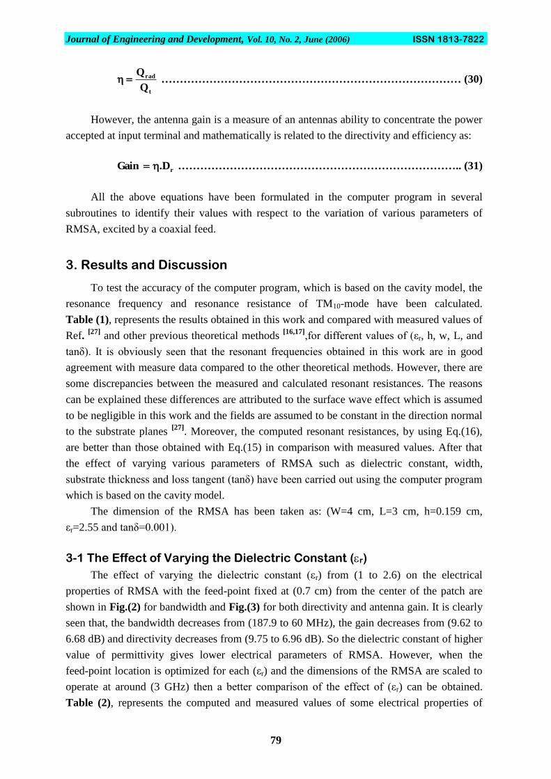
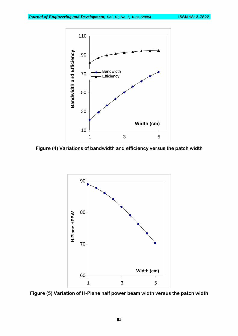
3-2 The Effect of Varying the Value of the Width (W)
The effect of varying the value of the width (W) from (1 to 5 cm) on the electrical
properties of RMSA with feeding point located (0.7 cm) from the edge is shown in Fig.(4)
for bandwidth and efficiency and Fig.(5) for H-plane HPBW. It is seen that the bandwidth
increases fro (21 to 71 MHz) and efficiency increased from (81.32 to 94.73 %), while the
H-plane HPBW decreases from (89 to 70). However, they are not very evident from these
plots, because the feed point is not optimum for the different width. Accordingly, a better
comparison will be obtained when the feed point is optimized for the individual widths.
Table (3) represent the measured and calculated resonant frequency, resonant resistance by
using Eq.(16), bandwidth, gain and H-plane HPBW with the computed value of directivity
and efficiency. This table indicates that computed results of electrical parameters of RMSA
are in good agreement with the corresponding measured values. Furthermore, except the
value of H-plane HPBW, all the other parameters are increased with increasing the value of
the width due to an increase in the aperture area of the patch. While the HPBW in the
H-plane decreases, whereas it remains almost the same in the E-plane, because the increase
in the width is in the H-plane.
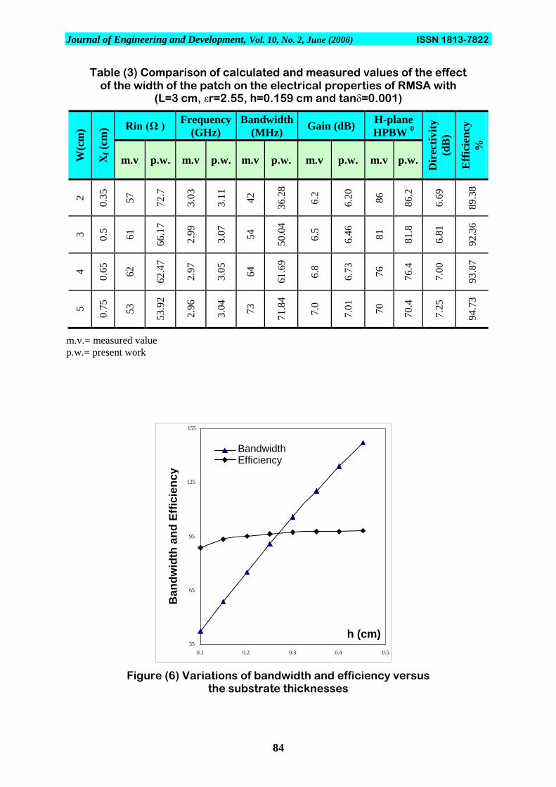
3-3 The Effect of Varying the Substrate Thicknesses (h)
The effect of varying the substrate thicknesses (h) on the bandwidth and efficiency of
RMSA with (εr=2.55, W=4 cm, L=3 cm, tanδ=0.001 and feed-point xf=0.7) are shown in
Fig.(6). It is observed that the bandwidth increases from (42.32 to 147.26 MHz) and
efficiency increased from (88.65 to 98.23 %) due to an increase in the radiation power. This
implies that, thicker substrate gives higher values of electrical parameters of RMSA.
Journal of Engineering and Development, Vol. 10, No. 2, June (2006) ISSN 1813-7822
83
Figure (4) Variations of bandwidth and efficiency versus the patch width
Figure (5) Variation of H-Plane half power beam width versus the patch width
10
30
50
70
90
110
1 3 5
Width (cm)
Ban
dw
idth
an
d E
ffic
ien
cy
Bandwidth Efficiency
60
70
80
90
1 3 5
Width (cm)
H-P
lan
e H
PB
W
Journal of Engineering and Development, Vol. 10, No. 2, June (2006) ISSN 1813-7822
84
Table (3) Comparison of calculated and measured values of the effect of the width of the patch on the electrical properties of RMSA with
(L=3 cm, εr=2.55, h=0.159 cm and tanδ=0.001)
W(c
m)
Xf (c
m) Rin (Ω )
Frequency
(GHz)
Bandwidth
(MHz) Gain (dB)
H-plane
HPBW 0
Dir
ecti
vit
y
(dB
)
Eff
icie
ncy
%
m.v p.w. m.v p.w. m.v p.w. m.v p.w. m.v p.w.
2
0.3
5
57
72
.7
3.0
3
3.1
1
42
36
.28
6.2
6.2
0
86
86
.2
6.6
9
89
.38
3
0.5
61
66
.17
2.9
9
3.0
7
54
50
.04
6.5
6.4
6
81
81
.8
6.8
1
92
.36
4
0.6
5
62
62
.47
2.9
7
3.0
5
64
61
.69
6.8
6.7
3
76
76
.4
7.0
0
93
.87
5
0.7
5
53
53.9
2
2.9
6
3.0
4
73
71.8
4
7.0
7.0
1
70
70.4
7.2
5
94.7
3
m.v.= measured value
p.w.= present work
Figure (6) Variations of bandwidth and efficiency versus the substrate thicknesses
35
65
95
125
155
0.1 0.2 0.3 0.4 0.5
Ban
dw
idth
an
d E
ffic
ien
cy
Bandwidth Efficiency
h (cm)
Journal of Engineering and Development, Vol. 10, No. 2, June (2006) ISSN 1813-7822
85
3-4 The Effect of Increasing the Value of Loss Tangent (tan)
Finally, the effect of increasing the value of loss tangent (tanδ) on the bandwidth and
efficiency of RMSA is investigated with (εr=2.55, h=0.159, W=4 cm, L=3 cm and feed-point
xf=0.7 cm from the center of the patch) and is shown in Fig.(7). It is seen that, with an
increase in the value of (tanδ) the bandwidth increases from (81.4 to 167.78 MHz) and
efficiency decreases from (71.45 to 34.66 %). So the use of loss material leads to increase the
bandwidth and to reduce the efficiency which gives lower gain.
Figure (7) Variations of bandwidth and efficiency of RMSA versus the loss tangent
4. Conclusion
As a result of the effect of varying the patch dimension and substrate properties on the
electrical properties of RMSA, we arrived to the following conclusion.
1. The computed results of resonance frequency and resonance resistance values obtained
with present method are in good agreement with the reported experimental and
theoretical values.
2. The advantage of the cavity model is that has faster speed of computation and
reasonably good accuracy. However, the disadvantages are that the antenna should be
symmetrical with respect to the feed-axis and the variation along the width should be
small.
3. In order to design a RMSA operating at high efficiency with broader bandwidth and
higher gain, its desirable to use a material with lower dielectric substrate permittivity,
and thicker substrate of higher losses. In addition the width of the patch must be as large
as possible for a given frequency to increase its radiation power.
0
30
60
90
120
150
180
0.01 0.02 0.03 0.04 0.05
Loss tangent Ban
dw
idth
an
d E
ffic
ien
cy
Bandwidth Efficiency
Journal of Engineering and Development, Vol. 10, No. 2, June (2006) ISSN 1813-7822
86
5. References
1. Ramesh, M., and Yip K., “Design Formula for the Inset Fed Patch Antenna”,
Journal of Microwave and Optoelectronics, Vol. 3, December 2003, pp.5-10.
2. Punit, S. Nakar, “Design of a Compact Microstrip Patch Antenna for use in
Wireless/Cellular Devices”, M.Sc. Thesis, University of Florida, College of
Engineering, Dept. of Electrical and Computer Engineering, 2004.
3. Andrew, T. Gobien, “Investigation of Low-Profile Antenna Designs for use in
Hand-Held Radios”, M.Sc. Thesis, Virginia Polytechnic Institute and State
University, 1997.
4. Esin, C., Stuart, A. Long, and William, F. Richards, “An Experimental of
Electrically Thick Rectangular Microstrip Antennas”, IEEE Trans. on Antenna
and Propagation, Vol. AP-43, No. 6, June 1986, pp.767-772.
5. Singhal, P. K., Bhawana, D., and Smita, B., “A Stacked Square Patch Slotted
Broadband Microstrip Antenna”, Journal of Microwave and Optoelectronics,
Vol. 3, No. 2, 2003, pp.60-66.
6. Debatosh, G., “Broadband Design of Microstrip Antennas: Recent Trends and
Developments”, Series, Mechanics, Automatic Control and Robotics, Vol. 3,
No. 15, April 2003, pp.1083-1088.
7. Zihfang, L., Panos, Y. Papalambros, and John, L. Volakis, “Designing Broadband
Patch Antennas using the Sequential Quadratic Programming Method”, IEEE
Trans. on Antenna and Propagation, Vol. 45, No. 11, November 1997,
pp.1689-1692.
8. Keith, C. Huie, “Microstrip Antennas: Broadband Radiation Patterns using
Photonic Crystal Substrates”, M.Sc. Thesis, Virginia Polytechnic Institute and
State University, 2002.
9. Tayeb, A. Denini, and Larbi, T., “High Gain Microstrip Antenna Design for
Broadband Wireless Applications”, Journal of Radio Frequency and Microwave
CAE, Vol. 13, June2003, pp.511-517.
10. Sersf, S., Kerim, G., and Mehmet, E., “Calculation of Bandwidth for Electrically
Thin and Thick Rectangular Microstrip Antennas With the use of Multilayered
Perceptions”, Journal of Radio Frequency and Microwave CAE, Vol. 9, 1991
pp.277-286.
Journal of Engineering and Development, Vol. 10, No. 2, June (2006) ISSN 1813-7822
87
11. Palanisamy, V., and Ramesh, G., “Analysis of Arbitrarily Shaped Microstrip
Patch Antennas using Segmentation Technique and Cavity Model”, IEEE Trans.
on Antenna and Propagation, Vol. AP-34, No. 10, October 1986, pp.1208-1213.
12. Russell, W. Dearnley, and Alain, R. F. Barel, “A Broadband Transmission Line
Model for a Rectangular Microstrip Antenna”, IEEE Trans. on Antenna and
Propagation, Vol. 37, No. 1, January 1989, pp.6-15.
13. Anthony, R. N. Farias, and Humberto, C. Chares Fernandes, “The Microstrip
Antenna Design using the TTL-Method”, Journal of Microwave and
Optoelectronics, Vol. 1, No. 2, April 1998, pp.11-25.
14. Anders, G. Derneryd, and Anders, G. Lind, “Extended Analysis of Rectangular
Microstrip Resonator Antennas”, IEEE Trans. on Antenna and Propagation,
Vol. AP-27, No. 6, November 1979, pp. 846-849.
15. William, F. Richards, Yuen, T. Lo, and Danil, D. Harrison, “An Improved Theory
for Microstrip Antennas and Applications”, IEEE Trans. on Antenna and
Propagation, Vol. AP-29, No. 1, January 1981, pp. 38-46.
16. Yeow, B. Gan, Chee, P. Chua, and Le, W. Li, “An Enhanced Cavity Model for