ANTENNA-COUPLED INFRARED FOCAL PLANE ARRAY by FRANCISCO JAVIER GONZALEZ M.S. University of Central Florida, 2000 B.S. Instituto Tecnológico y de Estudios Superiores de Occidente, Mexico 1996 A dissertation submitted in partial fulfillment of the requirements for the degree of Doctor of Philosophy in the School of Electrical Engineering and Computer Science in the College of Engineering and Computer Science at the University of Central Florida Orlando, Florida Fall Term 2003
Transcript
ANTENNA-COUPLED INFRARED FOCAL PLANE ARRAY
by
FRANCISCO JAVIER GONZALEZ M.S. University of Central Florida, 2000
B.S. Instituto Tecnológico y de Estudios Superiores de Occidente, Mexico 1996
A dissertation submitted in partial fulfillment of the requirements for the degree of Doctor of Philosophy
in the School of Electrical Engineering and Computer Science in the College of Engineering and Computer Science
at the University of Central Florida Orlando, Florida
In this dissertation a new type of infrared focal plane array (IR FPA) was
investigated, consisting of antenna-coupled microbolometers fabricated using
electron-beam lithography. Four different antenna designs were experimentally
demonstrated at 10-micron wavelength: dipole, bowtie, square-spiral, and log-
periodic. The main differences between these antenna types were their
bandwidth, collection area, angular reception pattern, and polarization. To
provide pixel collection areas commensurate with typical IR FPA requirements,
two configurations were investigated: a two-dimensional serpentine
interconnection of individual IR antennas, and a Fresnel-zone-plate (FZP)
coupled to a single-element antenna. Optimum spacing conditions for the two-
dimensional interconnect were developed. Increased sensitivity was demonstrated
using a FZP-coupled design. In general, it was found that the configuration of
the antenna substrate material was critical for optimization of sensitivity. The
best results were obtained using thin membranes of silicon nitride to enhance the
thermal isolation of the antenna-coupled bolometers. In addition, choice of the
bolometer material was also important, with the best results obtained using
vanadium oxide. Using optimum choices for all parameters, normalized
sensitivity (D*) values in the range of mid 108 [cmvHz/W] were demonstrated for
antenna-coupled IR sensors, and directions for further improvements were
iv
identified. Successful integration of antenna-coupled pixels with commercial
readout integrated circuits was also demonstrated.
v
ACKNOWLEDGMENTS
I would like to thank Dr. Glenn Boreman for giving me the opportunity to
work in such an interesting and challenging project, and for helpful advice over
the years. I am also very grateful to Dr. Christophe Fumeaux who taught me
everything there is to know about infrared antennas and measurement
techniques. I would also like to thank Dr. Javier Alda for his help and support.
This work was performed in part at the Cornell Nanofabrication Facility
(a member of the National Nanofabrication Users Network) which is supported
by the National Science Foundation under Grant ECS-9731293, its users, Cornell
University and Industrial Affiliates.
This material is based upon research supported by NASA grant NAG5-
10308, by the Missile Defense Agency, and by Raytheon.
vi
TABLE OF CONTENTS
LIST OF FIGURES ............................................................................................... viii CHAPTER ONE: INTRODUCTION......................................................................1
1.1 Infrared Detectors ....................................................................................1 1.2 Characterization of Infrared Detectors ..................................................6
1.2.1 Signal-to-noise ratio (SNR) ......................................................6 1.2.2 Responsivity................................................................................7 1.2.3 Noise Equivalent Power (NEP) ...............................................8 1.2.4 Detectivity...................................................................................8
3.5 Time Constant Measurements ..............................................................65 3.6 Radiation Patterns..................................................................................66 3.7 Spatial Response of Antenna-Coupled Detectors ...............................67
CHAPTER FOUR: MATERIALS FOR ANTENNA-COUPLED IR DETECTORS............................................................................................................70
4.1 Substrate Losses and Silicon Lenses.....................................................70 4.2 VOx microbolometers .............................................................................73 4.3 Thermal Isolation using Aerogel ...........................................................78 4.4 Heat Conduction through the Bias Lines ............................................84 4.5 Air-Bridge microbolometers...................................................................86
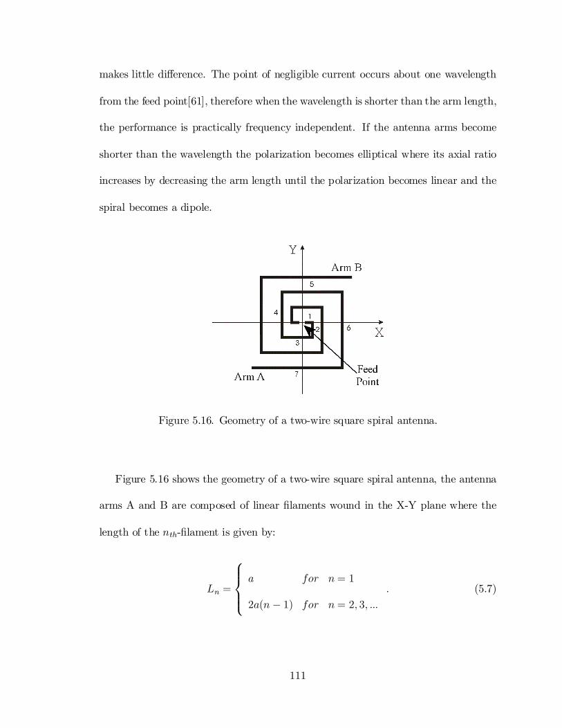
CHAPTER FIVE: COMPARISON OF DIPOLE, BOWTIE, SPIRAL AND LOG-PERIODIC IR ANTENNAS.........................................................................92
CHAPTER SIX: ANTENNA-COUPLED IR PIXELS.....................................122
6.1 2D Array of Antenna-Coupled Microbolometers. ............................123 6.1.1 Antenna Array Theory..........................................................123 6.1.2 Element Spacing.....................................................................125 6.1.3 Response and Noise analysis ................................................128 6.1.4 Experimental Results ............................................................129
6.2 Fresnel Zone Plate Lens .......................................................................138 CHAPTER SEVEN: INTEGRATION TO COMMERCIAL READOUT INTEGRATED CIRCUITS...................................................................................148 CHAPTER EIGHT: CONCLUSIONS AND FUTURE WORK......................156 LIST OF REFERENCES.......................................................................................162
viii
LIST OF FIGURES
1.1 Transmission of the atmosphere ...........................................................................3
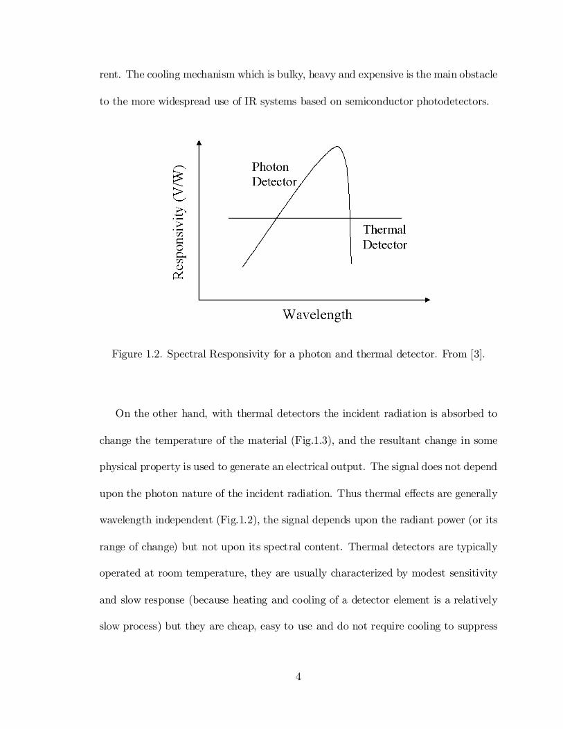
1.2 Relative spectral responsivity for a photon and thermal detector ..................4
1.3 Thermal detector mounted via lags to heat sink ...............................................5
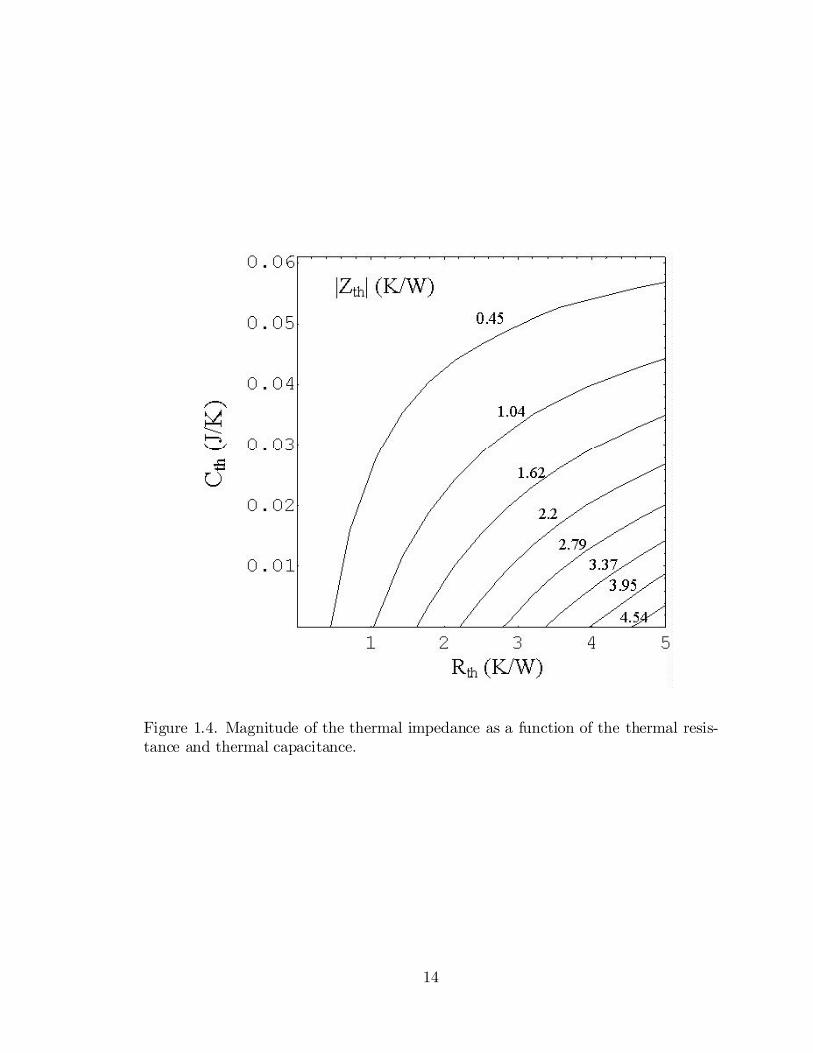
1.4 Magnitude of the thermal impedance as a function of the thermal resistance
and thermal capacitance...............................................................................................14
1.5 Bolometer used in a commercial infrared imaging system................................15
1.6 E¤ective permittivity as a function of substrate thickness ..............................18
1.7 Log-periodic and spiral antenna coupled to a Nb microbolometer..................22
microstrip-patch [27], because of advantages in increased directivity, along with the
possibility of polarization and wavelength selection obtained by using antennas. Fig-
ure 1.7 shows two di¤erent types of antennas designed to detect 10:6 ¹m radiation
coupled to microbolometers, a log-periodic and a square-spiral antenna which were
patterned using direct-write electron beam lithography and lifto¤.
Figure 1.7. Log-periodic and spiral antenna coupled to a Nb microbolometer.
1.6 Focal Plane Arrays
The objective of focal plane array (FPA) technology is to satisfy the requirement for
very large detector arrays by means of the integrated circuit (IC) approach. This
22
requirement is due to the fact that high density detector con…gurations lead to higher
image resolution as well as greater system sensitivity [2]. The invention and develop-
ment of the charged-coupled-device (CCD) was the technological breakthrough that
initially made this possible. By the mid-1970’s a number of concepts for IR-CCDs
had been explored. Prior to the CCD, the only alternative for large arrays was to
con…gure each detector connected to a single wire (and probably an individual pream-
pli…er) which would all need to be packaged in a small dewar. For a large number of
detectors this would obviously create an unmanageable maze of wires and processing
electronics, and which would also require an unacceptable large cooler because of the
thermal conductance of the wiring harness.
1.6.1 Focal Plane Array Architectures
The principal FPA functions are: photon detection, detector readout, signal process-
ing and output multiplexing. In general an FPA may be classi…ed according to its
architecture as hybrid or monolithic (Fig. 1.8) [3]. In hybrid FPAs detectors and
multiplexers are fabricated on di¤erent substrates and mated with each other by ‡ip-
chip bonding (Fig. 1.9(a)) or loophole interconnection (Fig. 1.9(b)). In this case the
detector material and multiplexer can be optimized independently. Other advantages
of the hybrid FPAs are near-100% …ll factor and increased signal-processing area on
the multiplexer chip.
By using ‡ip-chip bonding, the detector array is typically connected by pressure
23
Figure 1.8. IRFPA ARCHITECTURES. For hybrid arrays: (a) ‡ip-chip; (b) Z-technology. For pseudo-monolithic arrays: (c) XY-addressable. For monolithic arrays:(d) all-silicon; (e) heteroepitaxy-on-silicon; (f) non-silicon (e.g., HgCdTe CCD). From[3].
24
contacts via indium bumps to the silicon multiplex pads. The detector array can be
illuminated from either the frontside (with the photons passing through the transpar-
ent silicon multiplexer) or backside (with photons passing through the transparent
detector array substrate). In general the latter approach is most advantageous as the
multiplexer will typically have areas of metallizations and other opaque regions which
can reduce the e¤ective optical area of the structure.
With loophole interconnection, the detector and the multiplexer chips are glued
together to form a single chip before the detector fabrication. Then the photovoltaic
detector is formed by ion implantation and loopholes are drilled by ion-milling. The
loophole interconnection technology o¤ers more stable mechanical and thermal fea-
tures than that of the ‡ip-chip hybrid architecture.
Figure 1.9. Hybrid IRFPA interconnect techniques between a detector array andsilicon multiplexer: (a) indium bump technique, (b) loophole technique.From [3].
25
In the monolithic approach, some of the multiplexing is done in the detector ma-
terial itself rather than in an external readout circuit. The electronics in charge of
multiplexing and processing the detected signal is usually called the readout inte-
grated circuit or ROIC.
1.6.2 Readout Integrated Circuits (ROICs)
The ROIC reads the photo-current from each pixel of the detector array and outputs
the signal in a desired sequence that is used to form a two-dimensional image. A wide
variety of submicron CMOS-based multiplexers have been designed, enabling fabrica-
tion of high performance advanced focal plane arrays with ultra-low noise suitable for
a broad range of applications. The advantage of CMOS are that existing foundries
which fabricate Application Speci…c Integrated Circuits (ASICs) can be readily used
by adopting their design rules.
After the incoming photon ‡ux is converted into a signal by the detector, it is
coupled into the readout via a detector interface circuit. The input circuit is the
most important part of the ROIC because it interfaces directly to the detector, this
input circuitry generally requires that the impedance of the detector be in the order
of 10¡ 100 k to reduce the power dissipation of the whole circuit and also to make
the ROIC detector-noise-limited.
26
CHAPTER 2
DEVICE FABRICATION
The fabrication process of infrared detectors for imaging applications should be com-
patible with modern IC fabrication technology so that monolithic integration into
commercially available readout integrated circuits (ROIC’s) would be possible. Inte-
gration of IR detectors into an FPA would make an IRFPA which is the basic building
block of an infrared imaging system.
2.1 Lithography
Lithography is the cornerstone of modern integrated circuit (IC) manufacturing. The
ability to print patterns with submicron features and to position those patterns on
a silicon substrate with better than 0:1 ¹m precision is what makes integrated cir-
cuits possible. Figure 2.1 shows a schematic of a basic lithographic exposure system.
The lithographic process starts by spinning a light-sensitive photoresist onto a wafer
forming a thin layer on the surface. The resist is then selectively exposed by shining
light through a mask (reticle) which contains the pattern information for the partic-
ular layer being fabricated, this exposure process modi…es the resist making it more
27
(positive resist) or less (negative resist) soluble to a developer. After the develop-
ment process resist will remain in some areas and be removed from some other areas
resembling the mask pattern. The process of transfering the pattern to the wafer
can be done by removing areas (etching), adding materials (deposition) or modifying
the characteristics of the wafer (implantation or di¤usion), the pattern transfer takes
place by having some areas protected with photoresist and other areas exposed to
these processes.
Figure 2.1. Schematic of a simple lithographic exposure system.
28
The photoresists used in IC fabrication normally have three components: a resin
or base material, a photoactive compound (PAC), and a solvent that controls the
mechanical properties, such as viscosity. In positive resists, the PAC acts as an
inhibitor before exposure, slowing the rate at which the resist will dissolve when
placed in a developing solution. Upon exposure to light, a chemical process occurs by
which the inhibitor becomes a sensitizer, increasing the dissolution rate of the resist.
The performance of a resist is measured in sensitivity and resolution, sensitivity refers
to the amount of luminous energy (usually measured in mJ=cm2) necessary to create
the chemical change described above. Resolution refers to the smallest feature that
can be reproduced in a photoresist. The most popular resists are referred to as DQNs,
corresponding to the photoactive compound based on diazoquinones (DQs) and the
matrix material novolac (N) which dissolves easily in an aqueous solution. Solvents
are added to the resin to adjust the viscosity, which is an important parameter for
spin-coating the resist to the wafer. Most of the solvent is evaporated from the resist
before the exposure is done and so plays little part in the actual photochemistry. One
of the great advantages of DQN resists is that they have very good resolution since
the unexposed areas are essentially unchanged by the developer because it does not
penetrate the resist. Another advantage is that novolac is fairly resistant to chemical
attack, being a good mask for subsequent plasma etching. Negative photoresists swell
during the development phase, broadening the linewidth. An after-develop bake will
typically cause the lines to return to their original dimension, but this swelling and
29
shrinking process often causes the lines to be distorted. As a result, negative resists
are generally not suited to features less than 2:0 ¹m.
The most common type of optical source for photolithography is the high-pressure
mercury-xenon arc lamp. Arc lamps are the brightest incoherent sources available,
they emit light from a compact region a few millimeters in diameter, and have total
emissions from about 100 to 2000 W. A large fraction of the total power emerges as
infrared and visible light energy, which must be removed from the optical path with
multilayer dielectric …lters. The useful portion of the spectrum consists of several
bright emission lines in the near ultraviolet and a continuous emission spectrum in
the deep ultraviolet. Because of their optical dispersion, refractive lithographic lenses
can use only a single emission line, either the g line at 425:83 nm, the h line at 404:65
nm, or the i line at 365:48 nm. Each of these lines contains less than 2% of the total
power of the arc lamp.
Because of di¤racion e¤ects there is a resolution limit in lithographic projection
systems given by Rayleigh’s criteria,
D = k1¸NA
(2.1)
whereD is the minimum dimension that can be printed, ¸ is the exposure wavelength,
and NA is the numerical aperture of the optical system. The proportionality constant
k1 is a dimensionless number in an approximate range from 0:6 to 0:8. The resolution
of optical lithography using mercury arc lamps is about 0:5 ¹m.
30
2.2 E-beam Lithography
In chapter 1 we saw that decreasing the size of a bolometer will optimize its respon-
sivity, electron beam lithography (EBL) is a specialized technique for creating the
extremely …ne patterns required for antenna-coupled infrared detectors. It is also
used to generate masks for optical lithography, and for low-volume manufacture of
ultra-small features for high-perfomance devices[28].
Derived from the early scanning electron microscopes, the EBL technique consists
of scanning a beam of electrons across a surface covered with a resist …lm sensitive
to those electrons, thus depositing energy in the desired pattern in the resist …lm.
The process of forming the beam of electrons and scanning it across a surface is
very similar to what happens inside a common television or cathode ray tube (CRT)
display, but EBL typically has three orders of magnitude better resolution. The main
attributes of the technology are:
² It is capable of very high resolution;
² It is a ‡exible technique that can work with a variety of materials and an almost
in…nite number of patterns;
² It is slow, being one or more orders of magnitude slower than optical lithography;
and
² The machinery required is expensive and complicated.
31
Figure 2.2 shows a block diagram of a typical electron beam lithography tool. The
column is responsible for forming and controlling the electron beam.
Figure 2.2. Block diagram showing the major components of a typical electron beamlithography system. From [29].
Underneath the column is a chamber containing a stage for moving the sample
around and facilities for loading and unloading it. Associated with the chamber is
a vacuum system needed to maintain an appropriate vacuum level throughout the
machine and also during the load and unload cycles. A set of control electronics
32
supplies power and signals to the various parts of the machine. Finally, the system
is controlled by a computer, which may be anything from a personal computer to a
mainframe. The computer handles such diverse functions as setting up an exposure
job, loading and unloading the sample, aligning and focusing the electron beam,
and sending pattern data to the pattern generator. The part of the computer and
electronics used to handle pattern data is sometimes referred to as the data path[29].
One of the major areas of concern for electron beam lithography is pattern dis-
tortion due to proximity e¤ects. This refers to the tendency of scattered electrons
to expose nearby areas that may not be intended for exposure. There are several
techniques to minimize the proximity e¤ect, the most popular one is dose correction,
were the dose is varied in such a way as to deposit the same energy density in all
exposed regions of the pattern. Another way of correcting the proximity e¤ect is
shape correction, were the width of lines are decreased and spacings between them
are increased to compensate for the widening of features due to the proximity e¤ect.
The magnitude of these corrections are obtained empirically from test exposures. For
this reason this technique is generally applied only to simple, repetitive patterns or
else this process would turn to be too time consuming. Also the use of beam ener-
gies much greater than 20 keV (e.g., 50 keV) reduces the proximity e¤ect, because
at higher energies the electrons are scattered into a considerably larger region giving
rise to a lower concentration of scattered electrons in the pattern region.
The fabrication of the antenna-coupled infrared detectors described in this study
33
was done at the Cornell Nanofabrication Facility (Ithaca, NY), using a Cambridge
EBMF 10.5 Electron Beam Lithography System at a 30kV accelerating voltage, which
is capable of a resolution of about 150 nm.
2.3 E-Beam Resist Processing
Electron beam resists are the recording and transfer media for e-beam lithography.
The usual resists are polymers dissolved in a liquid solvent. Liquid resist is dropped
onto the substrate, which is then spun at 1000 to 6000 rpm to form a coating. After
baking out the casting solvent, electron exposure modi…es the resist, leaving it either
more soluble (positive) or less soluble (negative) in developer. This pattern is trans-
ferred to the substrate either through an etching process (plasma or wet chemical) or
by “lifto¤” of material. In the lifto¤ process a material is evaporated from a small
source onto the substrate and resist, as shown in Figure 2.3. The resist is washed
away in a solvent such as acetone. An undercut resist pro…le aids in the lifto¤ process
by providing a clean separation of the material. As a rule of thumb the thickness
of the resist should be at least 3£ the thickness of the metallic …lm to get the best
results using lifto¤.
Polymethyl methacrylate (PMMA) was one of the …rst materials developed for
e-beam lithography. It is the standard positive e-beam resist and remains one of
the highest-resolution resists available. PMMA is usually purchased in two high
molecular weight forms (496 K or 950 K) in a casting solvent such as chlorobenzene
34
Figure 2.3. Lifto¤ Process. (a) PMMA is spun on top of copolymer P(MMA-co-MAA) and developed in MIBK:IPA giving a slight undercut. (b) Metal is evaporatedand resist is removed using a liquid solvent, transfering the pattern to the substrate.From [29].
35
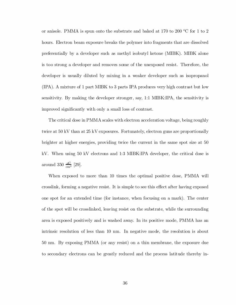
or anisole. PMMA is spun onto the substrate and baked at 170 to 200 oC for 1 to 2
hours. Electron beam exposure breaks the polymer into fragments that are dissolved
preferentially by a developer such as methyl isobutyl ketone (MIBK). MIBK alone
is too strong a developer and removes some of the unexposed resist. Therefore, the
developer is usually diluted by mixing in a weaker developer such as isopropanol
(IPA). A mixture of 1 part MIBK to 3 parts IPA produces very high contrast but low
sensitivity. By making the developer stronger, say, 1:1 MIBK:IPA, the sensitivity is
improved signi…cantly with only a small loss of contrast.
The critical dose in PMMA scales with electron acceleration voltage, being roughly
twice at 50 kV than at 25 kV exposures. Fortunately, electron guns are proportionally
brighter at higher energies, providing twice the current in the same spot size at 50
kV. When using 50 kV electrons and 1:3 MIBK:IPA developer, the critical dose is
around 350 ¹Ccm2 [29].
When exposed to more than 10 times the optimal positive dose, PMMA will
crosslink, forming a negative resist. It is simple to see this e¤ect after having exposed
one spot for an extended time (for instance, when focusing on a mark). The center
of the spot will be crosslinked, leaving resist on the substrate, while the surrounding
area is exposed positively and is washed away. In its positive mode, PMMA has an
intrinsic resolution of less than 10 nm. In negative mode, the resolution is about
50 nm. By exposing PMMA (or any resist) on a thin membrane, the exposure due
to secondary electrons can be greatly reduced and the process latitude thereby in-
36
creased. PMMA has poor resistance to plasma etching, compared to novolac-based
photoresists. Nevertheless, it has been used successfully as a mask for the etching of
silicon nitride and silicon dioxide, with 1:1 etch selectivity[29].
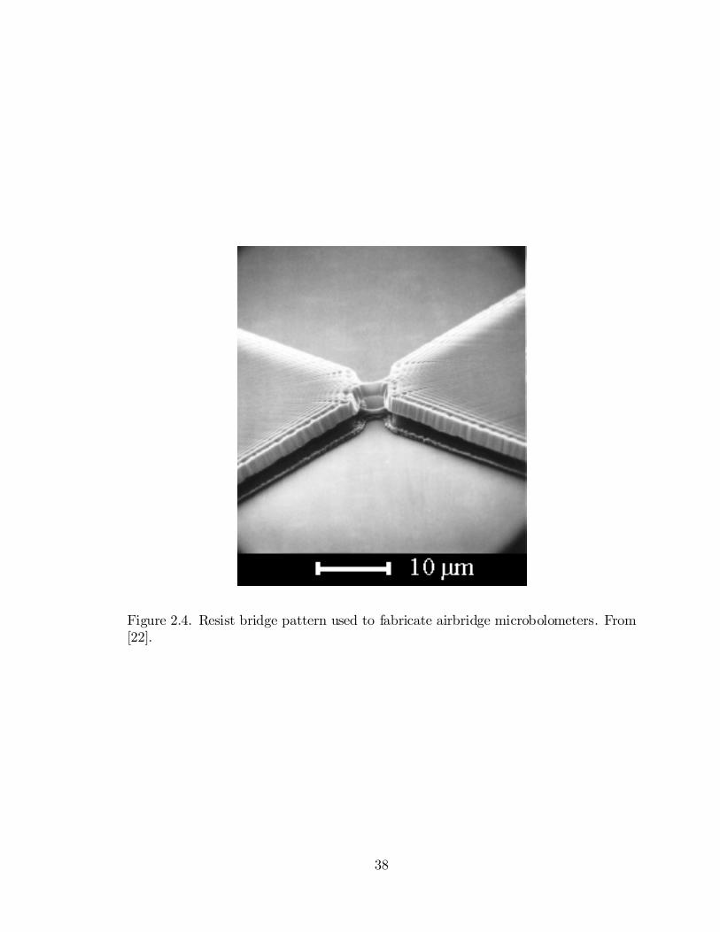
A larger undercut resist pro…le is often needed for lifting o¤ thicker metal layers.
One of the …rst bilayer systems was developed by Hatzakis[30]. In this technique a
high sensitivity copolymer of methyl methacrylate and methacrylic acid [P(MMA-
MAA)] is spun on top of PMMA. A more common use of P(MMA-MAA) is as the
bottom layer, with PMMA on top. In this case the higher speed of the copolymer
is traded for the higher resolution of PMMA.The undercut of this process is so large
that it can be used to form free-standing bridges of PMMA (Figure 2.4).
2.4 Thin Film Deposition Techniques
2.4.1 Evaporation
The metal layers for all of the early semiconductor technologies were deposited by
evaporation, which has been displaced by sputtering in most silicon technologies for
two reasons. The …rst is the ability to cover surface topology, also called the “step
coverage.” Evaporated …lms have very poor ability to cover height discontinuities,
often becoming discontinuous on the vertical walls. It is also di¢cult to produce well
controlled alloys by evaporation. In some cases, the poor step coverage of evaporation
can be used to advantage. Rather than depositing and etching metal layers, the …lm
is deposited on top of a patterned photoresist layer. The …lms naturally tend to break
37
Figure 2.4. Resist bridge pattern used to fabricate airbridge microbolometers. From[22].
38
at the edges of the resist so that when the resist is subsequently dissolved the layer
on top of the resist is easily lifted-o¤ (Figure 2.3)[31].
In an evaporator the wafers are loaded into a high vacuum chamber that is com-
monly pumped with either a di¤usion pump or a cryopump. Di¤usion pumped sys-
tems commonly have a cold trap to prevent the backstreaming of pump oil vapors into
the chamber. The charge or material to be deposited is loaded into a heater container
called the “crucible”. It can be heated very simply by means of an embeded resis-
tance heater and an external power supply or by usign an electron-beam gun. As the
material in the crucible becomes hot, the charge gives o¤ a vapor. Since the pressure
in the chamber is much less than 1 mtorr, the atoms of the vapor travel across the
chamber in a straight line until they strike a surface where they accumulate as a …lm.
Evaporation systems may contain several crucibles to allow the deposition of multi-
ple layers without breaking vacuum. To help start and stop the deposition mechanical
shutters are used in front of the crucibles, and crystal monitors are used to control
the thickness of the deposited metal …lm.
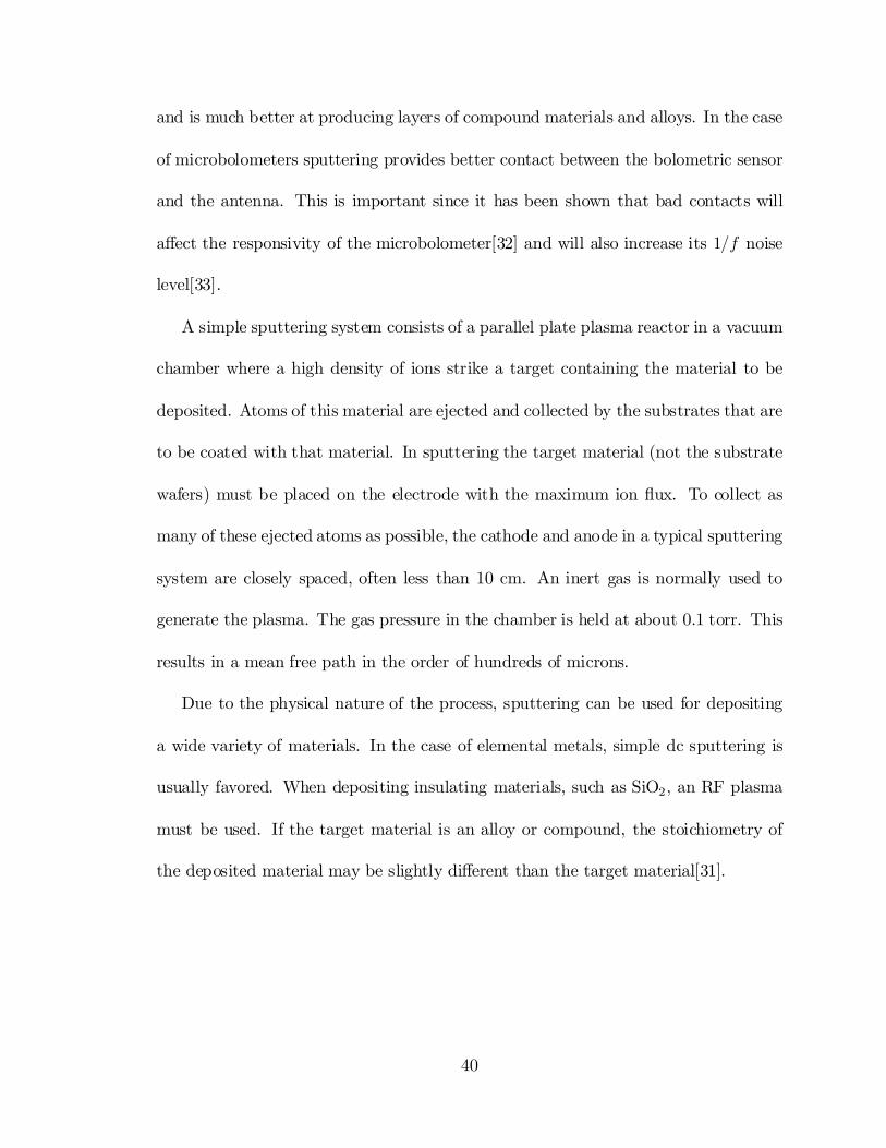
2.4.2 Sputtering
Sputtering is the primary alternative to evaporation for metal …lm deposition in
microelectronics fabrication. First discovered in 1852, sputtering was developed as a
thin …lm deposition technique by Langmuir in the 1920s. It has better step coverage
than evaporation, induces far less radiation damage than electron beam evaporation,
39
and is much better at producing layers of compound materials and alloys. In the case
of microbolometers sputtering provides better contact between the bolometric sensor
and the antenna. This is important since it has been shown that bad contacts will
a¤ect the responsivity of the microbolometer[32] and will also increase its 1=f noise
level[33].
A simple sputtering system consists of a parallel plate plasma reactor in a vacuum
chamber where a high density of ions strike a target containing the material to be
deposited. Atoms of this material are ejected and collected by the substrates that are
to be coated with that material. In sputtering the target material (not the substrate
wafers) must be placed on the electrode with the maximum ion ‡ux. To collect as
many of these ejected atoms as possible, the cathode and anode in a typical sputtering
system are closely spaced, often less than 10 cm. An inert gas is normally used to
generate the plasma. The gas pressure in the chamber is held at about 0.1 torr. This
results in a mean free path in the order of hundreds of microns.
Due to the physical nature of the process, sputtering can be used for depositing
a wide variety of materials. In the case of elemental metals, simple dc sputtering is
usually favored. When depositing insulating materials, such as SiO2, an RF plasma
must be used. If the target material is an alloy or compound, the stoichiometry of
the deposited material may be slightly di¤erent than the target material[31].
40
2.4.3 Chemical Vapor Deposition (CVD)
Evaporation and sputtering are two types of “physical vapor deposition” where phys-
ical methods are used to produce the constituent atoms which pass through a low-
pressure gas phase and then condense on the substrate. In the case of CVD, reactant
gases are introduced into the deposition chamber, and chemical reactions between
them on the substrate surface are used to produce the …lm. CVD has historically
been used in the integrated circuit industry mainly for silicon and dielectric deposi-
tion, primarily due to its good quality …lms and good step coverage.
The materials usually deposited using CVD are silicon in the polycrystalline form
(polysilicon), silicon nitride and phosphor silicate glass (PSG). Polysilicon has prop-
erties comparable to single crystalline silicon, and silicon nitride is a very hard, chem-
ically inert and strong, but brittle material with small thermal conductivity, PSG is
mainly used as a sacri…cial layer for silicon micromachining.
There are three types of CVD, atmospheric pressure CVD (APCVD), low pres-
sure CVD (LPCVD) and plasma enhanced CVD (PECVD). LPCVD has better step
coverage and the mechnical and chemical quality of the …lm (in terms of impurities,
pinholes and density) is much better than APCVD. Films that will be part of mechan-
ical microstructures should be free of internal stresses or else bending and buckling
will occur. The stress of a …lm grown on top of a substrate is indicated with respect
to the underlying material. An expanding layer is then said to be under compressive
stress, a contractive layer under tensile stress[34]. Bending and buckling will occur if
41
the …lm is under compressive stress. Low stress nitride …lms can be deposited in an
LPCVD reactor at 835 oC. PECVD is used when the deposition needs to be done at
low substrate temperatures (» 300 oC) this deposition method has good step coverage
but the …lms su¤er from pinholes and a high hydrogen concentration making them
less suitable for mechanical microstructures.
2.5 Etching
After thin …lms are deposited on the wafer surface, they can be selectively removed
by etching to leave the desired pattern on the wafer surface. In addition to deposited
…lms, parts of the silicon substrate itself may be etched, such as in creating trenches
in isolation structures. The masking layer may be photoresist, or it may be another
thin …lm such as silicon dioxide or silicon nitride. Oxide or nitride masks stand up
better than photoresist to etching conditions and are often called hard masks. But
they themselves must be selectively etched, usually using lithographically de…ned
photoresist as the masking layer. The etching of a thin …lm is usually done until a
di¤erent layer (known as “etch stop”) is reached underneath.
Etching can be done in either a “wet” or “dry” environment. Wet etching involves
the use of liquid etchants. The wafers are immersed in the etchant solution and the
exposed material is etched mostly by chemical processes. Dry etching involves the
use of gas-phase etchants in a plasma. Here the etching usually takes place by a
combination of chemical and physical processes. Because a plasma is involved, dry
42
etching is usually called “plasma etching”[35]. Both methods can be either isotropic,
i.e., provide the same etch rate in all directions, or anisotropic, i.e., provide di¤erent
etch rates in di¤erent directions (Figure 2.5). The important criteria for selecting a
particular etching process are the material etch rate, the selectivity to the material to
be etched versus other materials, and the isotropy/anisotropy of the etching process.
Wet etching provides a good etch selectivity and is usually isotropic with the ex-
ception of anisotropic silicon wet etch using potassium hydroxide (KOH). Dry etching
is often anisotropic, resulting in a better pattern transfer, as mask underetching is
avoided (Figure 2.5). Reactive ion etching (RIE) is a common form of dry etching
where reactive ions are generated in a plasma and accelerated towards the surface to
be etched, this process is anisotropic but has low etch selectivity.
43
2.6 Silicon Micromachining
Silicon micromachining is a process used to fabricate static and movable 3D mi-
crostructures, such as bridges, cantilevers and membranes on silicon substrates. There
are two types of silicon micromachining, bulk micromachining and surface microma-
chining. In the case of bulk micromachining wet-etch and dry-etch techniques are
used to remove parts of the silicon substrate and form the microstructure, whereas
in the case of surface micromachining the microstructure is made of thin-…lm lay-
ers which are deposited on top of the substrate and selectively removed in a de…ned
sequence.
Surface micromachining has become the major fabrication technology of microscale
structures because it uses standard CMOS fabrication processes and facilities. The
most commonly used surface micromachining process is sacri…cial-layer etching. In
this process a microstructure is released by removing a sacri…cial thin-…lm material
which was previously deposited underneath the microstructure (Figure 2.6).
Usually the sacri…cial layer is made out of silicon dioxide (SiO2), phosphorous-
doped silicon dioxide (PSG), or silicon nitride (Si3N4) and the structural layers are
then typically formed with polysilicon, metals and alloys. There are three key chal-
lenges in fabricating microstructures using surface micromachining: control and min-
imization of stress and stress gradient in the structural layer to avoid bending or
buckling of the released microstructure; high selectivity of the sacri…cial layer etchant
to structural layers and silicon substrate; and avoidance of stiction of the suspended
44
Figure 2.6. Surface micromachining fabrication process. (a) Deposition and pattern-ing of the sacri…cial layer. (b) Deposition and patterning of the structural layer. (c)Release etch.
45
microstructure to the substrate[36].
Stiction is the tendency of the suspended structures to collapse due to the sur-
face tension of liquids during evaporation. The liquid forms a droplet during drying
between the microstructure and the substrate which generates an underpressure that
will make the structure collapse if it is not sti¤ enough (Figure 2.7).
Figure 2.7. Capillary force during sacri…cial layer etch.
Rinsing procedures like critical point drying or freeze drying can be used to avoid
stiction. Critical point drying works by exchanging the rinsing liquid, after etching the
sacri…cial layer, with liquid carbon dioxide which is then removed in its supercritical
state avoiding the liquid-gas phase transition. Another alternative to avoid stiction
is to introduce some roughness to the structure or use an anti-stiction coating.
46
2.7 Typical Fabrication Process for Antenna-coupled
Microbolometers
Most of the antenna-coupled microbolometers in this study were patterned on 3-inch,
380 ¹m thick high resistivity (½ ¼ 3 k ¢ cm) silicon substrates, with 200 nm of
thermally or PECVD grown SiO2 for thermal and electrical isolation. The substrates
were spin-coated with a bilayer of copolymer (PMMA-MAA) and PMMA. A 300 nm
layer of 11% copolymer diluted 3:1 in anisole was obtained by spin coating at 3000
rpm for 60 seconds and baking on a hotplate at 170 oC for 15 minutes. A second layer
150 nm thick of 4% PMMA was spun onto the substrate at 3500 rpm for 1 minute
and baked afterwards for 15 minutes on a 170 oC hotplate. The total thickness of the
bilayer was measured with a pro…lometer and was always close to 450 nm.
The antenna, microbolometer patch, bond-pads and bias lines were patterned
using a Cambridge EBMF 10.5 Electron Beam Lithography System at a beam energy
of 40 keV. The dose used for each exposure depended on the critical dimension of the
pattern to write, the antennas and the bias lines were written at the same dose and
with the same beam current, which varied from 150 ¹Ccm2 for the square-spiral antennas
to 250 ¹Ccm2 for bowties. All the antennas were written using 1 nA of beam current. The
bolometer patch was always written at a dose of 350 ¹Ccm2 and 1 nA of beam current.
The bondpads, being large structures (squares of 200 ¹m each side) that took a long
time to write, were written with an e-beam current of 35 nA at a dose of 180 ¹Ccm2
to decrease the exposure time. A wafer with 200 devices (antennas and bondpads)
47
took around 90 minutes to expose. After exposure, the devices were developed for
2 minutes on a 1:1 solution of MIBK:IPA, rinsed with IPA and blow-dried with a
nitrogen gun.
The antennas were made out of 100 nm of e-beam evaporated gold over a 5 nm
adhesion-layer of Cr and lifto¤ was done by soaking the wafers on methylene chloride
for 2 hours. The microbolometers were made o¤ a thin …lm (» 70 nm) of RF-sputtered
VOx or DC-sputtered Nb, and the lifto¤ process was done using methylene chloride
also.
To increase the thermal isolation of the microbolometers some of them were fab-
ricated on a silicon nitride membrane using surface micromachining. The antenna-
coupled microbolometer was patterned on a silicon substrate with 3 ¹m of thermally
grown SiO2 and 400 nm of low-stress Si3N4 deposited using LPCVD. The silicon ni-
tride membrane was patterned using CF4-based RIE and released by etching the SiO2
sacri…cial layer with hidro‡uoric acid (HF 49% in water) and critical point drying.
48
CHAPTER 3
CHARACTERIZATION OF ANTENNA-COUPLED
DETECTORS
Infrared radiation is collected by an antenna by the generation of current in its ele-
ments, this generated current has the same frequency as the incident radiation, in the
infrared case the frequency would be in the 30 terahertz range. This generated current
will ‡ow through the sensing element, in this case the bolometer, and will increase its
temperature by joule heating. The change in temperature will make the bolometer
change its resistance, thus providing the detection mechanism. Other advantages of
using an antenna as collection element are directivity, polarization dependence and
tunability.
Antenna-coupled infrared detectors were fabricated using electron-beam lithog-
raphy and lifto¤ on 3-inch silicon wafers, Figure 3.1 shows a dipole-coupled mi-
crobolometer fabricated using this method. Each processed wafer was scribed into 1
cm £ 1 cm die with 10 devices each and bonded on chip carriers specially made to
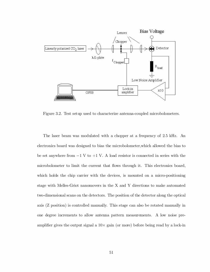
The test setup that was used to characterize antenna-coupled infrared detectors
is shown in Figure 3.2. A CO2 laser emitting infrared radiation at 10.6 ¹m focused
using an F/8 optical train was used, the resulting spot can be seen in Figure 3.3.
The diameter of the spot that encloses 84% of the ‡ux in the di¤raction pattern
is approximately 200 ¹m, the power at the focal plane was set using a wire-grid
polarizer, most of the measurements were made at 33 mW of optical power at the
focal plane, which gives an approximate irradiance of 88 W=cm2 at the focus. The
optical train includes a half wave plate which is used to rotate the linear polarization
of the CO2 laser.
50
Figure 3.2. Test setup used to characterize antenna-coupled microbolometers.
The laser beam was modulated with a chopper at a frequency of 2.5 kHz. An
electronics board was designed to bias the microbolometer,which allowed the bias to
be set anywhere from ¡1 V to +1 V. A load resistor is connected in series with the
microbolometer to limit the current that ‡ows through it. This electronics board,
which holds the chip carrier with the devices, is mounted on a micro-positioning
stage with Melles-Griot nanomovers in the X and Y directions to make automated
two-dimensional scans on the detectors. The position of the detector along the optical
axis (Z position) is controlled manually. This stage can also be rotated manually in
one degree increments to allow antenna pattern measurements. A low noise pre-
ampli…er gives the output signal a 10£ gain (or more) before being read by a lock-in
51
ampli…er using the chopper frequency as reference.
Figure 3.3. Two dimensional scan of the F/8 beam used to characterize antenna-coupled bolometers. Contours are drawn at 20% intervals.
52
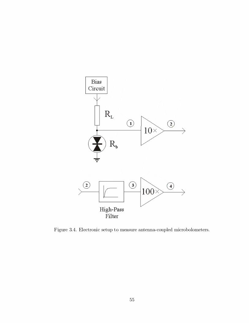
3.1 Low Noise Ampli…er Design
In order to have an accurate value for the signal-to-noise ratio of antenna-coupled
microbolometers the noise level of the measurement system should be small compared
to the noise of the device under test. Figure 3.4 shows a schematic representation of
the ampli…cation stages used to measure the noise and response of microbolometers.
By using ampli…cation stages the noise level of the measurement equipment relative
to the noise of the detector gets reduced, for example amplifying the output signal
1000£ will make the noise of the measurement equipment appear 1000£ lower in
comparison. This will give a more accurate reading, however the ampli…cation stages
introduce some additional noise to the system which needs to be small compared to
the noise of the detector. Two ampli…cation stages and a high-pass …lter are needed
if ampli…cations higher than 100£ are desired or else the dc-bias voltage (which is
usually around 100 mV) will saturate the ampli…cation stage. The noise contribution
of the …lter will be reduced if its placed after the …rst ampli…cation stage. The noise
analysis of the circuit shown in Fig. 3.4 proceeds as follows: the noise at point 1 (n1)
is given by the noise of the bias voltage (nbias) divided by the voltage divider formed
by RL and Rb plus the noise of the bolometer (nb) added in quadrature:
n1 =
sµnbiasRbRb + R1
¶2
+ n2b: (3.1)
53
The noise at point 2 (n2) is given by the noise at point 1 ampli…ed by 10£ plus the
noise of the ampli…cation stage (n10£) added in quadrature,
n2 =q
(10 ¢ n1)2 + n210£: (3.2)
If more than one stage of ampli…cation is required, a high-pass …lter should be used
betwen the ampli…cation stages. For a …rst-order high-pass …lter the noise at point 3
(n3) will be given by the noise at point 2 (n2) plus the addition in quadrature of the
Johnson noise of the resistor used in the high-pass …lter (RHP ),
n3 =pn22+ 4kTRHP ; (3.3)
where k is the Boltzmann constant and T is absolute temperature. The noise at point
4 (n4) is given by the noise at point 3 ampli…ed by the gain of the second amplifying
stage plus the noise of the ampli…cation stage (n100£) added in quadrature,
n4 =q
(100 ¢ n3)2 + n2100£: (3.4)
The total noise of the system referred to the input is the total noise at the output
divided by the total ampli…cation, that is: nT = n4=1000.
The total noise in the circuit shown in Fig. 3.4 can be reduced by making the noise
contributions of the bias voltage and the ampli…cation stages as small as possible.
Figure 3.5 shows the bias circuit used, the use of batteries and decoupling capacitors
54
Figure 3.4. Electronic setup to measure antenna-coupled microbolometers.
55
along with an ultralow noise op-amp (TL1028) helped reduce the noise of the bias
voltage to 7 nVpHz
at 100 Hz. The bias circuit in Fig. 3.5 gives a 1V …xed output which
will be reduced to the desired bias voltage by resistor RL from Fig. 3.4, a …xed bias
voltage was chosen to avoid the high 1=f noise level of potentiometers. Decoupling
capacitors are used to reduce the high frequency noise in the system. Batteries power
the op-amp and are used instead of regulated power supplies due to their lower noise.
Figure 3.5. Low-noise bias source for microbolometers.
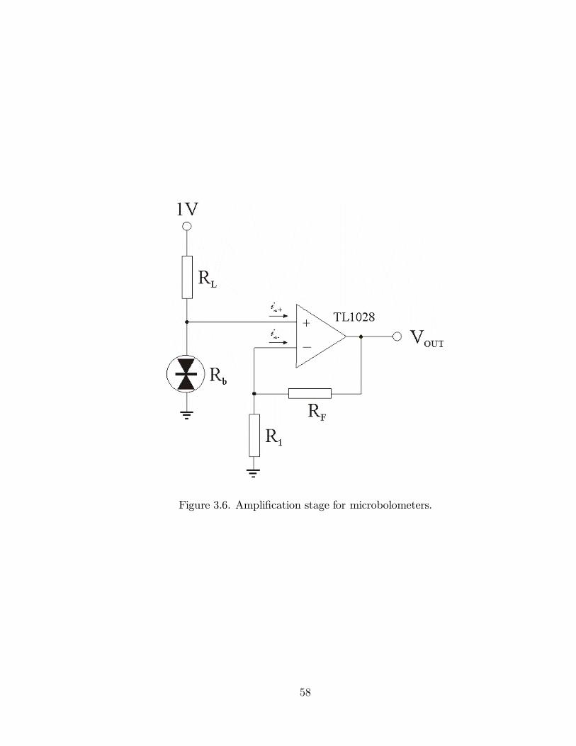
Figure 3.6 shows an ampli…cation stage for microbolometers with a gain given
by (RFR1 + 1): The noise analysis for this circuit can be obtained by superposition
and adding the individual noise contributions in quadrature. The noise contribu-
tion of the op-amp comes from two sources, its voltage noise and its current noise
which are parameters than can be found in the op-amp’s data sheet or measured
56
directly. The voltage noise contribution is given by nopamp, which can generally be
found in the opamp’s datasheet, and the current-noise contribution is the voltage
generated by the current noise ‡owing through external resistors. In the case of
the circuit shown in Fig. 3.6, the current-noise contribution is given by in(RLkRb)
and in(R1kRF). The noise due to the external resistors RL; Rb; RF and R1 is given
byp4kTRL( Rb
RL+Rb);
p4kTRb( RL
RL+Rb);
p4kTRF( R1
RF+R1) and
p4kTR1( RF
RF+R1) respec-
tively. All these expresions for noise voltages are referred to the input, therefore they
have to be multiplied by the gain to get the noise at the output of the ampli…cation
stage. The total noise of the ampli…cation stage, referred to the input, is given by:
n2amp = n2opamp + i2n
·(RbRLRL +Rb
)2 + (R1RFR1+ RF
)2¸
(3.5)
+4kT·RL(
RbRL + Rb
)2 +Rb(RL
RL + Rb)2 +RF (
R1
RF + R1)2+ R1(
RFRF +R1
)2¸:
For a 10£ ampli…cation stage with RF = 499 and R1 = 54:9 with a 200-
bolometer biased at 100 mV (Rb = 200 and RL = 1:8 k) using a TL1028 ultralow
noise op-amp (nopamp = 0:85 nVpHz; in = 1:6 pAp
Hzboth measured at 100 Hz [37]) the
total noise at the output will be given by the contribution of the bias voltage and the
noise of the ampli…cation stage:
ntotal =
sµnbiasRbRb +RL
¶2
+ n2amp: (3.6)
57
Figure 3.6. Ampli…cation stage for microbolometers.
58
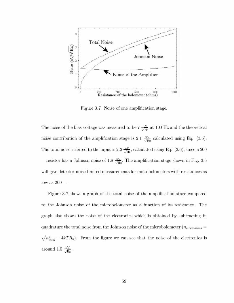
Figure 3.7. Noise of one ampli…cation stage.
The noise of the bias voltage was measured to be 7 nVpHz
at 100 Hz and the theoretical
noise contribution of the ampli…cation stage is 2:1 nVpHz
calculated using Eq. (3.5).
The total noise referred to the input is 2:2 nVpHz; calculated using Eq. (3.6), since a 200
resistor has a Johnson noise of 1:8 nVpHz: The ampli…cation stage shown in Fig. 3.6
will give detector-noise-limited measurements for microbolometers with resistances as
low as 200 .
Figure 3.7 shows a graph of the total noise of the ampli…cation stage compared
to the Johnson noise of the microbolometer as a function of its resistance. The
graph also shows the noise of the electronics which is obtained by subtracting in
quadrature the total noise from the Johnson noise of the microbolometer (nelectronics =pn2total ¡ 4kTRb). From the …gure we can see that the noise of the electronics is
around 1:5 nVpHz:
59
Figure 3.8. Noise Floor of the measuring electronics.
3.2 Noise Measurements
Noise measurements were made using the setup shown in Fig. 3.4 and an HP3562A
Dynamic Signal Analyzer which has a measurement range of 64 ¹Hz to 100 kHz. The
noise introduced by the signal analyzer was attenuated 1000£ referred to the noise of
the detector due to the ampli…cation stages of the test setup. The noise ‡oor of the
test setup was measured by shorting the bolometer. The result is shown in Fig. 3.8,
and we can see that the noise ‡oor is very close to the 1:5 nVpHz
noise expected from the
theoretical noise calculations. The spikes in the measurements are 60Hz power-line
harmonics introduced into the system.
60
Figure 3.9. Noise spectrum for a 200 chrome microbolometer and …tting function.
The noise characteristics of microbolometers depend on the bolometric material
used and its deposition process, Fig. 3.9 shows the noise spectrum of a 200 e-
beam evaporated chrome microbolometer. Devices that are sputtered show lower
noise levels than evaporated bolometers, because sputtering provides a better contact
between the bolometric material and the gold structures, which reduces 1=f noise.
The noise spectrum of a 200 chrome bolometer …ts the following noise function:
nb =100f
+ 70pf+6; (3.7)
which shows two 1=f k components. Figure 3.9 shows the noise spectrum of a 200
chrome bolometer and the …tting function (Eq. (3.7)).
61
3.3 Response Measurements
Response measurements are taken using the test setup shown in Fig. 3.2. For signal-
to-noise (SNR) calculations, noise and response measurements should be taken at the
same level of ampli…cation. The total response of the devices is measured in volts
from the lock-in ampli…er or can also be measured directly from an oscilloscope, in
which case the output would look like a square wave with the same frequency of the
chopper.
The maximum response of the device is measured at the polarization that best
matches the antenna being measured (co-polarized response) and the minimum re-
sponse is taken at the polarization that gives the lowest response (cross-polarized
response), the co-polarized minus the cross-polarized response results in the pure
antenna response. The ratio between the co-polarized and cross-polarized response
gives the polarization ratio of the antenna. The cross-polarized response is usually
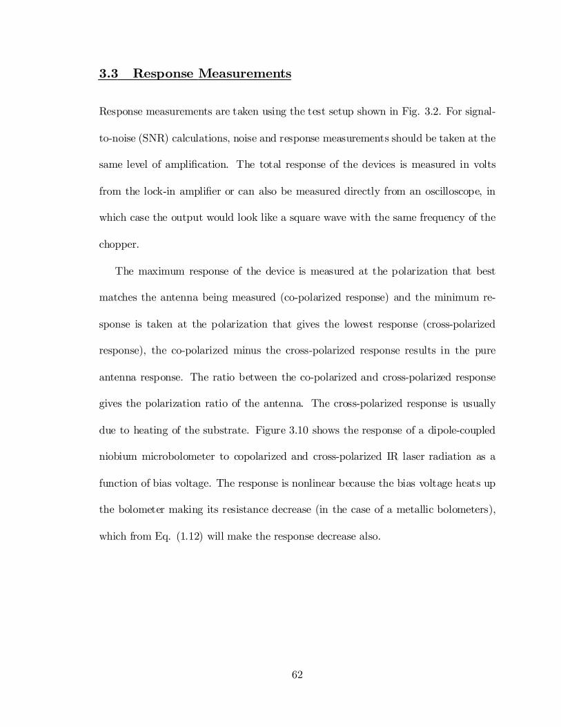
due to heating of the substrate. Figure 3.10 shows the response of a dipole-coupled
niobium microbolometer to copolarized and cross-polarized IR laser radiation as a
function of bias voltage. The response is nonlinear because the bias voltage heats up
the bolometer making its resistance decrease (in the case of a metallic bolometers),
which from Eq. (1.12) will make the response decrease also.
62
Figure 3.10. Response of a dipole-coupled microbolometer as a function of the biasvoltage.
3.4 Polarization Dependence
Polarization is a basic property of antennas. Since bolometers are not sensitive to
polarization, if an antenna-coupled microbolometer shows a change in response due
to a change in polarization then an antenna e¤ect is taking place. This polariza-
tion dependence should match the polarization characteristics of the antenna used to
couple radiation into the microbolometer.
The polarization of the linearly polarized laser beam shown in Fig. 3.2 can be
rotated by using a half-wave plate, a quarter-wave plate can be used if circular polar-
ization is needed. A wave plate is made of a slab of birefringent material that changes
the phase between the two orthogonal components of a linearly polarized wave, if this
phase change is equal to ¼ then the linear polarization of the wave will be rotated,
63
if the phase change is ¼=2 then the resulting wave will be circularly polarized, any
other phase change will give an elliptically polarized wave.
Figure 3.11 shows how the response of a dipole-coupled microbolometer changes
with polarization. Dipoles are linearly polarized antennas and therefore have a cosine-
squared polarization dependence. The measurements shown in Fig. 3.11 …t the
following equation, V = 215cos2(x + 65o) + 74: The polarization ratio in this case is
around 4.
Figure 3.11. Polarization dependence of a dipole-coupled microbolometer.
64
3.5 Time Constant Measurements
To measure the time constant of antenna-coupled microbolometers an acousto-optic
(AO) modulator was incorporated into the optical setup shown in Fig. 3.2 instead
of the mechanical chopper. The AO modulator can modulate the laser beam up
to 10 MHz. Frequencies this high cannot be handled by the ampli…cation stages
therefore the output of the device under test has to go directly to a lock-in ampli…er
or spectrum analyzer. The time constant measurements were taken by varying the
modulation frequency of the AO modulator with an HP 33120A function generator
and measuring the response of the device with an HP 3585 spectrum analyzer. The
measurements were automated using a computer with HPIB interface and software
programmed in Labview.
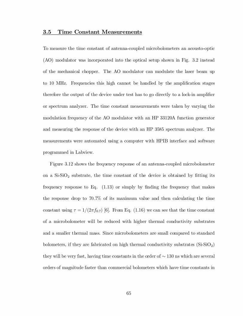
Figure 3.12 shows the frequency response of an antenna-coupled microbolometer
on a Si-SiO2 substrate, the time constant of the device is obtained by …tting its
frequency response to Eq. (1.13) or simply by …nding the frequency that makes
the response drop to 70:7% of its maximum value and then calculating the time
constant using ¿ = 1=(2¼f0:7) [6]. From Eq. (1.16) we can see that the time constant
of a microbolometer will be reduced with higher thermal conductivity substrates
and a smaller thermal mass. Since microbolometers are small compared to standard
bolometers, if they are fabricated on high thermal conductivity substrates (Si-SiO2)
they will be very fast, having time constants in the order of » 130 ns which are several
orders of magnitude faster than commercial bolometers which have time constants in
65
the » 10 ms range. There is a tradeo¤ between speed of the detector and responsivity,
from Eq. 1.13 we can see that fast bolometers (small time constant ¿ ) will have low
responsivity, therefore the substrate material has to be chosen so that the maximum
response can be obtained for the desired detector speed.
Figure 3.12. Time constant of an antenna-coupled microbolometer on a Si-SiO2 sub-strate.
3.6 Radiation Patterns
Another basic property of antennas is their radiation pattern. In the case of antenna-
coupled microbolometers its response as a function of angle of incidence will give the
radiation pattern of the antenna. These antenna patterns are measured by rotating
the stage with respect to the the optical axis in one degree increments and recording
66
the response of the device. After every rotation the X, Y and Z positions have to be
readjusted to center the device at the focus of the laser beam. This is done by adjust-
ing the position of the device until the maximum response of the device is obtained.
The use of high F=# optics (F=8) to focus the CO2 laser on the detector reduces the
e¤ect of the convolution of the antenna pattern with the angular distribution of the
focused light cone.
Figure 3.13 shows the radiation pattern of an array of dipole-coupled microbolome-
ters, it shows the normalized radiation pattern on a linear scale (Fig. 3.13(a)) and
on a dB scale (Fig. 3.13(b)).
Figure 3.13. Radiation Pattern of a 2D-Array of dipole-coupled microbolometers. (a)Linear scale, (b) dB scale.
3.7 Spatial Response of Antenna-Coupled Detectors
The signal obtained by a detector is proportional to the irradiance distribution in-
tegrated over its collection area. Commercial bolometers are much bigger than the
67
wavelength and their collection area can be determined by scaning a probe beam
across the detector and measuring the output of the detector as a function of the po-
sition of the probe. If the dimensions of the detector are large compared to the probe
beam then the detector’s spatial response will be very close to the scanned area that
generated a response. If this method is used with microbolometers we are scanning a
structure smaller than the probe beam, so that a two dimensional scan will result in
the convolution of the beam with the spatial response of the detector. In order to ex-
tract the spatial response a deconvolution of the two-dimensional scan with the laser
beam has to be made. Alda et al. [38] developed a deconvolution method to extract
the spatial response of lithographic infrared antennas from two-dimensional scans by
deconvolving the laser beam, which is modeled as a 2D Gaussian beam convolved with
a slightly comatic Airy function. The analytical beam model is obtained by …tting
the characteristics of the real laser beam obtained by knife-edge measurements.
The two-dimensional scan data is obtained by focusing a 10.6 ¹m CO2 laser beam;
using F=1 optics, on the detector. A serial scan is performed, moving the device in
the X and Y directions using a motorized Melles-Griot Nanomover system, which is
controlled by a computer that also records the response of the detector from the lock-
in ampli…er. Measurements were usually made by scanning a 100 ¹m£ 100 ¹m area
at 1 ¹m steps. This scanning procedure was automated using software programmed
in Labview which also collected the output data. Each measurement took around 1.5
h to acquire. The software saved the response in a two-dimensional matrix format
68
and a program made in Matlab performed the deconvolution using the algorithm
described in [38]. Figure 3.14(a) shows the two-dimensional scan of a log-periodic-
coupled microbolometer and Fig. 3.14(b) shows the results after deconvolution.
Figure 3.14. Spatial response of infrared antennas. (a) Two dimensional scan of alog-periodic antenna, (b) spatial response of log-periodic antenna after deconvolution.
69
CHAPTER 4
MATERIALS FOR ANTENNA-COUPLED IR
DETECTORS
An antenna-coupled microbolometer consists of a metallic antenna, bias lines, a bolo-
metric detector and a substrate. The materials used in the fabrication of antenna-
coupled microbolometers play an important role in their performance. Materials that
provide better thermal isolation, better matching of the IR radiation to the antenna
along with a high-TCR microbolometer will make higher responsivity detectors.
4.1 Substrate Losses and Silicon Lenses
Antennas on a dielectric are most sensitive to radiation from the substrate side[39].
However for an antenna lying on a substrate (Figure 4.1), rays incident on the air-
substrate interface at an angle larger than the critical angle are completely re‡ected
and trapped as surface waves[40] reducing the e¢ciency of the antenna, by reciprocity
this reduction in e¢ciency applies for receiving antennas also. These surface waves
may show up experimentally as spikes in a receiving antenna pattern [11]. The sim-
70
plest way to solve this problem is to mount on the back side of the substrate a lens
with the same dielectric constant, this way the rays are now incident nearly normal
to the surface and do not su¤er total internal re‡ection (Figure 4.2).
Figure 4.1. Trasmitting antenna on a dielectric substrate showing the rays trappedas surface waves. From [40].
The substrate lens takes advantage of the sensitivity of an antenna to radiation
from the substrate side and eliminates the surface waves. The disadvantages are
absorption losses and the di¢culty of optically contacting and aligning the lens to
a lithographic antenna. Hemispherical substrate lenses are particularly attractive
because they are aplanatic, adding no spherical aberration or coma[41]. These lenses
also do not refract the transmitted rays, (Fig. 4.2) a characteristic that makes them
useful for antenna-pattern measurements. A hemisphere has a linear magni…cation
equal to the index of refraction n of the material it is made o¤, increasing the e¤ective
collection area of an infrared detector by a factor of n2.
71
Figure 4.2. Antenna-coupled detector with a Silicon substrate lens.
A 15-mm diameter silicon hemisphere was attached to an antenna-coupled mi-
crobolometer on a Si-substrate. Measurements on these type of devices gave a 15£
increase in response, a bit more than the expected n2£ apparent increase in area of
the detector ( n2 ' 11:7 for silicon at 10:6 ¹m). Figure 4.3 shows the radiation pattern
of a bowtie antenna with and without a silicon hemisphere attached, the radiation
pattern with the silicon hemisphere shows a sharp signal drop for angles of incidence
higher than 15 degrees, this can be explained by total internal re‡ection due to an
air gap between the substrate and the silicon sphere, the critical angle in a silicon-air
interface is around 17 degrees, this e¤ect can be avoided by making optical contact
between the silicon sphere and the substrate or by fabricating the antenna-coupled
detector directly on the silicon sphere.
72
Figure 4.3. Radiation Pattern of a Bowtie Antenna (a) on a silicon substrate, (b)with a hemispherical silicon lens attached.
4.2 VOx microbolometers
From Eq.(1.14) we can see how the temperature coe¢cient of resistance ® (TCR) of
the bolometer is directly proportional to the responsivity of the detector, therefore the
choice of the thin-…lm heat-sensitive material is an important factor in maximizing
the response of microbolometers. A thin …lm of sputtered Nb, which has a reported
TCR close to 0:3 %=K [42], was used as the bolometer in [43]. Vanadium is a metal
with a variable valence forming a large number of oxides which have a very narrow
range of stability[44], …lms of vanadium oxide (VOx) consisting of a mixture of var-
ious oxides present a TCR ¼ 2 %=K and have been used in the past to fabricate
microbolometers[45]. More involved deposition processes have also been reported,
yielding …lms of stoichiometric VO2 with TCR’s greater than 5 %=K [46].
A comparison of the performance between Nb-based and VOx-based microbolome-
ters was performed using two-dimensional arrays of log-periodic-coupled microbolome-
ters with a 50 ¹m£ 50 ¹m pixel area (Figure 4.4). The Nb-based microbolometers
73
showed an average dc resistance of 1.2§0.1 k and the VOx detectors presented
450§50 average dc resistance. The measurements were made at a bias voltage of
300 mV.
Figure 4.4. Scanning Electron micrograph of a 2D array of Log-periodic antenna-coupled detectors.
The response of the antenna arrays to 10.6 ¹m radiation was measured, the Nb-
based detectors gave a co-polarized signal of 5.1§1 ¹V while the measured response
74
of the VOx-based devices was 22.5§2.5 ¹V, which corresponds to a a 4.5£ increase in
response. Figure 4.5 shows the noise frequency spectrum measured with an HP3562A
dynamic signal analyzer. The Nb-based devices had a noise voltage spectrum of
120§10 nV=pHz at 100 Hz while the VOx-based devices presented a noise voltage
spectrum of 60§5 nV=pHz at the same frequency. This represents a 9£ increase in
signal-to-noise ratio of the VOx-based devices over the Nb-based ones.
Figure 4.5. Noise Frequency Spectrum for Nb and VOx based detectors.
Figure 4.6 shows the measured angular patterns of the Nb-based devices and the
VOx based devices, the radiation characteristics for similar antenna array con…gura-
tions show that the impedance at the feed does alter the electromagnetic characteris-
tics of the antenna array, in this particular case the Nb-based array presents a more
directive pattern than the VOx-based detector, which indicates that the impedance
75
of the Nb patch is a better match for the individual log-periodic elements of the array.
The thickness of the VOx bolometer can be varied to better match its impedance to
the antenna elements and get a further increase in response.
Figure 4.6. Radiation Patterns of (a) Nb-based 2D array, and (b) VOx-based 2Darray.
This comparison of antenna-coupled microbolometers with di¤erent bolometric
materials shows that the use of higher TCR materials will increase the response of
the detector, this increase in response will be equal to the ratio of TCR’s only if the
bolometers have the same impedance so that the e¢ciency of the antenna remains
the same. Using di¤erent materials will also change the noise characteristics of the
detector.
An interesting characteristic of vanadium oxide …lms is that they exhibit a metal-
semiconductor phase transition at which the resistivity and re‡ectance sharply changes
76
Figure 4.7. Experimental Resistance vs. Temperature dependence of VO2. From [47].
77
(Fig. 4.7). Single-crystal vanadium dioxide behaves like a semiconductor at temper-
atures below 45 oC and like a metal at temperatures above 67 oC, a change in the
resistance by a factor of 103£ is observed. Figure 4.7 shows a graph of the resis-
tance of VO2 as a function of temperature, TCR is proportional to the slope of the
resistance-versus-temperature curve of the material, during its phase transition the
TCR of VO2 reaches values as high as 200 %=K [48]. This property can be used
to increase the sensitivity of VOx microbolometers. The moderate temperature of
this transition (40-70 oC) can be reached by Joule heating of the sensitive element
by passing a bias current through it with su¢ciently good thermal insulation of the
element. The di¢culties in this method consist of the hysteresis character of the
transition, variable biasing methods have to be implemented to use the large slope of
the R(T) dependence [48] [46].
4.3 Thermal Isolation using Aerogel
From Eqs. (1.14),(1.15) and (1.16) we can see that an increase in the thermal im-
pedance of the detector would increase the responsivity of the detector, but will also
increase its time constant, slowing down the response of the detector and therefore
decreasing its bandwidth. The highest thermal impedance would occur when the de-
tector is completely isolated from the environment, therefore the use of high thermal
conductivity substrates will make a bolometer faster but will reduce its responsivity.
From the above stated we can see that a trade-o¤ exists between responsivity
78
and speed of the detector; in order to fabricate fast detectors low thermal isolation
is required which yields low responsivity, therefore the thermal conductivity of the
substrate has to be chosen so that it gives the maximum response for the required
frame-rate.
Aerogels are materials that consist of pores and particles that are in the nanometer
size range and have exceptional optical, thermal, acoustical and electronic properties[49]
which depend on the porosity of the …lm. Thermal conductivity decreases linearly as
porosity of the aerogel …lm increases, values lower than air have been measured on 70-
99% porosity …lms[50]. Thin aerogel …lms with up to 98% porosity can be deposited
on Si wafers by spin coating or dip coating, and can later be used as substrates for
further lithographic processing[49]. Here the noise, response, time constant and radi-
ation characteristics of two dimensional arrays of antenna-coupled microbolometers
fabricated on aerogel-coated substrates are studied and compared to similar devices
fabricated on Si-SiO2 substrates. Two dimensional arrays of dipole-coupled [Fig.
4.8(a)] and bowtie-coupled [Fig. 4.8(b)] microbolometers were used in this study. A
series con…guration was selected to match the input impedance of typical commercial
ROIC’s which is in the kilo-ohm range[51], and cover a pixel area of 50 ¹m£ 50 ¹m.
Silica aerogel thin …lms were deposited by spin coating onto thermally-oxidized
silicon wafers using the process described by Clem et al. [50]. The resulting …lm was
700 nm thick and had a refractive index of 1.06, as measured by 632 nm ellipsometry,
which indicates that the silica aerogel …lm had a porosity of 85 %[49]. Silica aerogels
There are several problems associated with fabricating standing structures, two
basic problems are thin …lm stress and stiction. There are two types of thin …lm
stress, tensile or compressive lateral stress and stress gradients in the …lm[34], these
forces make the suspended structures buckle (Figure 4.14). The second problem
is stiction. When etching the sacri…cial layer the free-standing structures have the
tendency to collapse, the cause is the surface tension of the liquid during evaporation,
the liquid forms a droplet during drying between the microstructure and the substrate
which generates an underpressure that makes the microstructure collapse. To solve
this problem other rinsing procedures should be used such as critical point drying or
freeze drying.
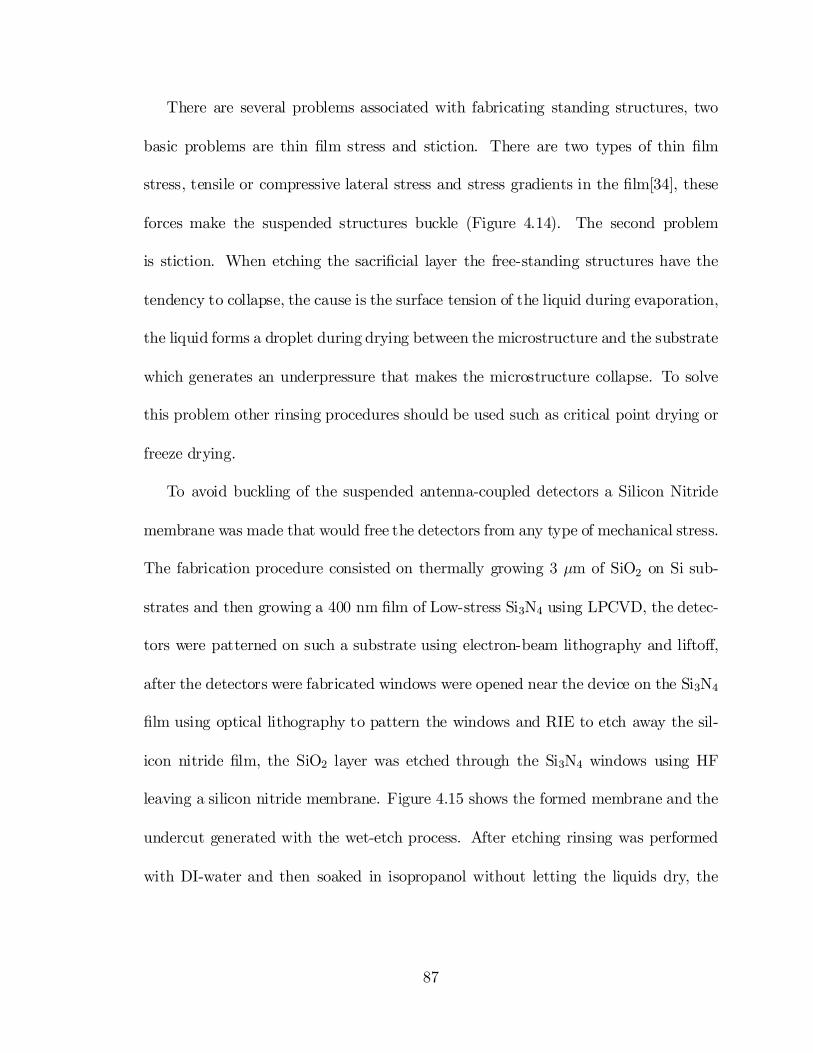
To avoid buckling of the suspended antenna-coupled detectors a Silicon Nitride
membrane was made that would free the detectors from any type of mechanical stress.
The fabrication procedure consisted on thermally growing 3 ¹m of SiO2 on Si sub-
strates and then growing a 400 nm …lm of Low-stress Si3N4 using LPCVD, the detec-
tors were patterned on such a substrate using electron-beam lithography and lifto¤,
after the detectors were fabricated windows were opened near the device on the Si3N4
…lm using optical lithography to pattern the windows and RIE to etch away the sil-
icon nitride …lm, the SiO2 layer was etched through the Si3N4 windows using HF
leaving a silicon nitride membrane. Figure 4.15 shows the formed membrane and the
undercut generated with the wet-etch process. After etching rinsing was performed
with DI-water and then soaked in isopropanol without letting the liquids dry, the
87
Figure 4.14. Buckled bridge structure. From [54].
88
isopropanol was later dried using a critical point drier (CPD) to avoid stiction.
Figure 4.15. Window openings on Si3N4 to build a membrane.
Since HF attacks niobium and other bolometric materials the antenna-coupled
detector was fabricated using gold for the antenna elements and bias line and chrome
as the bolometric material (Figure 4.16).
The square-spiral detectors on membranes were tested under vacuum and without
a vacuum, without a vacuum a responsivity of 144 V=W and a D¤ of 3£ 106 cmpHz
W
89
Figure 4.16. Square-spiral-coupled microbolometer on a silicon nitride membrane.
90
was obtained, under a vacuum the measured responsivity was 224 V=W and a D¤ of
1:7 £ 107 cmpHz
W . Taking into account that Cr has a TCR 30£ lower than VOx, by
fabricating a VOx microbolometer on a membrane, values well above 1 £ 103 V=W
and 1£ 108 cmpHz
W for responsivity and D¤ should be obtained when VOx is used in
a membrane con…guration.
This membrane fabrication process can be modi…ed to allow the use of materi-
als that are attacked by HF by masking them with chrome. After fabricating mi-
crobolometers using HF-sensitive materials a thin layer of chrome is deposited to
protect them from the HF etch. Windows are opened through the chrome and the
silicon nitride layers to allow for the silicon dioxide etch. The following step is to
remove the chrome layer by using chrome etch. This process will allow the use of
materials like titanium, vanadium oxide and niobium on a silicon nitride membrane
using silicon dioxide as the sacri…cial layer.
91
CHAPTER 5
COMPARISON OF DIPOLE, BOWTIE, SPIRAL AND
LOG-PERIODIC IR ANTENNAS
Antenna-coupled microbolometers use planar lithographic antennas to couple incident
radiation into a bolometer with sub-micron dimensions. The use of an antenna limits
the throughput to one mode with one polarization. This limitation to one mode is
potentially useful for bolometers used for di¤raction limited observations over a broad
spectral range. Planar antennas, which are built on a substrate, are quite di¤erent
from ordinary microwave antennas mainly because they tend to radiate most of their
energy into the substrate. For a planar antenna the power division in each medium
varies approximately as "32 [39]. Figure 5.1 shows the far-…eld polar diagram for a
dipole on a dielectric/air interface for dielectric constants of 1, 4 and 12.
Surface wave excitation occurs in all substrate-based antennas because the lowest
TM0 surface wave mode has a zero frequency cuto¤[55], by increasing the substrate
thickness more surface wave modes appear which will reduce the e¢ciency of the
antenna. At infrared frequencies (THz) the substrates are electrically thicker making
antennas less e¢cient than their lower frequency counterparts. Antennas on grounded
92
substrates (microstrip antennas, Fig. (5.2)) are more e¢cient than printed antennas
because they radiate in only one direction and the substrate thickness can be reduced
to increase e¢ciency, this does not happen with printed antennas which can be viewed
as microstrip antennas with very thick substrates. The radiation properties of printed
antennas become sensitive to substrate losses as the substrate thickness increases[56].
Figure 5.1. Radiation Patterns for a resonant dipole on a substrate. (a) H-plane, (b)E-plane. From [39].
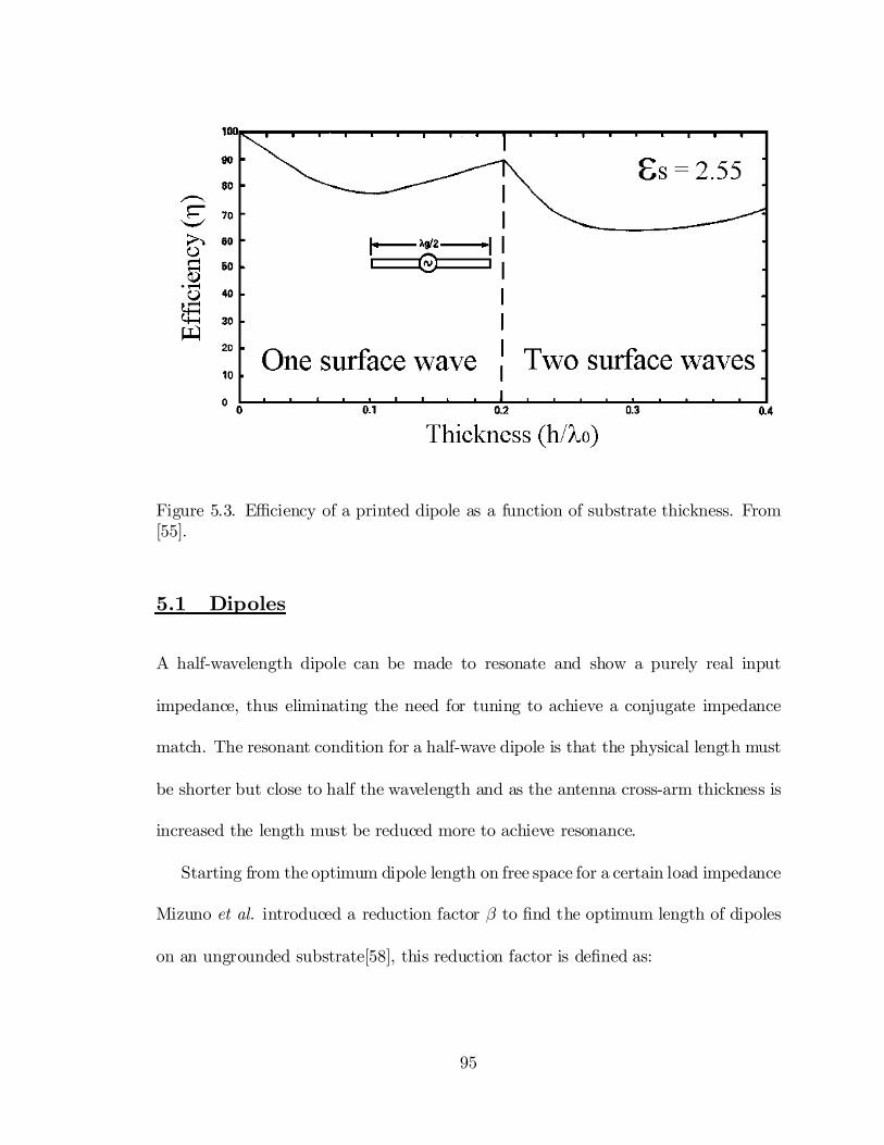
The performance of printed antennas depends on the substrate thickness (h) and
the dielectric constant of the substrate ("s)[57], and there is a certain thickness that
will maximize the performance of a printed antenna for a given dielectric constant.
Figure 5.3 shows the e¢ciency of a half-wave dipole as a function of substrate thickness
h (given in free space wavelengths) for a substrate dielectric constant of "s = 2:55.
The e¢ciency ´ is taken as the ratio of the power radiated into free space to the total
93
Figure 5.2. Printed Antenna on a grounded substrate.
radiated power and multiplied by 100. From Fig. 5.3 we can see that the maximum
e¢ciency is obtained when h ¼ 0:2¸0 which is slightly below the cut-o¤ thickness
of the TE0 substrate guided mode. Figure 5.3 also shows that the e¢ciency is close
to 100% when the substrate thickness is close to zero this is because surface wave
excitation is negligible for very thin substrates.
In this chapter four di¤erent types of microstrip antennas were fabricated on thin
substrates and coupled to microbolometers. These IR antenna-coupled detectors were
measured at 10.6 ¹m and their performance compared. Fabrication was done on 200
nm of SiO2 ("s = 4:84 at 10.6 ¹m) deposited using PECVD, the thickness being much
smaller than the wavelength in the dielectric (h ¼ 0:04¸d, where ¸d = ¸0p"s ), and a 50
nm Cr ground plane. Antennas were made out of 100 nm-thick gold and patterned
using electron beam lithography and lifto¤, and 70 nm of dc-sputtered niobium was
used as the bolometric element.
94
Figure 5.3. E¢ciency of a printed dipole as a function of substrate thickness. From[55].
5.1 Dipoles
A half-wavelength dipole can be made to resonate and show a purely real input
impedance, thus eliminating the need for tuning to achieve a conjugate impedance
match. The resonant condition for a half-wave dipole is that the physical length must
be shorter but close to half the wavelength and as the antenna cross-arm thickness is
increased the length must be reduced more to achieve resonance.
Starting from the optimum dipole length on free space for a certain load impedance
Mizuno et al. introduced a reduction factor ¯ to …nd the optimum length of dipoles
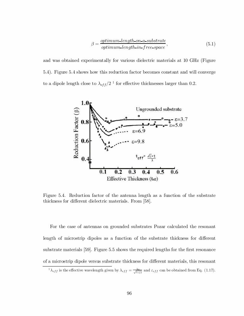
on an ungrounded substrate[58], this reduction factor is de…ned as:
95
¯ =optimum length on a substrateoptimum length in f ree space
; (5.1)
and was obtained experimentally for various dielectric materials at 10 GHz (Figure
5.4). Figure 5.4 shows how this reduction factor becomes constant and will converge
to a dipole length close to ¸eff=2 1 for e¤ective thicknesses larger than 0.2.
Figure 5.4. Reduction factor of the antenna length as a function of the substratethickness for di¤erent dielectric materials. From [58].
For the case of antennas on grounded substrates Pozar calculated the resonant
length of microstrip dipoles as a function of the substrate thickness for di¤erent
substrate materials [59]. Figure 5.5 shows the required lengths for the …rst resonance
of a microstrip dipole versus substrate thickness for di¤erent materials, this resonant1¸eff is the e¤ective wavelength given by ¸eff = ¸0p
"effand "eff can be obtained from Eq. (1.17).
96
length oscilates around a length equal to ¸eff=2. From Figs. (5.4) and (5.5) we can see
that for antennas on grounded substrates the waves propagate at a velocity de…ned
by the e¤ective permittivity (Eq. (1.17)) and this value can be used to calculate the
e¤ective size of printed antennas, in the case of ungrounded antennas this e¤ective
permittivity can be used only when the e¤ective thickness is higher than 0.2, for thin
ungrounded substrates these antennas will behave more like free-space antennas.
Figure 5.5. Resonant length of a half-wave dipole versus substrate thickness. From[55].
Microstrip dipole antennas coupled to Nb microbolometers were fabricated on a
ground plane with a 200 nm SiO2 substrate using electron-beam lithography and
lifto¤ (Fig. 5.6). The grounded substrate is thin enough to reduce losses due to
surface waves and the quasistatic approximation of the e¤ective permittivity can be
97
used for such thickness at 10.6 ¹m (Fig. (1.6)).
Figure 5.6. Dipole-coupled microbolometer.
98
Figure 5.7 shows the response of dipole-coupled microbolometers as a function
of dipole length, we can see how the maximum response is around 3 ¹m which is
close to half the e¤ective wavelength. From Fig. 1.6 we can see how for a 200
nm SiO2 substrate at 10.6 ¹m the e¤ective permittivity is equal to its quasi-static
value ("eff = "s+12 ), since the permittivity of SiO2 is "s = 4:84 at 10.6 ¹m then the
e¤ective permittivity is given by "eff = 2:92 which gives an e¤ective wavelength in
the substrate equal to ¸eff = ¸0p"eff = 10:6¹m1:7 = 6:2 ¹m according to this, the …rst
resonance of the microstrip dipole should be around eff2 =3.1 ¹m which agrees with
the results shown in Figure 5.7.
Figure 5.7. Response of a microstrip dipole as a function of its length.
The polarization dependence of dipole-coupled microbolometers was measured us-
ing a half-wave plate and is shown in Figure 5.8, the maximum response was obtained
99
when the polarization was parallel to the antenna axis. The response as a function of
polarization angle presented a cosine squared dependence which agrees with antenna
theory, the ratio of maximum to the minimum polarization response (polarization
ratio) of these devices was around 4.
Figure 5.8. Polarization Dependence for a dipole-coupled microbolometer.
A two-dimensional scan over the dipole-coupled microbolometer was performed
using an F=1 beam at 10.6 ¹m and is shown in Figure 5.9(a), this …gure represents a
convolution between the detector’s spatial response and the laser beam pro…le. The
collection area of the detector is obtained by deconvolving the two-dimensional scan
100
with the laser beam pro…le. The deconvolution procedure developed in [38] was used
to obtain the spatial response of the detector (Fig. 5.9(b)). The laser beam pro…le
used to deconvolve the two-dimensional scan was modeled as a convolution of a 2-D
Gaussian with a slightly comatic Airy function. A knife-edge scan was …tted to this
model and the resulting beam pro…le was used to perform the deconvolutions.
Figure 5.9. Dipole spatial response (a) convolved with the laser beam, (b) afterdeconvolution. The contours represent 15% increments.
Figure 5.9(b) represents the spatial response of the detector to 10.6 ¹m radiation,
if we approximate the spatial response to a 3D-Gaussian function we can determine
that 85 % of the total volume of the Gaussian is enclosed under the 0:2 z-contour
level. If we de…ne the collection area as the area where 85 % of the collected energy
falls, then from Figure 5.9(b) we can determine that the collection area of these
101
dipole-coupled microbolometers would be approximately 10 ¹m2.
Figure 5.10 shows the radiation pattern of a dipole-coupled niobium microbolome-
ter. This power pattern is related to the e¤ective area of the detector by Eq.(1.21),
where the maximum directivity can be obtained from the power pattern as
Dmax =4¼Umax
Prad; (5.2)
where Umax is the maximum radiation intensity and Prad is the total radiated power.
If we want to calculate the directivity of a printed antenna in the normal direction,
then Umax will be the value of the power pattern at 90o and the total power can be
obtained by calculating the volume under the power pattern P (µ),
Prad = 2¼Z ¼
0P (µ) sin(µ)dµ: (5.3)
Equation (5.3) assumes that the power pattern is omnidirectional (it does not de-
pend on the spherical coordenate Á). For a more accurate calculation of the total
power radiated by an antenna a two-dimensional radiation pattern (µ; Á) needs to be
measured.
By using Eqs. (1.21),(5.2) and (5.3) on the power pattern shown in Fig. 5.10 we
…nd that the directivity in the normal direction for this dipole antenna is 1.7 and
the calculated e¤ective area is around 52 ¹m2, the di¤erence between measured and
calculated e¤ective areas is due to re‡ection and dielectric conduction losses, therefore
102
the radiation e¢ciency of this antenna is the ratio of measured and calculated e¤ective
areas, which is around 20 %.
Figure 5.10. Radiation pattern of a dipole-coupled microbolometer.
103
These dipole-coupled niobium microbolometers presented an average dc-resistance
of 80§ 5 , were illuminated using a laser beam at 10:6 ¹m and F=8 optics, with a
power at the focal plane of 43:4 mW and an irradiance of 117 W=cm2. The measured
response to the incident infrared radiation was around 11§ 2 ¹V for the polarization
parallel to the dipole antenna, the noise was around 29 nVpHz
, which gives a signal-
to-noise ratio (SNR) of » 380, a Responsivity of 0:8 V=W and a D¤ of 8:6 £ 103
cmpHz
W .
5.2 Bowties
If an antenna is made using perfect conductors and dielectrics and its dimensions
change, the characteristics of that antenna (impedance, polarization, radiation pat-
tern, etc) will remain the same as long as the wavelength of operation is changed in
the same amount. Therefore, if the shape of an antenna is determined only by angles,
the performance of that antenna would be independent of frequency since it would
be invariant to a change of scale [52], bowties, spirals and log-periodic antennas are
examples of frequency independent antennas.
The main advantages of bowtie antennas are simple design and broad-band im-
pedance. A bowtie antenna is made from a bi-triangular sheet of metal with the
feed at its vertex. This type of antenna, which is only de…ned by the bow angle µ,
would be frequency independent if it extended to in…nity on both sides. To fabricate
a practical bow-tie antenna we must have a …nite gap between the feed points and
104
a …nite size which would result in limited bandwidth, however typically the antenna
can be terminated with a bow-arm length of 2¸eff without a signi…cant e¤ect on the
pattern or the impedance [11].
The radiation of a bowtie antenna is linearly polarized and has a bidirectional
pattern with broad main beams perpendicular to the plane of the antenna. The
impedance can be calculated accurately from transmission line theory[40] and is given
by:
Z =
s2¹0
"eff + "0¢ K(k)K0(k)
; (5.4)
where
K(k) =Z 1
0
dxp(1 ¡ x2)(1¡ k2x2)
;K 0(k) = K(k0); (5.5)
and
k0 =p1¡ k2: (5.6)
K and K0 are elliptic integrals of the …rst kind, k = tan2(45o ¡ µ=4) and µ is
the bow angle. Figure 5.11 shows the impedance of a bowtie antenna on a silicon
substrate as a function of the ‡are angle, this impedance is purely real for any bow
angle, this behavior has been demonstrated experimentally in [40].
Figure 5.12 shows an electron micrograph of a planar bowtie antenna similar to
the one used in this study. The antenna is 4 ¹m long and has a bow angle of around
105
Figure 5.11. Impedance of a Bowtie antenna on a Silicon substrate as a function ofthe ‡are angle.
60 degrees which would yield an impedance close to 75 ; intended to match the
impedance of the sensing Nb patch.
Figure 5.13 shows the polarization response of a bowtie-coupled microbolome-
ter, this response also follows a cosine squared dependence, characteristic of linearly
polarized antennas and it presented a polarization ratio close to 17.
Figures 5.14(a) and 5.14(b) show a two dimensional scan over a bowtie-coupled
microbolometer and the spatial response of the same device to 10:6 ¹m radiation
after deconvolution. From Figure 5.14(b) we can see that the e¤ective collection area
of the bowtie-coupled microbolometer is close to » 14 ¹m2. Figure 5.15 shows the
radiation pattern of a bowtie-coupled niobium microbolometer, the directivity in the
normal direction for this power pattern is 1.2 and the calculated e¤ective area is
106
Figure 5.12. Bowtie-coupled microbolometer.
107
Figure 5.13. Polarization Dependence for a bowtie-coupled microbolometer.
108
around 37.5 ¹m2 the radiation e¢ciency of this antenna, comparing the calculated
and the measured e¤ective area, is around 37 %.
Figure 5.14. Bowtie spatial response (a) convolved with the laser beam, (b) afterdeconvolution. The contours represent 15% increments.
These bowtie-coupled niobium microbolometers presented an average dc-resistance
of 90§ 5 , were illuminated using a laser beam at 10:6 ¹m and F=8 optics, with a
power at the focal plane of 43:4 mW and an irradiance of 117 W=cm2. The measured
response to the incident infrared radiation was around 14§ 1 ¹V for the polarization
parallel to the bowtie antenna, the noise was around 29 nVpHz
, which gives a signal-
to-noise ratio (SNR) of » 482, a Responsivity of 0:72 V=W and a D¤ of 9:3 £ 103
cmpHz
W .
109
Figure 5.15. Radiation Pattern of a bowtie-coupled niobium microbolometer.
5.3 Square Spirals
The equiangular spiral is a geometrical con…guration that can be described just by
angles, therefore it ful…lls the requirement for shapes that can be used to design fre-
quency independent antennas. The lower limit of their frequency bandwidth depends
on the outer circumference of the spiral and the upper frequency limit depends on
the con…guration near the feed point. Spiral antennas are circularly polarized with
a sense that depends on the winding sense of the spirals. A square spiral antenna is
regarded as a counterpart of a round spiral antenna with the advantage that it o¤ers
a size reduction of 22 % (based on the increase of perimeter from ¼D to 4D)[60].
The radiating characterstics of this antenna can be explained by modelling it as a
two-wire transmission line. A current wave traveling along the arms of the antenna
radiates energy which decreases the amplitude of the current along the conducting
antenna arms, and beyond a certain point the presence or absence of the conductor
110
makes little di¤erence. The point of negligible current occurs about one wavelength
from the feed point[61], therefore when the wavelength is shorter than the arm length,
the performance is practically frequency independent. If the antenna arms become
shorter than the wavelength the polarization becomes elliptical where its axial ratio
increases by decreasing the arm length until the polarization becomes linear and the
spiral becomes a dipole.
Figure 5.16. Geometry of a two-wire square spiral antenna.
Figure 5.16 shows the geometry of a two-wire square spiral antenna, the antenna
arms A and B are composed of linear …laments wound in the X-Y plane where the
length of the nth-…lament is given by:
Ln =
8>><>>:
a
2a(n¡ 1)
for
for
n = 1
n = 2; 3; :::: (5.7)
111
A planar spiral antenna with arms 17 ¹m long, 200 nm wide and 100 nm thick
made out of gold with a Nb microbolometer in the feed point is shown in Figure 5.17.
This antenna was fabricated on a 200 nm SiO2 substrate and a Cr ground plane.
Figure 5.17. Spiral-coupled microbolometer.
Figure 5.18 shows the polarization response of a square–spiral-coupled microbolome-
ter to linearly polarized radiation at 10.6 ¹m, spiral antennas have circular polariza-
tion for wavelengths smaller than the arm length, this spiral-antenna presented a
linear-polarization ratio close to 1.5 which indicates that the polarization of the an-
112
tenna is actually elliptical, this ellipticity might be due to contributions to the total
response of the bias leads acting as long dipoles which are linearly polarized. The
orientation of the principal axis of the elliptical polarization corresponds to the angle
where the maximum response is found.
Figure 5.18. Polarization dependence of a Square-spiral-coupled microbolometer.
Figures 5.19(a) and 5.19(b) show the two-dimensional scan of a spiral-coupled
microbolometer and its deconvolution with the laser beam to …nd the e¤ective col-
lection area of the detector. From Figure 5.19(b) we can see that » 85 % of the
maximum infrared radiation is collected on an area of » 12:5 ¹m2. Figure 5.20 shows
113
the radiation pattern of a spiral-coupled niobium microbolometer, the directivity in
the normal direction for this power pattern is 1.6 and the calculated e¤ective area is
around 49 ¹m2 which gives a radiation e¢ciency close to 25 %.
Figure 5.19. Spiral spatial response (a) convolved with the laser beam, (b) afterdeconvolution. The contours represent 15% increments.
114
Figure 5.20. Radiation Pattern of a spiral-coupled niobium microbolometer.
The spiral-coupled niobium microbolometers were measured using a 10:6 ¹m CO2
laser and F=1 optics, the power at the focal plane was 8:7 mW with an irradiance of
1506 W=cm2, the detectors presented an average dc-resistance of 1:4§ 0:2 k. The
measured response to the incident infrared radiation was around 1:8 § 0:2 mV, the
noise measured was 160 nVpHz
, which gives a signal-to-noise ratio (SNR) of » 11; 250,
a Responsivity of 9.5 V=W and a D¤ of 2:1£ 104 cmpHz
W .
5.4 Log-Periodic
If a special kind of repetitiveness in the physical structure of an antenna is introduced
a repetitive behavior of the electrical characteristics will be obtained. In log-periodic
antennas the geometry is chosen so that the electrical properties repeat themselves
with the logarithm of the wavelength. Frequency independence can be obtained when
variation of the electrical characteristics over one period is small.
115
The log-periodic toothed planar antenna is similar to the bowtie antenna except
for the teeth. The teeth act to disturb the currents which would ‡ow if the antenna
were of bowtie-type construction. The radiation is linearly polarized parallel to the
teeth edges, this is perpendicular to what it would be if there were no teeth, in which
case the antenna would be a bowtie. This shows that the component of current that
‡ows in the direction of the teeth dominates the radial component[52].
Figure 5.21 shows a log-periodic toothed planar antenna, if ¯1 + ¯2 = 90o the
antenna becomes self-complementary in which case it will have a constant impedance
of 189 at all frequencies[52]. Also for a log-periodic toothed planar antenna the
ratio of edge distances is constant and is given by the following scale factor:
¿ =Rn+1
Rn; (5.8)
the paramenter ¿ gives the period of the structure, therefore a periodic pattern and
impedance behavior with the same period would be expected.
Figure 5.22 shows an electron micrograph of a planar log-periodic antenna with
a scale factor of ¿ ¼ 2 coupled to a niobium microbolometer, this antennas were
fabricated on 200 nm of SiO2 and a chrome ground plane, the antenna and bias lines
are made out of 100 nm of evaporated gold and the microbolometer is made out of
a 70 nm …lm of sputtered niobium, the microbolometer is placed at the feed point
of the antenna. The antenna is resonant when the length of any of the arcs An (as
shown in Fig. 5.21) is equal to eff2 ; the arc length can be calculated as:
116
Figure 5.21. Log-periodic toothed planar antenna.
117
An =³¼2
´µRn + rn
2
¶; (5.9)
for ¯1+ ¯2 = 90o: The corresponding resonant frequencies are:
fn =2c
¼ (Rn + rn)p"eff
: (5.10)
The log-periodic antenna shown in Fig. 5.22 was designed to have a frequency cover-
age of 18 - 70 THz which corresponds to a wavelength coverage of 4-16 ¹m:
Figure 5.22. Log-periodic antenna coupled to a microbolometer.
118
Figure 5.23 shows the polarization response of a log–periodic-coupled microbolome-
ter, this response also follows a cosine squared dependence characteristic of linearly
polarized antennas, the maximum response is obtained for a polarization parallel to
the dc leads which is perpendicular to the polarization of a bowtie and a dipole, the
polarization ratio close to 1.4. This low polarization ratio is due to the cross-polarized
response given by the bowtie-like part of the log-periodic structure which competes
with its co-polarized response, this vector addition of polarizations does not a¤ect
the magnitude of the co-polarized response.
Figure 5.23. Polarization dependence for a log-periodic antenna-coupled detector.
119
Figures 5.24(a) and 5.24(b) show the two-dimensional scan of a log–periodic-
coupled microbolometer and its deconvolution with the laser beam to …nd the ef-
fective collection area of the detector. From Figure 5.24(b) we can see that » 85%
of the maximum infrared radiation is collected on an area of » 21 ¹m2. Figure 5.25
shows the radiation pattern of a log–periodic-coupled niobium microbolometer, the
directivity in the normal direction for this power pattern is 1.5 and the calculated
e¤ective area is around 45.6 ¹m2 which gives a radiation e¢ciency close to 46 %.
Figure 5.24. Spatial response for a log-periodic antenna (a) convolved with the laserbeam, (b) after deconvolution. The contours represent 15% increments.
120
Figure 5.25. Radiation pattern of a log–periodic-coupled niobium microbolometer.
The log–periodic-coupled niobium microbolometers were measured using a 10:6
¹m CO2 laser and F=1 optics, the power at the focal plane was 8:7 mW with an
irradiance of 1506 W=cm2, the detectors presented an average dc-resistance of 400§50
. The measured response to the incident infrared radiation was around 0:9 § 0:2
mV, the noise measured was 80 nVpHz , which gives a signal-to-noise ratio (SNR) of
» 11250, a Responsivity of 2:84 V=W and a D¤ of 1:6£ 104 cmpHz
W .
121
CHAPTER 6
ANTENNA-COUPLED IR PIXELS
Antenna-coupled microbolometers can have collection areas as small as 10 ¹m2. De-
tectors this small are unsuitable for imaging applications where a typical pixel area
ranges from 20£ 20 ¹m2 to 50 £ 50 ¹m2 [62]. In this chapter two di¤erent types of
detectors that can cover a typical pixel area are fabricated and their characteristics
measured. The …rst type of IR pixel is a two-dimensional array of antenna-coupled
microbolometers that will increase the collection area of a single element to cover
a whole pixel area, the second IR pixel is a Fresnel Zone Plate (FZP) coupled mi-
crobolometer. A FZP is used to collect the radiation that falls on a pixel area and will
focus it on a single element microbolometer. These FZPs are fabricated using optical
lithography and lifto¤ and were aligned to the microbolometers by using a back-side
aligner. Responsivity and radiation characteristics of these two types of pixels were
measured and compared to single element microbolometers.
122
6.1 2D Array of Antenna-Coupled Microbolometers.
A two-dimensional array of antenna-coupled microbolometers that will increase the
area of the detector without sacri…cing the response and time constant characteristic
of microbolometers is proposed, fabricated and its performance compared to single
element antenna-coupled microbolometers.
6.1.1 Antenna Array Theory
An array of antennas is an assembly of radiating elements such that the radiation from
the elements “adds up” to give a maximum …eld intensity in a particular direction or
directions and cancels or very nearly cancels in others. In addition to placing elements
along a line (to form a linear array), individual radiators can be positioned along a
rectangular grid to form a rectangular or planar array (Figure 6.1). Planar arrays
provide additional variables which can be used to control and shape the pattern of the
array. Planar arrays are more versatile and can provide more symmetrical patterns
with lower sidelobes. In addition they can be used to scan the main beam of the
antenna toward any point in space by controlling inter-element phase.
123
Figure 6.1. Rectangular array of antennas. From [1].
The total …eld of the array is equal to the …eld of a single element positioned at
the origin multiplied by a factor which is widely referred to as the “Array Factor”
(AF) [1]:
AFn(µ; Á) =
8<:
1M
sin¡M
2 Ãx¢
sin³Ãx2
´
9=;
8<:
1N
sin¡N2 Ãy
¢
sin³Ãy2
´
9=; ; (6.1)
where Ãx = kdx sin µ cos Á + ¯x, and Ãy = kdy sin µ sinÁ + ¯y, M and N are the
number of antennas in the x and y directions respectively, dx and dy are the distance
between elements in the x and y directions and ¯x and ¯y are the progressive phase
di¤erences between elements in the x and y directions.
When the spacing between the elements is equal or greater than ¸=2, multiple
124
maxima of equal magnitude can be formed. The principal maximum is referred to as
the “major lobe” and the remaining as the “grating lobes”. To avoid grating lobes
in the xz and yz planes, the spacing between the elements in the x and y directions,
respectively, must be less than ¸=2 (dx < ¸=2 and dy < ¸=2). From Eq. 6.1 we can
also see that the maximum value of the array factor is obtained when the distance
between the elements is ¸=2.
In the case of antenna-coupled microbolometers, currents at THz frequencies are
induced in the antenna elements by infrared radiation and are dissipated in the mi-
crobolometer which, being a power detector, converts that energy into a dc signal.
Therefore any phase information is lost, however some of the energy ‡ows out of
the antenna through the substrate and can couple to adjacent antennas providing an
“array e¤ect”.
6.1.2 Element Spacing
In order to optimize the response of a rectangular array of antenna-coupled detectors
the characteristics of a single element and the spacing between the elements that
maximizes the response to normally incident infrared radiation has to be obtained.
According to antenna-array theory optimum radiation characteristics in the direc-
tion perpendicular to the planar array are obtained with a spacing of ¸=2, however
Fumeaux et al. [63] also discovered that at infrared frequencies the surface impedance
of metals play an important role in the behavior of THz currents shortening the wave-
125
length of the propagating current and therefore shifting the resonant frequency of
dipole antennas. The fact that these e¤ects are not taken into account in equations
that appear in antenna theory books makes it necessary to …nd the optimum spacing
and length of elements in an infrared antenna array experimentally.
Rana and Alexopoulos calculated the mutual coupling between two broadside reso-
nant microstrip dipoles on thin substrates[64], Figure 6.2 shows the mutual impedance
between two parallel broadside dipoles as a function of their separation, there we can
see that the resonances (where the mutual impedance is purely real) are located at a
distance close to 0:3; 0:85 and 1:3 e¤ective wavelengths. The e¤ective wavelength is
given by ¸eff = 0p"eff ; where "eff ="SiO2+1
2 :
A distance study of dipole-coupled microbolometers was performed using gold for
the antenna elements and niobium for the bolometric material on a 200 nm layer
of SiO2 ("SiO2 = 4:84 at 10.6 ¹m) as substrate and a 50 nm chrome ground plane.
Figure 6.3 shows the response of these two broadside dipoles to 10.6 ¹m radiation for
di¤erent spacings. There is a peak in the response at 2:4 ¹m which is 0.38 e¤ective
wavelengths, close to the …rst resonance of the mutual coupling of two broadside
dipoles found in [64]. Interestingly enough 2:4 ¹m is a half wavelength in the dielectric,
as if the antennas were not at an air-dielectric interface ( ¸02p"SiO2
= 10:6¹m2p4:84
= 2:4 ¹m),
this indicates that coupling between printed dipoles at an air-dielectric interface may
be caused by surface-waves and there might be phase addition at the surface-wave
level that increases the response at half the wavelength in the substrate, inducing an
126
Figure 6.2. Calculated mutual impedance between two broadside microstrip dipoles.From [64].
127
antenna-array e¤ect.
Figure 6.3. Coupling of dipoles as a function of distance.
6.1.3 Response and Noise analysis
A series array of microbolometers was chosen to match the impedance of commercial
readout integrated circuits (ROIC’s), and to cover the typical pixel area used in
commercial infrared imaging systems. The Johnson noise of a microbolometer is
given by
128
Vj =p
4KTR¢f ; (6.2)
where K is the Boltzmann constant, T is the Temperature in K, R is the resistance
of the microbolometer and ¢f is the bandwidth of the measurement. By making an
N £N array of microbolometers the total resistance of the detector will increase by
a factor of N2: From Eq. (6.2), we can see that this will result in a N£ increase
in Johnson noise. However from Eq. (1.13) we can see that the response is directly
proportional to the resistance of the microbolometer, therefore a resistance increase
of a factor of N2 will increase the response in the same amount giving an anticipated
increase of N£ in signal-to-noise ratio of a serial array compared to a single element
microbolometer.
6.1.4 Experimental Results
Four di¤erent types of serial arrays of microbolometers that can cover the area of a
picture element in an infrared imaging system were fabricated and tested. Dipoles
and bowties in two di¤erent con…gurations were used, those parallel to the bias cur-
rent (Figs. 6.5 and 6.6) will be called parallel-dipole and bowtie arrays and those
with elements perpendicular to the bias current (Figs. 6.7 and 6.8) will be called
perpendicular-dipole and bowtie arrays respectively. All these devices were fabri-
cated on a 200 nm SiO2 substrate and a chrome ground plane, the antenna elements
are made out of gold and niobium is used as the bolometric material. These ar-
129
Figure 6.4. Series array of bolometers.
rays cover an area of 50 £ 50 ¹m2 and the spacing between elements is 5 ¹m, this
spacing represents 0.8 e¤ective wavelengths which is close to the second surface-wave
resonance (Fig. 6.2).
Knowing that antenna-coupled microbolometers respond to visible frequencies
[65], a two-dimensional scan was performed using a HeNe laser in the visible, these
type of measurements are an e¤ective way of characterizing the homogeneity of the
detectors and the e¤ectiveness of the fabrication process[43]. The beam of the HeNe
laser was focused at the center of the array by moving the detector along the three
axes and maximizing its response. The two-dimensional scan was performed by keep-
ing the z axis …xed, moving the device in the x and y directions and recording the
response of the device in each position. Figure 6.9 shows a two-dimensional scan of
130
Figure 6.5. Parallel Dipole Array.
Figure 6.6. Parallel Bowtie Array.
131
Figure 6.7. Perpendicular Dipole Array.
Figure 6.8. Perpendicular Bowtie Array.
132
a 5 £ 5 array of microbolometers. From the scan the individual response of each
element of the array can be observed and determine the uniformity of the single ele-
ment microbolometers that form the array, this type of measurement can be used as
a diagnostic tool to determine the quality of the array and detect possible defects in
the fabrication process.
Figure 6.9. Two-dimensional scan in the visible for a 5£ 5 array of microbolometers.
133
A two-dimensional scan in the infrared was also performed on a single element,
5 £ 5 array and 10 £ 10 array of microbolometers to determine the detection area
covered by each device. The two-dimensional scans were taken following the same
procedure used for the scan in the visible, but using a CO2 laser at 10:6 ¹m and F=1
optics. The F=1 optics presented an almost di¤raction-limited focal spot of 12 ¹m in
radius. Figures 6.10(a),(b) and (c) show 80£ 80 ¹m2 scans on a single element, 5£ 5
array and 10£ 10 array respectively. The scan on the single element (Figure 6.10(a))
showed only the beam pro…le, which indicates that the single element microbolometer
can be considered as nearly a point receiver at infrared frequencies. Figures 6.10(b)
and (c) show how the detection area increases by going from a single element to a
two-dimensional array of microbolometers. A uniform detection area of approximately
25£ 25 ¹m2 and 50£ 50 ¹m2 are shown in Figures 6.10(b) and (c) respectively, these
areas correspond to the physical size of the receivers. From the results shown in
Figure 6.10 we can see that two-dimensional arrays of microbolometers make uniform
area detectors and can be used as pixel elements in infrared imaging systems.
Figure 6.11 shows a comparison of the response for the di¤erent types of two
dimensional arrays of microbolometers to infrared radiation, the parallel arrays pre-
sented a higher response than the perpendicular array of detectors, and the bowties
had a higher response than the dipoles. All the measurements were made with a
CO2 laser at 10:6 ¹m and F=8 optics at the optimum polarization for each type of
detectors, the optimum polarization for all the detectors was the one parallel to the
134
Figure 6.10. Two-dimensional scan in the infrared (CO2 laser at 10:6¹m), for (a)Single Element, (b) 5 £ 5 array and (c) 10 £ 10 array of microbolometers. Thedimensions are given in microns.
antenna arms, therefore the optimum polarization for the parallel arrays is 90 degrees
rotated with respect to the optimum polarization of the perpendicular arrays.
In order to test the performance of a single element compared to an array of
detectors, a single element square-spiral antenna (Fig. 6.12(a)) and a 9 £ 9 array
of square-spirals (Fig. 6.12(b)) were fabricated and tested. Single element detectors
had a dc resistance around 80 and were biased at 100 mV (bias current of 1.25
mA) while the arrays had a resistance around 1.3 k and were biased at 300 mV
(bias current of 230 ¹A). Noise and response measurements at 10.6 ¹m were made,
single element square spiral antennas gave a response of 10§1 ¹V and a noise …gure
of 3.5§0.3 nVpHz
. The 2D-Array of square spiral antennas presented a response of
25§3 ¹V with a noise …gure of 5.5§0.8 nVpHz; however these devices were biased at a
current 5:4£ lower than the single elements, if we normalize to the bias current of
the single element detectors the response of the arrays would be around 135 ¹V. The
135
Figure 6.11. Voltage response of di¤erent 2D-Arrays of antenna-coupled microbolome-ters to infrared radiation.
136
SNR for a single element detector was » 2860, while for the two-dimensional array
was » 4550 (normalized to » 24500), however D¤ which is a …gure of merit that
permits comparison of detectors of the same type but having di¤erent areas gave a
value of 3:2 £ 104 cmpHz
W for the single element detector and 5 £ 103 cmpHz
W for the
arrays (normalized to 2:7£ 104 cmpHz
W ), therefore going from single element detectors
to two-dimensional arrays will increase the signal-to-noise ratio but not D¤, which is
the main …gure of merit for infrared detectors.
According to Eq. (6.2) the Johnson noise for the single element detectors tested
is 1.1 nVpHz
and for the detector array is 4.6 nVpHz; from the noise measurements we
can see how 1=f noise is dominant in single element detectors and by going to an
array the 1=f noise contributions of every single element does not add in quadrature
like Johnson noise does, this seems to indicate that the noise sources are correlated
to each other through the fabrication process. The increase in response between
single element detectors and arrays normalized to the bias current is around 13:5£
which is close to the ratio of dc resistances (16:5£), this 20% di¤erence is due to the
contribution of the bias lines to the dc resistance but not to the bolometric response.
It is also worth noting that the signal to noise ratio had an increase of around 8:6£
which is close to the 9£ theoretical increase (N£ for an N £N array).
137
6.2 Fresnel Zone Plate Lens
A Fresnel Zone Plate Lens (FZPL) was fabricated to collect infrared energy and focus
it on a single antenna-coupled microbolometer, keeping the noise level low and still
having a large collection area. The performance of these devices is compared to that
of a two-dimensional array of detectors. The FZP lenses were patterned using optical
lithography and aligned to single element square-spiral-coupled microbolometer on
the backside of the wafer using an EV620 backside aligner. The FZP lenses were
made out of 100 nm of e-beam evaporated Au over a 5 nm layer of Cr. The FZP
lens was designed to work at a wavelength of 10.6 ¹m with a focal length of 380 ¹m,
close to the substrate thickness so that the antenna-coupled detector would be at its
focus(Figure 6.13). The main function of the zone plate is to increase the gain of the
spiral antenna and also reduce the energy loss due to guided waves in the substrate
by altering the boundary conditions of the dielectric slab waveguide[66].
Fresnel zone plates work by concentrating energy of an incident plane wave by
blocking the portions that would add destructively at the focal point. This e¤ect can
be explained using the Huygens-Fresnel principle were the wavefront is replaced by
point sources in the open region of the zone plate. The geometry of the zone plate is
such that these point sources emit waves that arrive at the focal point with a relative
phase between 0 and ¼. In contrast, if point sources are placed in the adjacent blocked
regions of the zone plate, their waves would arrive at the focal point with a relative
phase between ¼ and 2¼. Since these waves would add destructively to the …eld at
138
Figure 6.12. Square Spirals. (a) Single Element, (b) Two dimensional array.
Figure 6.13. Fresnel Zone Plate Lens in the transmissive con…guration coupled to amicrobolometer.
139
the focal point they are blocked by an opaque zone.
The determination of the open and opaque regions is cylindrically symmetric about
the zone-plate/focal-point axis. This cylindrical symmetry gives the zone plate its
characteristic light and dark rings. The boundary between the open and opaque rings
can be determined by geometry, by calculating the phase di¤erence that will result
from light traveling di¤erent distances. First the focal length f of the zone plate is
chosen, and then the radii of the zone plate rings is determined. The equation for the
nth radii rn is given by [67]
rn =
snf¸ +
µn¸2
¶2
: (6.3)
This zone plate is called a transmission zone plate since it concentrates the wave as
it passes through the open rings (Fig. 6.14(a)).
A variation of the zone plate is made by placing a re‡ecting surface in the opaque
regions. In this case another focal point is formed on the incident-wave side of the zone
plate (Fig. 6.14(b)), this variation is called a re‡ection zone plate since it concentrates
the wave by re‡ecting it from the opaque rings.
Two di¤erent types of Fresnel Zone Plate Lenses were fabricated, the traditional
ones which consist of concentric rings (Figure 6.15) and an approximation to these
made using concentric squares (Figure 6.16). Eight circular and …ve square FZPs
were fabricated, these lenses vary in the number of zones each one has, circular FZPs
go from 1 to 8 opaque zones while square FZPs go from 1 to 5 opaque zones. Figure
140
Figure 6.14. Illustration of (a) transmission zone plate, (b) re‡ection zone plate.
6.17 shows the results obtained by using circular FZP lenses in the transmissive
and re‡ective con…guration (the re‡ective con…guration would be with the radiation
coming through the detector …rst and then re‡ecting o¤ the FZP), these results are
normalized to the response obtained with a detector without an FZP, in this case the
transmissive circular FZP gave a higher response than the re‡ective one, the response
does not increase more with lenses above the sixth opaque zone because the lenses
become bigger than the F=8 spot used to test them.
By increasing the number of Fresnel zones the response of the detector increases.
However the collection area of the detector, which is the area covered by the largest
zone plate, also increases. Figure 6.18 shows the gain of a circular FZP in the trans-
missive mode as a function of the number of opaque Fresnel zones, next to each of
141
Figure 6.15. Circular FZPs.
142
Figure 6.16. Square FZPs.
143
Figure 6.17. Results for Circular FZPs.
the measured points is the ratio of the calculated D¤ for the FZP-coupled detector
and a detector without an FZP, from these results we can see that we get an increase
in D¤ after the …fth opaque zone which is around 200 ¹m in diameter. Figure 6.18
also shows the expected gain increase for a transmissive circular zone plate, which is
proportional to N2 where N is the number of zones. From these results we can see
that a 50£ 50 ¹m2 FZP-coupled infrared pixel gives a low D¤, making them not the
best option for infrared imaging systems.
Figure 6.19 shows the results obtained by using square FZP lenses in the trans-
missive and re‡ective con…guration, these results are also normalized to the response
obtained with a detector without an FZP, in this case the re‡ective FZP gave a
higher response than the transmissive one, since these square FZPs are aproxima-
144
Figure 6.18. Gain of a circular FZP in the transmissive mode and normalized D¤ asa function of Fresnel zones.
145
tions to the circular ones the higher response in the re‡ective case could be due to
the fact that the gold structure is more e¢cient as a simple metal re‡ector than as
a di¤raction-based concentrator. The square FZPs are designed by making squares
that have the same area as its circular counterparts, this approximation works better
for some square dimensions than for others, that is why the gain oscilates and does
not increase monotonically.
Figure 6.19. Results for Square FZP’s.
A comparison was made between a 50 £ 50 ¹m2 2D-array of square spirals and
a single antenna with a circular FZP with a diameter of 223 ¹m and consisting of 6
opaque fresnel zones. The 2D-Array of square spiral antennas presented a response of
25§3 ¹Vwith a noise …gure of 5.5§0.8 nVpHz
, while the FZP-coupled detectors presented
146
a response of 1.1§0.1 mV and the noise …gure was 3.5§0.2 nVpHz
, which translates into
an SNR of » 455 and D¤ of 5£103 cmpHz
W for the 2D array and an SNR of » 33£ 103
and D¤ of 9:5 £ 104 cmpHz
W for the FZP-coupled detector.
The angular response of these two detectors was also measured, Fig. 6.20(a) shows
the radiation pattern for a 2D array of square spirals and Fig. 6.20(b) shows the
radiation pattern for an FZP-coupled square spiral microbolometer. The directivity
of the 2D array is 1.6 with a 50 £ 50 ¹m2 area and the FZP has a directivity of 4.1
for an area of 31,415 ¹m2 (100 ¹m-radius zone). With the FZP-coupled detector we
gain 2:5£ in directivity with an area increase of 12:5£; which indicates that the 2D
array is a more e¢cient area receiver than the FZP-coupled detector.