11.25Gbps SFP Optical Transceiver, 20km Reach Features Dual data-rate of 1.25Gbps/1.063Gbps operation 1310nm FP laser and PIN photodetector for 20km transmission Compliant with SFP MSA and SFF-8472 with duplex LC receptacle Digital Diagnostic Monitoring: Internal Calibration or External Calibration Compatible with SONET OC-24-LR-1 Compatible with RoHS +3.3V single power supply Operating case temperature: Standard : 0 to +70°C Industrial : -40 to +85°C Appl ic ati ons Gigabit Ethernet Fiber Channel Switch to Switch interface Switched backplane applications Router/Server interface Other optical transmission systems Description The SFP transceivers are high performance, cost effective modules supporting dual data-rate of 1.25Gbps/1.0625Gbps and 20km transmission distance with SMF. The transceiver consists of three sections: a FP laser transmitter, a PIN photodiode integrated with a trans-impedance preamplifier (TIA) and MCU control unit. All modules satisfy class I laser safety requirements. The transceivers are compatible with SFP Multi-Source Agreement (MSA) and SFF-8472. For further information, please refer to SFP MSA.
Transcript
8/10/2019 AOP-324-R20_D
http://slidepdf.com/reader/full/aop-324-r20d 1/9
1
1.25Gbps SFP Optical Transceiver, 20kmReach
Features
Dual data-rate of 1.25Gbps/1.063Gbps operation
1310nm FP laser and PIN photodetector for 20km transmission
Compliant with SFP MSA and SFF-8472 with duplex LC
receptacle
Digital Diagnostic Monitoring:
Internal Calibration or External Calibration
Compatible with SONET OC-24-LR-1
Compatible with RoHS
+3.3V single power supply
Operating case temperature:
Standard : 0 to +70°C
Industrial : -40 to +85°C
Appl ications
Gigabit Ethernet
Fiber Channel
Switch to Switch interface
Switched backplane applications
Router/Server interface
Other optical transmission systems
Description
The SFP transceivers are high performance, cost effective modules supporting dual data-rate of1.25Gbps/1.0625Gbps and 20km transmission distance with SMF.
The transceiver consists of three sections: a FP laser transmitter, a PIN photodiode integrated with atrans-impedance preamplifier (TIA) and MCU control unit. All modules satisfy class I laser safetyrequirements.
The transceivers are compatible with SFP Multi-Source Agreement (MSA) and SFF-8472. For furtherinformation, please refer to SFP MSA.
8/10/2019 AOP-324-R20_D
http://slidepdf.com/reader/full/aop-324-r20d 2/9
2
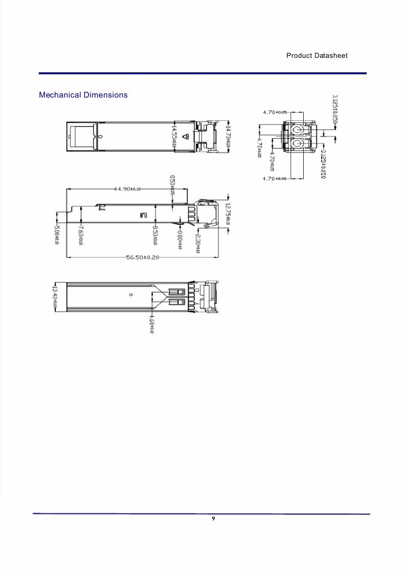
Product Datasheet
Absolute Maximum Ratings
Table 1 - Absolute Maximum Ratings
Parameter Symbol Min Max Unit
Supply Voltage Vcc -0.5 4.5 V
Storage Temperature Ts -40 +85 °C
Operating Humidity - 5 85 %
Recommended Operating Conditions
Table 2 - Recommended Operating Condi tions
Parameter Symbol Min Typical Max Unit
Standard 0 +70 °COperating Case Temperature
Industrial
Tc
-40 +85 °C
Power Supply Voltage Vcc 3.13 3.3 3.47 V
Power Supply Current Icc 300 mA
Data Rate 1.25 Gbps
Optical and Electrical Characteristics
(FP and PIN, 1310nm, 10km Reach) Table 3 - Optical
and Electrical Characteristics
Vcc
Temp
TD+/-
TxFault
TxDis
LOS
RD+/-
SCLSDA
LD Driver LD
PIN+TIAPost Amp
MCUEEPROM ADC/DAC
8/10/2019 AOP-324-R20_D
http://slidepdf.com/reader/full/aop-324-r20d 3/9
3
Product Datasheet
Parameter Symbol Min Typical Max Unit Notes Transmitter
Centre Wavelength λc 1260 1310 1360 nm
Spectral Width (RMS) ∆λ 4 nm
Average Output Power Pout -9 0 dBm 1
Extinction Ratio ER 9 dB
Optical Rise/Fall Time (20%~80%) tr/tf 0.26 ns
Data Input Swing Differential VIN 400 1800 mV 2
Input Differential Impedance ZIN 90 100 110 Ω
Disable 2.0 Vcc VTX Disable
Enable 0 0.8 V
Fault 2.0 Vcc VTX Fault
Normal 0 0.8 V
Receiver
Centre Wavelength λc 1260 1360 nm
Receiver Sensitivity -23 dBm 3
Receiver Overload -3 dBm 3
LOS De-Assert LOSD -24 dBm
LOS Assert LOS A -36 dBm
LOS Hysteresis 1 4 dB
Data Output Swing Differential Vout 370 1800 mV 4
High 2.0 Vcc VLOS
Low 0.8 V
Notes:
1. The optical power is launched into SMF.2. PECL input, internally AC-coupled and terminated.3. Measured with a PRBS 2
7-1 test pattern @1250Mbps, BER ≤1×10
-12.
4. Internally AC-coupled.
Timing and Electrical
Table 4 - Timing and Electrical
Parameter Symbol Min Typical Max Unit
Tx Disable Negate Time t_on 1 ms
8/10/2019 AOP-324-R20_D
http://slidepdf.com/reader/full/aop-324-r20d 4/9
4
Product Datasheet
Tx Disable Assert Time t_off 10 µs
Time To Initialize, including Reset of Tx Fault t_init 300 ms
Tx Fault Assert Time t_fault 100 µs
Tx Disable To Reset t_reset 10 µs
LOS Assert Time t_loss_on 100 µs
LOS De-assert Time t_loss_off 100 µs
Serial ID Clock Rate f_serial_clock 400 KHz
MOD_DEF (0:2)-High VH 2 Vcc V
MOD_DEF (0:2)-Low VL 0.8 V
Diagnostics
Table 5 – Diagnostics Specification
Parameter Range Unit Accuracy Calibration
0 to +70
Temperature-40 to +85
°C ±3°C Internal / External
Voltage 3.0 to 3.6 V ±3% Internal / External
Bias Current 0 to 100 mA ±10% Internal / External
TX Power -9 to 0 dBm ±3dB Internal / External
RX Power -23 to -3 dBm ±3dB Internal / External
Digital Diagnost ic Memory Map
The transceivers provide serial ID memory contents and diagnostic information about the presentoperating conditions by the 2-wire serial interface (SCL, SDA).
The diagnostic information with internal calibration or external calibration all are implemented, includingreceived power monitoring, transmitted power monitoring, bias current monitoring, supply voltagemonitoring and temperature monitoring.
The digital diagnostic memory map specific data field defines as following.