APB Bridge Based on AMBA 4.0 G Prathibha Department of ECE Sree Buddha College of Engineering, Pattoor Pandalam, Kerala Ambika Sekhar Department of ECE Sree Buddha College of Engineering, Pattoor Pandalam, Kerala Abstract Integrated circuits have entered the era of System-on-a- Chip (SoC), which refers to integrating all components of a computer or other electronic system into a single chip. With the increasing design size, IP has become an inevitable choi ce for SoC design. The widespread use of all kinds of IPs has changed the nature of the design flow, making On- Chip Buses (OCB) essential to the design. Of all OCBs existing in the market, the AMBA bus system is widely used as the de facto standard SoC bus. The latest specification introduced by ARM is AMBA 4.0 specifications. A bus bridge is used to convert transactions from one bus protocol to another. Based on AMBA 4.0 bus, the Intellectual Property (IP) core of Advanced Peripheral Bus (APB) bridge has been designed, which translates the AXI4.0-lite transactions (AXI Master) into APB 4.0 transactions (APB Master). As most of the peripherals don’t use the advanced features of AXI4 bus, the APB bus has been implemented to interact with the processor to reduce complexity. The bridge provides an interface between the high-performance AXI bus and low-power APB domain. It has a Slave interface which receives the AXI4 master transactions and converts them to APB master transactions and initiates them on the APB bus. As the APB protocol is significantly simpler than AXI4, the AXI4 transactions are properly downgraded to APB transactions. 1. Introduction The Advanced Microcontroller Bus Architecture (AMBA) is used as the on-chip bus in system-on-a-chip (SoC) designs. Since its inception, the scope of AMBA has gone far beyond microcontroller devices and is now widely used on a range of ASIC and SoC parts including applications processors used in modern portable mobile devices. AMBA protocol is an open standard, on-chip interconnect specification for the connection and management of functional blocks in a System-on-Chip (SoC). It facilitates right-first-time development of multi-processor designs with large numbers of controllers and peripherals. AMBA was introduced by ARM Ltd in 1996. The first AMBA buses were Advanced System Bus (ASB) and Advanced Peripheral Bus (APB). In its 2nd version, AMBA 2, ARM added AMBA High-performance Bus (AHB) that is a single clock-edge protocol. In 2003, ARM introduced the 3rd generation, AMBA 3, including AXI to reach even higher performance inter-connects and the Advanced Trace Bus (ATB) as part of the CoreSight on-chip debug and trace solution. These protocols are today the de facto standard for 32-bit embedded processors because they are well documented and can be used without royalties. The important aspect of a SoC is not only which components or blocks it houses, but also how they are interconnected. AMBA is a solution for the blocks to interface with each other. The objective of the AMBA specification is to: facilitate right-first-time development of embedded microcontroller products with one or more CPUs, GPUs or signal processors, be technology independent, to allow reuse of IP cores, peripheral and system macrocells across diverse IC processes, encourage modular system design to improve processor independence, and the development of reusable peripheral and system IP libraries minimize silicon infrastructure while supporting high performance and low power on-chip communication. ARM introduced the Advanced Microcontroller Bus Architecture (AMBA) 4.0 specifications in March 2010, which includes Advanced eXtensible Interface (AXI) 4.0. AMBA bus protocol has become the de facto standard SoC bus. That means more and more existing IPs must be able to communicate with AMBA 4.0 bus. Based on AMBA 4.0 bus, an Intellectual Property (IP) core of AXI (Advanced extensible Interface) Lite to APB (Advanced Peripheral Bus) Bridge can be designed, which would translate the AXI4.0-lite transactions into APB 4.0 transactions. The bridge provides interfaces between the high- performance AXI bus and low-power APB domain. 2. Block Diagram The design specification mainly deals with the implementation and verification of the APB bridge which converts AXI4 protocol transactions to APB protocol transactions. AXI4 and APB are protocols of the AMBA bus family from ARM for mobile SOCs. The AXI4 forms the main processor communication bus and APB is the primary peripheral bus. As most of the peripherals don’t use the advanced features of AXI4 bus they implement the APB bus to interact with the processor to reduce complexity. An RTL which converts AXI4 transactions to APB bus will be helpful in integrating peripherals which use 411 International Journal of Engineering Research & Technology (IJERT) Vol. 2 Issue 9, September - 2013 ISSN: 2278-0181 www.ijert.org IJERTV2IS90212
Transcript
APB Bridge Based on AMBA 4.0
G Prathibha
Department of ECE
Sree Buddha College of Engineering, Pattoor
Pandalam, Kerala
Ambika Sekhar
Department of ECE
Sree Buddha College of Engineering, Pattoor
Pandalam, Kerala
Abstract
Integrated circuits have entered the era of System-on-a-
Chip (SoC), which refers to integrating all components of a
computer or other electronic system into a single chip. With
the increasing design size, IP has become an inevitable
choi ce for SoC design. The widespread use of all kinds of
IPs has changed the nature of the design flow, making On -
Chip Buses (OCB) essential to the design. Of all OCBs
existing in the market, the AMBA bus system is widely used
as the de facto standard SoC bus. The latest specification
introduced by ARM is AMBA 4.0 specifications. A bus
bridge is used to convert transactions from one bus
protocol to another. Based on AMBA 4.0 bus, the
Intellectual Property (IP) core of Advanced Peripheral Bus
(APB) bridge has been designed, which translates the
AXI4.0-lite transactions (AXI Master) into APB 4.0
transactions (APB Master). As most of the peripherals don’t
use the advanced features of AXI4 bus, the APB bus has
been implemented to interact with the processor to reduce
complexity. The bridge provides an interface between the
high-performance AXI bus and low-power APB domain. It
has a Slave interface which receives the AXI4 master
transactions and converts them to APB master
transactions and initiates them on the APB bus. As the
APB protocol is significantly simpler than AXI4, the
AXI4 transactions are properly downgraded to APB
transactions.
1. Introduction
The Advanced Microcontroller Bus Architecture
(AMBA) is used as the on-chip bus in system-on-a-chip (SoC)
designs. Since its inception, the scope of AMBA has gone far beyond
microcontroller devices and is now widely used on a range
of ASIC and SoC parts including applications processors used in
modern portable mobile devices. AMBA protocol is an open
standard, on-chip interconnect specification for the connection and
management of functional blocks in a System-on-Chip (SoC). It
facilitates right-first-time development of multi-processor designs
with large numbers of controllers and peripherals.
AMBA was introduced by ARM Ltd in 1996. The first
AMBA buses were Advanced System Bus (ASB) and Advanced
Peripheral Bus (APB). In its 2nd version, AMBA 2, ARM added
AMBA High-performance Bus (AHB) that is a single clock-edge
protocol. In 2003, ARM introduced the 3rd generation, AMBA 3,
including AXI to reach even higher performance inter-connects and
the Advanced Trace Bus (ATB) as part of the CoreSight on-chip
debug and trace solution. These protocols are today the de facto
standard for 32-bit embedded processors because they are well
documented and can be used without royalties.
The important aspect of a SoC is not only which
components or blocks it houses, but also how they are interconnected.
AMBA is a solution for the blocks to interface with each other. The
objective of the AMBA specification is to:
facilitate right-first-time development of embedded
microcontroller products with one or more CPUs, GPUs or
signal processors,
be technology independent, to allow reuse of IP cores,
peripheral and system macrocells across diverse IC
processes,
encourage modular system design to improve processor
independence, and the development of reusable peripheral
and system IP libraries
minimize silicon infrastructure while supporting high
performance and low power on-chip communication.
ARM introduced the Advanced Microcontroller Bus
Architecture (AMBA) 4.0 specifications in March 2010,
which includes Advanced eXtensible Interface (AXI) 4.0.
AMBA bus protocol has become the de facto standard SoC bus.
That means more and more existing IPs must be able to
communicate with AMBA 4.0 bus. Based on AMBA 4.0 bus, an
Intellectual Property (IP) core of AXI (Advanced extensible
Interface) Lite to APB (Advanced Peripheral Bus) Bridge can be
designed, which would translate the AXI4.0-lite transactions into
APB 4.0 transactions. The bridge provides interfaces between the
high- performance AXI bus and low-power APB domain.
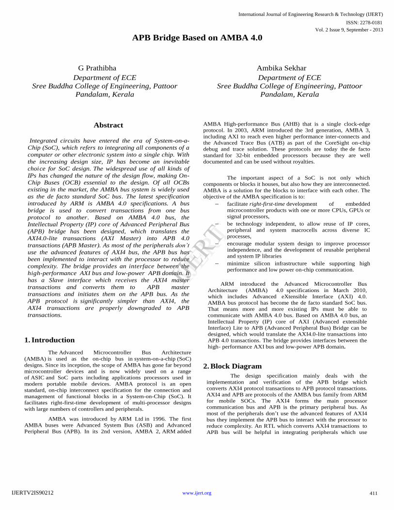
2. Block Diagram
The design specification mainly deals with the
implementation and verification of the APB bridge which
converts AXI4 protocol transactions to APB protocol transactions.
AXI4 and APB are protocols of the AMBA bus family from ARM
for mobile SOCs. The AXI4 forms the main processor
communication bus and APB is the primary peripheral bus. As
most of the peripherals don’t use the advanced features of AXI4
bus they implement the APB bus to interact with the processor to
reduce complexity. An RTL which converts AXI4 transactions to
APB bus will be helpful in integrating peripherals which use
411
International Journal of Engineering Research & Technology (IJERT)
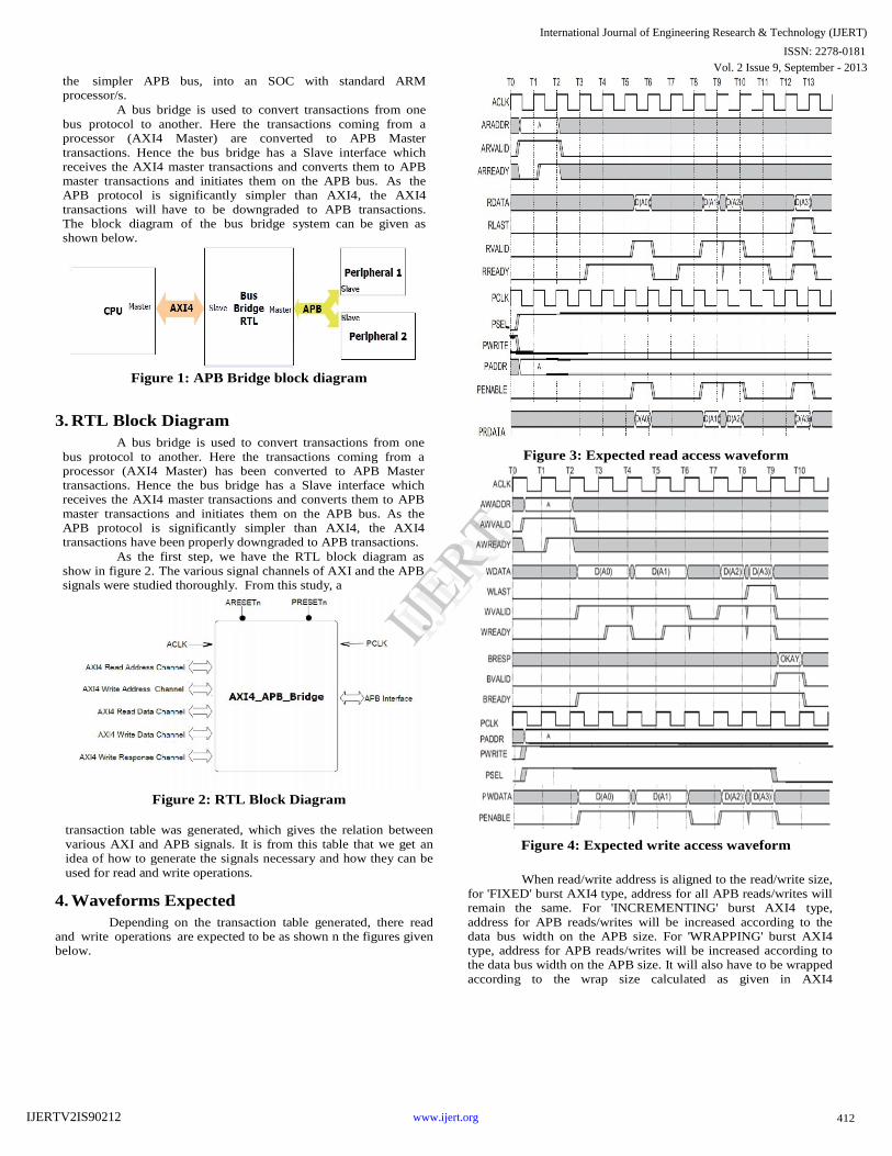
When read/write address is unaligned to the read/write
size, for 'FIXED' burst AXI4 type, address for all APB reads will
remain the same. The size of transfer should not exceed data bus
width. If system address is higher than that of master, then
higher order bits are filled with zeroes, else they are left
unconnected if narrower. For 'INCREMENTING' burst AXI4 type,
address for APB reads will be increased according to the data bus
width on the APB size. The size of transfer should not exceed data
bus width. If system address is higher than that of master, then
higher order bits are filled with zeroes, else they are left
unconnected if narrower. For 'WRAPPING' burst AXI4 type,
address for APB reads will be increased according to the data bus
width on the APB size. It will also have to be wrapped according
to the wrap size calculated as given in AXI4 specifications. The
size of transfer should not exceed data bus width. If system
address is higher than that of master, then higher order bits are
filled with zeroes, else they are left unconnected if narrower.
For AXI read/write data transactions, as APB is single
data exchange bus we will need to wait for each data to come
before we can initiate a data beat on the AXI read bus. More
complications come in if data bus size is different in AXI4 and
APB.
The write response channel signals is for letting the AXI
peripherals know about the conditions of transfer. Errors and such
related conditions will be made known.
5. Simulation and Implementation
5.1 Clock and Reset Block
As in any SoC designs, the main unit is the clock and reset
block. The purpose of this block is to generate the necessary clock and reset signals. In the APB bridge, we need two clock signals and two reset signals. ACLK and ARESETn for the AXI part and the PCLK and PRESETn for the APB part. The figure below shows the simulation result for clock and reset block.
Figure 5: Clock and reset block output
5.2 Transaction Generator Block
The purpose of this block is to generate random values
for all the signals related to AXI. For each positive edge of the
ACLK, the signals have different values. This is generated by
using the keyword $random in the verilog language.
Random values are obtained for the signals when this keyword
is used. An intermediate signal is generated for all the signals
involved in the transactions in this block.
The signal values depend on the reset value. As the
reset is an active low signal, when its value s 0, all the values for
the signals will be 0, else when the reset value is 1, random value
is generated for each clock cycle.
Figure 6: Transaction generator block output
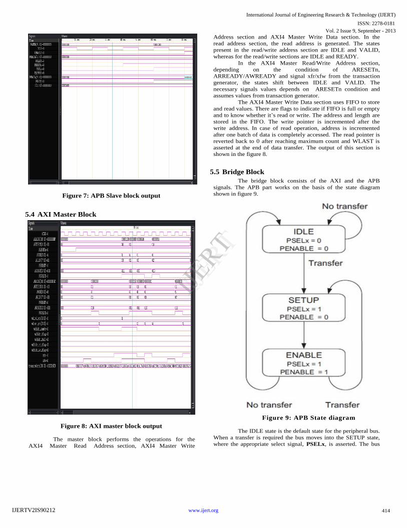
5.3 APB Slave Block
The APB slave block contains all the APB signals. The
function of this block is to check whether the function that is to be
performed by the slave is a read one or a write one. This depends
on the value of the PWRITE signal. If the value on that signal is
HGH, it’s a write process or else it’s a read process, provided
PSEL, PREADY and PENABLE are HIGH. When it’s a read
operation, the value in the memory location is read by the
PRDATA signal. When it’s a write operation, the value on the
PWDATA is written on to the memory location.
413
International Journal of Engineering Research & Technology (IJERT)


![System Verilog/UVM Verification of AMBA APB Protocol · 2021. 6. 10. · bridge (simply APB bridge) acts as the Master and initiates all the transactions [8]. This paper presents](https://static.documents.pub/doc/80x56/614869582918e2056c22abed/system-veriloguvm-verification-of-amba-apb-protocol-2021-6-10-bridge-simply.jpg)


