59
Xilinx FPGA Design Flow Ping-Liang Lai () Digital System
| Date post: | 06-Apr-2018 |
| Category: |
Documents |
| Upload: | chuanfeng-chung |
| View: | 236 times |
| Download: | 0 times |

8/3/2019 Appendix 2-FPGA Design Flow
http://slidepdf.com/reader/full/appendix-2-fpga-design-flow 1/59
Xilinx FPGA Design Flow
Ping-Liang Lai ()
Digital System

8/3/2019 Appendix 2-FPGA Design Flow
http://slidepdf.com/reader/full/appendix-2-fpga-design-flow 2/59
Outline of FPGA Design Flow
Project Navigator I: Schematic
(Project)
(Schematic)
(Functional Simulation)
» Testbench» :Modelsim Simulator
» Implementation Constraints File
» Implementation Design
» (Timing Simulation) :Modelsim Simulator
» Configuration
»
II: Verilog

8/3/2019 Appendix 2-FPGA Design Flow
http://slidepdf.com/reader/full/appendix-2-fpga-design-flow 3/59
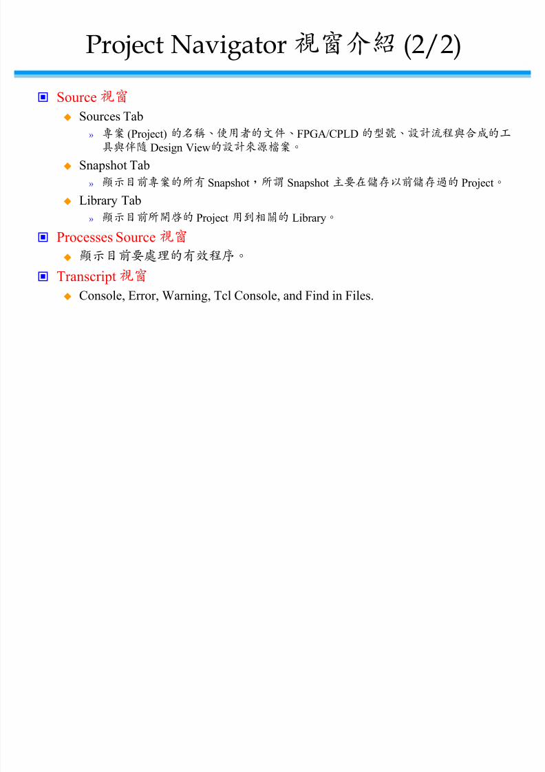
Project Navigator (1/2)
Source
Process
Source
Transcript
Multi-document Interface
8/3/2019 Appendix 2-FPGA Design Flow
http://slidepdf.com/reader/full/appendix-2-fpga-design-flow 4/59

8/3/2019 Appendix 2-FPGA Design Flow
http://slidepdf.com/reader/full/appendix-2-fpga-design-flow 5/59
Outline of FPGA Design Flow
Project Navigator I: Schematic
(Project)
(Schematic)
(Functional Simulation)
» Testbench» :Modelsim Simulator
» Implementation Constraints File
» Implementation Design
» (Timing Simulation) :Modelsim Simulator
» Configuration
»
II: Verilog

8/3/2019 Appendix 2-FPGA Design Flow
http://slidepdf.com/reader/full/appendix-2-fpga-design-flow 6/59
(1/8)
Step 1: File New Project

8/3/2019 Appendix 2-FPGA Design Flow
http://slidepdf.com/reader/full/appendix-2-fpga-design-flow 7/59
(2/8)
FPGA: Spartan 3 XC3S200-FT256

8/3/2019 Appendix 2-FPGA Design Flow
http://slidepdf.com/reader/full/appendix-2-fpga-design-flow 8/59
(3/8)
Step 2: Source Schematic

8/3/2019 Appendix 2-FPGA Design Flow
http://slidepdf.com/reader/full/appendix-2-fpga-design-flow 9/59
(4/8)
New Source Summary

8/3/2019 Appendix 2-FPGA Design Flow
http://slidepdf.com/reader/full/appendix-2-fpga-design-flow 10/59
(5/8)
We only need one Source, so Next.

8/3/2019 Appendix 2-FPGA Design Flow
http://slidepdf.com/reader/full/appendix-2-fpga-design-flow 11/59
(6/8)
We don¶t need and have any Existing Sources, so Next.

8/3/2019 Appendix 2-FPGA Design Flow
http://slidepdf.com/reader/full/appendix-2-fpga-design-flow 12/59
(7/8)
New Project Summary

8/3/2019 Appendix 2-FPGA Design Flow
http://slidepdf.com/reader/full/appendix-2-fpga-design-flow 13/59
(8/8)
1.
Source
,
Device2.

8/3/2019 Appendix 2-FPGA Design Flow
http://slidepdf.com/reader/full/appendix-2-fpga-design-flow 14/59
Outline of FPGA Design Flow
Project Navigator I: Schematic
(Project)
(Schematic)
(Functional Simulation)
» Testbench» :Modelsim Simulator
» Implementation Constraints File
» Implementation Design
» (Timing Simulation) :Modelsim Simulator
» Configuration
»
II: Verilog

8/3/2019 Appendix 2-FPGA Design Flow
http://slidepdf.com/reader/full/appendix-2-fpga-design-flow 15/59
Schematic (1/5)
Schematic
Add wireAdd Net Name
Add I/O Maker
Add Symbol

8/3/2019 Appendix 2-FPGA Design Flow
http://slidepdf.com/reader/full/appendix-2-fpga-design-flow 16/59
Schematic (2/5)
Step 3: Add Symbol and Wire.

8/3/2019 Appendix 2-FPGA Design Flow
http://slidepdf.com/reader/full/appendix-2-fpga-design-flow 17/59
Schematic (3/5)
Step 4: Add IO Maker.
8/3/2019 Appendix 2-FPGA Design Flow
http://slidepdf.com/reader/full/appendix-2-fpga-design-flow 18/59
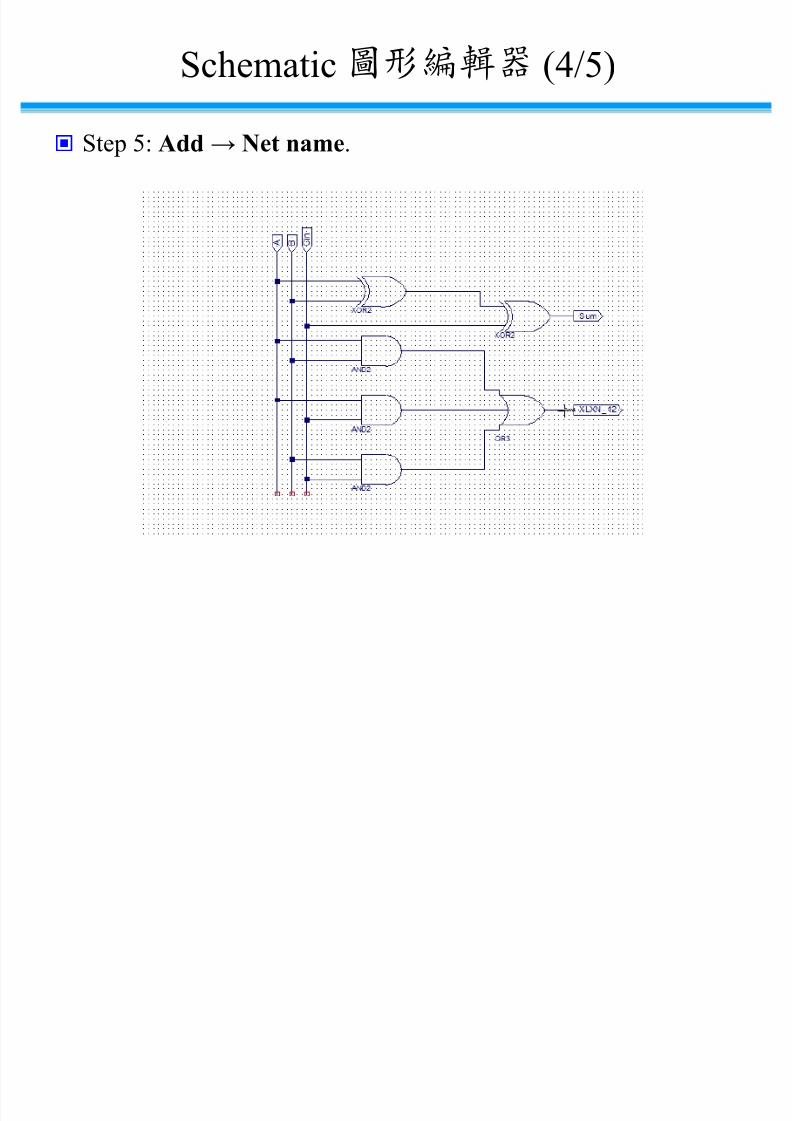
Schematic (4/5)
Step 5: Add Net name.

8/3/2019 Appendix 2-FPGA Design Flow
http://slidepdf.com/reader/full/appendix-2-fpga-design-flow 19/59
Schematic (5/5)
Step 6: Tool Check schematic, and check no error and Save.

8/3/2019 Appendix 2-FPGA Design Flow
http://slidepdf.com/reader/full/appendix-2-fpga-design-flow 20/59
Outline of FPGA Design Flow
Project Navigator I: Schematic
(Project)
(Schematic)
(Functional Simulation)
» Testbench» :Modelsim Simulator
» Implementation Constraints File
» Implementation Design
» (Timing Simulation) :Modelsim Simulator
» Configuration
»
II: Verilog
8/3/2019 Appendix 2-FPGA Design Flow
http://slidepdf.com/reader/full/appendix-2-fpga-design-flow 21/59
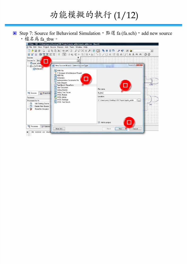
(1/12)
Step 7: Source for Behavioral Simulation fa (fa.sch)add new source fa_tbw

8/3/2019 Appendix 2-FPGA Design Flow
http://slidepdf.com/reader/full/appendix-2-fpga-design-flow 22/59
(2/12)
We only have one source, so Next.

8/3/2019 Appendix 2-FPGA Design Flow
http://slidepdf.com/reader/full/appendix-2-fpga-design-flow 23/59
(3/3)
New Source Summary
8/3/2019 Appendix 2-FPGA Design Flow
http://slidepdf.com/reader/full/appendix-2-fpga-design-flow 24/59
(4/12)
8/3/2019 Appendix 2-FPGA Design Flow
http://slidepdf.com/reader/full/appendix-2-fpga-design-flow 25/59
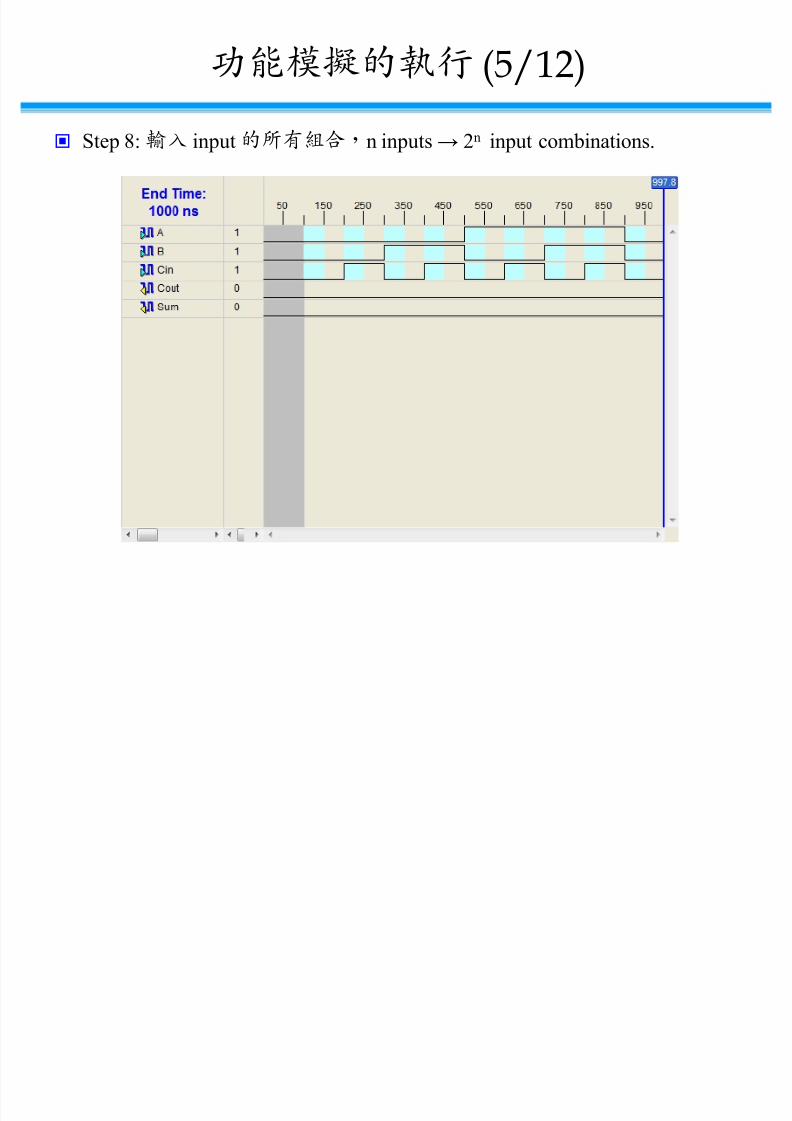
(5/12)
Step 8: inputn inputs 2n input combinations.

8/3/2019 Appendix 2-FPGA Design Flow
http://slidepdf.com/reader/full/appendix-2-fpga-design-flow 26/59
(6/12)
Step 9: Modelsim Simulator Simulate Behavioral Model (Double click mouse left key 2 times).
8/3/2019 Appendix 2-FPGA Design Flow
http://slidepdf.com/reader/full/appendix-2-fpga-design-flow 27/59
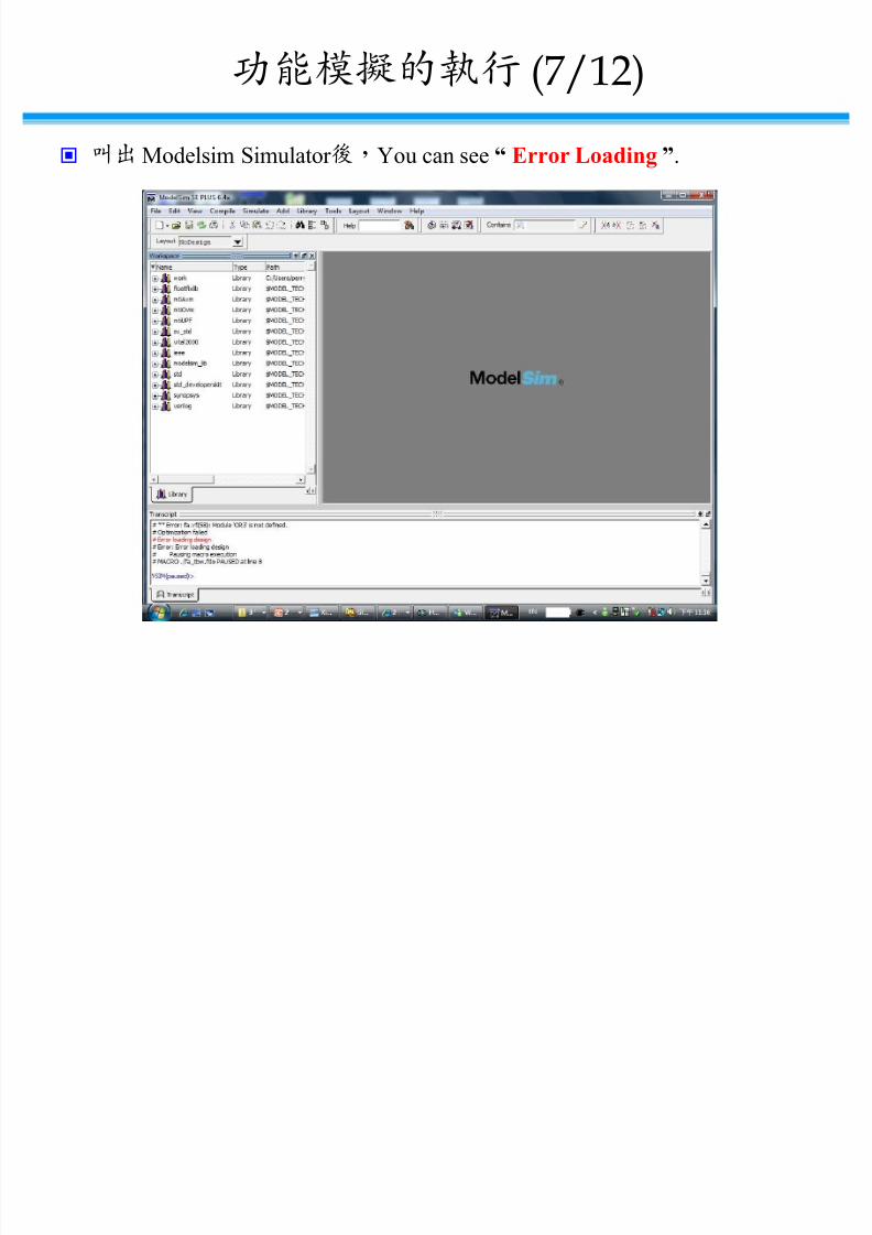
(7/12)
Modelsim Simulator You can see ³ Error Loading ´.

8/3/2019 Appendix 2-FPGA Design Flow
http://slidepdf.com/reader/full/appendix-2-fpga-design-flow 28/59
(8/12)
Step 10: Select work Compiler A ND2, OR3, and XOR2. (file path:C://Xilinx/9.2i/ISE/verilog/src/unisims)

8/3/2019 Appendix 2-FPGA Design Flow
http://slidepdf.com/reader/full/appendix-2-fpga-design-flow 29/59
(9/12)
Step 11: In fa_tbw, Right click Simulate
8/3/2019 Appendix 2-FPGA Design Flow
http://slidepdf.com/reader/full/appendix-2-fpga-design-flow 30/59
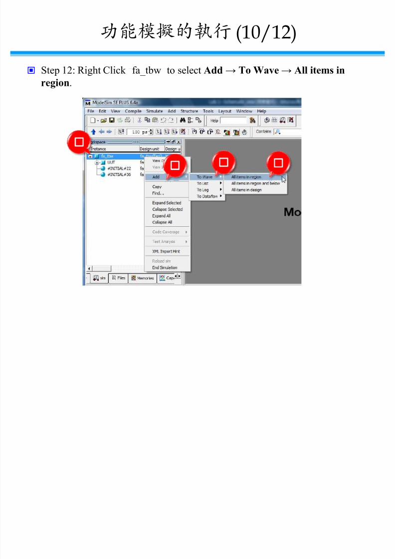
(10/12)
Step 12: Right Click ³fa_tbw
´to select Add To Wave All items in
region.

8/3/2019 Appendix 2-FPGA Design Flow
http://slidepdf.com/reader/full/appendix-2-fpga-design-flow 31/59
(11/12)
Behavioral Waveform Window

8/3/2019 Appendix 2-FPGA Design Flow
http://slidepdf.com/reader/full/appendix-2-fpga-design-flow 32/59
(12/12)
Step 14: Run all, and Step 15: Zoom fit.

8/3/2019 Appendix 2-FPGA Design Flow
http://slidepdf.com/reader/full/appendix-2-fpga-design-flow 33/59
Outline of FPGA Design Flow
Project Navigator I: Schematic
(Project)
(Schematic)
(Functional Simulation)
» Testbench» :Modelsim Simulator
» Implementation Constraints File
» Implementation Design
» (Timing Simulation) :Modelsim Simulator
» Configuration
»
II: Verilog

8/3/2019 Appendix 2-FPGA Design Flow
http://slidepdf.com/reader/full/appendix-2-fpga-design-flow 34/59
Implementation Constraints File (1/8)
Step16: Sources for ³ Synthesis/Implementation ³ Step 17: fa.schProject New Source

8/3/2019 Appendix 2-FPGA Design Flow
http://slidepdf.com/reader/full/appendix-2-fpga-design-flow 35/59
Implementation Constraints File (2/8)

8/3/2019 Appendix 2-FPGA Design Flow
http://slidepdf.com/reader/full/appendix-2-fpga-design-flow 36/59
Implementation Constraints File (3/8)
Step 18: fa.ucf User Constraints Assign Package Pins.
8/3/2019 Appendix 2-FPGA Design Flow
http://slidepdf.com/reader/full/appendix-2-fpga-design-flow 37/59
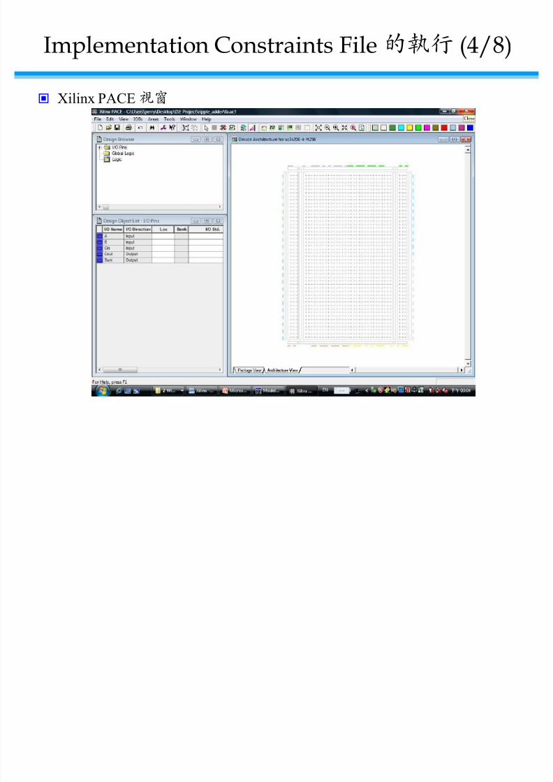
Implementation Constraints File (4/8)
Xilinx PACE

8/3/2019 Appendix 2-FPGA Design Flow
http://slidepdf.com/reader/full/appendix-2-fpga-design-flow 38/59
Implementation Constraints File (5/8)
Step 19:Package ViewDesign Browser I/O Pins

8/3/2019 Appendix 2-FPGA Design Flow
http://slidepdf.com/reader/full/appendix-2-fpga-design-flow 39/59
Implementation Constraints File (6/8)
Step 20: Spartan-3 FPGA XC3S200-FT256 Datasheet Slide Switches
LEDs

8/3/2019 Appendix 2-FPGA Design Flow
http://slidepdf.com/reader/full/appendix-2-fpga-design-flow 40/59
Implementation Constraints File (7/8)
File Save

8/3/2019 Appendix 2-FPGA Design Flow
http://slidepdf.com/reader/full/appendix-2-fpga-design-flow 41/59
Implementation Constraints File (8/8)
Edit Constraints (Text)

8/3/2019 Appendix 2-FPGA Design Flow
http://slidepdf.com/reader/full/appendix-2-fpga-design-flow 42/59
Outline of FPGA Design Flow
Project Navigator I: Schematic
(Project)
(Schematic)
(Functional Simulation)
» Testbench» :Modelsim Simulator
» Implementation Constraints File
» Implementation Design
» (Timing Simulation) :Modelsim Simulator
» Configuration »
II: Verilog

8/3/2019 Appendix 2-FPGA Design Flow
http://slidepdf.com/reader/full/appendix-2-fpga-design-flow 43/59
Implement Design (1/6)
Step 21: Implement Design

8/3/2019 Appendix 2-FPGA Design Flow
http://slidepdf.com/reader/full/appendix-2-fpga-design-flow 44/59
Implement Design (2/6)

8/3/2019 Appendix 2-FPGA Design Flow
http://slidepdf.com/reader/full/appendix-2-fpga-design-flow 45/59
Implement Design (3/6)
Place & Route View/Edit Routed Design (FPGA Editor) LUT
8/3/2019 Appendix 2-FPGA Design Flow
http://slidepdf.com/reader/full/appendix-2-fpga-design-flow 46/59
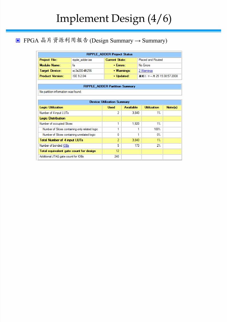
Implement Design (4/6)
FPGA (Design Summary Summary)

8/3/2019 Appendix 2-FPGA Design Flow
http://slidepdf.com/reader/full/appendix-2-fpga-design-flow 47/59
Implement Design (5/6)
Pinoout Report (Design Summary Pinout Report)

8/3/2019 Appendix 2-FPGA Design Flow
http://slidepdf.com/reader/full/appendix-2-fpga-design-flow 48/59
Implement Design (6/6)
: Generate Post-Place & Route Static Timing AnalyzePost-Place & Route Static Timing.

8/3/2019 Appendix 2-FPGA Design Flow
http://slidepdf.com/reader/full/appendix-2-fpga-design-flow 49/59
Outline of FPGA Design Flow
Project Navigator I: Schematic
(Project)
(Schematic)
(Functional Simulation)
» Testbench» :Modelsim Simulator
» Implementation Constraints File
» Implementation Design
» (Timing Simulation) :Modelsim Simulator
» Configuration »
II: Verilog

8/3/2019 Appendix 2-FPGA Design Flow
http://slidepdf.com/reader/full/appendix-2-fpga-design-flow 50/59
(Timing Simulation)
Functional Simulation

8/3/2019 Appendix 2-FPGA Design Flow
http://slidepdf.com/reader/full/appendix-2-fpga-design-flow 51/59
Outline of FPGA Design Flow
Project Navigator I: Schematic
(Project)
(Schematic)
(Functional Simulation)
» Testbench» :Modelsim Simulator
» Implementation Constraints File
» Implementation Design
» (Timing Simulation) :Modelsim Simulator
» Configuration »
II: Verilog

8/3/2019 Appendix 2-FPGA Design Flow
http://slidepdf.com/reader/full/appendix-2-fpga-design-flow 52/59
Configuration (1/2)
Step 22: Generate Programming File

8/3/2019 Appendix 2-FPGA Design Flow
http://slidepdf.com/reader/full/appendix-2-fpga-design-flow 53/59
Configuration (2/2)
Configure Device (iMPACT) Step 22: iMPACT Configure devices using Boundary-Scan
(JTAG) Automatically «

8/3/2019 Appendix 2-FPGA Design Flow
http://slidepdf.com/reader/full/appendix-2-fpga-design-flow 54/59
Outline of FPGA Design Flow
Project Navigator I: Schematic
(Project)
(Schematic)
(Functional Simulation)
» Testbench» :Modelsim Simulator
» Implementation Constraints File
» Implementation Design
» (Timing Simulation) :Modelsim Simulator
» Configuration »
II: Verilog

8/3/2019 Appendix 2-FPGA Design Flow
http://slidepdf.com/reader/full/appendix-2-fpga-design-flow 55/59
II: Verilog
From Step 2 to choose a Verilog Module, and repeat Step3 ~ Step 22. Design example: 4-bit Ripple Carry Counter

8/3/2019 Appendix 2-FPGA Design Flow
http://slidepdf.com/reader/full/appendix-2-fpga-design-flow 56/59
reset ck qn qn+1
1 * 1 0
1 * 0 0
0 0 1
0 1 0

8/3/2019 Appendix 2-FPGA Design Flow
http://slidepdf.com/reader/full/appendix-2-fpga-design-flow 57/59

8/3/2019 Appendix 2-FPGA Design Flow
http://slidepdf.com/reader/full/appendix-2-fpga-design-flow 58/59

8/3/2019 Appendix 2-FPGA Design Flow
http://slidepdf.com/reader/full/appendix-2-fpga-design-flow 59/59


