Page 1
Appendix A
Fabrication and Packaging
Here we describe the microfabrication process developed in the course of this work
for the fabrication of various prototypes reported in this dissertation. The reported
fabrication process, developed based on the previous single-mask die-level process
from [5] and wafer-level DRIE recipe optimization from [135], is a two mask SOI
process with patterned metal wirebonding pads and traces on the front side and
blanket metallization of the wafer backside for packaging and die attachment.
1. Substrate specification.
• SOI wafer details: Typical characteristics of the SOI wafers used in the
process are summarized in Table A.1. The suggested vendor is Thomas
Table A.1: Typical parameters of the SOI wafers.
Parameter, units ValueWafer diameter, mm 100Device layer thickness, µm 50Device layer resistivity, Ω-cm 0.01-0.03Device layer type P/B, (1-0-0)Surface finish type double-sided polishedBuried oxide (BOX) thickness, µm 5Handle layer thickness, µm 500Device layer resistivity, Ω-cm 10 to 100 rangeDevice layer type P/B, (1-0-0)
227
Page 2
Gentemann, Ultrasil Corporation, (510)-266-3700, [email protected] ,
http://www.ultrasil.com/. Other vendors, especially Silicon Quest Inter-
national (SQI) are strongly discouraged. When ordering the SOI wafers,
make sure their fabrication is done by bonding an oxidized wafer to a sili-
con wafer, NOT by oxide-to-oxide bonding of pairs of two oxidized silicon
wafers.
2. Blanket metallization of the SOI wafer backside (handle layer) for packaging.
• Clean the wafer: Rinse with acetone. Rinse with isopropanol. Rinse
with DI water. Remove surface oxides using a 20 % or less concentrated
HF bath for 30 seconds. Rinse in DI water. Blow-dry with nitrogen.
At this point water should easily bead-up and come off the hydrophobic
surface of the exposed silicon.
• Deposit metal: E-beam evaporate 500 A chromium adhesion layer and
5000 A gold layer. The outer gold layer provides a corrosion-resistant
interface for eutectic bonding and electrical connectivity for the wafer’s
handle layer.
3. Lift-off metallization∗ of the SOI wafer front-side (device layer).
• Clean the wafer: Repeat the cleaning procedure described above. De-
hydrate the wafer using a 90 to 120 nitrogen dehydration oven for at
least 30 minutes.
• Lithography for lift-off: Spin-coat Shipley 1827 on the front side of the
wafer at 2500 RPM; do not use any adhesion promoter! Soft-bake in 90
∗The described lift-off recipe was suggested by Mo Kebaili, Kebaili Corporation,http://www.kebaili.com.
228
Page 3
oven for 30 minutes. Expose in MA-6 for 25 seconds. Soak in chlorobenzene
for 3-4 min. Nitrogen dry-blow, do not rinse! Develop in MF-319 for 45
seconds. Rinse in DI water, nitrogen dry-blow. The photoresist mask
should be 3 to 4 µm thick, which is sufficient for metal thicknesses below 1
µm. Swelling of the photoresist due to the chlorobenzene exposure ensures
the overhanging profile needed for correct lift-off.
• Deposit metal: E-beam evaporate 500 A chromium adhesion layer and
5000 A gold layer. The gold provides an interface for device wire-bonding.
• Lift-off metal: Soak the wafer for several hours in acetone, Figure A.1.
Rinse with isopropanol and nitrogen blow-dry, Figure A.2.
4. DRIE etching of the SOI wafer device layer.
• Clean the wafer: Repeat the cleaning procedure described above. De-
hydrate the wafer using a 90 to 120 nitrogen dehydration oven for at
least 30 minutes.
• Lithography for DRIE: Program the spinner for 20 seconds at 500 RPM
followed by 40 seconds at 5000 RPM (use moderate acceleration). Spin-
coat adhesion promoter HMDS on on the front side of the wafer. Spin-coat
AZ-4620 photoresist. Soft-bake in 90 oven for 20 minutes. Use MA-6 to
align the device mask to the alignment marks defined in the metal lift-off
step; expose for 30 to 35 seconds. Develop in 4:1 water:AZ-400 (by volume)
solution for several minutes. Rinse in DI water, nitrogen dry-blow. The
photoresist mask should be around 6 µm thick, which is sufficient for at
leat 50 µm deep DRIE. Reduce the second stage of the spinning to 3000
RPM (corresponding to about 10 µm thick photoresist) if a 100 µm DRIE
is needed.
229
Page 4
• DRIE: Etch the device layer of the SOI wafer in the STS ASE tool using
the “Alex6R1” recipe (first and last step is etch, 13 s etch, 8 s passivation,
manual APC at 70 %). The etch rate of the process is approximately 0.5
µm/min; for 50 µm device thickness use 105 to 110 etching cycles. Do not
overetch the wafers, as this will cause severe undercutting of structures,
possible dry-release, and inability to correctly release the structures in the
HF bath.
• Photoresist removal: Soak the wafer in acetone for 10 minutes. Rinse
with acetone and isopropanol. Nitrogen blow-dry. Use an oxygen plasma
tool to remove the photoresist residue. Set the pressure to 200 mTorr.
Gradually ramp the power up to 200 W. Keep for half an hour or until all
the photoresist residue is removed, Figure A.3.
5. Wafer dicing.
• Prepare for dicing: Spin-coat a thick layer, ≈10 µm, of AZ-4620 pho-
toresist. Soft-bake in 90 oven for 15 minutes.
• Dicing: Ship the prepared wafer for professional dicing and provide a dic-
ing map. The suggested vendor is Jeff Olson, Spectrum Micromechanical,
Inc. 858 395-2264, http://spmmi.com.
• Extracting dies: The diced wafer is typically shipped back attached to
a stretched blue tape circle, Figure A.4. Extract the individual dies by
gently pushing on the backside of the blue tape with tweezers.
• Dies cleaning: Clean the individual dies by soaking for 10 minutes in ace-
tone twice, followed by a isopropanol bath. Shake of the excess isopropanol
from the dies and let them dry on a cleanroom wipe, Figure A.5.
230
Page 5
6. Wet release of the fabricated devices.
• HF bath: Collect 10-20 dies in a HF-proof perforated basket. Soak the
devices in a 20 % HF solution for approximately 45 minutes (the timing is
design dependent).
• Dies cleaning: Extract the basket from the HF bath. Soak and rinse in
DI water. Soak in warm isopropanol.
• Dies drying: Pick the dies from the warm isopropanol bath, place them
on a cleanroom wipe, let them dry. Figure A.6 shows an SEM micrograph
of a fabricated 50 µm thick gyroscope with 5 µm minimal features and
capacitive gaps.
7. Device packaging and wirebonding.
• Die attachment: Attach individual dies to the ceramic packages using
SEM carbon tape adhesive (fast and recyclable, but not rigid and vacuum
sealing compliant), epoxy (not easily recyclable, medium rigidity, generally
not vacuum sealing compliant), or eutectic preform (rigid, vacuum sealing
compliant) die attachment as discussed in [135]. A good point of contact on
eutectic packaging topics is David Virissimo of Semiconductor Packaging
Materials.
• Wirebonding: Wirebond the devices to provide electrical connectivity
from the package leads, Figure A.7 Use a wedge bonder with 1 mil Al
wire with 1 % Si from Kulicke & Soffa Industries, 1-800-422-5542, cust-
[email protected] , http://www.kns.com/. The suggested resource for all other
wirebonding questions, supplies, and services is George Garcia, PG Enter-
prises, Inc., http://www.pgent.net/.
231
Page 6
• Lid sealing: Seal the package cavity containing a wirebonded MEMS de-
vice using kovar lids with pre-deposited eutectic (“combo lids”) in ambient
or vacuum environment, Figure A.8. Consult [135] for detailed informa-
tion on the eutectic packaging and sealing process. Suggested vendor for
package-level vacuum sealing is Paul Barnes, SST International, 562-803-
3361, [email protected] , http://www.sstinternational.com/.
This completes the fabrication and packaging process. The devices are now ready
for experimental characterization using the extensive available package-level infras-
tructure.
232
Page 7
Figure A.1: Photograph of a wafer during lift-off.
Figure A.2: Photograph of a wafer after lift-off.
233
Page 8
Figure A.3: Photograph of a fabricated SOI wafer with approximately 400 individualMEMS devices designed in 3.5 mm dies.
Figure A.4: Photograph of a diced wafer.
234
Page 9
Figure A.5: Photograph of cleaned dies. Gyroscopes [34, 60, 88] implemented in 3.5mm die size are visible.
Figure A.6: SEM micrograph of a fabricated MEMS gyroscope [112,124]. The lateralcomb electrode fingers are 5 µm wide with 5 µm spacing.
235
Page 10
Figure A.7: Photograph of a gyroscope [60] die eutectically attached to a J-Leadceramic package and wirebonded.
Figure A.8: Photograph of a eutectically sealed package containing a gyroscope die.
236
Page 11
Appendix B
Stand-Alone DSP for VersatileMEMS Characterization
This chapter reports a stand-alone signal processing and control unit designed to pro-
vide flexible characterization of MEMS vibratory gyroscopes. The unit consists of a
programmable 32-bit 150 MIPS DSP controller, 16-bit 1 MSPS digital-to-analog and
18-bit analog-to-digital interface circuits, and signal conditioning electronics. The
multi-channel analog-to-digital interface is optimized for detection of small electrical
signals typical for MEMS devices. Digitally controlled conditioning of analog signals
allows for high-resolution differential digitization of a wide range of detection signals.
The digital-to-analog interface circuit produces a wide range of DC and AC voltages
needed for actuation and detection in gyroscopes; a single 5 V supply is used to
power the board. The DSP controller allows easy MATLAB/Simulink programming
and execution-time data exchange. Performance of the board was experimentally
characterized using an anti-phase driven rate gyroscope with multi-degree of freedom
sense mode. Using 16-bit conversion, the measured capacitance-change equivalent res-
olution is 27 aF/√
Hz. Due to its flexible architecture, the unit is easily customizable
for stand-alone and computer controlled operation of a variety of dynamic MEMS.
237
Page 12
B.1 Introduction
Discrete bench-top instruments such as dynamic signal analyzers and lock-in ampli-
fiers are often used for initial structural and Coriolis characterization of microma-
chined gyroscopes [26, 136]. However, this approach is not practical for stand-alone
field-testing of prototypes and does not allow fast and flexible evaluation of different
actuation, detection and control algorithms. General-purpose Digital Signal Process-
ing (DSP) systems such as dSPACE and National Instruments Compact RIO can
provide a powerful control solution, but have limited portability, are costly and not
optimized to interface capacitive MEMS. Custom made integrated and Printed Cir-
cuit Board (PCB) level electronics are commonly used for stand-alone operation of
gyroscopes [10, 11]; however, change of operational parameters or signal processing
and control algorithms often involves circuit re-design and reassembly with different
electrical components. In this work, we report an easily programmable and computer-
interfaced yet compact signal processing and control platform for capacitive micro-
machined gyroscopes and other dynamic MEMS.
B.2 Electronics Design
The main hardware components of the proposed platform are a programmable DSP
controller, digital-to-analog and analog-to-digital interface circuits equipped with sig-
nal conditioning analog electronics, see Figure B.1. The unit was assembled using off
the shelf components on a single 112 by 87 mm six-layer PCB. Below we discuss design
and implementation of the major circuit blocks and choice of particular components.
The main properties of the unit are summarized in Table B.1.
238
Page 13
Figure B.1: Block diagram of the main hardware components.
B.2.1 Processor
A highly integrated Texas Instruments TMS320F2812 single-chip DSP controller was
chosen for the board due to its performance/cost efficiency. This DSP has a maxi-
mum internal frequency of 150 MHz (i.e., 6.67 ns cycle time) stabilized by a 30 MHz
external quartz resonator, and is equipped with 128 K x 16 Flash memory, 18 K
x 16 Single-Access RAM (SARAM). A 16-bit bus with independent data and ad-
dress transmission lines interfaces the processor with on-board DACs and ADCs. A
Serial Peripheral Interface (SPI) and discrete glue logic is used to digitally control
potentiometers in the independent analog signal conditioning circuits. The board is
linked to a host computer for execution-time data exchange and adjustment of signal
processing parameters using an external RS-232C transceiver and an internal Serial
Table B.1: Main operational parameters of the DSP board.
Functional Subsystem CharacteristicsDSP controller TI TMS320F2812 32-bit 150 MIPSADC and DAC conversion update rate 100 kHz2 DACs AC carrier channels 10 Vpp, 0.15 mV step2 DACs AC+DC actuation channels ±100 V, 0.8 mV step3 DACs monitor channels 10 Vpp, 0.15 mV step3 differential I-to-V ADCs 1-10 MΩ gain, 18-bit
239
Page 14
Communication Interface (SCI). Programming of the processor is done using a JTAG
port.
B.2.2 Digital-to-Analog Interface Circuit
The purpose of the digital-to-analog interface circuit is to convert the digital signals
generated by the processor into analog waveforms to control gyroscopes and to provide
connectivity to external measurement equipment. Based on the high-speed 1 MSPS
16-bit digital-to-analog converter (DAC) TI DAC8820, three types of digital-to-analog
interface circuits with different analog signal conditioning were incorporated on the
board.
Two identical but independent actuation channels were designed in order to ac-
commodate gyroscopes with multi-degree of freedom drive modes. Each of the chan-
nels consists of a DAC and an additional circuit, which amplifies the generated analog
signal and adds a digitally controlled DC bias. These control channels are able to
output arbitrary waveform actuation voltages in the range from 0 to ±100 V.
Two additional arbitrary waveform low-voltage (-5 to +5 V) channels each based
on a simple buffer at the DAC output were also designed to provide accurate probing
voltages (carriers) necessary for detection of motion in dynamic microstructures.
A separate group of DAC channels was implemented to enable connectivity of the
DSP board to external measurement equipment, such as dynamic signal analyzers,
for debugging of algorithms and monitoring of experiments in real time. In these
channels, the DACs are followed by high quality four-pole Low-Pass Filters (LPF) to
suppress the sampling rate signal. The output signals range from -5 to +5 V.
240
Page 15
B.2.3 Analog-to-Digital Interface Circuit
Capacitive sensing of drive and sense mode vibratory motion in gyroscopes is typ-
ically based on measuring the current induced by the relative motion of capacitive
electrodes. To accurately digitize pick-up currents from microgyroscopes, three inde-
pendent channels were designed and implemented each based on a three-stage fully
differential transimpedance amplifier and a high speed 18-bit ADC.
The three amplification stages are based on TI THS4141 high-speed fully differ-
ential amplifiers with 84 dB common mode rejection. The first stage converts the
difference of the input currents into a voltage difference across its two outputs with
a digitally controlled transimpedance gain of 100 - 110 kΩ. The second stage is a
fully differential two-pole anti-aliasing LPF with the -3 dB cutoff frequency of ap-
proximately 50 kHz. The last stage is a variable gain voltage amplifier. The gain is
defined by Digitally Controlled Potentiometers (DCP) AD5290 and can range from
0 to 20 dB. A high-speed ADC TI ADS8482 was used in each detection channel to
convert the analog voltage difference to the digital code with a sampling rate up to 1
MSPS.
B.2.4 Power Handling
A single +5 V stabilized external DC voltage source powers the board. All other
voltage levels necessary for operation are formed on the board by the dedicated power
converters. To power the analog amplifiers, an additional -5 V voltage is generated
onboard. A pair of -100 and +100 V is also generated to power the high-voltage
amplifiers in the control voltage channels. An additional +1.9 V is used to power the
DSP core, and +3.3 V is used for the digital circuits.
241
Page 16
Figure B.2: A photograph of an assembled controller board with a packaged gyro-scope.
B.3 Experimental Characterization
In this section we report preliminary characterization of both drive and sense mode
functionality of the board with a MEMS gyroscope using electromechanical amplitude
modulation (EAM) detection technique, see, for example, [58]. Figure B.2 shows
a photograph of a fully assembled signal processing unit and highlights its main
components.
B.3.1 Hardware and Software Configuration
The onboard ADCs were configured for 16-bit conversions. A MATLAB-based Graph-
ical User Interface (GUI) was developed for the real-time control of the transimpedance
gains, value of the DC component of the driving voltage, as well as amplitudes and fre-
quencies of the AC driving and carrier voltages. The interface can be easily modified
to control any run-time variables.
242
Page 17
Figure B.3: SEM of the gyroscope used for the experimental evaluation of the board.
B.3.2 Test Device
An anti-phase driven rate gyroscope with multi-degree of freedom sense mode [60,88]
was used for the experiments. The gyroscope’s drive mode consists of two coupled
frames driven into anti-phase resonance using a common lateral comb drive electrode
in the center of the device. Two separate 2-DOF sense mode resonators are located
inside of the drive mode decoupling frames. The drive mode resonant frequency is
designed to be in-between the 2-DOF sense mode resonant frequencies for robust off-
resonant operation and anti-phase detection of the input angular rate. Figure B.3
shows an SEM of a device fabricated in-house using an SOI process. The gyroscope
was packaged and wire-bonded in a CDIP-24 package and tested in atmospheric pres-
sure (drive-mode quality factor was approximately 300, sense-mode effective quality
factors were approximately 40).
243
Page 18
B.3.3 Drive-Mode Detection
In order to actuate the anti-phase motion in the drive mode of the gyroscope, a
driving voltage was applied to the central anchored lateral comb electrode. The
drive voltage consisted of a 37.5 V DC bias and an AC component at the 1.568
kHz resonant frequency of the device. Using the real-time computer graphical user
interface, the amplitude of the AC driving component was adjusted to 14.75 V to
achieve the vibration with a nominal 6 µm amplitude. A 5 V AC carrier voltage at
20 kHz frequency was applied to the movable mass of the gyroscope to enable EAM
detection of motion.
Anti-phase motion of the gyroscope’s decoupling frames was detected using drive-
mode parallel plate detection capacitors. The pick-up currents from the anchored
electrodes were amplified using the on-board three-stage differential transimpedance
amplifier and digitized. Figure B.4 shows Power Spectral Density (PSD) of the drive-
mode pick-up signals for the cases of single-sided and fully differential capacitive
detection. The single-sided detection signal contains feed-through of drive and carrier
AC voltages, as well as multiple informational sidebands inherent to parallel plate
detection of sinusoidal motion [58].
Differential detection with independently tuned gains has several practical ad-
vantages. Unwanted parasitic feed-through of the drive AC signal was suppressed by
almost 20 dB. Also, the white noise floor was improved by approximately 10 dB. Most
importantly, the 20 kHz carrier signal was suppressed by more than 30 dB to the level
below the main informational sidebands, thus improving the useable dynamic range.
In the described experiment, the nominal parallel plate sense capacitance of the
gyroscope’s drive mode was 0.22 pF. During the 6 µm amplitude vibration, the main
harmonic of the parallel plate capacitance change had an amplitude of 0.15 pF [58].
244
Page 19
5 10 15 20 25
−100
−80
−60
−40
−20
0
Frequency, kHz
PS
D, d
BV
rms/
rt−
Hz
32 d
B
single−sided differential
Drive, 1.57 kHz
Carrier
Main EAM Sidebands−45 dBVrms/rt−Hz
Noise Floor −100 dBVrms/rt−Hz
Figure B.4: Experimentally measured PSD of the drive-mode modulated pick-upsignal during 6 µm amplitude vibrations.
For the tested gyroscope, the measured displacement-equivalent resolution was 1.13
nm/√
Hz. By normalizing to the gyroscope’s parameters, capacitance-change equiv-
alent resolution of the board with 16-bit ADC was derived to be 0.027 fF/√
Hz.
B.3.4 Sense-Mode Detection
Preliminary characterization of the Coriolis detection functionality of the board was
also performed using the anti-phase driven gyroscope [60,88]. Actuation of the drive
mode vibration was done as in the previously described experiments; the detection
channels were switched from the drive mode to the two differential sense mode capac-
itors inside one of the decoupling frames. The board was mounted on a rate table,
which was configured to produce sinusoidal rotation of a fixed amplitude and fre-
quency. Two different experiments were performed: 3.6 rotation at 5 Hz frequency,
and 7.2 rotation at 2.5 Hz frequency. In both cases, the amplitude of the applied
245
Page 20
18.48 18.485 18.49−75
−70
−65
−60
−55
−50
−45
−40
Frequency, kHz
PS
D, d
BV
rms/
rt−
Hz
18 d
eg/s
sin
usoi
d
7.2 deg at 2.5 Hz3.6 deg at 5 Hz
Quadrature, 40 deg/s
5 Hz2.5 Hz
Figure B.5: Experimentally measured PSD of the sense-mode modulated pick-upsignal during sinusoidal rotation.
sinusoidal angular rate was 18 /s.
Figure B.5 shows PSD of the sense-mode pick-up signal around the left informa-
tional sideband. In each experiment, the signal contains two angular rate-modulated
sidebands, and a 40 /s uncompensated quadrature. The demonstrated resolution
is sufficient for scale factor characterization of gyroscopes in various temperature
and pressure conditions; it can be improved by using the built-in 18-bit conversion
capability, performing demodulation of the EAM signal digitally before outputting
analog measurements, increasing the maximum transimpedance gains, and increasing
amplitude and frequency of the carrier AC voltage.
246
Page 21
Appendix C
Velocity-FeedbackSelf-Resonance with Carrier
This chapter highlights the development of a self-resonant drive-mode loop based on
velocity feedback with Electromechanical Amplitude Modulation (EAM). Drive-mode
of vibratory gyroscopes should be excited at the resonant frequency to provide the
highest amplitude of drive-mode motion for a given amount of driving voltages. Also,
maintaining the resonant phase condition in the drive-mode is beneficial for phase
based suppression of quadrature signals.
C.1 Phase Control and Velocity Feedback
There are two different approaches to resonant closed-loop operation of a microma-
chined oscillator. The first possible approach to resonant excitation relies on a voltage
controlled oscillator (VCO) and phase detection using a PLL or dual-phase demodu-
lation [137]. The second approach, common in micromachined oscillators, is based on
self-resonant motion excited by velocity-feedback closed loop. Simply put, velocity
feedback with sufficiently high gain turns a linear system with positive damping into
a system with negative damping; in practical implementations the system contains
nonlinearities, such as saturation, that prevent the infinite growth of the amplitude of
247
Page 22
motion. The velocity feedback approach allows to eliminate the external VCO from
the system and guarantees excitation at the resonant frequency. The potential dis-
advantages of the velocity feedback self-resonance approach include the phase noise
in the Coriolis demodulation reference signal as well as the difficulty in accurately
modeling and selecting the feedback gains.
C.2 Velocity Feedback Self-Resonance
The VCO approach with an amplitude control, also known as automatic gain control
(AGC), is discussed in [135]. Here we focus on design of the velocity feedback self-
resonant loop based on electromechanical amplitude modulation. The approach is
demonstrated using an analog circuit assembled on a breadboard using off the shelf
components, Figure C.1. A MATLAB/Simulink model of the velocity feedback loop
with EAM was created and used to provide additional insight into the closed loop
dynamics of the analog circuit velocity feedback circuit, Figure C.2.
C.3 Analog Circuit Design
The overall circuit consists of several different functional blocks. The EAM carrier
voltage is generated on-board using an XR2206 function generator IC and is applied
directly to the device. The carrier generation circuit blocks allow to adjust the signal
frequency and amplitude in from 73 to 84 kHz and from 0.5 to 8 Vrms, respectively.
The carrier block outputs a sinusoidal waveform applied to the micromachined de-
vice, as well as a 90 phase shifted square waveform used as a carrier demodulation
reference.
The drive mode detection is performed using a differential amplification stage
248
Page 23
Figure C.1: Analog implementation of the self resonant loop with EAM.
Velocity Feedback Self-Resonance
Simulation parameters
– 1 kHz natural freq.– 103 Quality factor
Simulink model: settling time ~50 ms
10/84Figure C.2: Simulink model of the velocity feedback loop.
249
Page 24
Figure C.3: Differential driving circuit block.
followed by a high pass filter to eliminate the feed-through signal. This signal is then
mixed with the carrier reference and low pass filtered to obtain the motional drive
mode voltage. This signal is then amplified, phase shifted, coupled to a DC voltage
in a differential manner, as illustrated in Figure C.3. The drive block utilizes a simple
RC circuit for AC plus DC coupling and provides low distortion of AC phase (<1
for frequencies above 0.1 kHz). Finally, the differential voltages and applied to the
device closing the loop.
C.4 Experimental Demonstration
The developed circuit for velocity feedback self-resonant drive-mode excitation using
EAM was experimentally demonstrated and characterized using an anti-phase driven
micromachined gyroscope [131] in air. The external DC drive voltage was gradually
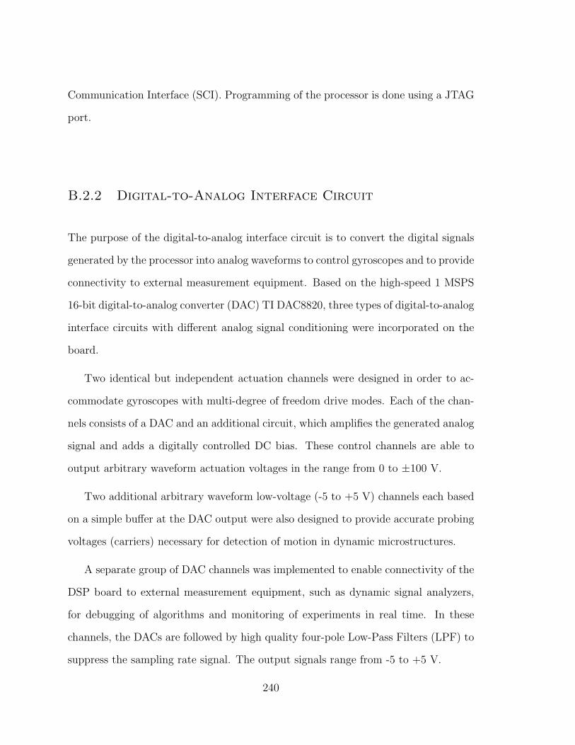
ramped up until self-resonant motion was started, Figure C.4. After the transient
process with characteristic start-up time of 300 ms settled, both the detected veloc-
ity and the feedback generated driving signal were sinusoidal waveforms, Figure C.5.
Spectral measurements of the detected steady state drive-mode velocity were per-
250
Page 25
Self-Resonance: Start-Up
Feedback drive DC+AC
Detected velocity AC
DC is ramped up until self-resonance starts. Time constant is ~300 ms.
Figure C.4: Demonstration of the closed loop self resonance: velocity signal.
formed to analyze the frequency content. As Figure C.6 shows, the self-resonant
motion occurs mostly at the resonant frequency of the mechanical structure. The
measured signal-to-noise ratio was on the order of 50 dB and harmonic distortion
was on the order of 35 dB, demonstrating feasibility of EAM-based velocity feedback
self-resonance.
C.5 Single-Sided and Differential Operation
As mentioned previously, the reported circuit was designed and demonstrated with
both driving and detection signals operated in a differential manner. Differential
operation is an important practical technique for improvement of the signal-to-noise
ratio and dynamic range by the means of common mode parasitics suppression. Fig-
251
Page 26
Self-Resonance: Signals
DC+AC drive Detected velocity
Figure C.5: Demonstration of the closed loop self resonance: drive.
Self-Resonance: Frequency Spectrum
35 d
B
Figure C.6: Demonstration of the closed loop self resonance: spectrum.
252
Page 27
0 10 20 30 40 50 60 70 80 90−110
−100
−90
−80
−70
−60
−50
−40
−30
−20
Frequency, kHz
Mag
, dbV
rms
1−DRV, 1−SNS
(a) Single-sided drive, single-sided pick-up.
0 10 20 30 40 50 60 70 80 90−110
−100
−90
−80
−70
−60
−50
−40
−30
−20
Frequency, kHz
Mag
, dbV
rms
1−DRV, 1−SNS2−DRV, 1−SNS
(b) Differential drive, single-sided pick-up.
0 10 20 30 40 50 60 70 80 90−110
−100
−90
−80
−70
−60
−50
−40
−30
−20
Frequency, kHz
Mag
, dbV
rms
1−DRV, 1−SNS2−DRV, 1−SNS2−DRV, 2−SNS
(c) Differential drive, Differential pick-up.
0 10 20 30 40 50 60 70 80 90−110
−100
−90
−80
−70
−60
−50
−40
−30
−20
Frequency, kHz
Mag
, dbV
rms
1−DRV, 1−SNS2−DRV, 1−SNS2−DRV, 2−SNS2−D&2−S, HPF
(d) Differential drive and pick-up, after LPF.
Figure C.7: Comparison of measured frequency spectrums for single-sided and differ-ential actuation and detection.
ure C.7 illustrates the advantages of differential operation with experimental spectral
measurements of the velocity pick-up signal.
253
Page 29
Appendix D
Allan Variance Analysis
This chapter discusses methods of random process analysis using Allan variance.
While this dissertation is primarily concerned with analysis of random noise compo-
nents in the output signal of a vibratory MEMS gyroscopes, most of the discussed
techniques are equally applicable to analysis of any other random signals.
D.1 Allan Variance Analysis Procedure
A basic procedure of the Allan variance (AVAR) analysis of a signal is presented in
Figure D.1. Allan variance analysis consists of computing a signal’s w(t) root Allan
variance (R-AVAR or RAVAR) σ for different integration time constants τ and then
analyzing the characteristic regions and log-log scale slopes of the σ(τ) curve in order
to identify different noise modes, i.e., random components of the signal with different
autocorrelation power laws σ(τ) ∝ τβ.
The first step of the analysis is to acquire a time history w(t), 0 ≤ t ≤ T , of the
signal of interest using an experimental setup with a digital to analog converter (or
a computer simulation of the experiment). The second step is to fix the integration
time constant τ , divide the acquired time history of the signal into K “bins” of
span τ , average each bin to obtain wk =∫ (k+1)τ
kτw(t)dt, and compute the Allan
255
Page 30
variance defined as one half of the average of the squares of the differences between
the successive averaged values σ2(τ) = 12〈(wk+1 − wk)2〉|k=0...(K−1).
The described sequence of steps yields the estimated value of the root Allan vari-
ance σ(τ) for the chosen integration time constant τ . In order to obtain the whole
σ(τ) curve, the second step is repeated multiple times for a sequence of τ values. Typ-
ically, the integration time constants τ are iterated through the sequence τ = 2n∆T
with n = 0, 1, . . . N , where ∆T is the sampling time of the w(t) time history.
D.2 Random Noise Modes Classification
While an Allan variance curve for a signal contains essentially the same information as
the signal’s power spectral density (PSD), it presents the information in an alternative
and somewhat more convenient way. The power laws of PSD and RAVAR are related
to each other in the following way:
PSD(f) ∝ fα ⇐⇒ σAV AR(τ) ∝ τβ,
where β = −α + 1
2and f = 1/τ.
Figure D.2 presents a classification of main noise components, or modes, based on
their power spectral density and Allan variance power laws. In the following sections
we discuss the three main noise types, i.e, the white, pink or 1/f , and red or 1/f 2
random processes.
256
Page 31
Time
Val
ue
Sample Noise −− Time History
(a) First step: collect a time history w(t) of the signal ofinterest.
Time
Val
ue
Sample Noise −− Time History
log−log AVAR
(b) Second step: divide the time history w(t) into bins ofspan τ and compute σ(τ). Repeat for different times.
Figure D.1: Explanation of Allan variance analysis procedure using an example ran-dom process with a white noise and a random walk components.
SpectralType
PossibleSources
AssociatedTerms
PSD(f)power law
σ(t)power law
LongerAveraging
White ThermalAngle
RandomWalk
f 0 t -1/2
t 0
t -1/2
Pink ElectronicsNoise
Flicker f -1
Good
Neutral
Red(Brown)
White NoiseAccumulation
Angle RateRandom Walk
f -2 Bad
Figure D.2: Classification of random noise modes as applied to rate gyroscopes.
257
Page 32
D.3 White Noise
White noise is a random signal, or process, with a constant power spectral density.
While this definition presents a mathematical abstraction not physically possible due
to its infinite total power, it presents a practically convenient and useful model of
random processes with very short characteristic autocorrelation times. For instance,
the random motion of particles due to mechanical thermal noise has a characteris-
tic cutoff frequency of kBT/h which has a value of approximately 6 THz at room
temperature, making an ideal white noise a good approximation for most practical
purposes.
Important characteristic properties of a white noise type random process in time,
frequency, and Allan variance domains are shown in Figure D.3 using a computer sim-
ulated signal. Power spectral density of the white noise is independent of frequency,
i.e. PSD(f) ∝ fα with α = 0. As expected from Equation E.1, the numerically calcu-
lated root Allan variance of the simulated white noise is governed by σAV AR(τ) ∝ τβ
with β = −1/2, which can be identified from the −1/2 slope of the RAVAR plot in
log-log coordinates.
Figure D.4 illustrates effects of time averaging and integration of a white noise
process. Accumulation or integration of a white noise process yield a random walk
type process whose power spectral density is governed by PSD(f) ∝ fα with α = 2
making it 1/f 2, or equivalently, red noise.
D.4 Pink, 1/f Noise
Random processes with 1/f spectral density power law are naturally the next class
of noise to consider. Flicker noise, commonly encountered in electronic circuits, falls
258
Page 33
0 0.1 0.2 0.3 0.4 0.5 0.6 0.7 0.8 0.9 1−10
−5
0
5
10
Time, s
Val
ue
White Noise (Gaussian)
−2−1
0
Time, s
√AV
AR
√AVAR
0 0.1 0.2 0.3 0.4 0.55
10
15
20
Frequency, HzP
ow/fr
eq, d
B/H
z
Power Spectral Density
Figure D.3: Properties of white noise in time, frequency, and Allan variance domain.
0 10 20 30 40 50 60 70 80 90 100−50
0
50
100
150
200
250
300
Time, s
Val
ue
Averaging and Integration of White Noise
White
Averaged White
Integrated White
Figure D.4: Time averaging and integration of white noise.
259
Page 34
0 0.1 0.2 0.3 0.4 0.5 0.6 0.7 0.8 0.9 1−2
−1
0
1
2
Time, s
Val
uePink "1/f" Noise
−2−1
0
Time, s
√AV
AR
√AVAR
0 0.1 0.2 0.3 0.4 0.5
−20
−10
0
10
20
Frequency, Hz
Pow
/freq
, dB
/Hz
Power Spectral Density
Figure D.5: Properties of pink, 1/f 2 noise in time, frequency, and Allan variancedomain.
into this category. Figure D.5 illustrates time, frequency, and Allan variance domain
properties of 1/f , or pink noise using a computer simulation. A pink noise can be
obtained by low-pass filtering a white noise with a 3 dB per octave filter. Simply
put, pink noise can be differentiated from a white noise process by more visible low
frequency, slow fluctuations. As expected from Equation E.1, RAVAR has essentially
flat profile in the case of pink, or 1/f noise.
D.5 Red, 1/f 2 Noise
The third important type of random noise to consider is red noise characterized by
1/f 2 power spectral density. This type of random process is also often referred to as a
random walk and occurs whenever a white noise is accumulated or integrated. While
not correct from the color spectral parallel, red, or 1/f 2 noise is sometimes referred
260
Page 35
to as Brown noise, in honor of Robert Brown who first studied Brownian motion.
Figure D.6 illustrates time, frequency, and Allan variance domain properties of
random walk, or 1/f 2, process by numerically integrating a computer simulated signal
white noise signal. An alternative way to simulate a random walk process is to low-
pass filter a white noise signal with a 6 dB per octave filter. Random walk signal
shows low frequency, slow fluctuations more pronounced than in the pink, 1/f case.
Since the power spectral density of a random walk is given by PSD(f) ∝ fα with
α = −2, its root Allan variance profile is governed by σAV AR(τ) ∝ τβ with β = −1/2,
which can be identified by the α = +1/2 slope of the RAVAR in the log-log scale.
Figure D.7 illustrates properties of a random walk signal with respect to time
integration and averaging using a computer simulated signal, both of which are detri-
mental to the uncertainty of the produced measurement.
D.6 Random Noise Modes Identification
In the previous sections, we discussed how the characteristic slopes of the root Allan
variance curve can be used to identify random noises of different categories. However,
the true brilliance of Allan variance analysis comes from its ability to easily decouple,
identify, and quantify noise modes with different autocorrelation power laws from a
single, combined random process. Figure D.8 illustrates this concept with a computer
simulated sum of a white and red, or 1/f 2 noises.
As the example shows, it is not straightforward to identify the presence and pa-
rameters of the white and red noise components in the simulated signal from its time
history or power spectral density. At the same time, RAVAR plot of the signal clearly
shows two different regions on the log-log scale plot: a region with the −1/2 slope
corresponding to the white noise component, and a region with a +1/2 slope corre-
261
Page 36
0 0.1 0.2 0.3 0.4 0.5 0.6 0.7 0.8 0.9 1−200
−150
−100
−50
0
50
Time, s
Val
ue
Brown "1/f2" Noise − Integral of White Noise
−20
1
2
Time, s
√AV
AR
√AVAR
0 0.25 0.50
20
40
60
Frequency, Hz
Pow
/freq
, dB
/Hz
Power Spectral Density
WhiteBrown
Figure D.6: Properties of red, 1/f 2 noise in time, frequency, and Allan variancedomain.
0 2 4 6 8 10 12 14 16 18 20−3
−2.5
−2
−1.5
−1
−0.5
0
0.5x 10⁴
Time, s
Val
ue
Averaging and Integration of Brown Noise
BrownAveraged BrownIntegrated Brown
Figure D.7: Time averaging and integration of red, 1/f 2 noise.
262
Page 37
0 0.1 0.2 0.3 0.4 0.5 0.6 0.7 0.8 0.9 1
−100
0
100
200
Time, s
Val
ue
White Noise + Brown Noise
−20
1
Time, s
√AV
AR
√AVAR
0 0.1 0.2 0.3 0.4 0.50
10
20
30
40
50
Frequency, HzP
ow/fr
eq, d
B/H
z
Power Spectral Density
White
White+Brown
Brown
Figure D.8: Identification of noise modes using Allan variance analysis illustratedusing a computer simulated sum of a white noise and a red noise.
sponding to the random walk component. Parameters of the two noise components
can be numerically identified by fitting the two regions of the RAVAR log-log curve
with y = ax−1/2 and y = bx1/2, respectively.
The analysis also allows to identify the crossover time, or frequency, between the
two noise modes. As illustrated in Figure D.8, low-pass and high-pass filtering of the
combined noise with respect to the identified crossover frequency allows to separate
out the two noise components in the time domain.
D.7 Application to Rate Gyroscopes
Root Allan variance analysis of zero rate output of micromachined Coriolis vibratory
gyroscope typically reveals well pronounced white and red noises, 1/f 2 noise modes
(pink, or 1/f noise component is sometimes obscured by the other two noise modes).
263
Page 38
Root Allan variance analysis allows to quantify uncertainty or the rate measurement
as a function of the averaging or integration time in intuitive unit of input angular
rate (usually /s or /h).
One of the traditional applications of gyroscopes is, however, angle measurement.
Since most available micromachined gyroscopes fall into the rate measuring category,
their output has to be integrated to obtain the total angle of rotation. As discussed
in the previous sections, time integration shifts the power spectral density power law
of a random process by −2 exponent. This means that a white noise component in
the rate signal becomes a random walk type component in the angle measurement,
which explains why the white noise of a rate gyroscope is often referred to as angle
random walk (ARW), Figure D.2. Similarly, time integration or a random walk
component of a rate gyroscope output results in a angle measurement noise component
with PSD(f) ∝ fα, α = −4 and root Allan variance σ(τ) ∝ τβ with β = +3/2.
This sheds light on one of the reasons why micromachined rate gyroscopes are not
optimal for applications where an angle measurement is needed. A rate integrating
micromachined gyroscope would provide much better performance since the time
integration of the noise could be avoided.
D.8 Mechanical-Thermal Noise
One of the fundamental performance limits in micromachined vibratory gyroscopes
comes from the mechanical-thermal noise. Analytical investigation of mechanical-
thermal noise output is complicated by the fact that the initial white noise input
first passes through the sense-mode dynamics (which shapes the white noise power
spectral density according to its frequency response profile) and then goes through
the amplitude demodulation with the drive-mode reference signal. Theoretical power
264
Page 39
−1000 −800 −600 −400 −200 0 200 400 600 800 10000
1
2
3
4
5
6
7
Frequency, Hz
Noi
se S
pect
ral D
ensi
ty, [°/h/
√Hz]
Mechanical−Thermal Noise in Mode−Matched MEMS Gyroscopes
linear−log10 scale
√S(ω)=1.5e5√ (KbTω
y/(4Q3A2M) / (ω2+ω
y2/(2Q)2))
Max(√S)=1.5e5√(KbT/(ω
yA2MQ )), FWHP(S)=ω
y/Q
Levered Tuning Fork3×7 mm2×50 µm SOI
2.5 kHz frequency
increasing Q log
10(Q)= 1:0.5:5.5
Figure D.9: Spectral density of mechanical-thermal noise output.
spectral density of mechanical-thermal noise output in Coriolis vibratory microma-
chined gyroscopes is shown in Figure D.9.
Figure D.10 presents a numerical case study of mechanical-thermal noise in MEMS
gyroscopes. A time history of the output obtained using a MATLAB/Simulink model
of a mode-matched Coriolis vibratory gyroscope is shown in Figure D.10(a). Allan
variance curve of the simulated output time history is shown in Figure D.10(b).
Two distinct regions with different slopes can be identified in the Allan variance of
mechanical-thermal noise. At short integration times Allan variance of mechanical-
thermal noise shows a positive slope β due to the low-pass characteristic of the noise
spectral density at long times. At longer integration times, however, the Allan vari-
ance shows a negative slope β due to the fact that the noise spectral density is essen-
tially flat at very slow frequencies. The crossover time between the two regions of the
mechanical-thermal noise Allan variance can be associated with the time constant of
the resonant sense-mode, 1/∆f = Q/f .
265
Page 40
0 10 20 30 40 50 60 70 80 90 100
−3
−2
−1
0
1
2
3
Time, s
Rat
e S
igna
l and
Rat
e N
oise
, °/
h
Mechanical−Thermal Noise in Mode−Matched MEMS Gyroscopes
Output Rate Signal, °/h RMS(Output Rate Signal), °/h Input Rate Signal, °/h
Levered Tuning Fork3×7 mm2×50 µm SOI
2.5 kHz frequency, Q=103
RMS =1.5e5√(KbT/(4A2MQ2)) = 1 °/h
(a) Time history of the input and output.
10−2
10−1
100
101
102
103
104
10−3
10−2
10−1
100
Cluster Time, s
Roo
t Alla
n V
aria
nce,
°/h
Mechanical−Thermal Noise in Mode−Matched MEMS Gyroscopes
Gyroscope output Sense−mode LPF ARW=1.5e5√(KbT/(ω
yA2MQ ))=0.53 °/h
Sense−mode time constant Q/f=0.4 s
Levered Tuning Fork3×7 mm2×50 µm SOI
2.5 kHz frequency, Q=103
(b) Allan variance of the rate output.
Figure D.10: Mechanical-Thermal noise in Coriolis vibratory rate gyroscopes.
266
Page 41
Appendix E
Micro Stage for On-ChipElectro-Mechanical Calibration
This chapter highlights the preliminary development of an on-chip electro-mechanical
self-calibration system for micromachined gyroscopes based on an embedded micro
rotary stage. Figure E.1 illustrates the conceptual design of the system and presents
its potential advantages. The overall goal of the proposed system is the continuous,
in-situ elimination of inertial sensor drifts. The proposed system-on-a-chip utilizes
a Micro Rotary Stage (MiRS) to provide a reference input rate signal, electrical
interconnects to provide uninterrupted power and signal coupling with the rotating
platform, and signal processing algorithm for continuous calibration of scale factor
drifts. The ultimate vision is to combine batch fabricated MiRS with embedded
devices, micro-fluidic interconnects system, and drift elimination electronics to enable
autonomous, drift-free rate sensor system. Alternatively, the MiRS system-on-a-chip
can be used as a versatile packaging platform for separately fabricated microsystems.
E.1 Conceptual Design of the System
The novel drift elimination system based on the MiRS may enable a revolutionary re-
duction of drifts by real-time execution of autonomous, in-situ calibration of sensors.
267
Page 42
Micro Rotary Stage (MiRS) for On-Chip Electro-Mechanical Calibration
Micro Rotary Stages (MiRS) compensates sensor drifts by providing a persistent input reference for continuous recalibration
MiRS for inertial sensors can attain 1000x reduction of scale factor drift
MAIN ACHIEVEMENT:Architecture for system-on-a-chip combining MiRS, inertial sensors, micro-fluidic electrical interconnects system, and signal processing electronics for sensor drift elimination.
HOW IT WORKS: .
KEY INNOVATIONS:• Micro-fluidic electrical interconnects system
with micro-scale carbon electrodes provides uninterrupted transfer of power and signals between the MiRS base and sensor.
• Sensor scale factor is continuously updated using MiRS angular rate reference signal.
• MiRS reference is extremely accurate due to SideBand Ratio (SBR) detection algorithm.
State of the Art (Draper Lab):Precision/ resolution 1 °/hRepeatability 500 °/h
Low repeatability limits potential applications
QU
AN
TIT
AT
IVE
IM
PA
CT
EN
D-O
F-P
RO
JEC
T G
OA
L
ST
AT
US
QU
ON
EW
IN
SIG
HT
S
Stand alone MEMSgyroscope scale factor stability
400ppm
MiRS with embeddedgyroscope scale factor stability
<2ppm
MiRS robustness is enabled by SBR detection with inherent self calibration
Fully integrated MiRS and inertial sensor on a chip with 1000x improved scale factor drift
Figure E.1: Conceptual design and potential advantages of an on-chip electro-mechanical calibration system enabled by an embedded micro rotary stage.
While the MiRS architecture can augment the functionality of various sensors, the
main focus is on the drastic improvement of MEMS gyroscopes drifts. During opera-
tion, the embedded gyroscope is subject to both external input angular rate (DC to
100 Hz frequency range) as well as a persistent, sinusoidal reference generated by the
MiRS at a frequency higher than the gyroscope’s desired bandwidth (on the order of
200 Hz). The gyroscope output will contain signals corresponding to both the exter-
nal rate and the internal reference which can be frequency de-multiplexed into the low
frequency response to the external angular rate, and the higher frequency response to
the MiRS reference. Through continuous measurement of the “Calibration Output”
to the “MiRS Calibration Reference” ratio, the algorithm eliminates scale factor drift
from the final angular rate measurement. The MiRS enabled gyroscope with in-situ
calibration is projected to achieve <2 ppm stability - a 1000 improvement compared
268
Page 43
to the current state of the art.
In order to implement and demonstrate the proposed system, a number of engi-
neering challenges need to be addressed, including the following:
1. Mechanical crosstalk between a MiRS and the embedded sensor. The MiRS
structural modes should be precisely engineered to yield one low-frequency op-
erational mode, while elevating the higher frequency modes away from the sen-
sor’s sensitive frequencies.
2. Electrical contact quality and reliability. Technology for micro-glassblowing
with pre-deposited metal traces can be developed to produce very smooth micro-
channels. The glass-blown micro-channels may enable an intriguing capability
of conductive liquid (liquid metals or ionic fluids) encapsulation. Elimination of
the dry contact by the fluidic electrical interconnects may allow exceptionally
low friction and wear combined with low resistance electrical contact.
The complete micromachined rate table system-on-a-chip consists of three main
components: a Micro Rotary Stage (MiRS) to provide an input reference rate signal
to the gyroscope, micro-fluidic electrical interconnect system for continuous electri-
cal power and signal coupling with the rotating platform, and the drift elimination
algorithm to perform the autonomous, real-time recalibration. Specific technical ap-
proaches for realizing the mechanical structure of the MiRS are discussed in [135].
Below we review a proposed design of the calibration algorithm.
E.2 Scale Factor Drifts in Rate Gyroscopes
The input-output relationship of a sensor, such as a MEMS gyroscope, can be de-
scribed as Vout(Ωin) = SF [G] × Ωin, where Ωin is the input angular rate, Vout is the
269
Page 44
SBRDetector
Control
Feedb
ack
||||Calibration Output
Micro-Rotary Stage (MiRS)with embedded MEMS gyroscope
Self-CalibrationAlgorithm
MiRS Calibration Reference
Input RateUncalibrated Output
In-SituCalibratedRateOutput
||||||||
(2)(1)x( / )(3)
(3)
(1)
(2)
LPF
HPF
V (Ù )out in
Total Gyro Output
Ùin
Ùref
Figure E.2: MiRS based in-situ calibration algorithm for real-time drift elimination.
output voltage, and SF [G] is the gyroscope’s scale factor. Generally, the scale factor
value is identified through initial calibration and ideally remains constant through the
lifetime of the sensor. However, a more realistic model that reflects experimentally
observed drifts is given by
SF [G] = SF0[G] + SF∆[G] + SFσ[G], (E.1)
where SF0[G] is the nominal constant value, SF∆[G] is a slowly varying drift com-
ponent responsible for loss of calibration and decreased accuracy, and SFσ[G] is a
stochastic component of the gyroscope’s instantaneous scale factor with standard de-
viation σ. Periodic calibration is needed to eliminate SF∆[G] and minimize the effect
of SFσ[G]. MEMS gyroscope scale factor drifts are extremely challenging to com-
pensate due to complex dynamics of the multi degree of freedom electromechanical
system with multiple drift-prone parameters and extremely small Coriolis-induced
sense-mode displacements.
270
Page 45
E.3 Proposed Calibration Algorithm
In the proposed rate measurement system, Figure E.2, a self-calibration algorithm is
employed to produce a final, drift-free, voltage output proportional to the external
input angular rate. The idea of the algorithm is to use the continuously measured
ratio between the “Calibration Output” and “MiRS Output Calibration Reference”
to cancel out any drifts of the MEMS gyroscope. More specifically, the input-output
relationship for the proposed rate measurement system can be derived as
Vout(Ωin) = SF [G]× Ωin ×SF [MiRS]× γ0
SF [G]× γ0
= SF [MiRS]× Ωin, (E.2)
where SF [MiRS] is the scale factor of the integrated MiRS and γ0 is the amplitude
of the generated sinusoidal angular rate reference signal. The scale factor of the
proposed system does not depend on the scale factor (and its drift) of the embedded
gyroscope; instead, it is defined only by MiRS scale factor SF [MiRS].
The proposed MiRS is a single degree of freedom system operated in continuous,
large amplitude self-resonant motion. As shown in Figure E.3, these unique char-
acteristics of the MiRS allows the direct application of the SideBand Ratio (SBR)
detection method described in [123, 132]. The SBR detection method constructively
utilizes the inherent nonlinearity of parallel plate capacitive pick-up and is robust to
variations of critical parameters: nominal capacitance, frequency and amplitude of
the probing voltage, and amplifier gain. Robustness of the SBR detection method
untimely translates into extreme stability of the MiRS scale factor and consequently
can provide a 3 order of magnitude improvement to the stability and drift of the
proposed rate system with on-chip autonomous self-calibration.
271
Page 46
amplitude of motion x0is detected independently of
R, Csn, ωc, and vcwhile also boosting the SNR.
SBR r
)(tCplates)sin()( 0 txtx dω=
)sin( tvV ccdc ω+ Current
SBR r
γ
x0=2r/(r2+1)
Figure E.3: SideBand Ratio (SBR) detection of motion constructively utilizes nonlin-earity of capacitive pick-up to provide the MiRS with superior robustness and scalefactor stability.
272