Appendix A: Logic Symbols Internationally accepted symbols allow us to represent circuits of different levels of complexity in terms which are readily understood irrespective of the reader's everyday language. Many different levels are needed to cater for the wide range of possible uses, but Kampel (Kampel, 1985) has suggested three main divisions. The flrst is systems level engineering, requiring pure symbolic logic or conceptual diagrams, describing the system only in block schematic form. The second divi- sion is design engineering, in which we are concerned with subsystem inter- connections but without defming the precise method of implementation. This requires functional block diagrams. Thirdly we have component level engineering, which is concerned with the physical interconnection of devices, requiring a detailed circuit diagram including pin numbers, device types and positions on a printed circuit board layout, connector details and so on. Earlier standards have been limited to gate symbols which have been useful only at the third level, and higher levels of abstraction have been prepared, in general, in the form of large block diagrams containing a fair amount of detailed textual description. The most popular example of this gate level type of standard is the American Mil. Spec. Standard, ANSI Y32-14-1973, in which the shape of the symbol denotes the logical operation involved and, in common with most textbooks, we use this standard for its simplicity. More modern methods have replaced Y32-14 with regular rectangular symbols which are more easily drawn on automatic drafting equipment, but there is still a direct equivalence as shown in flgure A.l. The most recent standard, published by the International Electrotechnic Commission in 1983 as IEC Pub. 617-12, 1983, goes beyond simple gate symbols, and allows meaningful symbols to be developed for even very complex circuits, such as Vl.SI devices, by the use of symbols embedded within symbols and a powerful dependency notation. Many national standards organizations have accepted the IEC standard and have published their own versions. In the UK it is known as British Standard BS3939: section 21, and in the USA as ANSI/IEEE Std 91-1984. 284
Transcript
Appendix A: Logic Symbols
Internationally accepted symbols allow us to represent circuits of different levels of complexity in terms which are readily understood irrespective of the reader's everyday language. Many different levels are needed to cater for the wide range of possible uses, but Kampel (Kampel, 1985) has suggested three main divisions. The flrst is systems level engineering, requiring pure symbolic logic or conceptual diagrams, describing the system only in block schematic form. The second division is design engineering, in which we are concerned with subsystem interconnections but without defming the precise method of implementation. This requires functional block diagrams. Thirdly we have component level engineering, which is concerned with the physical interconnection of devices, requiring a detailed circuit diagram including pin numbers, device types and positions on a printed circuit board layout, connector details and so on.
Earlier standards have been limited to gate symbols which have been useful only at the third level, and higher levels of abstraction have been prepared, in general, in the form of large block diagrams containing a fair amount of detailed textual description. The most popular example of this gate level type of standard is the American Mil. Spec. Standard, ANSI Y32-14-1973, in which the shape of the symbol denotes the logical operation involved and, in common with most textbooks, we use this standard for its simplicity. More modern methods have replaced Y32-14 with regular rectangular symbols which are more easily drawn on automatic drafting equipment, but there is still a direct equivalence as shown in flgure A.l.
The most recent standard, published by the International Electrotechnic Commission in 1983 as IEC Pub. 617-12, 1983, goes beyond simple gate symbols, and allows meaningful symbols to be developed for even very complex circuits, such as Vl.SI devices, by the use of symbols embedded within symbols and a powerful dependency notation. Many national standards organizations have accepted the IEC standard and have published their own versions. In the UK it is known as British Standard BS3939: section 21, and in the USA as ANSI/IEEE Std 91-1984.
284
APPENDIX A 285
IEC617-12 ANSI Y32-14 AND
~=B-f ~D-f f =ABC
OR
~D-f A=EJ-- f=A+B+C 8 f c
NAND
~o-f Afi- f=ABC B f c
NOR
~=[)o-f AD- f=A+B+C 8 " f c
Inverter
A{}-f A --[>o-f f=A
Exclusive-OR
:=E}-f :=JD-f f=A®B
Flipflop Preset Preset
Data Data
Ciock Clock
Figure A.l
A.1 An introduction to graphical symbols for diagrams: binary logic elements (IEC Pub. 617-12, 1983)
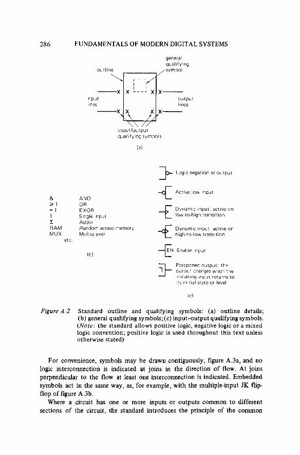
The outline of each symbol is rectangular, but the height.to-width ratio is not defmed. A general qualifying symbol is placed centrally at the top of the outline to indicate the logic function. The logic flow in a diagram is conventionally from left to right, and, where appropriate, from top to bottom. Thus, in general, inputs should be shown on the left of the symbol and outputs on the right. Where a flow contrary to the conventional is necessary, arrowheads can be included on interconnecting lines to ensure clarity. Additional qualifying symbols relating to individual input and output connections are positioned at the input or output involved, adjacent to the outline. The more common general qualifying symbols and input-output qualifying symbols are shown in figure A.2.
286 FUNDAMENTALS OF MODERN DIGITAL SYSTEMS
& ;;;>1 = 1 1 ~ RAM MUX
etc.
outline
input lines
input/output qualifying symbols
(a)
general qualifying symbol
output lines
J Logic negation at output
AND OR EXOR Single tnput Adder Random access memory Multiplexer
(b)
Active low input
Dynam1c input active on low-to-high transition
Dynamic input· active on high-to-low transition
~ Enable input
Postponed output the output changes when the in1t1at1ng input returns to 1ts tn1tial state or level
(c)
Figure A.2 Standard outline and qualifying symbols: (a) outline details; (b) general qualifying symbols;(c) input-output qualifying symbols. (Note: the standard allows positive logic, negative logic or a mixed logic convention; positive logic is used throughout this text unless otherwise stated)
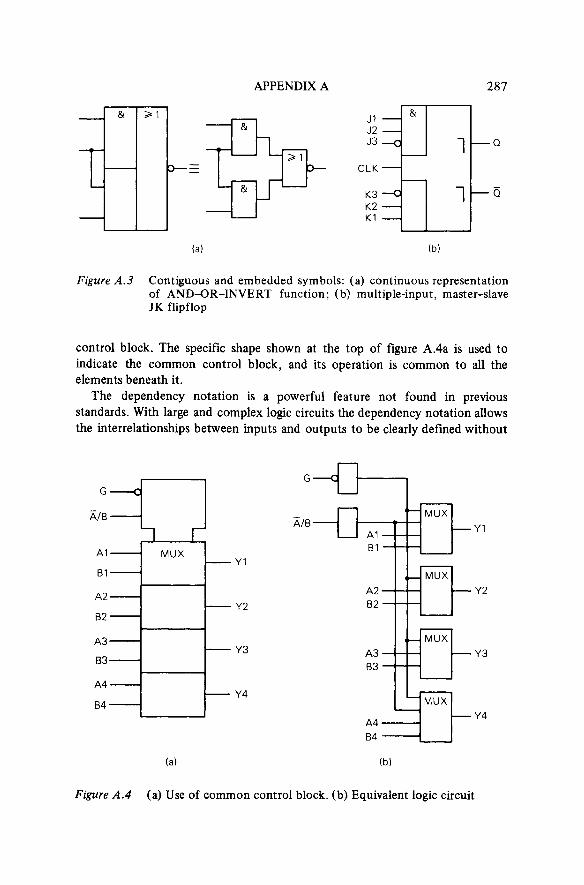
For convenience, symbols may be drawn contiguously, figure A.3a, and no logic interconnection is indicated at joins in the direction of flow. At joins perpendicular to the flow at least one interconnection is indicated. Embedded symbols act in the same way, as, for example, with the multiple-input JK flipflop of figure A.3b.
Where a circuit has one or more inputs or outputs common to different sections of the circuit, the standard introduces the principle of the common
APPENDIX A 287
;;;.1 J1 J2 J3 l Q
CLK
K3 l 6 K2 K1
(a) (b)
Figure A.J Contiguous and embedded symbols: (a) continuous representation of AND-OR-INVERT function; (b) multiple-input, master-slave JK flipflop
control block. The specific shape shown at the top of figure A.4a is used to indicate the common control block, and its operation is common to all the elements beneath it.
The dependency notation is a powerful feature not found in previous standards. With large and complex logic circuits the dependency notation allows the interrelationships between inputs and outputs to be clearly defmed without
G G
A/8 A/8 Y1
A1 Y1
81
A2 Y2 Y2
82
A3 Y3 Y3
B3
A4 Y4
84 Y4
(a) (b)
Figure A.4 (a) Use of common control block. (b) Equivalent logic circuit
288 FUNDAMENTALS OF MODERN DIGITAL SYSTEMS
having to show how they are actually achieved. The principle is simple enough: any input or output affecting other inputs or outputs is labelled with a letter and an identifying number. Any input or output affected by that input or output is labelled with the same number. Certain letters have been reserved for specific relationships; G, for example, indicates an AND relationship and V indicates an OR relationship. The AND-OR-INVERT gate symbol of figure A.3 can now be simplified to the form shown in figure A.5. It should be remembered, of course, that the whole aim of a logic diagram is to present the information as clearly as possible, and the dependency notation is not necessary for straightforward gate interconnections and similar low levels of complexity.
A ;;.1
A
B
becomes B Gl
c c
Figure A.5 The dependency notation used in the AND-OR-INVERT function
References
Kampel, I. (1985). A Practical Introduction to the New Logic Symbols, Butterworth, London
Mann, F. A. (1985). An explanation of logic symbols- Overview of IEEE Standard 91-1984, in The TTL Data Book, Vol. 1, Texas Instruments
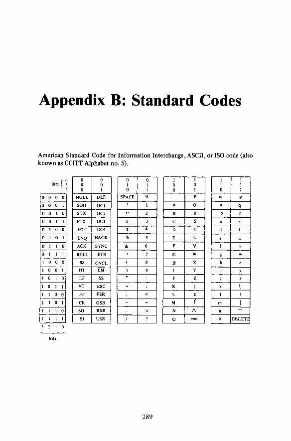
Appendix B: Standard Codes
American Standard Code for Information Interchange, ASCII, or ISO code (also known as CCITT Alphabet no. 5).
0 0 0 0
0 0 0 I
0 0 I 0
0 0 I I
0 I 0 0
0 I 0 I
0 I I 0
0 I I I
I 0 0 0
I 0 0 I
I 0 I 0
I 0 I I
I I 0 0
I I 0 I
I I I 0
I I I I
1 2 I 0
'-----' Bits
0 0 0 0 0 I
NULL OLE
SOH DCI STX DC2
ETX DC3
EOT DC4
ENQ NACK
ACK SYNC
BELL ETB
BS CNCL HT EM
LF ss VT ESC
FF FSR
CR GSR
so RSR
Sl USR
0 0 I I I I I I 0 0 I I 0 I 0 I 0 I
SPACE 0 p @ p
! I A Q a q
" 2 B R b r
# 3 c s c s
s 4 D T d t
% 5 E u e u
& 6 F v f v
' 7 G w g w
( 8 H X h X
) 9 I y i y . : J z j z
+ ; K [ k {
< L f. I I
- = M 1 m }
> N (\ n -,
I ? 0 -- 0 DELETI
289
Ext
ende
d bi
nary
-cod
ed-d
ecim
al i
nter
chan
ge c
ode,
EB
CD
IC
{ 7
lo
Bit
s ~
I o
I o
I o
I 0
I 0
1 1
0 0
0 1
0 0
0 0
0 0
I 1
0 I
0 1
0 u
0 0
Nl'
LL
D
S SP
AC
E
&
0 0
0 1
SST
0 0
1 0
FDS
0 0
1 1
TM
lo 1
0 0
PF
RE
S B
YP
PN
lo 1
0 1
HT
NL
L
F R
ST
0 1
1 0
LC
BS
EOB
uc
0
1 1
1 D
EL
ET
E
IL
PR
EOT
1 0
0 0
DL
E
CN
CL
1 0
(l
I SO
H
DC
I EM
1 0
I 0
STX
D
C2
SM
ss
£ !
----
1 0
1 I
ET
X
DC
3 V
T
ESC
s
1 1
0 0
DC
4 F
F
FSR
<
.
----
1 1
0 1
EN
Q
NA
CK
C
R
GSR
(
)
1 1
1 0
AC
K
SYN
C
so
RSR
I
+
1 I
1 1
BE
Ll
ET
B
Sl
l'SR
I
I I
3 I 2
j11 o
-------
Bits
Con
trol
cha
ract
er a
bbre
viat
ions
: A
CK
A
ckno
wle
dge
ET
X
End
of
text
B
EL
L
Aud
ible
sig
nal
FDS
Fie
ld s
epar
ator
BS
B
acks
pace
F
F
For
m f
eed
BY
P B
ypas
s FS
R
Fil
e se
para
tor
CN
CL
C
ance
l G
SR
Gro
up s
epar
ator
C
R
Car
riag
e re
turn
H
T H
oriz
onta
l ta
bula
tion
D
C
Dev
ice
cont
rol
lL
Idle
D
LE
D
ata
line
esca
pe
LC
Low
er c
ase
DS
Dig
it s
elec
t L
F L
ine
feed
EM
E
nd o
f m
ediu
m
NA
CK
N
egat
ive
ackn
owle
dge
EN
Q
En
qu
iry
N
L
New
lin
e EO
B
End
of
bloc
k N
UL
L
All
zero
E
OT
E
nd o
f tr
ansm
issi
on
PF
Pun
ch o
ff
ESC
E
scap
e PN
P
unch
on
ET
B
End
of
tran
smis
sion
blo
ck
PR
Pref
ix
I 0
I 0
1 I
1 1
0 0
1 1
0 0
0 1
0 1
.......
I a
j
b k
c I
d m
e n
f 0
-· g
p
h q
i r
1\
#
%
@'
- >
=
' ..
__ _:_
___
-
RE~
Res
tore
R
SR
Rec
ord
sepa
rato
r R
ST
R
eade
r st
op
Sl
S
hift
in
SM
Set
rno
de
so
Shi
ft o
ut
SOH
S
tart
of
head
ing
ss
Sta
rt o
f sp
ecia
l 5e
quen
ce
SST
Sig
nifi
canc
e st
arte
r ST
X
Sta
rt o
f te
xt
SYN
C
Syn
chro
nous
idl
e TM
T
ape
mar
k uc
U
pper
cas
e U
SR
Uni
t se
para
tor
VT
V
erti
cal
tabu
lati
on
1 1
0 0
1 1
0 I
' I u v w
X y z
~-~
! I
! ~
I ~
! I
I I
I 0
0 I
I 0
I 0
1 0
A
J I
B
K
s l
c L
T
3
D
M
u 4
E
N
v 5
F 0
w
6
G
p X
7
H
Q
y 8
I R
z
9
ER
RO
R
N
\0
0 ~ ~ m
z ~ f;; 0 '"I1 ::: 0 0 m
~ 0 6 ~ >
t""'
(/) ~ >-i ~ (/)
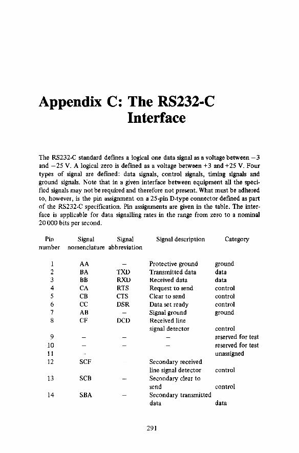
Appendix C: The RS232-C Interface
The RS232-C standard defines a logical one data signal as a voltage between -3 and -25 V. A logical zero is defined as a voltage between +3 and +25 V. Four types of signal are defined: data signals, control signals, timing signals and ground signals. Note that in a given interface between equipment all the specified signals may not be required and therefore not present. What must be adhered to, however, is the pin assignment on a 25-pin D-type connector defmed as part of the RS232-C specification. Pin assignments are given in the table. The interface is applicable for data signalling rates in the range from zero to a nominal 20 000 bits per second.
Pin Signal Signal Signal description Category number nomenclature abbreviation
1 AA Protective ground ground 2 BA TXD Transmitted data data 3 BB RXD Received data data 4 CA RTS Request to send control 5 CB CTS Clear to send control 6 cc DSR Data set ready control 7 AB Signal ground ground 8 CF DCD Received line
signal detector control 9 reserved for test
10 reserved for test 11 unassigned 12 SCF Secondary received
line signal detector control 13 SCB Secondary clear to
send control 14 SBA Secondary transmitted
data data
291
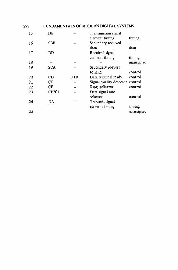
292 FUNDAMENTALS OF MODERN DIGITAL SYSTEMS
15 DB Transmission signal element timing timing
16 SBB Secondary received data data
17 DD Received signal element timing timing
18 unassigned 19 SCA Secondary request
to send control 20 CD DTR Data terminal ready control 21 CG Signal quality detector control 22 CE Ring indicator control 23 CH/CI Data signal rate
(b)T =(A+ B + c +D) (A+ B + C +D) (A+ B + c +D) (A+ B + C +D) (A + B + C + D) (A + B + C + D) (A + B + C + D).
1.4 Mrs Smith went to the Ministry of Secrets. 1.5 f = (AB + AB)(A +D). 1.6 (A+ B)(B + D)(A + c +D). 1.7 f= (A+ B)(A +C); f= A+ BC. 1.8 The set of prime implicants is (BC) (ABD) (ABC) (ACD) (BCD). 1.9 The function is fully symmetric. 1.10 Non-equivalence symmetry in AB and equivalence symmetry in BC and
(b1) S~(ABCDE) (b2) stz ( cl) f = ABC ( c2) f = A + B + C ( c3) f = A (!) B (!) C
1.13 The circuit must generate a function such as f= (A+ B) (CD+ CE +DE)+ CDE + AB(C + D +E).
1.15 X= AD(B +C)+ ABC+ BCD; Y =AD+ BC +BCD; Z = BC + BD +BCD.
1.16 f= (A+ 8 + D)C.
Chapter2
2.1 (a) 13.375 2.2 (a) 653.715 2.3 (i) 0001011
(b) 38.3125 (c) 427.328125. (b) 427.900390625. (ii) 1111011 ( -0000101).
293
294 FUNDAMENTALS OF MODERN DIGITAL SYSTEMS
Chapter 3
3.1 (i) NM 1 = 1.0 V (ii) Nl0 = 0.6 Nl 1 = 0.4.
Chapter 5
5.3 The output code sequence is 0, 1, 2, 3, 4, 8, 9, 10, 11, 12. 5.5 A 3-input AND gate is used to recognize the 000~ condition and to
inject a zero via the 3-input exclusive-OR gate. The sequence is then 0101100100001111
Chapter 6
6.3 The're are essential hazards when in state A with inputs 11 and in state C with inputs 00. They are not critical because of the full address decoding used in the ROM.
6.4 The K input of the fourth stage is stuck at '1 '. The most likely single fault is a solder short to+ 5 V on the printed circuit board.
SOLUTIONS TO SELECTED PROBLEMS 295 6.10 Reset Internal Input Next Output
9.3 (a) Each character has 11 bits giving 110 bits/s. B ;;> 110/2 =55 Hz. (b) Baud rate oliO; 2 x 4.8 x 103 = 9600 baud.
(i) Each character has 10 bits, giving 960 characters per second. (ii) 1000 bytes require 8016 bits, giving a transfer rate of
9600 x 1000/8016, that is 1197 characters per second. 9.4 Each character has 11 bits, so time per character is 11/9600 = 1.15 ms.
The fmal data bit is latched approximately midway through the ninth bit period of the character, and is followed by the parity and stop bit periods. The time available without double-buffering is, therefore, approximately 2.5 bit periods, or 2.5/9.6 ms; that is 0.26 ms.
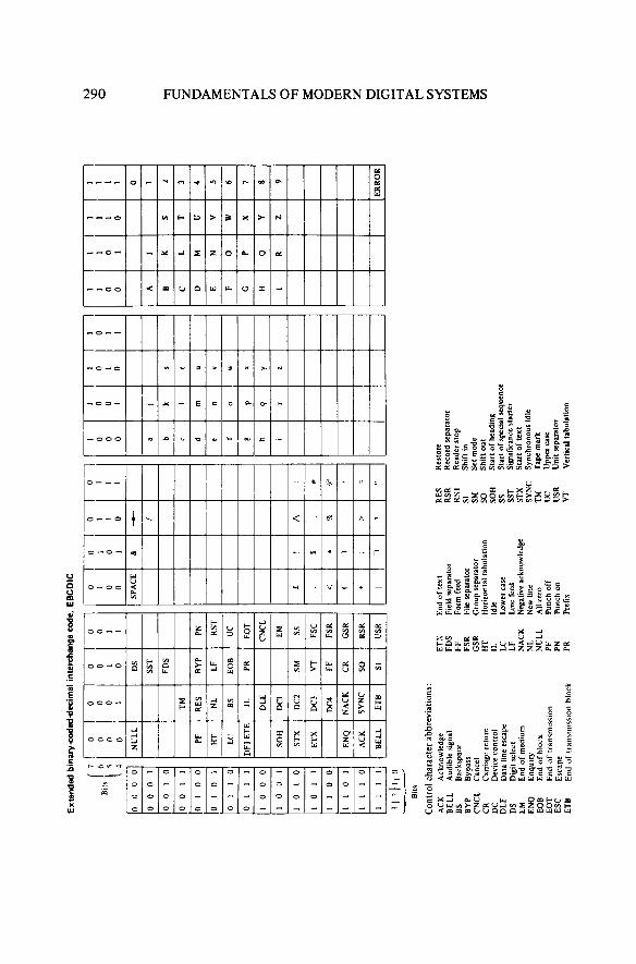
Babbage, C. 78 Bar code 70 Base 44 Base address 253 Base conversion 47-50 Baud rate 281 BCD, binary coded decimal 63-6 Bias, in floating point number 57 Binary arithmetic 52-8 Binary coded decimal, BCD 63-6 Binary counter 151 Bit 45 Bit organized memory 200 Bit search technique 217 Bit-slice device 25 9 Block parity 69 Boole, G. 1 Boolean difference 130 Bottoming, of transistor 80 Boundary condition 137 Branch instruction 238 Broadcast network 270 BS3939 standard 284 Bubble memory device, BMD 212 Buffered CMOS 94 Bus transfers 234 Byte-wide memory 204
Call instruction 238 Cambridge ring 270 Canonical form 12 Canonical term 13 Carry 58 Carry flag 241 Carry look -ahead adder 61 CD-ROM 199 Channel 82 Characteristic, in floating point
number 55
297
298
Charge storage 81 Charge-coupled device, CCD 216 Chip select 204 Clamping diode 80 Class, of sets 2 Clock signal 142 Clocktime 245 CMOS 92 Combinationallogic 2 Commutative laws 6 Compare instruction 244 Compatability, of states 172 Complement
diminished radix 52 radix 51
Complementary MOS logic, CMOS Complementary set 6 Composite state table 170 Condition flags 241 Conditional output box 186 Connectives AND, OR 6 Content addressed memory, CAM
199,217 Control bus 234 Control unit, of microcomputer
245-55 Controlled gate 227 Correction factor, in BCD addition
64 Counter 150-6
binary 151 decade 152 Johnson 154 programmable 155 ring 155 ripple 150 synchronous 15 1 twisted ring 154
Creeping code 68, 15 4 Critical race 1 04 Crosstalk 98 Crystal-controlled oscillator 15 6 Current hogging 86 Current loop, 20 rnA 267 Current page addressing 250 Current pulse encoding 221 Custom IC design 126-8 Cycle time 203
INDEX
Daisy chain interrupt 258 Data bus 234 Data direction register, DDR 232 De Morgan's laws 8, 36 Decade counter 152 Decimal adjust instruction 242 Decimal notation 44 Decision box 186 Decoding matrix 113 Decrement instruction 244 Delay element 189 Delay modulation 222 Delayed outputs 186 Demultiplexing 264 Depletion MOS transistor 82
End around carry 54 Enhancement MOS transistor 82 Equivalence symmetry 17 Equivalent states 172 Erasable PROM 209 Error detection 69 Error-checking code 149 Essential hazard 185 Essential prime implicants 29 Ethernet 272 Even parity 69 Excess-three code 65 Excitation equations 160 Excitation table 161 Exclusive-OR 23, 58, 76,227,240 Execute cycle 230 Exponent, in floating point number
55 Extended BCD interchange code,
EBCDIC 73, 290 Extended direct address 249
Factorization 31 Fall time 81 F AMOS device 211 Fan in 91 Fan out 87 Feedback shift register 146 Ferrite core store 199 Fetch cycle 230 Fibres, optical 267 Field, of instruction 248 Field programmable logic array, FPLA
Floating gate transistor 211 Floating point number 55 Floppydisc 218 Flow diagram 138
Flow matrix 137 Flying head 218 Fraction, in floating point number 55 Frame 263 Frequency modulation 222 Full adder 58 Full custom design 128 Full duplex operation 262 Full subtractor Ill Fundamental mode operation 164 Fusible link PROM 210
Gate, in MOS transistor 82 Gate, logic 18 Gate array design 126 Gate symbols 19, 89 Generate function in adder 61 Generator polynomial 274 Glitch 105 Gray code 67, 7 6 Ground plane 91 Grouping
of ones 25 of zeros 29 using variable-entered map 29
Half adder 24, 58 Half carry flag 241 Half duplex operation 262 Hamming distance 150 Handshaking technique 269 Hard sectoring, of floppy disc 21 9 Hazard
dynamic 104 essential 185 static 104
Hexadecimal system 45 High level data link control, HDLC
273 Highway 262 HP-IB standard 268 Huntington, E. V. 1 Hysteresis, in Schmitt trigger 101
Idling condition 264 IEC617-12st&ndard 284 IEC 625 standard 268 IEEE 488 standard 268 IEEE 696 standard 268 IEEE 802 standard 271-3 Immediate operand 249 Immediate outputs 186
300 INDEX
Implication chart 17 5 Implied address 249 Increment instruction 244 Index register 253 Indexed address 252 Indirect address 252 Inherent address 249 Input protection, of MOS circuits
94 Input/output port 231 Instruction 229 Instruction cycle 231 Instruction register 237 Instruction set 235 Integrated circuit 84 Integrated injection logic, I2 L 89 Integrated Schottky logic, ISL 89 Interface 262 Interfacing, of logic families 106 Internal state 160 Internal state circuit 166 International Article Numbering
Association 70 Interrupt control unit 255-9 Interrupt enable flag 241 Interrupt mask 256 Interrupt routine 256 Intersection, of sets 3 Inverse Karnaugh map 35, 109 Inversion, logical 6, 240 Inversion layer 83 Inverter 18 ISO code 73 Iterative arrays 13 5-9
JK flipflop 143 Johnson code 154 Jump instruction 238 Jump to subroutine 238 Junction capacitance 79
NAND function 36 NAND transform 35 Negative flag 241 Negative logic convention 85 Negative numbers 51
sign plus magnitude 52 Nesting memory 257 Next state variable 161 Nibble 244 Nine's complement 52 NMOS 82 Noise immunity 99 Noise margin 98 Noise sensitivity 99 Non-critical race 104 Non-equivalence symmetry 17 Non-return to zero encoding, NRZ
221 NOR function 36 NOR transform 35 Not equivalence gate 23, 58, 76 NOT function 6 NRZl encoding 222 Null set 6 Number range 55 Number systems 44-7 Nybble 244
verter 277 Sum of products 12 Super large scale integration, SLSI 84 Switch debouncing 142 Switching times 81 Symbols, logic 19, 284 Symmetric functions 17 Synchronous counter 151 Synchronous data link control, SDLC
V .24 standard 268 Variable entered map, VEM 11 Variables of symmetry 17 Vector, in interative arrays 13 5 Vectored interrupt 258 Veitch diagram 2 VEM, variable entered map 11 Venn diagram 2 Vertical MOS transistor 83 Very large scale integration, VLSI 84 VLSI design 97 VMOS transistor 83 Volatile memory 201
Weightings, in positional notation 44 Williams' tube store 199 Winchester technology 219 Wire-OR logic 89, 94, 108, 270 Word length 55 Word line 201 Word organized memory 200 Working register 233 Workspace pointer, WP 234