IntroductionThe LM5071 evaluation board is designed to provide a lowcost, fully IEEE 802.3af compliant Power over Ethernet(PoE) power supply, capable of operating with both PoE andauxiliary (AUX) power sources. The evaluation board fea-tures the LM5071 PoE Powered Device (PD) interface andcontroller integrated circuit (IC) configured in the versatileflyback topology.
Features of the LM5071 EvaluationBoard:• Single Isolated 3.3V output
• Dual Isolated 5V and 3.3V outputs supported (see Figure12)
• Maximum output current 3.3A
• Input voltage range (full power):
With the installed wide-voltage-range EP13 transformer
PoE input voltage range: 38 to 60V
AUX input voltage range: 14 to 60V
With the optional, efficiency-optimized EP13 trans-former
PoE input voltage range: 38 to 60V
AUX input voltage range: 24 to 60V
• Measured maximum efficiency:
With the installed wide-voltage-range EP13 transformer
DC to DC converter efficiency: 81% at 3A
Overall efficiency (including diode bridge): 78.5% at 3A
With the optional, efficiency-optimized EP13 trans-
former
DC to DC converter efficiency: 84% at 3A
Overall efficiency (including diode bridge): 81.5% at 3A
This application note focuses on the evaluation board.Please refer to the datasheet for detailed information aboutthe complete functions and features of the LM5071 IC.
A Note about Input PotentialsThe LM5071 is designed for PoE applications that are typi-cally -48V systems, in which the notations GND and -48Vnormally refer to the high and low input potentials, respec-tively. However, for easy readability, the LM5071 datasheetwas written in the positive voltage convention with positiveinput potentials referenced to the VEE pin of the LM5071.Therefore, when testing the evaluation board with a benchpower supply, the negative terminal of the power supply isequivalent to the PoE system’s -48V potential, and the posi-tive terminal is equivalent to the PoE system ground. Toprevent confusion between the datasheet and this applica-tion note, the same positive voltage convention is usedherein.
Schematic of the Evaluation BoardFigure 1 shows the schematic of the LM5071 evaluationboard. See the Appendix for the Bill of Materials (BOM).
National SemiconductorApplication Note 1430Youhao XiApril 2006
Figure 2 shows the connections for the LM5071 evaluationboard.
The LM5071 evaluation board has three ports for connec-tions. The RJ45 receptacle connector is for PoE input, thePJ102A power jack for AUX input (also accessible with postsP3 and P4 located right behind the jack), and the 3.3V outputport accessible with posts J4 and J5.
For the PoE input, two diode bridges BR1 and BR2 steer thecurrent to the positive and negative supply pins of theLM5071. For the AUX input, the high potential of the AUXinput voltage should feed into the center pin of the PJ102Ajack.
For the output connection, the load can be either a passiveresistor or active electronic load. Attention should be paid tothe output polarity when connecting an electronic load. Useof additional filter capacitors greater than 20 µF total acrossthe output port is not recommended unless the feedbackloop compensation is adjusted accordingly.
Sufficiently large wire size not smaller than AWG #18 isrequired when connecting the source supply and load. Also,monitor the current into and out of the unit under test.Monitor the voltages directly at the board terminals, as re-sistive voltage drops along the connecting wires may de-crease measurement accuracy. Never rely on the lab supplyvoltmeter if accurate efficiency measurements are needed.
When measuring the dc-dc converter efficiency, the con-verter input voltage should be measured across C4 or C5, asthis is the input of the converter stage. When measuring theevaluation board overall efficiency, both input and outputvoltage should be read from the terminals of the evaluationboard.
Source PowerTo fully test the LM5071 evaluation board, a DC powersupply capable of at least 60V and 1A is required for the PoEinput. For the AUX source power, use a DC power supplycapable of 1.5A. Use the output over-voltage and over-current limit features of the bench power supplies to protectthe board against damage by errant connections.
Loading / Current LimitingBehaviorA resistive load is optimal, but an appropriate electronic loadspecified for operation down to 2.0V is acceptable. Themaximum load current is 3.3A. Exceeding this current at lowinput voltage may cause oscillatory behavior as the part willgo into current limit mode. Current limit mode is triggeredwhenever the current through the PoE connector exceeds390mA (nominal). If current limit is triggered, the switchingregulator is automatically disabled by discharging the soft-start capacitor C26 through the SS pin. The module is thenallowed to restart, but the unit will operate in an automaticre-try (hiccup) mode as long as the over-current conditionremains.
Power UpIt is suggested to apply PoE power first. During the firstpower up, the load should be kept reasonably low. Verify thesupply current during signature and classification modesbefore applying full power. During signature mode, the mod-ule should have the I-V characteristics of a 25 kΩ resistor inseries with two diodes. During classification mode, currentdraw should be about 600 µA at 15V as the RCLASS pin isleft open, defaulting to class 0. If the proper response is notobserved during both signature and classification modes,check the connections closely. If no current is flowing it islikely that the set of conductors feeding the PoE power havebeen incorrectly installed.
Once the proper setup has been established, full power canbe applied. A voltmeter across the output terminals J4(+3.3V) and J5 (3.3V RTN), will allow direct measurement ofthe 3.3V output line. Because the output voltage is isolated,it should not be measured by a meter referenced to thebench power supply ground. If the 3.3V output voltage is notobserved within a few seconds, turn the power supply offand review connections.
A final check of efficiency is the best way to confirm that theunit is operating properly. Efficiency significantly lower than80% at full load indicates a problem.
After the PoE operation is verified, apply the AUX power. It isrecommended that the application of the AUX power followthe same precautions as that of the PoE. If no output voltage
20175802
FIGURE 2. LM5071 Evaluation Board Connections
AN
-1430
www.national.com3
Power Up (Continued)
is observed, it is likely that the AUX power feed polarity isreversed. After successful operation is observed, full powertesting can begin.
PD Interface Operating ModesWhen connecting into the PoE system, the evaluationboard’s Powered Device interface will go through the follow-ing operating modes in sequence: PD signature detection,power level classification (optional), and application of fullpower. Refer to the LM5071 datasheet and IEEE 802.3af fordetailed information about these operating modes.
Signature DetectionOn the evaluation board, the PD signature is implementedwith R13. The use of a 26.1 kΩ resistor for R13 yields an
equivalent signature impedance of 25.1kΩ, which is in thevalid PD signature range of 23.75 kΩ to 26.25 kΩ per IEEE803.2af.
It should be noted that when the AUX power is present, it willnot allow the PoE’s power sourcing equipment (PSE) toidentify the PD as a valid device, because the AUX voltagewill cause the front-end current steering diode bridges to bereverse biased during detection mode. This prevents thePSE from applying power, and the evaluation board onlydraws current from the AUX source.
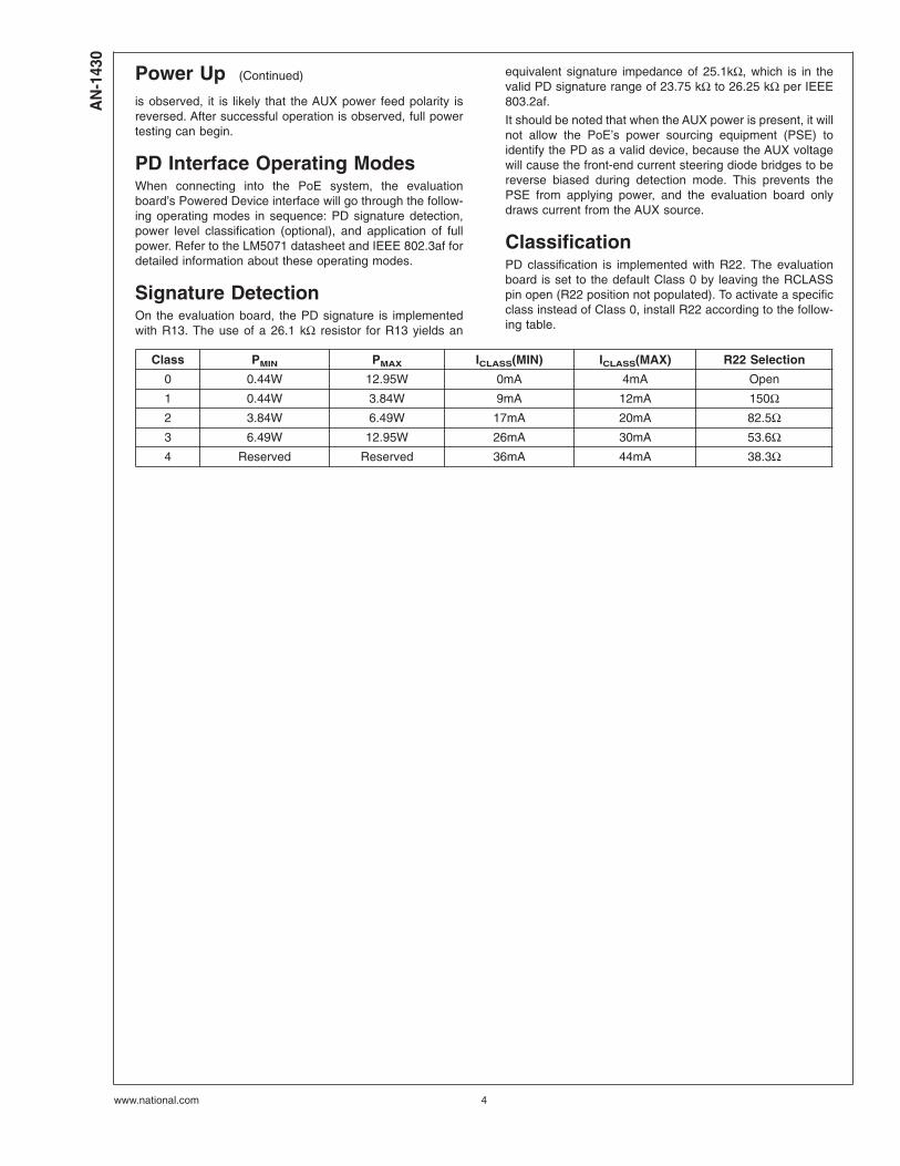
ClassificationPD classification is implemented with R22. The evaluationboard is set to the default Class 0 by leaving the RCLASSpin open (R22 position not populated). To activate a specificclass instead of Class 0, install R22 according to the follow-ing table.
Class PMIN PMAX ICLASS(MIN) ICLASS(MAX) R22 Selection
Input UVLO and UVLO HysteresisThe input UVLO threshold and UVLO hysteresis can beindependently programmed by selecting R5 and R37. TheUVLO release threshold level is mainly determined by theratio of R37 and R5, as governed by the following equation,
where VF stands for the forward voltage drop of a singlediode of the input current steering bridge. The UVLO hyster-esis is determined by the following equation:
UVLO_hysteresis = 10µA x R5
The evaluation board uses 33.2 kΩ for R37 and 590 kΩ forR5, setting the UVLO release threshold at about 39V and aUVLO hysteresis of 5.9V. The use of C1 helps filter out inputvoltage transients, thus preventing faulty activation or re-lease of the input UVLO.
AUX Power OptionFor AUX power option, the circuitry tied to the AUX pin forcesthe UVLO to release in order to allow operation at an AUXvoltage as low as 10.5V (9.5V seen by the VIN pin of theLM5071 IC). Note that the AUX pin references VEE while theauxiliary supply references RTN, which will be different byone diode drop until the internal hot swap MOSFET is en-gaged.
It is required that D2 be installed when the AUX input is lowerthan 14V. This will bypass the internal startup regulator anddirectly supply the bias voltage to the LM5071 IC for startup.Use CMHD4448 or equivalent for D2. When the switchingcircuit establishes stable operation, Vcc will be provided by atransformer winding with a level up to 16V. This voltage maydamage the internal startup regulator by back feeding to thelower potential VIN line. To solve this problem, D3 is intro-duced to protect the IC by bypassing the back feed path andclamping the VCC pin. On the evaluation board, D3 hasalready been installed. However, for applications where theinput voltage is always higher than 18V, D3 can be removedto save the BOM cost.
Small value resistors in series with the auxiliary input limitthe inrush current from the auxiliary supply. They should bemade as large as is practical given the design constraints.
Special attention should be paid to the selection of D1, D2,D3, D4 and Q3. They all should be low leakage currentdevices. Otherwise the leakage current during PoE opera-tion will create a false signal at the AUX pin of the IC as if thecircuit is powered from the AUX source. Most diode andtransistor datasheets provide information on the maximumleakage current at both 25˚C and 125˚C, although the datafor the intermediate temperatures are not often given. It canbe approximated that the leakage current doubles for every10˚C temperature rise.
The junction temperature of these devices should not reach125˚C because the only dissipation inside these devices isdue to the leakage current. Therefore it is not necessary toselect the devices based on the maximum leakage currentspecified at 125˚C. The evaluation board design considered
55˚C as the maximum junction temperature of these de-vices, which is true for most PoE applications. At 55˚C, theselection of S3BB-13 for D1, CRH01 for D3, CMHD4448 forD4 and CMPT5401 for Q3, will not cause a false signal atAUX pin.
When designing a PD for the higher temperature require-ment of some particular application, the values of R19, R23,R29 and R30 should be chosen such that the voltage cre-ated across R19 does not exceed 0.5V during PoE opera-tion.
The AUX pin is not reverse protected, and an additionalreverse blocking diode will be required for complete auxiliaryinput reverse protection.
Flyback Converter TopologyThe dc-dc converter stage of the LM5071 evaluation boardfeatures the flyback topology, which employs the minimumnumber of power components to implement an isolatedpower supply at the lowest possible cost.
A unique characteristic of the flyback topology is its powertransformer. Unlike an ordinary power transformer that si-multaneously transfers the power from the primary to thesecondary, the flyback transformer first stores the energy inthe transformer core every switching cycle when the mainswitch is turned on; and then releases the stored energy tothe load during the rest of the cycle. When the stored energyis not completely released before the main switch is turnedon again, it is said that the flyback converter operates incontinuous conduction mode (CCM). Otherwise, it is in dis-continuous conduction mode (DCM).
Major advantages of CCM over DCM include (i) lower ripplecurrent and ripple voltage, requiring smaller input and outputfilter capacitors; and (ii) lower rms current, thus reducing theconduction losses. To keep the flyback converter in CCM atlight load, the transformer’s primary inductance should bedesigned as large as is practical.
Major drawbacks of CCM, as compared to DCM, are (i) thepresence of the Right-Half-Plane Zero which may limit theachievable bandwidth of the feedback loop; and (ii) the needfor slope compensation to stabilize the feedback loop at dutycycles greater than 50%. The flyback topology can havemultiple secondary windings for multi output channels. Oneor more of these secondary channels are normally utilizedinternally by the converter itself to provide necessary biasvoltages for the controller and other devices.
The evaluation board uses a small power transformer havinga primary inductance of 32 µH. This is a compromise madeto allow the small transformer to operate over a wide inputvoltage range from 14V to 60V. However, with this trans-former, the flyback converter runs in CCM at full load forinput voltages lower than 42V, and in DCM for higher inputvoltages or light loads. The LM5071’s built-in slope compen-sation helps stabilize the feedback loop when the duty cycleexceeds 50% in the low input voltage range.
A transformer winding is used to provide the bias voltage(VCC) to the LM5071 IC. Although the LM5071 controllerincludes an internal startup regulator which can support thebias requirement indefinitely, the transformer winding pro-duces a VCC about 2V higher than the startup regulatoroutput, thus shutting off the startup regulator and reducingthe power dissipation inside the IC.
AN
-1430
www.national.com5
The Factors Limiting the MinimumOperating Input VoltageThe LM5071 is capable of operating with an AUX powersource of as low as 10.5V (after the AUX input OR-ing-diodedrop, the VIN pin sees 9.5V). However, the minimum oper-ating AUX input voltage of the evaluation board at full load ismainly determined by two factors; the flyback power trans-former design and the values of the current sense resistorsR14 and R15.
The installed EP13 type power transformer (DA2257-AL orDCT13EP-U12S005) is a low cost solution to operate with awide AUX input voltage range. However, the small cross-sectional area of the EP13 magnetic core limits the maxi-mum flux it can handle. To use such a small transformer from14V to 60V under the full load condition, a compromisebetween the minimum operating input voltage and maximuminductance of the transformer must be made such that thepeak current at 14V input will not cause the peak flux densityto exceed 3000 Gauss. A drawback of this low cost solutionis that the rms currents flowing through the dc-dc converterstage are increased and the efficiency of the dc-dc converteris reduced by about 3%.
Replacing the originally installed transformer with the op-tional power transformer DA2383-AL from Coilcraft improvesthe efficiency, but the minimum operating input voltage willbe limited to 24V. To use this optional transformer for lowerinput voltage, the load level should be scaled down accord-ingly, as shown in Figure 3.
To optimize efficiency over the maximum input voltage rangeof 9.5V to 60V, a larger magnetic core like the EFD20 shouldbe used. The EFD20 core has adequate cross-sectionalarea to handle the peak currents at 9.5V input.
The effects of the current sense resistors R14 and R15 alsolimit the minimum AUX input operating voltage. TheLM5071’s internal slope compensation stabilizes the feed-back loop of the dc-dc converter when the duty cycle ex-ceeds 50% for input voltages lower than 22V. However, therelative magnitude of the slope compensation is inverselyproportional to the values of R14 and R15. The maximumvalues of R14 and R15 are governed by the following rela-tion:
where
Dmax is the duty cycle at the minimum AUX input voltage
fsw the switching frequency, in kHz
Lm the flyback transformer primary inductance, in µH
kt the transformer’s primary to secondary turns ratio
Vo the output voltage, in volts
VF the forward drop of the output diode D5, in volts
Selecting 0.30Ω for both R14 and R15 will allow a minimumoperating voltage of 14V. For lower AUX input voltage, Dmaxis greater and hence R14 and R15 must be reduced accord-ingly. However, the smaller resistors increase the slope com-pensation. Increasing the slope compensating makes thefeedback loop appear more like voltage mode than currentmode which requires the use of a low ESR capacitor for C16rather than the low cost capacitor initially installed on theevaluation board.
In summary, the 14V minimum operating AUX input voltageof the evaluation board is limited by the low cost solution. Inorder to use the evaluation board with a lower AUX source,the power transformer T1, the output capacitor C16, R14and R15 should be all modified in addition to the installationof D2.
Performance Characteristics
POWER UP SEQUENCE
The high level of integration designed into the LM5071 al-lows all power sequencing communications to occur withinthe IC. Very little system management design is required bythe user. The power up sequence is as follows. Note that theRTN pin (IC pin 8) is isolated from the +3.3V RTN output pinof the board:
1. Before power up, all nodes in the non-isolated section ofthe power supply remain at high potential until UVLO isreleased and the drain of the internal hot swap MOSFETis pulled down to VEE (IC pin 7).
2. Once the RTN pin of the IC drops below 1.5V (refer-enced to VEE), the VCC regulator is released and al-lowed to start. This signals the assertion of the internal“Power Good” signal. The VCC regulator ramps at a rateequal to its current limit, typically 20 mA, divided by theVCC load capacitance, C19.
3. Once the VCC regulator is within minimum regulation,about 7.6V referenced to RTN, the soft-start pin is re-leased. The soft-start pin will rise at a rate equal to thesoft-start current source, typically 10µA, divided by thesoft-start pin capacitance, C26.
4. As the switching regulator achieves regulation, the aux-iliary winding will raise the VCC voltage to about 10V,thus shutting down the internal regulator and increasingefficiency.
Figure 4 shows the voltages at RTN, VCC, and SS (Soft-start) IC pins, all referenced to the VEE pin, during a normalstartup sequence. A more detailed scope plot of the VCC
regulator starting up is given in Figure 5. The auxiliary wind-ing starts to supply a higher voltage as the switching regu-lator output voltage rises.
20175804
FIGURE 3. Maximum Load Current vs. Minimum InputVoltage as Limited by Different EP13 Type Power
Transformers
AN
-143
0
www.national.com 6
Performance Characteristics(Continued)
Figure 6 shows a normal 3.3V line startup, along with thesoftstart pin for reference.
OUTPUT DEAD SHORT FAULT RESPONSE
The evaluation board survives the output dead short condi-tion by running into a re-try mode (hiccups). Applying a deadshort to the +3.3V line causes a number of protectionmechanisms to occur sequentially. They are:
1. Feedback raises duty cycle in an attempt to maintain theoutput voltage. This initiates cycle-by-cycle over-currentlimiting which turns off the main switch when the currentsense (CS) pin exceeds the current limit threshold.
2. The average current in the internal PD interface MOS-FET rises until it is current limited around 390 mA. Someovershoot in the current will be observed, as it takes timefor the current limit amplifier to react and change theoperating mode of the MOSFET.
3. Because linear current limit is accomplished by drivingthe MOSFET into the saturation region, the drain voltage(RTN pin) rises. When it reaches 2.5V with respect toVEE, the internal power good signal is de-asserted.
4. The de-assertion of power good causes the discharge ofthe soft-start capacitor, which disables all switching ac-tion in the dc-dc converter.
5. Once the switching stops, the current in the internalMOSFET will decrease and the drain voltage will fallback below 1.5V with respect to VEE. When power goodis re-asserted, the dc-dc converter will automaticallyrestart with a new soft-start sequence.
The re-try mode due to a shorted output condition can beobserved in Figure 7. The soft-start pin is observed to risequickly as the LM5071 reacts to the fault. This is because itreferences RTN, while all scope measurements referenceVEE.
20175806
Horizontal Resolution: 5 ms/Div.
Trace 1: RTN pin, elevated until UVLO release. 5V/Div.
Trace 2: SS pin, starts when VCC achieves minimum regu-lation. 5V/Div.
Trace 3: VCC, starts when RTN<1.5V, elevated by auxiliarywinding. 5V/Div.
FIGURE 4. Normal Startup Sequence
20175807
Horizontal Resolution: 2 ms/Div.
Trace 1: RTN pin, elevated until UVLO release. 5V/Div.
Trace 2: Vout, cross-regulate VCC after output regulation isestablished. 1V/Div.
Trace 3: VCC, starts when RTN<1.5V, elevated by auxiliarywinding. 2V/Div.
FIGURE 5. VCC Startup Detail
20175808
Horizontal Resolution: 1 ms/Div.
Trace 1: +3.3V output voltage, 1V/Div.
Trace 2: Softstart pin, 1V/Div.
Trace 3: Input current (AC coupled), 200 mA/Div.
FIGURE 6. Regulator Output (+3.3V) Startup Detail
AN
-1430
www.national.com7
Performance Characteristics(Continued)
STEP RESPONSE
Figure 8 shows the step load response at VIN = 48V.
RIPPLE VOLTAGE/CURRENT
Figure 9 shows the output ripple voltage and input ripplecurrent for 48V input voltage and 3.3A output.
FLYBACK TRANSFORMER WAVEFORMS
Figure 10 and Figure 11 show the typical drain to sourcevoltage of the main switch Q1 and the reverse voltage ofrectifier diode D5, respectively, at 48V input voltage and3.3A output.
Trace 1: Drain to source voltge of main switch Q1, 50V/Div.
FIGURE 10. Flyback Main Switch Drain VoltageWaveform
AN
-143
0
www.national.com 8
Performance Characteristics(Continued)
Reconfiguration Of The EvaluationBoard For 3.3V And 5V DualOutputsThe standard evaluation circuit can be easily reconfiguredinto a 2A 3.3V and 0.6A 5.5V, dual output power supply. Thereconfiguration needs to populate the components for the5.5V output rail, as shown in Figure 12. These componentsare listed in the additional BOM list in the Appendix.
Reconfiguration Of The EvaluationBoard for Non-Isolated OutputApplicationsFor applications where output isolation is not required, thenon-isolated version of the evaluation board can be used to
reduce the BOM cost. Reconfiguration of the circuit board tothe non-isolated version can be accomplished in the follow-ing four steps (refer to Figure 1 if not indicated otherwise):
1. Delete the unused parts from the circuit board as well asthe BOM: C20, C22, C25, C28, R7, R11, R16, R17, R24,U2 and U3.
2. Connect test points P5 and P6 with a bus wire of AWG26 (refer to Figure 13).
3. Short C28 pads by installing a 0Ω resistor of R2010 size,or by soldering a piece of AWG 26 bus wire.
4. Change C30 to 3.3 nF, C31 to 1.0 nF and R20 to 10 kΩ.
Figure 13 shows the schematic of non-isolated circuit for asingle 3.3V output. Similar changes also apply to the dualoutput version.
Enhancing Input FilterPerformanceThe evaluation board employs two 4.7 µF ceramic capaci-tors (C4 and C5) as the input filter of the DC-DC converterstage. The configuration is adequate to meet the IEEE802.3af specifications, though it may be required to furtherenhance the input filter performance for EMI / EMC consid-erations. To do so, an inductor of 10 µH such as the CoilcraftDO3308P-103MLD can be added. The inductor should beinstalled in the L1 location on the top side of the PC Board,a location originally shorted with a bus wire. Also, install a 22µF aluminum electrolytic capacitor such as the PanasonicEEV-HA2A220P in the C6 location right beside L1 on the topside of the PC Board in order to protect the LM5072 IC byabsorbing the inductor energy during shutdown. A jumperwire of AWG #28 or thicker with insulation sleeve should besoldered to connect the junction of L1 / BR1 with the junctionof C6 / R27. By doing so, the 22 µF capacitor is placed infront of L1 and directly across the VIN and RTN pins of theLM5072. As a cost consideration, ceramic capacitor C5 (4.7µF) can be deleted from the PCB, and L1 and C4 will beadequate to attenuate the input ripple current below 2 mApeak to peak .
20175813
Horizontal Resolution: 1 µs/Div.
Trace 1: Reverse voltage across output rectifier diode D5,5V/Div.
A Note For Using The EfficiencyOptimized EP13 PowerTransformer DA2383Please note that the DA2383 is a single output transformer.When using a DA2383 to obtain better efficiency (See Figure3 for the applicable load and AUX input voltage levels), D5should be removed and installed onto the Q2 pads on the topside of the evaluation board. This is because the secondarywinding of DA2382 uses Pins 6 through 9 of the transformerbobbin, unlike DA2257 that only uses of Pins 7 and 8 for thesecondary winding. The maximum converter stage efficiencyat 3.3A will be expected to be greater than 84%.
A Few More Hints On ImprovingThe EfficiencySince the evaluation board is designed as a low cost solu-tion, upgrading the following components with slightly moreexpensive devices will increase the efficiency.
(i) Use SUD15N15-95 for Q1; a faster device than theinstalled SUD25N15-52, to improve the dc-dc converter ef-ficiency by 1%
(ii) Use DFLS1100 for D1; a 100V 1A high voltageSchottky barrier rectifier with low leakage current, to in-crease the AUX operation’s end-to-end efficiency by at least1%. This is suitable for an AUX input voltage greater than15V.
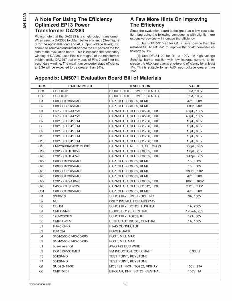
Appendix: LM5071 Evaluation Board Bill of Materials
ITEM PART NUMBER DESCRIPTION VALUE
BR1 CBRHD-01 DIODE BRIDGE, SMDIP, CENTRAL 0.5A, 100V
BR2 CBRHD-01 DIODE BRIDGE, SMDIP, CENTRAL 0.5A, 100V
C17 EMVY100ADA101MF55G CAPACITOR, AL ELEC, CHEMI-ON 100µF, 10V
D8 CMSH2-60 DIODE, SMA, CENTRAL 2A, 60V
J6 3104-2-00-01-00-00-080 POST, MILL MAX
J7 3104-2-00-01-00-00-080 POST, MILL MAX
L2 DO1813P-181MLD SM INDUCTOR, COILCRAFT 0.18µH
Z4 CMZ5920B ZENER, SMA, CENTRAL 6.2V
Note: The total load of the dual outputs should be limited below 10W maximum.
National does not assume any responsibility for use of any circuitry described, no circuit patent licenses are implied and National reservesthe right at any time without notice to change said circuitry and specifications.
For the most current product information visit us at www.national.com.
LIFE SUPPORT POLICY
NATIONAL’S PRODUCTS ARE NOT AUTHORIZED FOR USE AS CRITICAL COMPONENTS IN LIFE SUPPORT DEVICES OR SYSTEMSWITHOUT THE EXPRESS WRITTEN APPROVAL OF THE PRESIDENT AND GENERAL COUNSEL OF NATIONAL SEMICONDUCTORCORPORATION. As used herein:
1. Life support devices or systems are devices or systemswhich, (a) are intended for surgical implant into the body, or(b) support or sustain life, and whose failure to perform whenproperly used in accordance with instructions for useprovided in the labeling, can be reasonably expected to resultin a significant injury to the user.
2. A critical component is any component of a life support deviceor system whose failure to perform can be reasonablyexpected to cause the failure of the life support device orsystem, or to affect its safety or effectiveness.
BANNED SUBSTANCE COMPLIANCE
National Semiconductor manufactures products and uses packing materials that meet the provisions of the Customer ProductsStewardship Specification (CSP-9-111C2) and the Banned Substances and Materials of Interest Specification (CSP-9-111S2) and containno ‘‘Banned Substances’’ as defined in CSP-9-111S2.
Leadfree products are RoHS compliant.
National SemiconductorAmericas CustomerSupport CenterEmail: [email protected]: 1-800-272-9959
National SemiconductorEurope Customer Support Center