12
LM3407 Application Note 1763 LM3407 Evaluation Board Reference Design Literature Number: SNVA308A
LM3407
Application Note 1763 LM3407 Evaluation Board Reference Design
Literature Number: SNVA308A
LM3407 Evaluation BoardReference Design
National SemiconductorApplication Note 1763SH WongJanuary 21, 2009
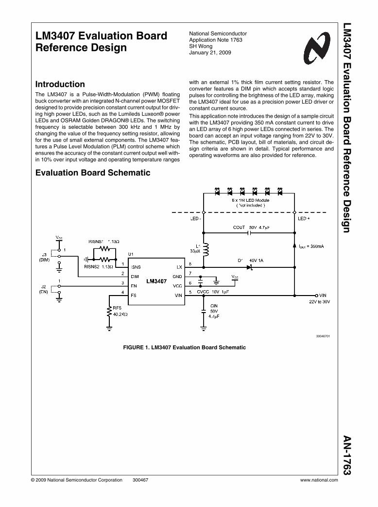
IntroductionThe LM3407 is a Pulse-Width-Modulation (PWM) floatingbuck converter with an integrated N-channel power MOSFETdesigned to provide precision constant current output for driv-ing high power LEDs, such as the Lumileds Luxeon® powerLEDs and OSRAM Golden DRAGON® LEDs. The switchingfrequency is selectable between 300 kHz and 1 MHz bychanging the value of the frequency setting resistor, allowingfor the use of small external components. The LM3407 fea-tures a Pulse Level Modulation (PLM) control scheme whichensures the accuracy of the constant current output well with-in 10% over input voltage and operating temperature ranges
with an external 1% thick film current setting resistor. Theconverter features a DIM pin which accepts standard logicpulses for controlling the brightness of the LED array, makingthe LM3407 ideal for use as a precision power LED driver orconstant current source.
This application note introduces the design of a sample circuitwith the LM3407 providing 350 mA constant current to drivean LED array of 6 high power LEDs connected in series. Theboard can accept an input voltage ranging from 22V to 30V.The schematic, PCB layout, bill of materials, and circuit de-sign criteria are shown in detail. Typical performance andoperating waveforms are also provided for reference.
Evaluation Board Schematic
30046701
FIGURE 1. LM3407 Evaluation Board Schematic
© 2009 National Semiconductor Corporation 300467 www.national.com
LM
3407 E
valu
atio
n B
oard
Refe
ren
ce D
esig
nA
N-1
763
30046702
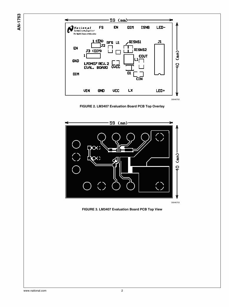
FIGURE 2. LM3407 Evaluation Board PCB Top Overlay
30046703
FIGURE 3. LM3407 Evaluation Board PCB Top View
www.national.com 2
AN
-1763
30046704
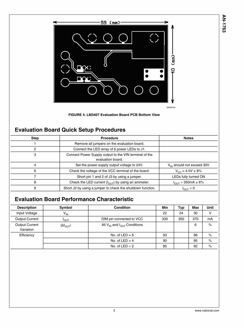
FIGURE 4. LM3407 Evaluation Board PCB Bottom View
Evaluation Board Quick Setup Procedures
Step Procedure Notes
1 Remove all jumpers on the evaluation board.
2 Connect the LED array of 6 power LEDs to J1.
3 Connect Power Supply output to the VIN terminal of the
evaluation board.
4 Set the power supply output voltage to 24V. VIN should not exceed 30V
6 Check the voltage of the VCC terminal of the board. VCC = 4.5V ± 8%
7 Short pin 1 and 2 of J3 by using a jumper. LEDs fully turned ON
8 Check the LED current (IOUT) by using an ammeter. IOUT = 350mA ± 6%
9 Short J2 by using a jumper to check the shutdown function. IOUT = 0
Evaluation Board Performance Characteristic
Description Symbol Condition Min Typ Max Unit
Input Voltage VIN 22 24 30 V
Output Current IOUT DIM pin connected to VCC 330 350 370 mA
Output Current
Variation|ΔIOUT| All VIN and IOUT Conditions 6 %
Efficiency No. of LED = 6 93 96 %
No. of LED = 4 90 95 %
No. of LED = 2 85 92 %
3 www.national.com
AN
-1763
Design Procedure
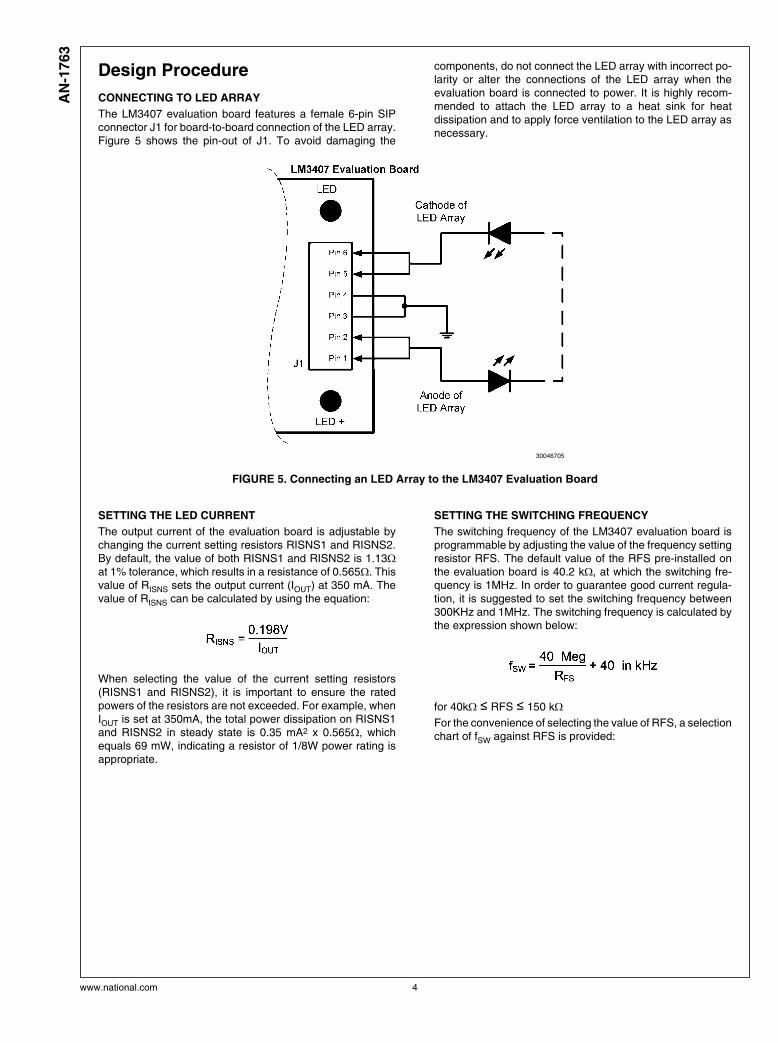
CONNECTING TO LED ARRAY
The LM3407 evaluation board features a female 6-pin SIPconnector J1 for board-to-board connection of the LED array.Figure 5 shows the pin-out of J1. To avoid damaging the
components, do not connect the LED array with incorrect po-larity or alter the connections of the LED array when theevaluation board is connected to power. It is highly recom-mended to attach the LED array to a heat sink for heatdissipation and to apply force ventilation to the LED array asnecessary.
30046705
FIGURE 5. Connecting an LED Array to the LM3407 Evaluation Board
SETTING THE LED CURRENT
The output current of the evaluation board is adjustable bychanging the current setting resistors RISNS1 and RISNS2.By default, the value of both RISNS1 and RISNS2 is 1.13Ωat 1% tolerance, which results in a resistance of 0.565Ω. Thisvalue of RISNS sets the output current (IOUT) at 350 mA. Thevalue of RISNS can be calculated by using the equation:
When selecting the value of the current setting resistors(RISNS1 and RISNS2), it is important to ensure the ratedpowers of the resistors are not exceeded. For example, whenIOUT is set at 350mA, the total power dissipation on RISNS1and RISNS2 in steady state is 0.35 mA2 x 0.565Ω, whichequals 69 mW, indicating a resistor of 1/8W power rating isappropriate.
SETTING THE SWITCHING FREQUENCY
The switching frequency of the LM3407 evaluation board isprogrammable by adjusting the value of the frequency settingresistor RFS. The default value of the RFS pre-installed onthe evaluation board is 40.2 kΩ, at which the switching fre-quency is 1MHz. In order to guarantee good current regula-tion, it is suggested to set the switching frequency between300KHz and 1MHz. The switching frequency is calculated bythe expression shown below:
for 40kΩ ≤ RFS ≤ 150 kΩFor the convenience of selecting the value of RFS, a selectionchart of fSW against RFS is provided:
www.national.com 4
AN
-1763
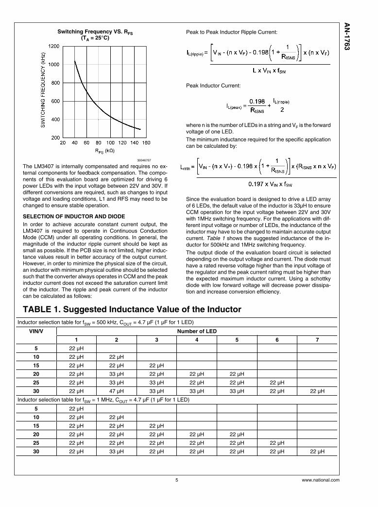
Switching Frequency VS. RFS(TA = 25°C)
30046707
The LM3407 is internally compensated and requires no ex-ternal components for feedback compensation. The compo-nents of this evaluation board are optimized for driving 6power LEDs with the input voltage between 22V and 30V. Ifdifferent conversions are required, such as changes to inputvoltage and loading conditions, L1 and RFS may need to bechanged to ensure stable operation.
SELECTION OF INDUCTOR AND DIODE
In order to achieve accurate constant current output, theLM3407 is required to operate in Continuous ConductionMode (CCM) under all operating conditions. In general, themagnitude of the inductor ripple current should be kept assmall as possible. If the PCB size is not limited, higher induc-tance values result in better accuracy of the output current.However, in order to minimize the physical size of the circuit,an inductor with minimum physical outline should be selectedsuch that the converter always operates in CCM and the peakinductor current does not exceed the saturation current limitof the inductor. The ripple and peak current of the inductorcan be calculated as follows:
Peak to Peak Inductor Ripple Current:
Peak Inductor Current:
where n is the number of LEDs in a string and VF is the forwardvoltage of one LED.
The minimum inductance required for the specific applicationcan be calculated by:
Since the evaluation board is designed to drive a LED arrayof 6 LEDs, the default value of the inductor is 33µH to ensureCCM operation for the input voltage between 22V and 30Vwith 1MHz switching frequency. For the applications with dif-ferent input voltage or number of LEDs, the inductance of theinductor may have to be changed to maintain accurate outputcurrent. Table 1 shows the suggested inductance of the in-ductor for 500kHz and 1MHz switching frequency.
The output diode of the evaluation board circuit is selecteddepending on the output voltage and current. The diode musthave a rated reverse voltage higher than the input voltage ofthe regulator and the peak current rating must be higher thanthe expected maximum inductor current. Using a schottkydiode with low forward voltage will decrease power dissipa-tion and increase conversion efficiency.
TABLE 1. Suggested Inductance Value of the Inductor
Inductor selection table for fSW = 500 kHz, COUT = 4.7 µF (1 µF for 1 LED)
VIN/V Number of LED
1 2 3 4 5 6 7
5 22 µH
10 22 µH 22 µH
15 22 µH 22 µH 22 µH
20 22 µH 33 µH 22 µH 22 µH 22 µH
25 22 µH 33 µH 33 µH 22 µH 22 µH 22 µH
30 22 µH 47 µH 33 µH 33 µH 33 µH 22 µH 22 µH
Inductor selection table for fSW = 1 MHz, COUT = 4.7 µF (1 µF for 1 LED)
5 22 µH
10 22 µH 22 µH
15 22 µH 22 µH 22 µH
20 22 µH 22 µH 22 µH 22 µH 22 µH
25 22 µH 22 µH 22 µH 22 µH 22 µH 22 µH
30 22 µH 33 µH 22 µH 22 µH 22 µH 22 µH 22 µH
5 www.national.com
AN
-1763
LED DIMMING
There are two ways to disable the current output (IOUT) of theevaluation board circuit. The current output of the LM3407evaluation board can be disabled by connecting either theDIM or EN pin to ground. Connecting the EN pin to groundwill shutdown the internal linear regulator and maintain mini-mal power consumption. Connecting the DIM pin to groundwill only disable the current output of the LM3407, while theinternal oscillator and control circuits remain active to facilitatefast wake up.
In general, dimming of the LED array can be achieved by ap-plying a logic pulse chain to the DIM terminal of the evaluationboard to periodically enable and disable the LM3407 andcontrol the average IOUT of the LED array. Since the colorcharacteristics of a LED are closely related to the driving cur-rent, dimming by adjusting the current setting resistor causesthe color temperature to drift. To control the brightness of theLED array effectively, PWM dimming should be used. PWMdimming is a dimming method which controls the ON/OFFtime ratio of the LED(s) at fixed frequency.
The DIM terminal on the evaluation board is directly connect-ed to the DIM pin of the LM3407, which provides a PWMsignal input for dimming of the LED array. In order to properlyenable and disable the LM3407, the PWM dimming signal
should have a logic low of 1V maximum and logic high of 2Vminimum. The DIM terminal is internally pulled down toground by a 400 kΩ resistor, which should be connected toeither logic high or low and should not be left open. In steadystate, the expression of the average LED driving current is:
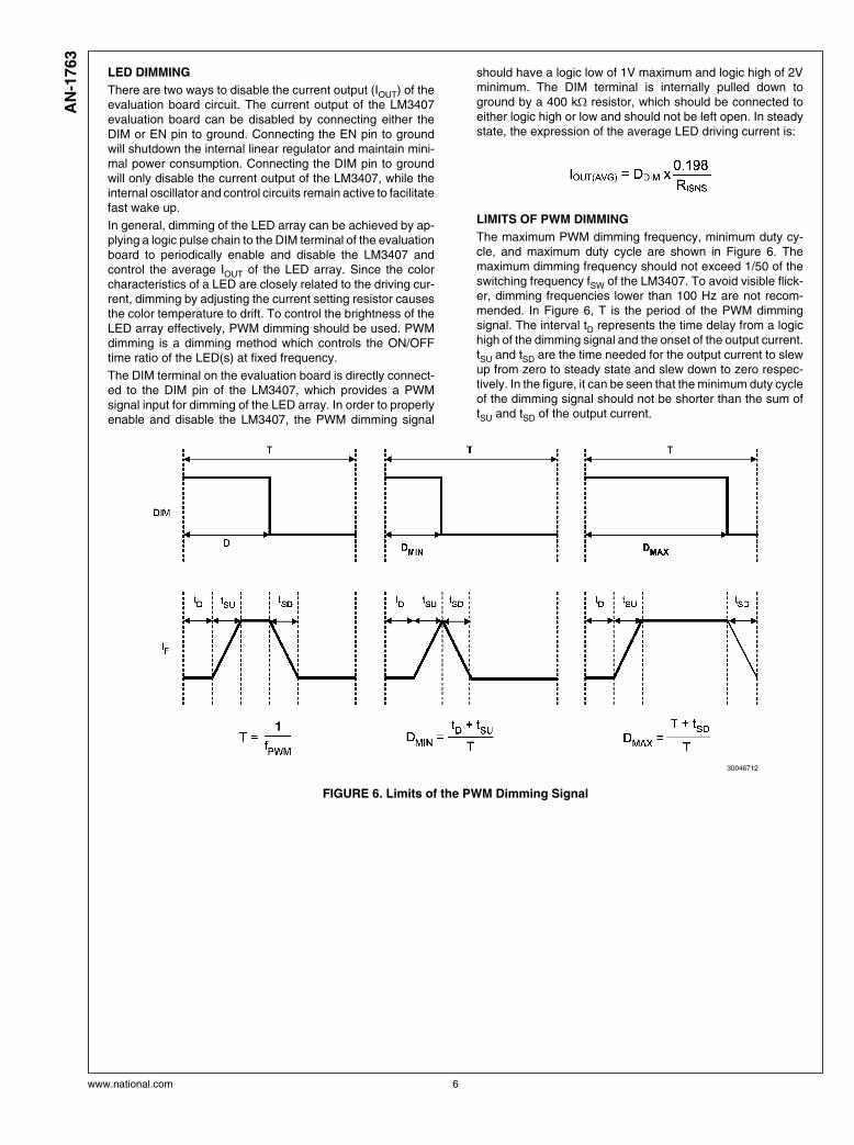
LIMITS OF PWM DIMMING
The maximum PWM dimming frequency, minimum duty cy-cle, and maximum duty cycle are shown in Figure 6. Themaximum dimming frequency should not exceed 1/50 of theswitching frequency fSW of the LM3407. To avoid visible flick-er, dimming frequencies lower than 100 Hz are not recom-mended. In Figure 6, T is the period of the PWM dimmingsignal. The interval tD represents the time delay from a logichigh of the dimming signal and the onset of the output current.tSU and tSD are the time needed for the output current to slewup from zero to steady state and slew down to zero respec-tively. In the figure, it can be seen that the minimum duty cycleof the dimming signal should not be shorter than the sum oftSU and tSD of the output current.
30046712
FIGURE 6. Limits of the PWM Dimming Signal
www.national.com 6
AN
-1763
PCB LAYOUT GUIDE
Since copper traces of PCBs carry resistance and parasiticinductance, the longer the copper trace, the higher the resis-tance and inductance. These factors introduce voltage andcurrent spikes to the switching nodes and impair the perfor-mance of the whole circuit. To optimize the performance ofthe LM3407, the rule of thumb is to keep the connections be-tween components as short and direct as possible. Since trueaverage current regulation is achieved by detecting the aver-age switch current, the current setting resistors RISNS1 andRISNS2 must be located as close to the LM3407 as possibleto reduce the parasitic inductance of the copper trace andavoid noise pick-up. The connections between LX pin, recti-
fier D1, inductor L1 and output capacitor COUT should bekept as short as possible to reduce the voltage spikes at theLX pin. CVCC is the output filter capacitor for the internal lin-ear regulator of the LM3407, it is recommended to be placedclose to the pin VCC. The input filter capacitor CIN should belocated close to L1 and the cathode of D1. If CIN is connectedto the VIN pin by a long trace, a 0.1µF capacitor should beadded close to pin VIN for noise filtering. In normal operation,heat will be generated inside the LM3407 and may damagethe device if no thermal management is applied. For moredetail on switching power supply layout considerations seeApplication Note AN-1149: Layout Guidelines for SwitchingPower Supplies.
Bill of Materials
Designation Description Package Manufacture Part # Vendor
U1 LED Driver IC, LM3407 eMSOP-8 LM3407 NSC
L1 Inductor 33µH 0.58A 4.0 x 4.0 x 1.8 (mm) LPS4018-333ML Coilcraft
* Inductor 33µH 0.56A 4.8 x 4.3 x 3.5 (mm) CR43NP-330K Sumida
D1 Schottky Diode 40V 1.0A DO-214AC (SMA) SS14 Vishay
CIN, COUT Cap MLCC 50V 4.7µF X7R 1210 GRM32ER71H475K88L Murata
CVCC Cap MLCC 10V 1.0µF X5R 0805 GRM188R61A105KA61D Murata
RISNS1, RISNS2 Chip Resistor 1.13Ω 1% 0805 CRCW08051R13F Vishay
RFS Chip Resistor 40.2kΩ 1% 0805 CRCW08054022F Vishay
J1 6-pin Connector DIP-12 535676-5 Tyco Electronics
J2 2-way Jumper System 2.54 (mm) Pitch
J3 3-way Jumper System 2.54 (mm) Pitch
VCC, GND, EN, DIM,
ISNS, LX
Terminal pin 2.29 (mm) Dia. 160-1026 Cambion
VIN, GND Terminal pin 1.57 (mm) Dia. 160-1512 Cambion
PCB LM3407 Evaluation Board 59 x 40 (mm) NSC
J3 2-pin Jumper
*Alternative Supplier
7 www.national.com
AN
-1763
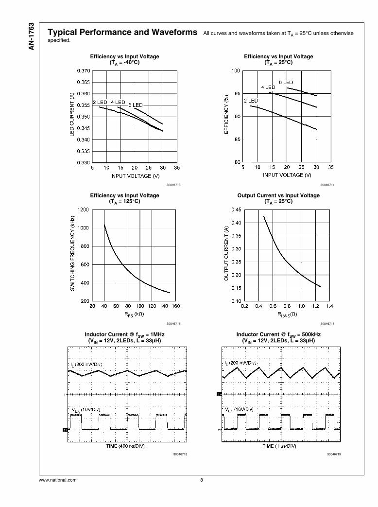
Typical Performance and Waveforms All curves and waveforms taken at TA = 25°C unless otherwise
specified.
Efficiency vs Input Voltage(TA = -40°C)
30046713
Efficiency vs Input Voltage(TA = 25°C)
30046714
Efficiency vs Input Voltage(TA = 125°C)
30046715
Output Current vs Input Voltage(TA = 25°C)
30046716
Inductor Current @ fSW = 1MHz(VIN = 12V, 2LEDs, L = 33µH)
30046718
Inductor Current @ fSW = 500kHz(VIN = 12V, 2LEDs, L = 33µH)
30046719
www.national.com 8
AN
-1763
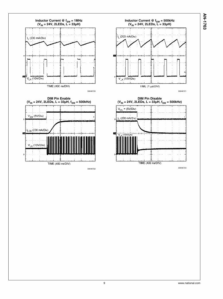
Inductor Current @ fSW = 1MHz(VIN = 24V, 2LEDs, L = 33µH)
30046720
Inductor Current @ fSW = 500kHz(VIN = 24V, 2LEDs, L = 33µH)
30046721
DIM Pin Enable(VIN = 24V, 2LEDs, L = 33µH, fSW = 500kHz)
30046722
DIM Pin Disable(VIN = 24V, 2LEDs, L = 33µH, fSW = 500kHz)
30046723
9 www.national.com
AN
-1763
NotesA
N-1
763
LM
3407 E
valu
ati
on
Bo
ard
Refe
ren
ce D
esig
n
For more National Semiconductor product information and proven design tools, visit the following Web sites at:
Products Design Support
Amplifiers www.national.com/amplifiers WEBENCH® Tools www.national.com/webench
Audio www.national.com/audio App Notes www.national.com/appnotes
Clock and Timing www.national.com/timing Reference Designs www.national.com/refdesigns
Data Converters www.national.com/adc Samples www.national.com/samples
Interface www.national.com/interface Eval Boards www.national.com/evalboards
LVDS www.national.com/lvds Packaging www.national.com/packaging
Power Management www.national.com/power Green Compliance www.national.com/quality/green
Switching Regulators www.national.com/switchers Distributors www.national.com/contacts
LDOs www.national.com/ldo Quality and Reliability www.national.com/quality
LED Lighting www.national.com/led Feedback/Support www.national.com/feedback
Voltage Reference www.national.com/vref Design Made Easy www.national.com/easy
PowerWise® Solutions www.national.com/powerwise Solutions www.national.com/solutions
Serial Digital Interface (SDI) www.national.com/sdi Mil/Aero www.national.com/milaero
Temperature Sensors www.national.com/tempsensors Solar Magic® www.national.com/solarmagic
Wireless (PLL/VCO) www.national.com/wireless Analog University® www.national.com/AU
THE CONTENTS OF THIS DOCUMENT ARE PROVIDED IN CONNECTION WITH NATIONAL SEMICONDUCTOR CORPORATION(“NATIONAL”) PRODUCTS. NATIONAL MAKES NO REPRESENTATIONS OR WARRANTIES WITH RESPECT TO THE ACCURACYOR COMPLETENESS OF THE CONTENTS OF THIS PUBLICATION AND RESERVES THE RIGHT TO MAKE CHANGES TOSPECIFICATIONS AND PRODUCT DESCRIPTIONS AT ANY TIME WITHOUT NOTICE. NO LICENSE, WHETHER EXPRESS,IMPLIED, ARISING BY ESTOPPEL OR OTHERWISE, TO ANY INTELLECTUAL PROPERTY RIGHTS IS GRANTED BY THISDOCUMENT.
TESTING AND OTHER QUALITY CONTROLS ARE USED TO THE EXTENT NATIONAL DEEMS NECESSARY TO SUPPORTNATIONAL’S PRODUCT WARRANTY. EXCEPT WHERE MANDATED BY GOVERNMENT REQUIREMENTS, TESTING OF ALLPARAMETERS OF EACH PRODUCT IS NOT NECESSARILY PERFORMED. NATIONAL ASSUMES NO LIABILITY FORAPPLICATIONS ASSISTANCE OR BUYER PRODUCT DESIGN. BUYERS ARE RESPONSIBLE FOR THEIR PRODUCTS ANDAPPLICATIONS USING NATIONAL COMPONENTS. PRIOR TO USING OR DISTRIBUTING ANY PRODUCTS THAT INCLUDENATIONAL COMPONENTS, BUYERS SHOULD PROVIDE ADEQUATE DESIGN, TESTING AND OPERATING SAFEGUARDS.
EXCEPT AS PROVIDED IN NATIONAL’S TERMS AND CONDITIONS OF SALE FOR SUCH PRODUCTS, NATIONAL ASSUMES NOLIABILITY WHATSOEVER, AND NATIONAL DISCLAIMS ANY EXPRESS OR IMPLIED WARRANTY RELATING TO THE SALEAND/OR USE OF NATIONAL PRODUCTS INCLUDING LIABILITY OR WARRANTIES RELATING TO FITNESS FOR A PARTICULARPURPOSE, MERCHANTABILITY, OR INFRINGEMENT OF ANY PATENT, COPYRIGHT OR OTHER INTELLECTUAL PROPERTYRIGHT.
LIFE SUPPORT POLICY
NATIONAL’S PRODUCTS ARE NOT AUTHORIZED FOR USE AS CRITICAL COMPONENTS IN LIFE SUPPORT DEVICES ORSYSTEMS WITHOUT THE EXPRESS PRIOR WRITTEN APPROVAL OF THE CHIEF EXECUTIVE OFFICER AND GENERALCOUNSEL OF NATIONAL SEMICONDUCTOR CORPORATION. As used herein:
Life support devices or systems are devices which (a) are intended for surgical implant into the body, or (b) support or sustain life andwhose failure to perform when properly used in accordance with instructions for use provided in the labeling can be reasonably expectedto result in a significant injury to the user. A critical component is any component in a life support device or system whose failure to performcan be reasonably expected to cause the failure of the life support device or system or to affect its safety or effectiveness.
National Semiconductor and the National Semiconductor logo are registered trademarks of National Semiconductor Corporation. All otherbrand or product names may be trademarks or registered trademarks of their respective holders.
Copyright© 2009 National Semiconductor Corporation
For the most current product information visit us at www.national.com
National SemiconductorAmericas TechnicalSupport CenterEmail: [email protected]: 1-800-272-9959
National Semiconductor EuropeTechnical Support CenterEmail: [email protected] Tel: +49 (0) 180 5010 771English Tel: +44 (0) 870 850 4288
National Semiconductor AsiaPacific Technical Support CenterEmail: [email protected]
National Semiconductor JapanTechnical Support CenterEmail: [email protected]
www.national.com

IMPORTANT NOTICE
Texas Instruments Incorporated and its subsidiaries (TI) reserve the right to make corrections, modifications, enhancements, improvements,and other changes to its products and services at any time and to discontinue any product or service without notice. Customers shouldobtain the latest relevant information before placing orders and should verify that such information is current and complete. All products aresold subject to TI’s terms and conditions of sale supplied at the time of order acknowledgment.
TI warrants performance of its hardware products to the specifications applicable at the time of sale in accordance with TI’s standardwarranty. Testing and other quality control techniques are used to the extent TI deems necessary to support this warranty. Except wheremandated by government requirements, testing of all parameters of each product is not necessarily performed.
TI assumes no liability for applications assistance or customer product design. Customers are responsible for their products andapplications using TI components. To minimize the risks associated with customer products and applications, customers should provideadequate design and operating safeguards.
TI does not warrant or represent that any license, either express or implied, is granted under any TI patent right, copyright, mask work right,or other TI intellectual property right relating to any combination, machine, or process in which TI products or services are used. Informationpublished by TI regarding third-party products or services does not constitute a license from TI to use such products or services or awarranty or endorsement thereof. Use of such information may require a license from a third party under the patents or other intellectualproperty of the third party, or a license from TI under the patents or other intellectual property of TI.
Reproduction of TI information in TI data books or data sheets is permissible only if reproduction is without alteration and is accompaniedby all associated warranties, conditions, limitations, and notices. Reproduction of this information with alteration is an unfair and deceptivebusiness practice. TI is not responsible or liable for such altered documentation. Information of third parties may be subject to additionalrestrictions.
Resale of TI products or services with statements different from or beyond the parameters stated by TI for that product or service voids allexpress and any implied warranties for the associated TI product or service and is an unfair and deceptive business practice. TI is notresponsible or liable for any such statements.
TI products are not authorized for use in safety-critical applications (such as life support) where a failure of the TI product would reasonablybe expected to cause severe personal injury or death, unless officers of the parties have executed an agreement specifically governingsuch use. Buyers represent that they have all necessary expertise in the safety and regulatory ramifications of their applications, andacknowledge and agree that they are solely responsible for all legal, regulatory and safety-related requirements concerning their productsand any use of TI products in such safety-critical applications, notwithstanding any applications-related information or support that may beprovided by TI. Further, Buyers must fully indemnify TI and its representatives against any damages arising out of the use of TI products insuch safety-critical applications.
TI products are neither designed nor intended for use in military/aerospace applications or environments unless the TI products arespecifically designated by TI as military-grade or "enhanced plastic." Only products designated by TI as military-grade meet militaryspecifications. Buyers acknowledge and agree that any such use of TI products which TI has not designated as military-grade is solely atthe Buyer's risk, and that they are solely responsible for compliance with all legal and regulatory requirements in connection with such use.
TI products are neither designed nor intended for use in automotive applications or environments unless the specific TI products aredesignated by TI as compliant with ISO/TS 16949 requirements. Buyers acknowledge and agree that, if they use any non-designatedproducts in automotive applications, TI will not be responsible for any failure to meet such requirements.
Following are URLs where you can obtain information on other Texas Instruments products and application solutions:
Products Applications
Audio www.ti.com/audio Communications and Telecom www.ti.com/communications
Amplifiers amplifier.ti.com Computers and Peripherals www.ti.com/computers
Data Converters dataconverter.ti.com Consumer Electronics www.ti.com/consumer-apps
DLP® Products www.dlp.com Energy and Lighting www.ti.com/energy
DSP dsp.ti.com Industrial www.ti.com/industrial
Clocks and Timers www.ti.com/clocks Medical www.ti.com/medical
Interface interface.ti.com Security www.ti.com/security
Logic logic.ti.com Space, Avionics and Defense www.ti.com/space-avionics-defense
Power Mgmt power.ti.com Transportation and Automotive www.ti.com/automotive
Microcontrollers microcontroller.ti.com Video and Imaging www.ti.com/video
RFID www.ti-rfid.com
OMAP Mobile Processors www.ti.com/omap
Wireless Connectivity www.ti.com/wirelessconnectivity
TI E2E Community Home Page e2e.ti.com
Mailing Address: Texas Instruments, Post Office Box 655303, Dallas, Texas 75265Copyright © 2011, Texas Instruments Incorporated


