AVAILABLE 1 of 14 070103 OVERVIEW As the performance of 8-bit microcontrollers continues to advance, so does the application complexity into which these microcontrollers are embedded. These applications naturally demand larger amounts of program and data memory. To satisfy this demand, many Dallas Semiconductor microcontroller products incorporate user-selectable extended addressing modes. One of these extended addressing modes, the contiguous addressing mode, is capable of supporting contiguous (flat) program/data memory ranges up to 16MB. This application note demonstrates how to configure the Keil ™ PK51 Version 6.11 and later tools to support the contiguous addressing mode and illustrates how one might modify files and settings to address an example DS80C390 memory configuration, which is provided. While the example focuses on the DS80C390 microcontroller, the ideas and concepts discussed are easily adaptable to other devices that support extended addressing, including the DS80C400, DS5240, and DS5250. Contiguous Addressing Mode Requires Tool Support Dallas Semiconductor microcontrollers that support the contiguous addressing mode also support the traditional 16-bit 8051 addressing mode and an extended 24-bit (SFR-facilitated) paged mode. Of the extended 24-bit addressing modes, the contiguous mode provides greater application benefit and is, therefore, the only one fully supported by the Keil tools. Hence, the contiguous mode of operation is discussed hereafter. To support the extended contiguous addressing mode, some basic chip-hardware controls and enhancements are implemented: a full 24-bit program counter, full 24-bit data pointers, and SFR bits to selectively enable higher order address lines, program/data memory chip enables, and the contiguous addressing mode itself. When the contiguous mode is enabled, to allow direct access to the full address range, the cycle and/or operand byte count for several operations (ACALL, LCALL, AJMP, LJMP, RET, RETI, and MOV DPTR, #data24) is increased from that of the standard 8051. Detailed information about contiguous mode-modified instructions can be found in the User’s Guide that corresponds with your Dallas Semiconductor microcontroller (www.maxim-ic.com/microcontrollers ). Since the modified instructions, in many cases, must be coded with an additional address byte, and since program/data memory can now extend well beyond 64kB, the 8051 development tools must explicitly be configured to support the contiguous addressing mode so as to generate executable program code that is capable of reaching the extended memory ranges. Keil’s C51 tools (PK51 Version 6.11 and up), which support the extended 8051 variants, can easily be configured to correctly produce code executable in the contiguous addressing mode. Keil is a trademark of Keil Software, Inc. Application Note 606 Configuring Keil PK51 Tools to Support 24-Bit Contiguous Addressing Mode
Transcript
AVAILABLE
1 of 14 070103
OVERVIEW As the performance of 8-bit microcontrollers continues to advance, so does the application complexity into which these microcontrollers are embedded. These applications naturally demand larger amounts of program and data memory. To satisfy this demand, many Dallas Semiconductor microcontroller products incorporate user-selectable extended addressing modes. One of these extended addressing modes, the contiguous addressing mode, is capable of supporting contiguous (flat) program/data memory ranges up to 16MB. This application note demonstrates how to configure the Keil™ PK51 Version 6.11 and later tools to support the contiguous addressing mode and illustrates how one might modify files and settings to address an example DS80C390 memory configuration, which is provided. While the example focuses on the DS80C390 microcontroller, the ideas and concepts discussed are easily adaptable to other devices that support extended addressing, including the DS80C400, DS5240, and DS5250. Contiguous Addressing Mode Requires Tool Support Dallas Semiconductor microcontrollers that support the contiguous addressing mode also support the traditional 16-bit 8051 addressing mode and an extended 24-bit (SFR-facilitated) paged mode. Of the extended 24-bit addressing modes, the contiguous mode provides greater application benefit and is, therefore, the only one fully supported by the Keil tools. Hence, the contiguous mode of operation is discussed hereafter. To support the extended contiguous addressing mode, some basic chip-hardware controls and enhancements are implemented: a full 24-bit program counter, full 24-bit data pointers, and SFR bits to selectively enable higher order address lines, program/data memory chip enables, and the contiguous addressing mode itself. When the contiguous mode is enabled, to allow direct access to the full address range, the cycle and/or operand byte count for several operations (ACALL, LCALL, AJMP, LJMP, RET, RETI, and MOV DPTR, #data24) is increased from that of the standard 8051. Detailed information about contiguous mode-modified instructions can be found in the User’s Guide that corresponds with your Dallas Semiconductor microcontroller (www.maxim-ic.com/microcontrollers). Since the modified instructions, in many cases, must be coded with an additional address byte, and since program/data memory can now extend well beyond 64kB, the 8051 development tools must explicitly be configured to support the contiguous addressing mode so as to generate executable program code that is capable of reaching the extended memory ranges. Keil’s C51 tools (PK51 Version 6.11 and up), which support the extended 8051 variants, can easily be configured to correctly produce code executable in the contiguous addressing mode. Keil is a trademark of Keil Software, Inc.
Application Note 606Configuring Keil PK51 Tools to Support
µVision2 Project Options à Select Device for Target When creating a new project, you are prompted to select a CPU from the µVision2 device database. Checkboxes are provided in the “Select Device for Target–CPU” dialog box for selecting the LX51 linker in place of BL51 and the AX51 assembler in place of A51. To use the contiguous mode, both of these boxes should be checked, as shown below. Both of these boxes have been checked for our DS80C390 example project (Figure 1). Figure 1. SELECTION OF EXTENDED LINKER (LX51) AND ASSEMBLER (AX51)
Enable these two options in the dialog box: Project → Select Device for Target → CPU
(Note: AX51 checkbox may not be visible until the LX51 checkbox has been checked)
AN606
3 of 14
Startup and Initialization Code The linker automatically uses the default startup (startup.a51) and init (init.a51) files from the \c51\lib directory for a project when none have been included in the individual project directory. The startup and init codes are executed after each system reset and are responsible for the following basic operations: § Clearing data memory (idata, xdata, pdata) as defined by start, length file constants § Initializing the re-entrant stack and pointer for a given memory model (small, large, compact) § Initializing global c variables § Jump to main()
The default startup.a51 file does not contain the code necessary to establish memory chip-enable boundaries or configure on-chip microcontroller hardware into the contiguous addressing mode. This means that the default file is not capable of accessing/initializing all of the memory bytes that one might want to initialize before proceeding to main(). To solve this problem, the startup file should be copied into the individual project directory and customized.
AN606
4 of 14
Customizing a Startup File for the DS80C390 The START390.A51 file provided by Keil Software already adds some settings specific to the DS80C390 chip, and can be used as a starting point to minimize changes required to get your DS80C390 project rolling. To define an extended contiguous memory map specific to your hardware within the START390.A51 file, code can be added to properly define (by SFR writes) the desired chip-enable output pins and the memory sizes attached to those chip-enable pins. Example code and associated constants to accomplish this memory definition are given below. This code, along with the code that invokes the contiguous addressing mode, should be executed in the startup file before any attempts to access extended memory areas. Additionally, the xdata initialization loop should allow intialization of xdata beyond the normal 64kB boundary. The START390.A51 file provided by Keil Software currently provides this extension of the xdata initialization loop. ;------------------------------------------------------------- ; DS80C390 Chip Specific Constants ; P4CNT.5-3 defines maximum addressable memory per CEx or PCEx signal P4CNT5_3 EQU 000B ; 000B = 32kB (A15-A0 enabled) ; 100B = 128kB (A16-A0 enabled) ; 101B = 256kB (A17-A0 enabled) ; 110B = 512kB (A18-A0 enabled) ; 111B = 1MB (A19-A0 enabled) ; other = invalid selection ; P4CNT.2-0 define which CEx signals to enable P4CNT2_0 EQU 000B ; 000B = none ; 100B = enable CE0 ; 101B = enable CE0, CE1 ; 110B = enable CE0, CE1, CE2 ; 111B = enable CE0, CE1, CE2, CE3 ; other = invalid selection ; P5CNT.2-0 define which PCEx signals to enable P5CNT2_0 EQU 000B ; 000B = none ; 100B = enable PCE0 ; 101B = enable PCE0, PCE1 ; 110B = enable PCE0, PCE1, PCE2 ; 111B = enable PCE0, PCE1, PCE2, PCE3 ; other = invalid selection ;------------------------------------------------------------- ; Code which makes use of DS80C390 chip specific constants MOV TA,#0xAA ; Enable access to P4CNT MOV TA,#0x55 P4CNT_VAL EQU (P4CNT5_3 SHL 3) OR (P4CNT2_0) ; address (Axx) and CEx enables MOV P4CNT,#P4CNT_VAL MOV TA,#0xAA ; Enable access to P5CNT MOV TA,#0x55 MOV P5CNT,#P5CNT2_0 ; PCEx enables
AN606
5 of 14
Customizing the INIT.A51 File for the DS80C390 To allow initialization of global far-memory variables within the contiguous addressing mode, the following directives must be included in the init.a51 file. The customized init.a51 file should then be added as the last file of your target project source files. ;------------------------------------------------------------------------------ ; Far Memory Support ; ; If the C application contains variables in the far memory space that are ; initialized, you need to set the following define to 1. ; ; --- Set XBANK = 1 when far variables should be initialized $set (XBANK = 1) ;------------------------------------------------------------------------------ ; Dallas 390/400/5240 CPU Contiguous Mode ; ; If you are using the Dallas Contiguous Mode you need to set the following ; define to 1. ; ; --- Set DS390 = 1 when CPU runs in Dallas Contiguous Mode $set (DS390 = 1) ;------------------------------------------------------------------------------
µVision2 Project Options à Options for Target In the project à options for target à target dialog box, a “code rom size” selection should be made from the list box options. Two contiguous mode options are available: “contiguous mode: 512kb program” and “contiguous mode:16mb program.” When using the contiguous mode with less than 512kb program code, select the “contiguous mode: 512kb program” size option so that the tools can optimally generate 19-bit acall and ajmp instructions. If your program size is between 512kb and 16mb, select the “contiguous mode: 16mb program” size so that 24-bit lcall and ljmp instructions are generated. The “code rom size” selection configures all tools, including the debugger and simulator, for the extended contiguous addressing mode. Please remember, however, that the proper startup code sequence must still be included in your project in order for the chip hardware to be configured correctly. For the DS80C390 CPU, the same Project à Options for Target à Target dialog box also contains a checkbox to locate the 4kB on-chip SRAM at location 0xF000–0xFFFF. This checkbox should only be checked if the IDM1:0 bits contained in the MCON SFR are used to define this specific address range for the 4kB on-chip range. If the IDM1:0 bits define the 4kB SRAM address range to be elsewhere, the checkbox should not be used. Instead, the correct location of the 4kB SRAM should be specified in the “Off-chip Xdata memory RAM” start and size fields, or alternatively as a User class entry on the Project à Options for Target à LX51 Locate dialog box. In order for the linker to recognize the memory definitions specified in the Project à Options for Target à Target dialog box, the “Use Memory Layout from Target Dialog” checkbox in the Project à Options for Target à LX51 Locate dialog box must be checked. These two methods for defining specific HDATA address ranges are shown in the figures below. Please remember, again, that this definition is for use by the Keil toolset and that the proper startup code sequence must be included in your project in order for the chip hardware to be configured correctly.
AN606
6 of 14
Figure 2. ON-CHIP SRAM ADDRESS RANGE SPECIFIED BY “START,” “SIZE” IN THE PROJECT à OPTIONS FOR TARGET à TARGET DIALOG BOX
On-chip SRAM location specified in Start, Size fields. Use On-chip XRAM Checkbox, which is NOT checked. Note: Project à Options for Target à LX51 Locate: Use Memory Layout from Target Dialog checkbox must also be checked.
AN606
7 of 14
Figure 3. ON-CHIP SRAM ADDRESS MANUALLY SPECIFIED IN THE PROJECT à OPTIONS FOR TARGET à LX51 LOCATE DIALOG BOX
Internal SRAM manually defined as User class. Note that this definition is in addition to those defined in the Target dialog box.
AN606
8 of 14
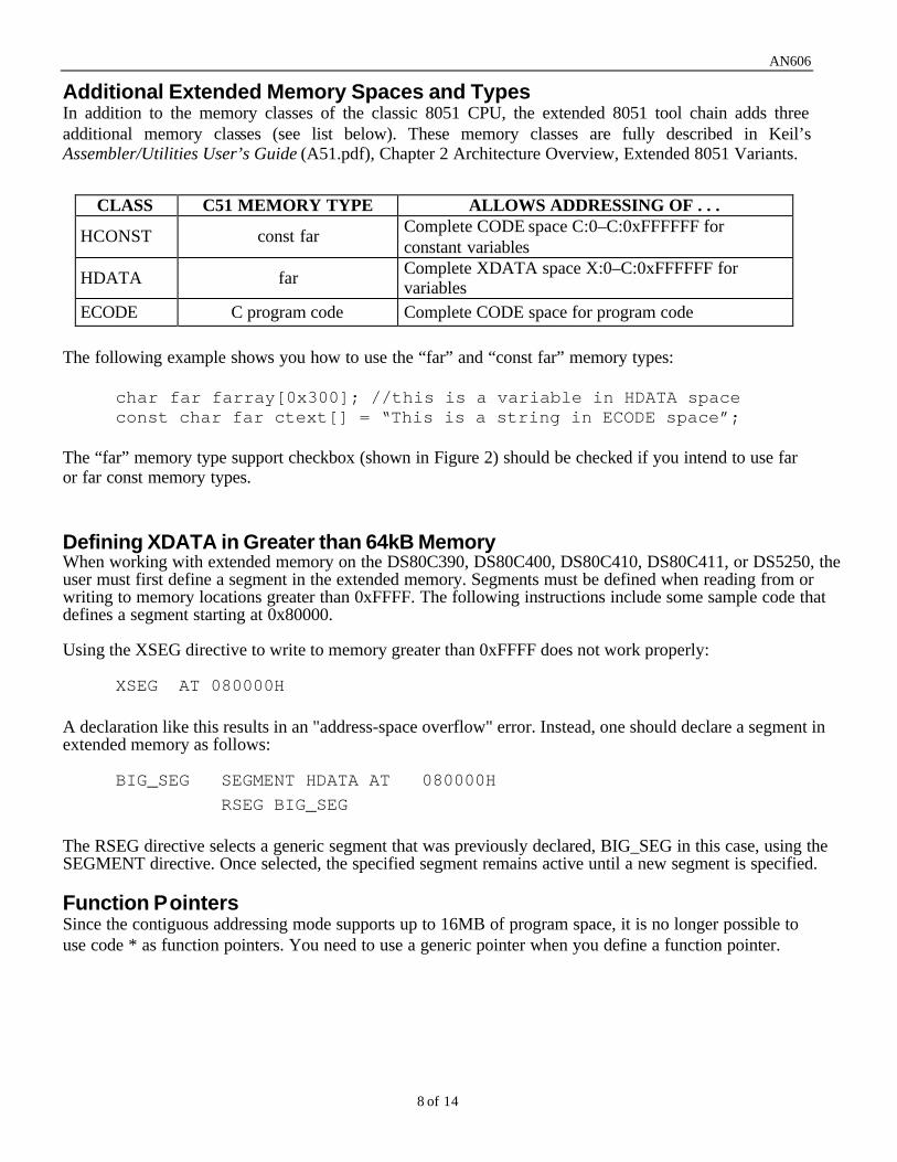
Additional Extended Memory Spaces and Types In addition to the memory classes of the classic 8051 CPU, the extended 8051 tool chain adds three additional memory classes (see list below). These memory classes are fully described in Keil’s Assembler/Utilities User’s Guide (A51.pdf), Chapter 2 Architecture Overview, Extended 8051 Variants.
CLASS C51 MEMORY TYPE ALLOWS ADDRESSING OF . . .
HCONST const far Complete CODE space C:0–C:0xFFFFFF for constant variables
HDATA far Complete XDATA space X:0–C:0xFFFFFF for variables
ECODE C program code Complete CODE space for program code The following example shows you how to use the “far” and “const far” memory types:
char far farray[0x300]; //this is a variable in HDATA space const char far ctext[] = “This is a string in ECODE space”;
The “far” memory type support checkbox (shown in Figure 2) should be checked if you intend to use far or far const memory types. Defining XDATA in Greater than 64kB Memory When working with extended memory on the DS80C390, DS80C400, DS80C410, DS80C411, or DS5250, the user must first define a segment in the extended memory. Segments must be defined when reading from or writing to memory locations greater than 0xFFFF. The following instructions include some sample code that defines a segment starting at 0x80000. Using the XSEG directive to write to memory greater than 0xFFFF does not work properly: XSEGAT080000H A declaration like this results in an "address-space overflow" error. Instead, one should declare a segment in extended memory as follows: BIG_SEG SEGMENT HDATA AT 080000H RSEG BIG_SEG The RSEG directive selects a generic segment that was previously declared, BIG_SEG in this case, using the SEGMENT directive. Once selected, the specified segment remains active until a new segment is specified.
Function Pointers Since the contiguous addressing mode supports up to 16MB of program space, it is no longer possible to use code * as function pointers. You need to use a generic pointer when you define a function pointer.
AN606
9 of 14
Example DS80C390 Memory Configuration To demonstrate the utility of the startup file constants we’ve introduced and those which were already present in Keil’s START390.A51 file, let us propose an example memory configuration for the DS80C390 microcontroller. Suppose that we wish to allow 1MB of external code space by connecting a 512k x 8 memory device to each of the chip-enable signals CE0 , 1CE . We also want to have 1.5MB of external data memory and we achieve this by connecting three 512k x 8 memories, one to each of the peripheral chip-enable signals PCE0 , PCE1, and PCE2 . Shown below is a diagram of the interconnect and the program/data memory map as determined thus far. Figure 4. EXAMPLE DS80C390 PROGRAM/DATA MEMORY INTERFACE
Figure 5. EXTERNAL PROGRAM/DATA MEMORY MAP (INTERNAL SRAM STILL AT DEFAULT ADDRESSES) In the case of the DS80C390, we must also consider the on-chip memory that is present and how/where this memory should fit into our memory map. The DS80C390 contains the following internal memory:
§ (2) 256-byte RAMs that can be used as data, message center memory for the two CAN2.0B controllers
§ (1) 1kB RAM that can be used as data, stack, program § (1) 3kB RAM that can be used as data, program
The logical address ranges for these internal RAMs are controlled by SFR bit settings and can be configured within the startup file, resulting in a startup file further tailored toward DS80C390-based projects. Once again, the START390.A51 file provided by Keil already includes constants and code to assign location and function to this internal SRAM. For this example, we will use the (2) 256-byte RAMs to support CAN activity, we will use the 1kB RAM as dedicated stack memory, and we will use the 3kB RAM exclusively as MOVX data space. We also decide to define the logical addresses of the internal RAM to a range (400000h–4011FFh) such that it does not interfere or overlap the external data memory (000000h–0FFFFFh). Shown below is the memory map that has been updated to reflect our assignments for the DS80C390 internal memory.
Assigning Values to Startup File Constants Once we’ve decided on the desired memory configuration, we can assign appropriate values to the startup file constants. Shown below are assignments for constants from the original START390.A51 file and for those which we’ve added, allowing us to effect the example DS80C390 memory map earlier specified.
SA EQU 1 ; Use 1KB stack in on-chip XDATA space IDM EQU 2 ; 2 = 4KB on-chip SRAM location X:0x400000 – X:400FFF CMA EQU 1 ; 1 = CAN0 X:0x401000 – X:0x4010FF ; CAN1 X:0x401100 – X:0x4011FF P4CNT5_3 EQU 110B ; 110B = 512kB (A18-A0 enabled) P4CNT2_0 EQU 101B ; 101B = enable CE0, CE1 P5CNT2_0 EQU 110B ; 110B = enable PCE0, PCE1, PCE2 Testing for Correct Memory Access Per Our Startup File Definition As a means to evaluate our startup file settings, we create a very simple C program (shown below) that uses the FVAR and FCVAR macros to access far XDATA and ECODE memory. This code is easily modified and can serve as a template for generating accesses to specific memory locations in order to confirm proper hardware initialization and address/chip-enable generation.
#include <REG390.H> #include <absacc.h> void main (void) { while (1) { ACC = FCVAR (unsigned char, 0x07ffff); // last address under CE0 ACC = FCVAR (unsigned char, 0x080000); // first address under CE1 ACC = FVAR (unsigned char, 0x07ffff); // last address under PCE0 ACC = FVAR (unsigned char, 0x080000); // first address under PCE1 ACC = FVAR (unsigned char, 0x0fffff); // last address under PCE1 ACC = FVAR (unsigned char, 0x100000); // first address under PCE2 //----------------------------------------------------------------------------- // FVAR macro generates a call (return addr pushed onto the hardware stack), so // the following read puts LSByte of the return address into ACC //----------------------------------------------------------------------------- ACC = FVAR(unsigned char, 0x400000); // first addr internal XRAM (stack) } } Results Using the above program, we see the following signal sequence on the oscillocope images (Figures 7 and 8) corresponding to our desired program/data memory interface.
CHIP-ENABLE ACCESS ACTIVITY CE0 accesses with PSEN\ Program fetches from low 512kB and MOVC read to 07FFFFH CE1 access with PSEN\ MOVC read to 080000H PCE0 access with RD\ MOVX access to 07FFFFH PCE1 access with RD\ MOVX access to 080000H PCE1 access with RD\ MOVX access to 0FFFFFH
PCE2 access with RD\ MOVX access to 100000H
— MOVX operation to 400000H accesses internal XRAM and can be verified by viewing the contents of ACC inside of the simulator
AN606
13 of 14
Figure 7. PROGRAM MEMORY ACCESSES USING CE0 , CE1
AN606
14 of 14
Figure 8. DATA MEMORY ACCESSES USING PCE0 , PCE1 , PCE2