Application Note AN-53 www.power.com October 2017 Active Power Factor Correction – Basics Introduction Power Factor (PF) is a measure of how a load draws power from the source. When the current phasor leads the voltage phasor, PF is leading and when the current phasor lags the voltage phasor, PF is said to be lagging. A leading or lagging PF results in transmission and distribution losses and poor utilization of source capacity. A leading or lagging power factor causes energy to be transferred back and forth between the load and the source and only a part of the energy is used for performing real work. Loads that draw a non-sinusoidal current from the source, cause distortion of the source voltage waveform and lead to performance degradation of other equipment connected on the line. Regulatory standards impose limits on the quality of current waveforms drawn by equipment in order to limit the levels of harmonic currents. Several active and passive methods can be used to shape the current drawn by power supplies to achieve compliance with the regulatory standards. This application note explains power factor correction (PFC), the associated terms that are frequently used and the various techniques used to achieve power factor correction together with their benefits and disadvantages. Regulatory requirements of EN61000 are also explained. Various active and passive techniques are discussed. The single switch Continuous Conduction Mode (CCM) boost PFC topology is an optimal solution for power factor correction over a very wide range of power levels. The CCM boost topology is discussed in detail. Operating current waveforms are presented and component selection criteria are discussed. Need for Power Factor Correction For a sinusoidal AC supply with a linear load, PF is a measure of the ratio of real power and apparent power supplied by the AC source. Real power is measured in watts and represents the energy consumed by the load to do useful work. Reactive power is the power that flows back and forth between the source and the load and is a result of the reactive nature of the load connected. Apparent power is the phasor sum of the real and reactive power. The unit of real power is watt (W) and the unit of apparent power is simply volt-amp (VA). When the reactive power is high, the AC source must supply a large apparent power to support the operation of the load which results in higher RMS current. High reactive power not only demands a higher source capacity to support the load, but also results in higher transmission losses. For a pure sinusoidal voltage and current waveform, PF is the cosine of the phase angle between the voltage and current phasors. The value of PF therefore can vary from 0 to 1 and can be leading or lagging. In situations where the power factor is lagging, PF improvement is achieved by connecting capacitor banks across the source. The resulting current from the source is in phase with the applied voltage and PF correction can be achieved. PF is therefore a figure of merit indicating how effectively energy is transmitted between the source and the load. PF RMS RMS Average Power PF Apparent Power Real Power S P V I V I cos cos VOLTAGE CURRENT # # # # U U = = = = = ^ ^ h h Figure 1 shows the power in a pure capacitive circuit. As can be seen from the figure, energy is transferred between the source and the load however the net average power transferred to the load is zero. The current flow in the interconnecting wires and any source impedance results in losses that are incurred as a result of the current flow without any useful work being performed by the energy transferred back and forth. For electrical equipment such as electrical motors, PF correction can be achieved by adding a reactive component in parallel with the load. For example, a typical induction motor is an inductive load which means it has a lagging power factor. Power factor correction can be achieved by connecting a capacitor in parallel with the induction motor. AC-DC switching power supplies with a rectifier front end draw a current waveform which is not sinusoidal. The waveform contains harmonics at frequencies higher than the fundamental frequency. This often introduces some distortion in the supply voltage waveform. On a wider scale the AC supply waveform in real life is often distorted due to the increased number of non-linear loads that are connected on the grid. Figure 1. Current Flow in a Capacitive Circuit. PI-6310-020911 -0.5 -1.0 2 4 6 8 0.5 Time Power Delivered to Load E = Voltage I = Current P = Instantaneous Power Power Returned to Source = Power Delivered to Load E, I, P Load Source V I 1.0 1.5 -1.5
Transcript
Application Note AN-53
www.power.com October 2017
Active Power Factor Correction – Basics
IntroductionPower Factor (PF) is a measure of how a load draws power from the source. When the current phasor leads the voltage phasor, PF is leading and when the current phasor lags the voltage phasor, PF is said to be lagging. A leading or lagging PF results in transmission and distribution losses and poor utilization of source capacity. A leading or lagging power factor causes energy to be transferred back and forth between the load and the source and only a part of the energy is used for performing real work. Loads that draw a non-sinusoidal current from the source, cause distortion of the source voltage waveform and lead to performance degradation of other equipment connected on the line. Regulatory standards impose limits on the quality of current waveforms drawn by equipment in order to limit the levels of harmonic currents. Several active and passive methods can be used to shape the current drawn by power supplies to achieve compliance with the regulatory standards.
This application note explains power factor correction (PFC), the associated terms that are frequently used and the various techniques used to achieve power factor correction together with their benefits and disadvantages. Regulatory requirements of EN61000 are also explained. Various active and passive techniques are discussed. The single switch Continuous Conduction Mode (CCM) boost PFC topology is an optimal solution for power factor correction over a very wide range of power levels. The CCM boost topology is discussed in detail. Operating current waveforms are presented and component selection criteria are discussed.
Need for Power Factor CorrectionFor a sinusoidal AC supply with a linear load, PF is a measure of the ratio of real power and apparent power supplied by the AC source. Real power is measured in watts and represents the energy consumed by the load to do useful work. Reactive power is the power that flows back and forth between the source and the load and is a result of the reactive nature of the load connected. Apparent power is the phasor sum of the real and reactive power. The unit of real power is watt (W) and the unit of apparent power is simply volt-amp (VA). When the reactive power is high, the AC source must supply a large apparent power to support the operation of the load which results in higher RMS current. High reactive power not only demands a higher source capacity to support the load, but also results in higher transmission losses. For a pure sinusoidal voltage and current waveform, PF is the cosine of the phase angle between the voltage and current phasors. The value of PF therefore can vary from 0 to 1 and can be leading or lagging. In situations where the power factor is lagging, PF improvement is achieved by connecting capacitor banks across the source. The resulting current from the source is in phase with the applied voltage and PF correction can be achieved. PF is therefore a figure of merit indicating how effectively energy is transmitted between the source and the load.
PFRMS RMSAverage Power
PFApparent PowerReal Power
SP
V IV I cos
cos
VOLTAGE CURRENT#
#
# # UU
=
= = = =^ ^h h
Figure 1 shows the power in a pure capacitive circuit. As can be seen from the figure, energy is transferred between the source and the load however the net average power transferred to the load is zero. The current flow in the interconnecting wires and any source impedance results in losses that are incurred as a result of the current flow without any useful work being performed by the energy transferred back and forth. For electrical equipment such as electrical motors, PF correction can be achieved by adding a reactive component in parallel with the load. For example, a typical induction motor is an inductive load which means it has a lagging power factor. Power factor correction can be achieved by connecting a capacitor in parallel with the induction motor. AC-DC switching power supplies with a rectifier front end draw a current waveform which is not sinusoidal. The waveform contains harmonics at frequencies higher than the fundamental frequency. This often introduces some distortion in the supply voltage waveform. On a wider scale the AC supply waveform in real life is often distorted due to the increased number of non-linear loads that are connected on the grid.
The AC power being transmitted to the switching power supply load now consists of power transmission at the harmonic frequencies in addition to power being supplied at the fundamental frequency. When frequency components other than the fundamental component are present in the current waveform, the total harmonic distortion (THD) of the current waveform can be calculated as:
,
,THDi
I rms
I rmsN
n
1
2=
3
=
2/
In = amplitude of nth harmonic of currentI1 = amplitude of the fundamental component of current
Total harmonic distortion of input current is a measure of departure of the current waveform from a true sine wave.
Distortion factor or Kp is calculated as:
KTHDi11
p 2=
+
Displacement Factor Kd is the cosine of the displacement between the fundamental component of the input current and the sinusoidal input voltage and is calculated as:
K cos 1 1d iU= -^ hΦ1 and q1 are the phase angles of the voltage and current phasors with respect to a reference.
When the current waveforms are non-sinusoidal and contain harmonics, power factor is calculated as:
PF K Kp d#=
Figure 2 shows the basic circuit configuration of a typical rectifier front end of a switching power supply. This rectifier circuit has a capacitor at its output which acts as a filter to convert the incoming AC supply to a low ripple DC voltage.
The resulting current waveform is pulsating in nature and contains several harmonics as shown in Figure 4. Since the pulsating waveform is symmetrical in both half-cycles, the harmonic spectrum primarily consists of odd harmonics.
The average power is now calculated using the equation:
P V I V I cos2AVN N
N N
N
0 0
1
{ i= + -3
=
^ h/
V0 and I0 = DC components of voltage and current respectively. These are mostly absent when voltage and current waveforms have complete half wave symmetryVN and IN = Amplitudes of the voltage and current harmonicsϕN and qN = Phase displacement of the voltage and current harmonics
The equation indicates that only when the voltage and current waveform contain the same harmonic, power is transferred at that harmonic frequency. If the AC supply voltage is purely sinusoidal and free of harmonics at any other frequency, the presence of harmonics in the currZZZ)ent waveform, only increases the RMS value of the current waveform and leaves the average power unchanged. Increase in the RMS value of current results in added transmission line losses.
The RMS value of the current waveform is calculated as:
rms current I INN
02 2
1
= +3
=
^ h /I0 = DC components of currentIN = amplitudes of the nth current harmonic
When the current being drawn from the source has a high harmonic content, it typically leads to distortion of the voltage waveform since a real voltage source has finite source impedance. This in turn leads to
increased losses in equipment such as motors and transformers connected on the same lines which are operating from the same distorted supply voltage.
Even if the current waveform has a high THD, it does not necessarily result in a poor PF. Figure 5 shows a trapezoidal current waveform which has high PF as there is little displace-ment between the fundamental component of current and the voltage although the current waveform has significant THD. In this example the current waveform meets Class D compliance of IEC/EN61000-3-2.
Regulatory Requirements and EN61000-3-2Current waveform distortion leads to transmission line losses and also affects performance of other equipment connected on the same distribution network. Some of these effects include defective operation of regulating devices, disturbed operation of fluorescent lamps, TV equipment, signaling systems, protective relays and telephone interference. Regulatory standards define the threshold of acceptable levels of distortion to limit the impact such waveform distortion can have on equipment connected to the line.
IEC 61000-3-2 is a standard that assesses and sets the limits for harmonic currents drawn by equipment that draw a current less than or equal to sixteen ampere per phase from the line. Distorted current waveform such as the pulsating current waveform drawn by a full wave rectifier as shown in Figure 3 consists of the fundamental component at the supply frequency and a series of harmonics which are multiples of the supply frequency. IEC61000-3-2 offers guidelines for classification of equipment depending on application and defines the permissible limit of amplitude of harmonic currents for each of the classes. Table 1 can be used to determine the class of the equipment depending on application.
Figure 5. Trapezoidal Current Waveform and Harmonic Spectrum.
Table 3. Harmonic Limits for Class C Equipment per IEC61000-3-2 for PIN >25 W (For PIN <25 W, 3rd Harmonic Amplitude Should be less than 86% of the Fundamental and 5th Harmonic Amplitude Should be less than 61% of the Fundamental).
The limits for Class A, C and D are provide in tables shown in Table 2, Table 3 and Table 4 respectively.
The notable differences between the tables shown are:1. The limits specified for Class B are 1.5 times higher than the limits
specified for Class A.2. For Class C equipment, the limits on harmonics are specified as a
percentage of the measured amplitude of the fundamental.3. Class D limits are specified in terms of mA/W of load power.4. For Class D equipment limits are specified only for odd harmonics
of current.
The standard specifies limits on the harmonic currents and does not specify permissible PF. In order to meet the Class D requirements an input power factor of 0.9 or higher is typically necessary. For applications such as lighting, there are country specific requirements that may be applicable and in some cases a PF of 0.95 or higher may be required. While the IEC61000-3-2 standard is primarily applicable in Europe, limits for PF and harmonic distortion are applicable in other parts of the world. CCC in China and JIC6100-3-2 in Japan are some examples of applicable regulatory requirements.
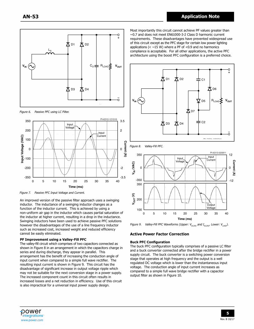
Passive PFC using an LC FilterFor a switching power supply with a rectifier front end, PF improvement can be achieved by simply incorporating an LC filter as a part of the circuit. The use of the inductor in combination with the filter capacitor has the effect of increasing the conduction angle while simultaneously reducing the peak current which results in improvement of PF. Figure 6 shows the electrical schematic of a passive PFC implementation. Although this is a simple circuit arrangement, the inductor used is a line frequency inductor which is often bulky and expensive. For power supplies that must operate over a wide operating voltage range, a tapped inductor is sometimes used with additional circuitry using relays to select the appropriate tap depending on the line voltage used. The additional losses resulting from the use of the filter inductor often prevents use of this circuit in order to meet energy efficiency requirements.
Table 1. Classification of Equipment According to IEC610000-3-2.
Table 4. Harmonic Limits for Class D Equipment per IEC610000-3-2.
Table 2. Harmonic Limits for Class A Equipment per IEC610000-3-2.
Class A • Balanced three-phase equipment• Household appliances, excluding equipment
identified by Class D• Tools excluding portable tools• Dimmers for incandescent lamps• Audio equipment• Everything else that is not classified as B, C or D
Class B • Portable tools• Arc welding equipment which is not professional
equipment
Class C • Lighting equipment
Class D • Personal computers and monitors• Television receivers• Note: Equipment must have power level 75 W
up to and not exceeding 600 W
Harmonic Order (n) Maximum PermissibleHarmonic Current (A)
Odd Harmonics
3 2.30
5 1.14
7 0.77
9 0.40
11 0.33
13 0.21
15 ≤ n ≤ 39 0.15 n15
Even Harmonics
2 1.08
4 0.43
6 0.30
8 ≤ n ≤ 40 0.23 n8
Harmonic Order (n)
Maximum PermissibleHarmonic Current Expressed as a Percentage of the Input Current at the Fundamental
An improved version of the passive filter approach uses a swinging inductor. The inductance of a swinging inductor changes as a function of the inductor current. This is achieved by using a non-uniform air gap in the inductor which causes partial saturation of the inductor at higher current, resulting in a drop in the inductance. Swinging inductors have been used to achieve passive PFC solutions however the disadvantages of the use of a line frequency inductor such as increased cost, increased weight and reduced efficiency cannot be easily eliminated.
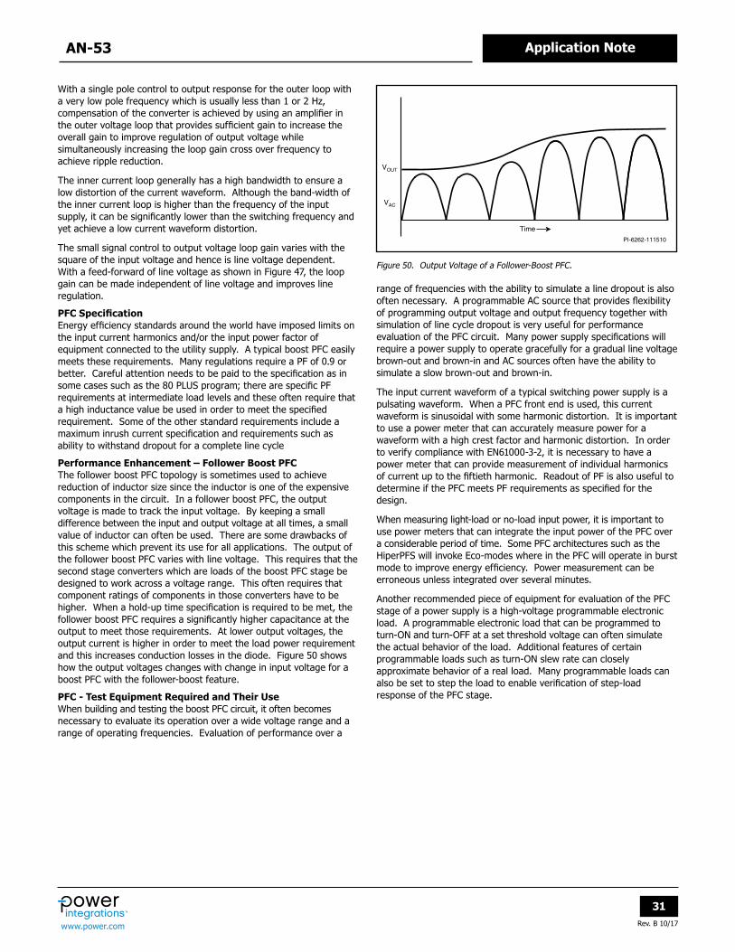
PF Improvement using a Valley-Fill PFCThe valley-fill circuit which comprises of two capacitors connected as shown in Figure 8 in an arrangement in which the capacitors charge in series and during discharge, they appear in parallel. This arrangement has the benefit of increasing the conduction angle of input current when compared to a simple full wave rectifier. The resulting input current is shown in Figure 9. This circuit has the disadvantage of significant increase in output voltage ripple which may not be suitable for the next conversion stage in a power supply. The increased component count in this circuit often results in increased losses and a net reduction in efficiency. Use of this circuit is also impractical for a universal input power supply design.
Most importantly this circuit cannot achieve PF values greater than ~0.7 and does not meet EN61000-3-2 Class D harmonic current requirements. These disadvantages have prevented widespread use of this circuit except as the PFC stage for certain low power lighting applications (< ~15 W) where a PF of <0.9 and no harmonics compliance is acceptable. For all other applications, the active PFC architecture using the boost PFC configuration is a preferred choice.
Active Power Factor Correction
Buck PFC ConfigurationThe buck PFC configuration typically comprises of a passive LC filter and a buck converter connected after the bridge rectifier in a power supply circuit. The buck converter is a switching power conversion stage that operates at high frequency and the output is a well regulated DC voltage which is lower than the instantaneous input voltage. The conduction angle of input current increases as compared to a simple full wave bridge rectifier with a capacitor output filter as shown in Figure 10.
The transfer function of a buck converter, VOUT = VIN × d (where VOUT is the output voltage, VIN is the instantaneous input voltage and d is the duty cycle of the switch), requires VOUT ≤ VIN. Since there must be minimal input capacitance (in order to achieve high power factor) the instantaneous input voltage tracks the incoming AC. To ensure that input current conduction angle is maximized requires the output voltage of the buck PFC circuit to be kept substantially lower (<50%) than the peak input voltage.
Figure 10. Buck PFC and Operating Waveforms.
A lower output voltage requires that any second conversion stage that loads the PFC must be designed to operate from that lower voltage. This results in a higher RMS currents in the second stage converter for the same power being processed, higher losses and reduced power supply efficiency.
Time period between phase angle of 0 and phase angle of α in Figure 10 (c) is the period for which the buck PFC does not draw any current from input. To minimize harmonic distortion of input current and achieve highest power factor it is necessary to minimize this period.
The lower output voltage also requires a significantly larger buck converter output capacitor to meet hold-up time specification. Should the switching element in the buck converter fail, it can result in a short-circuit between the buck converter input and output. Care has to be taken in the design to protect components at the output of the buck PFC circuit should such a fault occur.
For these reasons the buck converter is seldom used as a PFC stage.The current drawn by the buck converter is a pulsating current (vs. triangular in a boost converter) and therefore the magnitude and harmonic range of frequencies to be filtered is significantly higher. This requires physically larger components and/or additional filter stages.
Basic Boost PFC ConfigurationThe boost converter based PFC is the most popular and widely used PFC configuration. This configuration also provides the widest conduction angle for the input current and enables design of PFC circuits that can achieve low distortion input current and a PF close to 1.
The boost PFC circuit configuration is shown in Figure 11. This circuit requires one inductor, a diode and a switching element, typically a MOSFET. The output voltage of the boost converter is higher than the input. A typical boost PFC is designed such that the regulated output voltage of the converter is higher than the peak of the highest input voltage. This allows the boost PFC circuit to achieve an input current waveform that has the same shape as the input voltage waveform for most of the operating input voltage range. For a sinusoidal voltage waveform input, except for the region near the zero cross (highlighted in Figure 12), the input current waveform is also sinusoidal with only a slight distortion depending on the control technique and the inductance used. The higher output voltage often helps reduce losses in the second stage converter since it results in
lower currents. The higher operating voltage offers other benefits as well. The capacitance required for hold-up is considerably reduced since the energy stored in a capacitor goes up with the square of the voltage. A simplified block diagram of a typical multiplier based boost PFC is shown in Figure 16.
The boost converter works by storing energy in the inductor when the MOSFET is ON. During this time, the energy required by the load is supplied by the output capacitor. When the MOSFET switches OFF, polarity of the voltage across the inductor reverses causing the output diode to become forward biased and energy is transferred to the output capacitor and load. Figure 13, 14 and 15 show the basic boost converter circuit and the two operating states.
D1 D2
Power Stage Output Filter, Loadand Voltage Divider
Figure 14. Boost Converter Current Flow When the MOSFET is ON.
Figure 15. Boost Converter Current Flow When the MOSFET is OFF.
Figure 16. Simplified Block Diagram.
The duty cycle of the MOSFET operation is determined by the control technique that is used to shape the input current.
The MOSFET is typically hard switched and is switched at a high switching frequency. Switching frequencies typically range from 65 kHz to 120 kHz to minimize the size of inductor required. A low switching frequency results in lower switching losses and EMI but results in increased inductor size
A boost PFC typically has a two loop configuration in which there is an inner current loop which has a high bandwidth and an outer voltage loop that has a low bandwidth. The higher bandwidth inner current control loop ensures that the current waveform responds to line voltage changes rapidly thereby maintaining control over the shape of the current waveform. The slow outer voltage loop ensures that the average output voltage is constant while ensuring that the outer loop does not interfere with the operation of the inner current control loop.
The slow outer voltage loop can results in overshoot of output voltage during transient load conditions and often requires additional circuitry or functional blocks inside the controller to quickly respond to transient conditions to limit any overshoot of output voltage.
In a traditional multiplier based PFC shown in Figure 16, the voltage at the output of the input bridge rectifier serves as a reference to the current control amplifier. The amplitude of the reference is the product of the amplitude of the voltage waveform sensed after the bridge rectifier and the output of the error amplifier that senses the PFC output voltage.
PI-6224-110810
DL
C RLOAD VOUTVIN
+PWM
CONTROL
++
PI-6236-110810
L
C
D
RLOADVOUTVIN
SwitchON
++
PI-6237-110810
L
C
D
RLOADVOUTVIN
SwitchOFF
++
D1 D2
Power Stage Output Filter, Loadand Voltage Divider
Figure 17. DCM (a), CRM (b) and CCM (c) Operation – Input Current Waveforms.
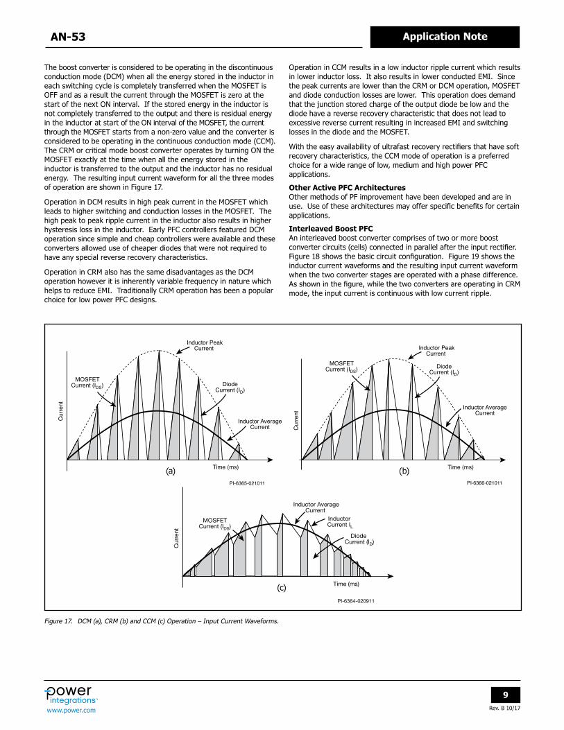
The boost converter is considered to be operating in the discontinuous conduction mode (DCM) when all the energy stored in the inductor in each switching cycle is completely transferred when the MOSFET is OFF and as a result the current through the MOSFET is zero at the start of the next ON interval. If the stored energy in the inductor is not completely transferred to the output and there is residual energy in the inductor at start of the ON interval of the MOSFET, the current through the MOSFET starts from a non-zero value and the converter is considered to be operating in the continuous conduction mode (CCM). The CRM or critical mode boost converter operates by turning ON the MOSFET exactly at the time when all the energy stored in the inductor is transferred to the output and the inductor has no residual energy. The resulting input current waveform for all the three modes of operation are shown in Figure 17.
Operation in DCM results in high peak current in the MOSFET which leads to higher switching and conduction losses in the MOSFET. The high peak to peak ripple current in the inductor also results in higher hysteresis loss in the inductor. Early PFC controllers featured DCM operation since simple and cheap controllers were available and these converters allowed use of cheaper diodes that were not required to have any special reverse recovery characteristics.
Operation in CRM also has the same disadvantages as the DCM operation however it is inherently variable frequency in nature which helps to reduce EMI. Traditionally CRM operation has been a popular choice for low power PFC designs.
Operation in CCM results in a low inductor ripple current which results in lower inductor loss. It also results in lower conducted EMI. Since the peak currents are lower than the CRM or DCM operation, MOSFET and diode conduction losses are lower. This operation does demand that the junction stored charge of the output diode be low and the diode have a reverse recovery characteristic that does not lead to excessive reverse current resulting in increased EMI and switching losses in the diode and the MOSFET.
With the easy availability of ultrafast recovery rectifiers that have soft recovery characteristics, the CCM mode of operation is a preferred choice for a wide range of low, medium and high power PFC applications.
Other Active PFC ArchitecturesOther methods of PF improvement have been developed and are in use. Use of these architectures may offer specific benefits for certain applications.
Interleaved Boost PFCAn interleaved boost converter comprises of two or more boost converter circuits (cells) connected in parallel after the input rectifier. Figure 18 shows the basic circuit configuration. Figure 19 shows the inductor current waveforms and the resulting input current waveform when the two converter stages are operated with a phase difference. As shown in the figure, while the two converters are operating in CRM mode, the input current is continuous with low current ripple.
The interleaved boost topology can be suitably modified to turn-ON and turn-OFF the boost conversion stages to optimize operating efficiency across load range. A number of variations of control scheme are possible which includes selectively operating specific cells in CCM, DCM or CRM mode to optimize operating efficiency at different load levels. With the power being distributed over multiple boost conversion cells, losses are distributed over multiple components which can be an advantage for thermal design.
Figure 19. Inductor Current and Input Current Waveforms in an Interleaved Converter with CRM Operation.
Figure 18. Interleaved Boost PFC Converter.
VOUTVIN
BR1 D1
D2L2
L1
Q2Q1 C1 RLOAD
RS
PI-6225-020811
+
PI-6226-020811
Indu
ctor
Cur
rent
s
S = Slope of Inductor Current
2SON
ResultingInput Current IL1 + IL2
SON
IL2IL1
TSW/2 TSW/2time
(1-D)TSW(D-0.5)TSW
ΔI
SON
t
ILPK
Although this arrangement enables CRM switching and load sharing among converter stages while using a common input rectifier and output filter, there is a significant increase in the total number of components used. This scheme offers some advantage at significantly high power levels and the increase in component count has prevented its use in medium and low power applications.
Flyback Power Supply with Integrated PFCThere are a number of flyback power supply variations in use that have high input power factor. Flyback converters with or without an input filter capacitor have been designed with control techniques than enable a low distortion input waveshape with high PF. Figure 20 shows one such scheme that utilizes charge control. Use of a flyback converter provides input to output isolation and output voltage can be either higher or lower than the input since it is determined by the turns ratio of the transformer.
The flyback PFC has been used successfully for low power (<~70 W) applications. The flyback PFC has not proven to be cost effective or as energy efficient at medium and high power levels. When used as a single stage converter (the load is directly connected to the output rather than to a second conversion stage) it has the downside of requiring a large output capacitor. This has to provide energy storage at line frequency, therefore requiring much larger capacitance value to give low output voltage ripple.
The integrated flyback PFC configuration is a popular choice for LED lighting solutions as significant output ripple is generally acceptable reducing the output capacitance required. With the use of innovative control techniques, flyback converters operating either in DCM or CCM can be made to operate with duty cycle modulation that automatically shapes the input current and results in a high PF.
Selection Criteria for Boost-PFC configurationsCCM boost PFC configuration is the most optimal circuit configuration for a wide range of applications. Table 5 high-lights the relative differences between the CCM, CRM and the DCM PFC configurations.
Power Integrations offers HiperPFS, HiperPLC and the LinkSwitch-PH products that feature a CCM PFC technique. The HiperPFS is an integrated power IC which integrates a MOSFET, its associated drive circuit, required control circuit with built in current sense circuitry results in a highly integrated solution for PFC applications.
Table 5. Relative Comparison of CCM, DCM and CRM PFC Options ( H = High, L = Low, Y = Yes).
AN-52 provides details of the HiperPFS product and guidelines for design of a PFC using HiperPFS.
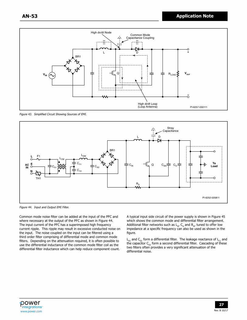
Functional Blocks of a Boost PFC ConverterA typical boost PFC converter stage comprises of an EMI filter, a bridge rectifier, a boost converter with an output filter capacitor and additional components required for circuit protection such as a fuse, a varistor if necessary and any inrush current limiting circuitry or thermistors.
A schematic showing the basic components of a boost PFC using the HiperPFS integrated PFC controller is shown in Figure 21. This circuit shows a fuse at the input. The fuse safely isolates the circuit from the source in case of an overload fault at the output of the boost converter or in case of failure of any of the components in the circuit that results in an input current in excess of the fuse rating. The inrush limiters (thermistors) limit the input current during a start-up to a level that prevents failure of any of the components used. The EMI filter circuit which comprises of a differential mode and a common mode EMI filter limits the switching noise coupled into the AC source. The bridge rectifier BR1 rectifies the input AC into DC. The circuit comprising of inductor L1, MOSFET within U1 and diode D1 work as a boost converter. The control circuit senses the output voltage and adjusts the duty cycle of MOSFET operation so as to
regulate the output voltage. The output voltage feedback and compensation circuit scale the output voltage to a low value suitable for the controller and provides loop compensation for stable operation. In case of a HiperPFS device, the controller and MOSFET are integrated including MOSFET current sensing. Additional capacitors are shown in the circuit which can be used to reduce EMI. The capacitors are shown across the output diode D1 and from the cathode of the output diode D1 to the DC return. Use of these capacitors helps in controlling dv/dt during switch transitions. The capacitor connected from the cathode of the output diode to the DC return helps in reducing the loop area of the output circuit.
An inrush bypass diode (D2) is shown in the circuit. This diode is necessary to ensure that the output capacitor of the boost PFC is pre charged to the peak of the input voltage at start and the charging current is routed through the diode D2 instead of the inductor L1 and diode D1. In the absence of this diode, the inrush current would flow through the inductor L1, resulting in a build-up of voltage at the output due to the resonance between the output capacitor and the inductor L1. In the absence of any load at output, this voltage could be twice the peak of the applied input voltage which in most circuits will lead to failure of the output capacitor or the internal MOSFET of U1.
Figure 21. Boost PFC Basic Schematic.
BR1
L1 D1
D2
*Alternate location for thermistor**Not required for all designs
Operation of a Boost ConverterThe boost converter operating waveforms are shown in Figure 22. A switching cycle starts with the MOSFET Q1 being turned ON. The drain-source voltage across the MOSFET drops to a low level and corresponds to the product of the RDS(ON) of the MOSFET and the current through the drain. The output diode D1 is reverse biased and is in a blocking state when the MOSFET is ON. The current through the inductor rises linearly until the MOSFET is switched OFF. Once the MOSFET turns-OFF, polarity reversal of the inductor causes the inductor current to commutate to the output diode. The voltage drop across the output diode is the forward drop of the diode due to the current flowing through the diode. The drain-source voltage across the MOSFET is the sum of the output voltage across capacitor COUT and the diode drop.
The gray colored waveforms shown in the figure are for CCM operation and the black colored waveforms are for the CRM operation. Since the inductor current is not zero at the instant of turn-ON of the MOSFET, the output diode undergoes reverse recovery as it goes from a conducting to a non-conducting state which results
in a spike of current through the MOSFET and the diode as shown in the Figure 22. In practice it is important to limit the amplitude of this spike for limiting switching losses without exceeding specified device limits. This spike can also lead to increased EMI since this spike of current has a short duration and high amplitude with a fast transition.
The energy transfer from the input to the output is pulsating in nature. When the MOSFET is ON, storing energy in the inductor, the output load current is supplied from the output capacitor. A sufficiently large output capacitor is required to ensure that the output ripple voltage is a small fraction of the average output voltage. The energy stored in the output capacitor also supports the load during a line dropout, typically for durations lasting from a fraction of a cycle to a complete cycle or more, depending on the size of the capacitor.
For a boost converter the output voltage is determined by the duty cycle of operation of the MOSFET. The duty cycle is controlled by the controller so as to regulate the output voltage.
Figure 25. MOSFET Current for a CCM – Boost Converter.
Components of a Boost PFC Converter
InductorThe inductor in a boost PFC converter stores energy when the MOSFET is ON. For a CCM operation, only a part of the stored energy is transferred to the output when the MOSFET turns OFF. For a DCM or CRM operation, all the stored energy in the inductor is transferred to the output when the MOSFET is OFF. When the MOSFET is ON, the value of the inductor determines the di/dt depending on the instantaneous input voltage. For a sinusoidal input voltage, the input changes continuously. The factor KP, which is a ratio of the ripple in the inductor current to the peak inductor current as shown in Figure 25, changes continuously. For a CCM PFC, the value of KP should be kept low in order to achieve a low distortion input current waveform. Often this value may have to be reduced further to meet specific requirements of a high power factor when operating at light-load levels.
For a converter operating in CCM, the duty cycle for any switching instant can be determined using the equation:
DV
V VO
O IN= -
The minimum inductor value required can be calculated using the equation:
LF I
V D2( )MIN
S
MIN PK
#
# #
D=
VO = PFC output voltage (V)VIN = Instantaneous PFC input voltage (V)VMIN(PK) = Peak value of low line input voltage (V)ΔI = Peak-to-peak ripple current (A)FS = Switching frequency (Hz)D = Duty cycle
The equation above shows that the inductance value required is higher for a lower value of inductor ripple current.
The losses in a boost PFC inductor consist of core loss and copper loss. The core loss is directly dependent on the ripple current in the inductor. The core loss in a CCM PFC inductor is small and is significantly lower than the copper loss. The copper loss is due to the resistance of the wire used coupled with any skin or proximity effects experienced by the winding.
A variety of core material options are available for PFC inductor. Table 6 shows a relative comparison between different core materials. Although ferrite cores are preferred for the highest efficiency PFC designs, these cores are required to be gapped to achieve the required inductance. The presence of air gap has other effects which are undesirable such as increased winding loss due to fringing fields in the air gap and increased EMI due to fringing fields coupling into filter components. Cores made from metal alloy powders that are bound with a suitable binder, offer a distributed air gap and are preferred for boost PFC inductor design. The particles of the material used are coated with insulating material and the powder is molded and sintered to the required shape. The cores are often coated with a protective coating and are color coded or marked suitably. The insulation of the individual particles results in low eddy current loss and the absence of a localized air gap eliminates the effect of fringing fields.
Table 6. Comparison of Core Materials for PFC Inductor.
Table 7. Core Materials and Applications.
Toroidal cores are the most common shape of powder cores although these cores are also available as EE cores.
Due to the distributed air gap, the saturation characteristic of the powder cores is fairly soft. This is particularly helpful under fault conditions. An abrupt saturation of the core leads to a rapid increase in current which significantly increases the stress in the MOSFET and can be damaging. Table 7 compares core materials for different applications.
Inductor DesignThe physical size of the inductor is a function of the energy required to be stored in the inductor. The energy stored in an inductor is dependent on its value (L) and peak current squared (IPK). The first step in design of the inductor for a boost PFC is determination of the inductance value. Once the required inductance is calculated, the required core size can be determined using the area product (AP) approach.
10A
BL I
J KI ( )
PPK
P PK
MAX U
IN RMS
4
##
# #= -; E
AP = Area product (cm4) LP = Inductance (H)IPK = Peak current through the inductor (A)BPK = Peak flux density (T)IIN(RMS) = RMS current through the inductor (A)JMAX = Current density (A/cm2)KU = Window utilization factor (generally 0.4)
JMAX will depend on the type of cooling usedNormally – 400 A/cm2 for convection cooled design.Up to 800 A/cm2 for forced air cooled design.
Once the core is selected for the application, the number of turns can be calculated:
10NA BL I
C PK
P PK4
#
# #=
LP = Inductance (H)AC = Core cross sectional area (cm2)IPK = Peak current through the inductor (A)BPK = Peak flux density (T)
The required air gap is calculated using the inductance. Generally the air gap is confined to the central leg of an EE core. The air gap in a core results in fringing fields around the gap which not only result in higher losses in the conductors in the immediate vicinity but also in increased EMI. In an inductor, energy is stored in the air gap. This air gap (LG) is calculated using the equation:
0.4 10LLN A
GP
C2 8
# # # #r=-
LG = Gap length (cm) LP = Inductance (H)AC = Core cross sectional area (cm2)N = Number of turns
Material Property Iron BaseAmorphous Ferrite Powdered Iron Sendust
Saturation Soft Hard Soft Soft
BTYP -0.5 Tesla < 0.28 Tesla -0.5 Tesla -0.5 Tesla
BSAT
Not temperature dependent
Temperature dependentNot temperature
dependentNot temperature
dependent
Loss Amplitude Medium Lowest Highest Medium
LossNot temperature
dependentTemperature dependent
Not temperature dependent
Not temperature dependent
Gap Distributed Physical Distributed Distributed
Core Type Core Material Price Applications
Boost PFC Inductor Line Filter High-Frequency
Energy Circuits Filter Chokes Precision Filters
Moly Permalloy
2% Molybdenum, 81% Nickel, 17% Iron
High Good Poor Poor Best Best
Sendust6% Aluminum,
9% Silicon, 85% Iron
Low Fair Good Fair Good Fair
High-Flux50% Nickel, 50% Iron
Medium Poor Best Best Worst Worst
Powdered Iron 100% Iron Lowest Worst Fair Good Worst Worst
Air gaps are generally confined to only the center limb of the core for geometries such as the EE, PQ and ETD. Large air gaps should be avoided since the fringing field in the air gap often results in increased proximity losses in the conductors adjacent to the air gap. The nature of the fringing fields is shown in Figure 26. Air gaps are often a source of radiated EMI and when the gap in placed in the center leg, vs. the outer core legs, the windings around the air gap act as a shield against radiated EMI.
Once the air gap and the number of turns are calculated, the wire size can be selected based on the available window area for winding the turns. To keep losses due to the wire resistance low, a wire of suitable diameter is selected. The equation below calculates the permissible wire size on the basis of the available window area:
AN
W KW
A U#=
AW = Wire cross sectional area (cm2)WA = Window area (cm2)N = Number of turnsKU = Window utilization factor (generally 0.4)
Inductor LossesCopper loss is the dominant loss in a CCM PFC inductor especially for very low current ripple in the inductor. A low current ripple also results in a small AC flux on the core. Since the core loss is a function of the AC component of flux swing, a small AC component of flux results in a small hysteresis loss. This loss is much smaller than the winding loss due to the DC resistance of the copper wire used.
Figure 26. Fringing Fields in an Air Gap.
The copper loss due to the DC resistance of the wire used can be calculated using the equation below:
P I MLT N R( )CU IN RMS CU2# # #=
PCU = Copper loss (W)IIN(RMS) = RMS input current (A)MLT = Mean length of each turn (cm)N = Number of turnsRCU = Resistance of the copper wire per cm
The temperature rise of an inductor is dependent on the power dissipated in the inductor and the surface area of the inductor. A relationship between the surface area and the expected temperature rise is provided in the equation below. The equation provides a result that is approximate. In real life this temperature rise depends on other factors including shape, air flow around the inductor, number of layers of winding etc.
TAP450
.
RT
CU0 826
#c c mPCU = Copper loss (W)AT = Surface area (cm2)TR = Temperature rise (°C)
Inductor Core Selection and Calculation of Turns for Powder Core InductorsWhen using a powder core, it is often easier to select a core using graphs provided in the manufacturer’s catalogs. The manufacturer’s catalogs provide graphs that make it easier to select cores based on the energy stored in the core. The equation used for calculating the LI2 product required for the application is shown below:
mH amp L IPK2 2
#- =
L = Required inductance (mH)IPK = Peak inductor current (A)
Once a core is selected, the number of turns can be calculated based on the inductance factor or the AL value of a given core as:
1000NALL
#=
L = Required inductance (mH)AL = Core nominal inductance in mH per 1000 turn
Often this calculation is required to be iterated as the AL value changes as a function of the DC bias of the core. Other sophisticated methods such as closed form solutions based on equations that account for AL value reduction can be employed if the characteristic of permeability vs. DC bias relationship is known for a core.
Figure 27. Winding with Low Parasitic Capacitance.
Figure 28. Winding with High Parasitic Capacitance.
Figure 29. Single Layer Winding. Figure 30. Multi Layer Winding. Figure 31. Z-Winding.
Winding and ConstructionIt is recommended that the number of layers on a toroidal inductor be limited to two or three. A greater number of layers, result in an increase in winding capacitance. A greater build-up of layers also has the effect of increasing the hotspot temperature of the winding.
High parasitic capacitance will lead to a high initial current in the MOSFET at turn-ON and will result in increased switching losses.
When designing the circuit board and the inductor, it is important to reduce the loop area of circuits carrying high frequency switching currents in order to reduce the signal strength of the noise signals that can couple into adjacent circuits and components resulting in EMI. When designing an inductor, a winding technique called the Z-winding can help reduce this area in the inductor. Figure 31 shows the winding technique and the resulting reduction in the loop area. A multi-layer winding shown in Figure 30 leads to a higher winding capacitance and also does not result in reduction of loop area.
Wire SelectionFor a PFC operating in CCM, single strand magnet wires can be used for inductor construction. If the operation is CRM or DCM or CCM with a significant ripple current in the inductor, losses due to skin effect and proximity effect need to be carefully considered.
When selecting wire size for inductor construction, operating current densities as high as 400 A/cm2 are typically used for designs without forced air cooling. For forced air cooled designs, current densities as high as 600 A/cm2 are often used.
Magnetic fields exist in and around a conductor carrying current. The field is radially symmetrical only if the return current with its associated field is at a great distance. At low frequencies, the current distributes itself uniformly in a wire. At high frequencies, the rapidly changing flux introduces eddy currents inside the conductor which results in a reinforced current flow along the wire surface and opposes current flow at the center.
As the frequency rises, current density rises at the conductor surface and decreases towards the centre. Since only a small portion of the conductor carries current at high frequencies, the effective wire resistance at high frequencies is much higher than the wire resistance at low frequencies.
Penetration depth or skin depth is the depth from the surface of the conductor where current density is approximately 36% of the current density at the surface. It is therefore a common practice to restrict wire size to wires that have radius equal to the skin depth at the
frequency of operation. If the wire size is too small to meet the current density requirement, multiple strands of wire are used in parallel or Litz wires are used.
Skin depth d is defined as:
f# #d
r nt
=
Where ρ is the resistivity, m is the premeability and ƒ is the frequency.
At 100 °C, the skin depth d for a copper conductor is:
.fcm7 5d =
In a multi layer winding, the layer resistance can be calculated using the equation:
cosh cossinh sin
cosh cossinh sinR v
v vv v m
v vv v R
22 1( )AC M DC
2# #=
-+ + -
+-^ h8 B
Where v is
v hd
=
And h is the layer thickness. m is the layer number.
When conductors are wound adjacent to each other, the magnetic fields generated by the conductors get added vectorially. As a result of this addition, the current in the conductor redistributes itself and crowds in an even smaller part of the conductor. In a multi layer construction, the situation becomes acute as a result of progressive buildup of the field and the eddy current loss in the wire goes up exponentially. It is for the same reason that just paralleling of conductors at high frequencies often does not yield the intended benefit. This problem can be reduced significantly through use of Litz wires.
Litz wire is a special type of wire construction made out of large number of fine wires woven together in a way that each wire successively occupies the same position within the field. The woven structure can however result in voids in the construction and result in poor utilization of the available winding window as compared to a single conductor of the same effective cross sectional area.
Boost PFC MOSFETThe MOSFET is the most optimal choice as a switching element for a boost PFC converter due to the simplicity associated with the drive design, low drive power requirement and lower losses due to their fast turn-ON and turn-OFF. IGBTs are also used at power levels that typically exceed 1 kW. The BJT is rarely used for this application.
MOSFET’s capable of blocking a voltage higher than the output voltage and with the ability to handle transient operating currents above the steady state value are required for the boost PFC application.
Switching losses of the MOSFET and other elements of the circuit increase with increase in the switching frequency. The required inductance reduces with an increase in switching frequency. The
choice of switching frequency is a compromise between switching losses and the resulting efficiency impact vs. the reduction in inductance achieved.
Zero Voltage Switching (ZVS) techniques can help reduce switching losses and thereby enable operation at higher switching frequencies. Use of ZVS/ZCS (Zero Current Switching) techniques requires use of additional components and result in increased component count and cost. The hard switched CCM PFC is therefore the topology of choice especially at power levels below 1 kW.
There are four different losses incurred in the MOSFET due to the switching at high frequency. Figure 32 shows the switching waveforms for CCM operation:
A. MOSFET turn-ON lossB. MOSFET turn-OFF lossC. MOSFET conduction lossD. Loss due to reverse recovery of output diode
The MOSFET’s instantaneous drain-source voltage (VDS) and drain current (IDS) waveforms are illustrated in the third waveform of Figure 32. The MOSFET’s turn-ON commutation is shown first followed by the turn-OFF sequence. The corresponding turn-ON and turn-OFF switching energy losses (PQ) in the MOSFET is shown in the last waveform. With reference to these waveforms, a detailed description of the MOSFET’s switching sequence is given below. The MOSFET turn-ON switching losses begin at t0, the start of drain current flow, and continue through t3. After this, conduction losses begin. MOSFET turn-ON switching losses typically account for 30% of the total power losses of a PFC circuit. The period t0 through t1 is the time required for the inductor current to be commutated from the boost diode to the MOSFET. The amount of energy loss during this period is considerable because the drain current is increasing while the drain-source voltage remains high. The time required to make this transition is controlled by the MOSFET and drive circuit characteristics. Another consideration is that the faster the MOSFET turns-ON, the snappier the boost diode’s recovery characteristic becomes. A point is reached where the snappiness causes excessive ringing and will increase the EMI generated.
The period t1 through t2 is the time required for the diode reverse recovery current to reach its peak value, IRRM. The amount of energy loss during this period is even higher because the current continues to increase and the drain-source voltage is still high. The time required to make this transition and the peak current reached, is controlled by the boost diode’s recovery characteristics. The period t2 through t3 is the time required for the diode reverse recovery current to decrease from its peak value to zero. The amount of energy loss during this period is still high but is decreasing, since in-spite of the drain current remaining high the drain source voltage is high but falling rapidly to the MOSFET’s on-state voltage. A portion of this loss is the result of the boost diode’s recovery characteristics. The period t3 through t4 is the time when the MOSFET remain in the on-state. Energy lost during this state would completely depend on the MOSFET’s RDS(ON).Using low RDS(ON) devices could result in negligible conduction losses.
Figure 32. MOSFET Switching Cycle in CCM Operation.
The MOSFET’s turn-OFF switching losses begin at t5, the point where the drain-source voltage begins to increase, and continues through t7, where the drain current reaches zero. MOSFET turn-OFF switching losses are influenced by its turn-OFF switching time and not by the boost diode characteristics. This can be mitigated by proper gate drive design and using new generation MOSFETs that have low gate charge requirements. MOSFET turn-OFF switching losses for the figure shown as an example here, account for 13% of the total power losses. Thus the simplest way to reduce the MOSFET’s turn-OFF switching energy losses would be to switch at a faster speed. This of course is true only to a point. The faster the boost diode is forced to recover, the higher the peak recovery current becomes, negating some of the switching loss savings.
For a DCM/CRM operation, the inductor current and hence the output diode current is zero at start of the cycle. This eliminates losses associated with reverse recovery of the diode and the turn-ON loss due to commutation of the current from the diode to the MOSFET since the current starts from zero.
The MOSFET conduction loss is due to the RDS(ON) of the MOSFET. RDS(ON) of the MOSFET increases with temperature. For an accurate estimation, it is necessary that the value of RDS(ON) used corresponds to the temperature of the MOSFET junction.
Conduction loss can be calculated using the equation below:
P I R ( )CON D DS HOT2#=
ID = MOSFET RMS Drain Current (A)RDS(HOT) = RDS(ON) of the MOSFET when the MOSFET is hot
The switching loss of the MOSFET, which comprises of turn-ON and turn-OFF loss and also additional power loss due to discharge of the MOSFET capacitance COSS, each time the MOSFET turns-ON. This loss can be calculated for each cycle using the equation below:
P I V t t C Vf f21
21
SW D D OFF ON SW OSS D SW2
# # # # # #= + +^ htOFF = Turn-OFF time of the MOSFETtON = Turn-ON time of the MOSFETfSW = Switching frequency of the PFCID = MOSFET Drain CurrentVD = MOSFET Drain Source voltage just after MOSFET turn-OFF (typically equals VO)COSS = MOSFET output capacitance
Each time the MOSFET turns-ON when the converter operates in CCM, a reverse current flows through the output diode during its recovery from the forward conducting state. This current flows through the MOSFET as it is turning ON. This leads to additional losses in the MOSFET which can be calculated using the equation:
P V Q fRR O RR S# #=
QRR = Reverse recovery charge of the diodeVO = PFC output voltagefS = PFC operating frequency
The value of QRR is dependent on the diode forward current prior to turn-OFF and the di/dt during turn off of the diode. Since these parameters are difficult to determine based on the limited information provided in most diode data sheets, this loss is often difficult to calculate accurately.
Each time the MOSFET is turned ON and OFF, power is dissipated in the gate drive circuit. Power supplied by the VCC supply can be calculated using the equation
P Q V fGATE G CC SW# #=
QG = Total gate charge (C)VCC = Driver supply voltage (V)fSW = MOSFET switching frequency (Hz)
PFC Output DiodeIn case of a boost PFC, when the MOSFET switches OFF, inductor current commutates to the output diode as shown in Figure 22. Energy is transferred to the output when the diode conducts. The conduction loss of the diode is a function of the diode forward drop.
For a CCM boost converter, the diode goes from a conducting state to a reverse blocking state when the MOSFET turns ON. For the hard switched CCM boost converter, this transition from the conducting to the reverse blocking state is abrupt. The minority carriers in the space charge region return to the respective p or n region. The resulting shape of the reverse current and its magnitude can be significantly different in different diodes depending on the fabrication.
Types of DiodesDiodes are classified depending on their characteristics as standard recovery, fast recovery and ultrafast recovery diodes. Tandem diodes, special high frequency diodes and SiC Schottky diodes are all ultrafast diodes and are discussed here since these diodes are invariably used for CCM PFC application.
Standard Recovery DiodesStandard recovery diodes are used for rectification of low frequency waveforms such as the input voltage of a power supply operating from a 50 Hz / 60 Hz AC line. Standard recovery silicon diodes have reverse recovery times of 1 ms or higher and are not suitable for the hard switched CCM PFC output diode application. These diodes are used in the input bridge rectifier as the input voltage of the PFC is typically line frequency which is low frequency (50/60 Hz).
Fast Recovery DiodesFast recovery diodes are typically silicon diodes that exhibit superior reverse recovery characteristics as compared to the standard recovery diodes. Typical recovery times range from 200 ns to 500 ns. For a hard switched CCM PFC, the MOSFET turn-ON time is reduced to limit MOSFET switching losses. These turn ON times are typically in the region of 30 ns to 100 ns and these diodes are therefore not suitable as PFC output diodes. The use of these diodes in high switching frequency circuits is limited to circuits where other means to control the reverse current are employed
Ultrafast DiodesThese diodes typically have reverse recovery times less than 100 ns. The fast switching of these diodes permits their use in hard switched applications where the turn-ON and turn-OFF times are often less than 100 ns.
Tandem DiodesLow voltage ultrafast diodes have a much lower reverse recovery time as compared to the high-voltage ultrafast diodes. Often manufacturers sort the dice in production and combine matching dice in a single package which are series connected. The resulting diode has superior reverse recovery characteristic with low recovery time thought the forward drop of such a part is higher.
Special High Frequency Diodes (PFC Specific Diodes)PFC specific diodes are offered by a number of manufacturers. These diodes feature a recovery characteristic which is fast as well as soft in nature. Unlike many ultrafast diodes that have a snappy reverse recovery, the recovery characteristic of these diodes is soft which reduces EMI while limiting switching losses. A diode’s softness rating (S), is defined as ratio of the time required for the recovery current to become zero from its maximum to the time required for the recovery current to reach this maximum value during its turn-OFF. These PFC specific diodes have a softness values greater than 1.2 and have a reverse recovery time of less than 35 ns. This softness allows Figure 33. Diode Softness Factor Definition.
monotonic current recovery reducing EMI. The forward drop and the cost of these diodes are lower than single package series connected diodes (tandem diodes).
Figure 34 shows a comparison of reverse recovery characteristics of Power Integrations Qspeed (H-Series, Q-Series, X-Series) with tandem and ultrafast diodes.
Silicon Carbide DiodesThe SiC Schottky diodes has superior switching characteristics over leading ultrafast recovery diodes. There are minimal switching losses in the SiC Schottky diodes compared to ultrafast recovery diodes. The switching losses of the SiC Schottky diodes increase slightly with an increase in diode peak current compared to a considerable increase in switching losses of the ultrafast recovery diodes. The availability of SiC Schottky diodes with high blocking voltages makes them a suitable device for PFC applications with higher operating frequency and increased power density. These devices do not have any reverse recovery current. During switching transitions, only a small reverse current flows due to the junction capacitance of these diodes. This junction charge is much lower than QRR for silicon ultrafast diodes. Unlike a silicon ultrafast diode, the switching losses are independent of forward current, di/dt or temperature. The positive temperature coefficient of these diodes eases paralleling without risk. These devices are often expensive and that limits their use to high density / high performance power supplies.
Softness Factor – Diode Reverse RecoverySoftness factor “S” is the measure of recovery softness for a diode. Figure 33 shows the general nature of reverse recovery current as the diode recovers and how the softness factor is calculated. It is possible that a diode has a low tRR but has a high QRR which results in higher switching losses in the MOSFET. QRR therefore is a better measure of diode quality.
Figure 34. Comparison of QRR for H-Series, Q-Series, X-Series, Tandem, and an Ultrafast Diode.
Figure 35. Diode Recovery Forward.
It is important to compare the softness factor, tRR and QRR of diodes in order to assess the overall benefit of a particular diode selection. Figure 34 shows that although some ultrafast diodes have extremely low tRR, their abrupt recovery causes ringing in the current waveform that can lead to higher EMI.
It is often found that diode data sheets have insufficiency information regarding the reverse recovery characteristics. When using such diodes, it is advisable to seek more information prior to their use to ensure that the diode is suitable for the application.
Diode Forward RecoveryWhen the MOSFET turns-OFF, current is commutated to the diode. In a hard switched CCM PFC, this transition is extremely fast in order to reduce switching losses in the MOSFET. As the current commutates to the diode, the diode undergoes a phenomenon called forward recovery. During forward recovery, the voltage drop across the diode is much higher than the expected diode drop. This is primarily caused by the lead and parasitic inductances. Figure 35 shows the typical forward recovery characteristic of a diode in a hard switched CCM PFC application. VFP or the peak forward voltage can be as high as 12 V. The sum total of diode forward voltage during forward recovery, voltage drops in the circuit parasitic impedances and the output voltage is the voltage that will appear across the MOSFET at the instant of turn-OFF. The forward recovery characteristic therefore determines the voltage level across the MOSFET during turn-OFF.
Forward recovery parameters are often unspecified for most diodes as it was not a standard requirement for JEDEC registered diodes.
Diode LossesConduction loss occurs in the PFC output diode due to the current that flows through the diode in each cycle. This loss is directly dependent on the diode forward current and the diode operating temperature. Switching losses occur in the diode each time the diode transitions between the forward conducting state and the reverse blocking state. Diode losses for the PFC output diode can be estimated using the equations provided below.
Conduction loss for a diode can be estimated using the following equation. A diode voltage drop VF corresponding to the RMS diode current should be used for this calculation.
Diode Conduction LossApproximate diode RMS current for a given operating condition can be calculated using the equation
316I
VP
VV
2( )D RMS
O
O
IN
O#
# # #
#
r=
VO = PFC output voltage (V)PO = PFC output power (W)VIN = PFC AC input RMS voltage (V)
The forward conduction loss of the PFC output diode can be calculated as:
P V I( )D CON F O#=
VF = Diode forward voltage drop for a current equal to the RMS current flowing through the diode (V)IO = PFC output current (A)
Diode Turn-OFF LossDiode turn-OFF loss for a given switching cycle can be calculated using the equation:
P V I t f21
( ) ( )D TR O D RMS RR SW# # # #=
VO = PFC output voltage (V)tRR = Diode reverse recovery time (s)fSW = PFC operating frequency (Hz)
Figure 36. Impact of Diode Type on Efficiency at 115 VAC.
Figure 37. Impact of Diode Type on Efficiency at 230 VAC.
For converters where the switching frequency is variable, this calculation need to be made on a cycle-by-cycle basis as the operating frequency changes every cycle.
Impact of Diode Type on EfficiencyThe state of art of diode technology has changed over the years. Although the Silicon Carbide diodes offer the best operating efficiency, their use is often limited to very high density, high performance applications. For most applications, the high performance ultrafast recovery diodes that feature a low junction charge and a soft reverse recovery, typically offer better efficiency than standard ultrafast types. Efficiency of PFC power supplies designed with these diodes can be higher than tandem diodes comprising of two series connected diodes with a lower voltage rating.
Boost PFC Output CapacitorThe boost PFC output capacitor works as a reservoir of energy that provides filtering of the output voltage. The capacitance at the output of the boost PFC determines the output voltage ripple. This
capacitor also supports the operation of the load during line cycle dropout or line sag. A hold-up time specification often dictates the value of this capacitance. The output capacitor of a PFC is fairly large and as a result electrolytic capacitors are used.
The amount of time determined in milliseconds that a power supply’s output remains within the specified voltage ranges after its input ceases is defined as the hold-up time. Values of 10 ms to 20 ms are typical though a hold-up time as high as 50 ms may be required for some applications. For instance, the MIL-STD-704A specification calls for 50 ms hold-up time for critical applications. Hold-up time is a function of energy storage and load.
The capacitance required to meet a specific hold-up time can be calculated using the equation below. When selecting a suitable capacitor for the application, the capacitor value should be increased to account for capacitor tolerances and reduction in capacitance value due to ageing.
CV VP t2
( )O
O O MIN
O HOLDUP2 2
# #=-
CO = PFC output capacitance (F)PO = PFC output power (W)tHOLDUP = Hold-up time specification for the power supply (s)VO = Lowest output voltage of the PFC (V)VO(MIN) = Lowest permissible output voltage of the PFC at the end of hold-up time (V)
A much lower capacitance value is often acceptable for applications where hold-up time specification does not apply. For such applications the size of the capacitance is determined based on permissible output ripple. For any PFC design, the required capacitance value for ensuring a ripple voltage lower than the specification and the capacitance required to support the hold-up time specification should both be calculated. The higher of the two values with a suitable correction for capacitor tolerance and ageing factor depending on operating conditions should be used. Generally the capacitance calculated will have to be increased by a factor of 1.2 if the electrolytic capacitor has a tolerance of -20%. Decrease in capacitance by an additional 20% over five to ten years will result in hold-up time reduction and needs to be accounted for where applicable.
The capacitance required to meet a specific permissible output ripple specification can be calculated as:
2C
f VI ( )
OL O PFC
O MAX
# # # #r hD=
fL = Input frequencyΔVO = Peak-Peak output voltage ripple (V)ηPFC = PFC operating efficiencyIO(MAX) = Maximum output current (A)
RMS Ripple Current Rating and LossesThe output capacitor of a boost PFC carries a ripple current at twice the input frequency and also a ripple current at the switching frequency. The flow of ripple current through the ESR (Equivalent Series Resistance) of the capacitor causes power dissipation inside the capacitor. The losses due to the low frequency component of ripple current and the high frequency component of the ripple current can be calculated based on the low frequency component and the
high frequency component of ripple current and the ESR value at twice the input frequency and switching frequency respectively.
I I
I IVV
P I ESR I ESR
2
316 1
( )( )
( )( )( )
( )( ) ( )( )
C RMS LFO
C RMS HF OIN PK
O
CAP C RMS HF HF C RMS LF LF2 2
## #
#
# #
r
=
= -
= +^ ^h hESRLF and ESRHF are the ESR values at twice the line frequency and switching frequency respectively. PCAP is the power dissipated in the capacitor.
The approximate temperature rise of a capacitor can be calculated using the equation below:
TS
PCAP
CAP
#bD =
β = Heat radiation factor (W/ºC cm2)S = Surface area of capacitor (cm2)
Value of β becomes smaller as surface area of the capacitor becomes bigger. The approximate value of β can be calculated using the equation below:
2.3 10 S .3 0 2# #b = - -
Temperature rise of electrolytic capacitors should be kept low in order to achieve a high life time of the capacitor and the power supply. Typically a 10 ºC reduction in case temperature will yield a two fold improvement in the life of the capacitor.
Capacitors should be operated at voltages lower than the rated voltage. A 450 V rated capacitor is typically used for boost PFC converters where the nominal output voltage is 380 V - 390 V DC. During line and load transient conditions, output voltage may rise above the nominal operating voltage and should be carefully verified to ensure sufficient margin. Multiple capacitors are used in parallel in some applications. Though paralleling of capacitors provides the flexibility of increasing the capacitance value and distribution of losses, care must be taken in circuit board layout to equalize trace impedances to achieve the required sharing.
Input FuseUse of a fuse to safely isolate the power supply during fault condition is a standard practice and often a requirement to comply with applicable safety standards. Glass cartridge fuses are commonly used though fully encapsulated PCB mounting fuses are also popular.
A fuse is often required to be safety agency approved and requirements of applicable safety standards should be reviewed prior to its selection.
When selecting a fuse, care must be taken to select a fuse with sufficiently larger rating so as to prevent failure during conditions that may be encountered in normal operation. The input current will be highest for a boost PFC circuit that is operating at full load or rated overload and at an input voltage at the lower end of its operating range or close to its brown-out threshold. Under these conditions, the fuse is not expected to open.
Equation below can be used to estimate the minimum rating of the fuse required:
1.1IVP
( )FUSE
BRN BRN O
O
##$
h
PO = Output power (W)ηBRN = Efficiency at brown-out threshold or at lowest input voltageVBRN(O) = Lowest operating voltage or brown-out threshold voltage of the power supply
While the operating current will always be lower than the fuse rating calculated in the equation above, the current through the fuse is the highest when the power supply is first turned-ON. This is due to the high inrush current that flows through the fuse and the input circuit due to the charging of the PFC output capacitor. The peak current is limited by the inrush limiter used in the circuit and also by the ESR of the output capacitor. Even if the peak current is lower than the instantaneous current that can be tolerated by the fuse as specified in the fuse catalog, the total energy delivered to the output capacitor during the inrush can lead to failure of the fuse unless the thermal capacity of the fuse or the I2t rating is higher than the energy supplied to the capacitor during inrush at start-up.
A fuse with an I2t rating much higher than the one estimated using the equation below should be selected:
IC V
t2
2( )( )O IN MAX RMS2
2# #
$^ h
VIN(MAX)(RMS) = Maximum input voltage permissible
Inrush LimiterAn inrush limiter is typically required to limit the inrush current drawn by the power supply at start. This current flow is a result of the current that flows to charge the output capacitor of the power supply. The output capacitor will typically charge to the peak of the input voltage and the current is limited by the impedances of the components in the EMI filter, the parasitic resistance of the bridge rectifier and the ESR of the output capacitor. The resulting input current is significantly high. Often power supply specifications require that this current be limited to a much lower value. Typical values specified for many power supplies are 32 A and 52 A.
Figure 38 shows the basic schematic of the typical PFC designed using an integrated PFC controller. An NTC thermistor which is often referred as inrush limiter can be typically placed in one of the two locations shown in Figure 38.
Location 1 is the preferred location for most high efficiency/high performance power supplies. Additional circuitry is used to short the thermistor after start-up to improve efficiency of the power supply. Shorting the thermistor has the added benefit that the thermistor is cooled down and is able to limit the inrush current immediately after a brief period of loss of input AC supply during which the power supply stops functioning and the output capacitor is partly or fully discharged.
Location 2 is an alternate location in which a NTC-thermistor is sometimes placed to limit the inrush current. Since the current in this portion of the PFC equals the RMS current of the output diode and is often much lower than the input current, the effect of leaving this thermistor in circuit after start-up is often acceptable for some power supplies. The disadvantage of this configuration is that during each switching cycle, the drain-source voltage across the MOSFET is higher than the output voltage due to the added drop across this thermistor. Since in this location the thermistor is a part of the high frequency boost converter output loop, it cannot be shorted through a relay contact which can increase the loop area of the output loop. Since the thermistor cannot be rapidly cooled down following a line dropout lasting a few cycles, this arrangement has the disadvantage that it may not be able to limit the inrush current to a safe value unless the power supply has been turned off for a significant period of time often lasting seconds.
The value of a thermistor when it is at room temperature is selected such that the inrush current is limited by the thermistor to a value lower than the power supply inrush specification. A thermistor that drops to the lowest possible value at the rated operating current is most desirable to ensure highest operating efficiency.
Surface temperatures of inrush limiters / NTC-thermistors can be high and as such care should be taken during assembly to maintain sufficient clearance from the board and from adjacent components on the board.
The inrush limiter is sometimes placed in series with the bypass diode D2. In this position the thermistor is often not effective in limiting the inrush current since some of the current passes through inductor L1 and diode D1. Placement of the thermistor in this location also limits the ability of the power supply to withstand high surge voltages.
Bridge RectifierThe input rectifier stage for most boost PFC converters is a full wave bridge rectifier. Input current is the same shape as the input voltage and in phase with the input voltage. Two of the four diodes in a bridge rectifier conduct in every half cycle of the input voltage waveform. The highest peak inverse voltage seen by any diode in the bridge rectifier is equal to the highest peak of the maximum power supply input voltage. Often bridge rectifiers rated for 600 V are used for power supplies for which the highest rated voltage is typically 264 VAC.
The average current through each diode in the bridge rectifier and the total power dissipation of the bridge rectifier can be calculated using the equations below:
2IVP2
( )( )( )
BD AVEPFC IN MIN RMS
O
# #
# #
r h=
2P I V( )BR BD AVE F# #=
PO = PFC output power (W)ηPFC = Efficiency of the PFC under operating conditionsVIN(MIN)(RMS) = RMS value of the minimum input AC voltage of the PFC (V)VF = Voltage drop of the bridge diode for the input current (V)PBR = Bridge rectifier loss (W)
Bridge rectifier temperature rise should be calculated based on the thermal resistance specified in the data sheet of the part selected and a heat sink should be used where necessary.
Figure 38. Inrush Limiter Locations for a Boost PFC.
BR1
L1 D1
D2
*Alternate location for thermistor**Not required for all designs
Bypass/Pre-Charge DiodeThe output capacitor of a boost PFC converter charges to the peak of the input voltage waveform when the input supply is first applied. A large current flows into the capacitor during this process and the current is limited by the total impedance of the inrush limiter and any parasitic impedance in the circuit. If this current flows through the boost inductor, energy is stored in the inductor and the resonance between this inductor and the output capacitor results in a buildup of voltage at the output of the PFC.
A diode is generally connected between the bridge rectifier output and the output of the PFC in order to divert the current away from the boost-inductor during this process. Once the PFC becomes operational, this diode is reverse-biased since the output of the PFC is higher than the input.
Since this diode only conducts at start-up to charge the output capacitor, the non-repetitive peak current rating of this diode needs to be higher than the peak inrush current. The peak inverse voltage rating of this diode should be higher than the highest output voltage of the PFC converter.
Figure 39 shows the location of this diode in the circuit.
Boost PFC Input Decoupling CapacitorThe inductor current of a PFC can be either continuous with a superimposed high frequency ripple which is triangular in shape or may have a triangular shape with the peaks of the triangular waveform modulated by the shape of the input AC supply. These waveforms are shown in Figure 27. Without any additional filtering, the shape of the input current of the power supply will have the same high frequency content and will lead to a high conducted and radiated EMI.
In order to ensure that the current drawn from the input is primarily at the line frequency with as small a high frequency component as permissible, the input stage of the boost PFC needs to have a suitable filter circuit. Generally the impedance of the EMI filter will provide the necessary filtering. Most of the high frequency components of the input current flow through the X capacitors in the EMI filter. X capacitors need to have suitable shunt resistance in order to discharge these capacitors to a safe level in one second. Larger the
X capacitor, lower is the value of the shunt resistor required for discharge that must be often left connected in the circuit permanently. Light-load and no-load efficiency considerations often limit the value of the X capacitance that can be used in the circuit. Figure 40 shows the equivalent circuit of the input filter.
X class capacitors together with any source impedance and the impedance offered by the differential inductance of the EMI filter provides the necessary attenuation of the high frequency currents drawn from the input. In order to improve EMI performance, it is beneficial to have a capacitance connected after the bridge rectifier. For all practical purposes this capacitor appears in parallel to the capacitors at the input of the bridge rectifier however since this capacitor is connected at the output of the bridge rectifier it does not need to meet special safety agency requirements that are normally applicable to the X capacitors. The positioning of this capacitor after the bridge rectifier has the additional benefit of shrinking the size of the high-frequency current loop as will be shown later. The location of this capacitor is shown in Figure 41.
All the capacitance connected in the EMI filter and the capacitance after the bridge rectifier result in a slight degradation of power factor especially at light-loads. This is shown in Figure 42 where the resistance shown is the equivalent impedance presented by the boost PFC. The resistance goes up as the load on the converter decreases and hence the degradation of the PF achieved is most significant at light-load levels.
The ratio between the high frequency component of current that flows through the combined capacitance on the input of the boost PFC and the input source can be calculated using the equation below:
//
II
fL fCfC
f L C2 1 21 2
4 11
LOAD
IN
F F
F
F F2 2r r
rr
=-
=-^
^h
h
Figure 41. Location of Input Decoupling Capacitor.
Figure 42. Low Frequency Equivalent Circuit and Phasor Diagram.
Low ESR and low ESL metalized film or film-foil type capacitors with high ripple current rating are selected for this application. As a guideline a value of approximately 0.33 mF for every 100 W of power should be used for universal input designs and a value of 0.15 mF for every 100 W of output power should be used for 230 V only designs. These capacitors are rated for 400 V or 450 V continuous operation for boost PFC converter that need to operate at input voltages as high as 264 V and must with-stand occasional line surges.
EMI in a Boost PFC CircuitThe boost PFC is a switching converter that operates at a high switching frequency. Operation at high switching frequency and the resulting rapid changes in current and voltage can lead to conducted and radiated EMI.
Figure 43 shows a simplified equivalent circuit which highlights the sources of EMI.
As shown in Figure 22 the MOSFET and output diode carry a pulsating current. The two loops that carry this pulsating current are marked in Figure 43 The drain node of the MOSFET, which is also the anode terminal of the output diode, is a node that has high dv/dt and hence is a source of EMI. In order to reduce the amount of noise coupled by these sources into adjacent wires, it is important to reduce the loop area of these loops and keep the physical size of the trace connecting the drain node, the inductor and the output diode small.
Two high frequency bypass capacitors are shown in the circuit of Figure 44. One is after the bridge rectifier and the second capacitor is connected at the output. These capacitors help reduce the loop area of the high frequency loops and help reduce the noise coupled into the input or output wires. The interwinding capacitance in the inductor and any additional stray capacitances such as the capacitance between the drain terminal of the MOSFET mounted on a heat sink and the drain node of the output diode couple the switching noise from the drain node to the input and output circuits and generate common mode EMI.
Common mode noise filter can be added at the input of the PFC and where necessary at the output of the PFC as shown in Figure 44.The input current of the PFC has a superimposed high frequency current ripple. This ripple may result in excessive conducted noise on the input. The noise coupled on the input can be filtered using a third order filter comprising of differential mode and common mode filters. Depending on the attenuation required, it is often possible to use the differential inductance of the common mode filter coil as the differential filter inductance which can help reduce component count.
A typical input side circuit of the power supply is shown in Figure 45 which shows the common mode and differential filter arrangement. Additional filter networks such as LN, CN and RN, tuned to offer low impedance at a specific frequency can also be used as shown in the figure.
LD1 and CD1 form a differential filter. The leakage reactance of LC1 and the capacitor CD2 form a second differential filter. Cascading of these two filters often provides a very significant attenuation of the differential noise.
Figure 43. Simplified Circuit Showing Sources of EMI.
Reduction in common mode noise can also be achieved by reducing the switching speed of the MOSFET or by adding snubber circuits that reduce the di/dt or dv/dt in portions of the circuit. These methods however have a penalty associated. Slowing the turn-ON and turn-OFF of the MOSFET often leads to reduced efficiency and additional components increase cost and physical size of the circuit. Currents with high di/dt result from the reverse recovery of the output diode. These currents can be reduced by careful selection of diode type and its recovery characteristic.
Modulation of the switching frequency is useful in reducing the EMI noise measured. Some switching schemes such as the one employed in the HiperPFS architecture, result in a frequency variation over a line cycle and provide this advantage.
When laying out the circuit board, close attention should be paid to the loop areas of the loops that carry high frequency switching currents. In some instances it is possible to reduce the loop area of a loop through the use of clever layout techniques such as the one shown in Figure 46. The inductor is also a part of the circuit that experiences rapid changes in current and voltage. The inductor can be a source of EMI noise and techniques such as the one shown in Figure 26 help to reduce this noise.
Design for Safety
Lightning Line SurgeAn off-line power converter connects directly to the distributed AC power grid, which is subject to transient disturbances which can affect the quality of the AC waveform entering the power converter. These transient disturbances can interfere with the operation of the power converter and may even result in the failure of one or more vulnerable components, resulting in potential hazards such as exploding components, unsafe operator exposure to high-voltages and even fire. Therefore measures must be taken to properly anticipate and protect against line surges through effective design techniques.
Lightning strikes can generate electric currents of 20 kA to as high as 200 kA, and can last from 20 μs to 200 μs in duration, often consisting of multiple strikes lasting in excess of 1 second. Power line transients can also result from substation switching and low-impedance or reactive load transients.
The IEC 61000-4-5 surge standard addresses the most severe transient conditions on both power and data lines, caused by lightning strikes and power switching transients.
IEC 61000-4-5 defines surge voltage and current waveforms as well as source impedance, which emulate typical worst case transients for testing of secondary protection mechanisms for line connected power circuits and data line connected equipment.
A typical solution for dissipating the energy contained within a transient surge is to use clamping devices in order to limit or clamp voltages to levels below the transient rating of other electronic components. The most popular types of clamping components are Metal Oxide Varistors (MOVs) and Transient Voltage Suppressors (TVS). The typical MOV contains a ceramic mass of zinc oxide grains, in a matrix of other metal oxides (e.g.: small amounts of bismuth, cobalt, manganese) sandwiched between the two metal plate electrodes. The granular zinc oxide conducts current when subjected to a voltage above its rated stand-off voltage.
Figure 45. Common Mode and Differential Mode Filter.
Figure 46. Reduction of Loop Area and Noise Cancellation Through Board Layout.
TH1
F1
BR1
L
EACIN
N
LCM
CX2*
CY1*
CY2*CY4
CommonMode
*Optional components – not required on all designs
MOVs typically limit voltages to about 3 to 4 times the normal circuit voltage by channeling surge current through an alternate path. MOVs have a finite life expectancy since their structure degrades each time that it conducts high levels of current, or worse when subjected to transients at or above rated levels, due to localized heating of the metal oxide conduction paths.
MOVs are the most common line surge protector component in AC line power protection circuits due to their ability to withstand high-voltage and surge current levels. Their ceramic construction can handle higher temperature than their silicon counterparts.
Creepage and ClearanceGuidelines for creepage and clearance provided by the applicable safety standard should be followed when designing the power supply assembly and circuit board layout.
X and Y CapacitorsAll X and Y capacitors used within the EMI filter must be verified to be rated for adequate withstand voltage to which they will be exposed during surge testing, including the maximum AC line voltage upon which the surge energy will be superimposed. These capacitors must also meet safety agency requirements and bear the appropriate certification marks.
Actual voltages to which these components will be exposed [after clamping of surge energy via MOVs and/or TVSs] must be verified empirically through surge testing, but an analytical validation through SPICE modeling can expedite the design process above trial and error.
For additional information regarding the various subclasses of EMI filter capacitors as well as their in-service peak pulse voltage ratings, refer to Power Integrations AN-15 TOPSwitch™ Power Supply Design Techniques for EMI and Safety.
MOVs for Surge ProtectionMOVs are rated in total energy handling capability, or Joules. If the voltage and current waveforms of the selected MOV can be obtained either through SPICE modeling or empirical testing, the total energy can be calculated by integrating total power over the duration of the transient spike:
dV I# tE t tMOV MOV MOV
t
t
0
SURGE
==
^ ^h h#
Ensure that the stand-off voltage of the MOV VM(AC)RMS is never exceeded during normal operation and that the peak pulse current rating is not exceeded during surge events.
Rating of Key ComponentsEnsure that the diode bridge peak forward surge current specifications are not exceeded and peak reverse blocking voltage rating are not exceed.
Ensure that the switching inductor bypass diode forward surge overload rating is adequate to handle peak surge currents flowing into the output bulk capacitor.
The output bulk capacitor must be rated for overload voltages to which it will be exposed if it is used as a current sink for surge energy that bypasses the EMI clamping MOV. Also, surge current diverted to the bulk capacitor must not exceed rated inrush current capability of the capacitor.
The polyester film capacitor used to filter the half-wave rectified line voltage must not exceed its rated pulse handling capability, rated in volts per ms.
Inrush Current LimitingFront end power converters must employ a mechanism to limit inrush current during initial power-on, which may occur at the peak of the AC line voltage.
One method is to place a resistor in series with the return path of the PFC output and bypass the resistor with a MOSFET after the inrush period.
The most common method is to include a Negative Temperature Coefficient (NTC) thermistor in series with the input line. This provides a small additional resistance in series with one line, thereby helping limit the propagation of surge energy to the switching converter, albeit small.
Some high-end designs employ a mechanical relay to bypass the line thermistor after start-up in order to improve overall efficiency of the converter, but with added cost.
Some designers place the inrush current limiting thermistor between the PFC output diode and the output capacitor in order to reduce the efficiency loss of placing it in series with the AC line.
Locating the thermistor in this location can have a negative impact on transient surge performance, since it limits transient current flow to the bulk capacitor and increases the transient voltage across the MOSFET. Applicable class requirements may dictate trade-offs between efficiency, cost and the inrush current-limiting mechanism employed.
PFC StabilityPower factor correction converters based on the CCM boost PFC architecture typically feature an inner current loop and an outer voltage loop as shown in Figure 47.
The simplified small signal model of the outer loop for low frequency is shown in Figure 48. In order to ensure that the input current has low harmonic distortion while simultaneously maintaining good output voltage regulation, the loop gain crossover frequency of the outer loop of a boost PFC is considerably lower than the line frequency. For frequencies significantly lower than the rectified line frequency, the model shown in Figure 48 is accurate. The resistor R represents the load resistance and the capacitance C represents the load capacitance. Resistance RC is the ESR of the output capacitor C. With a source
resistance equal to the load resistance at all times for a current mode controlled power source, the dominant pole of the loop shown in Figure 48 is at 2/(R × C). The zero contributed by the ESR of the output capacitor is at a frequency significantly higher than the loop gain crossover frequency and hence does not affect the small signal loop response.
Figure 47. Block Diagram of an Average Current Mode Controlled CCM Boost PFC.
Figure 49. Control Loop Design for Boost PFC Outer Loop.Figure 48. Outer Voltage Loop – Small Signal Model.
Figure 50. Output Voltage of a Follower-Boost PFC.
With a single pole control to output response for the outer loop with a very low pole frequency which is usually less than 1 or 2 Hz, compensation of the converter is achieved by using an amplifier in the outer voltage loop that provides sufficient gain to increase the overall gain to improve regulation of output voltage while simultaneously increasing the loop gain cross over frequency to achieve ripple reduction.
The inner current loop generally has a high bandwidth to ensure a low distortion of the current waveform. Although the band-width of the inner current loop is higher than the frequency of the input supply, it can be significantly lower than the switching frequency and yet achieve a low current waveform distortion.
The small signal control to output voltage loop gain varies with the square of the input voltage and hence is line voltage dependent. With a feed-forward of line voltage as shown in Figure 47, the loop gain can be made independent of line voltage and improves line regulation.
PFC SpecificationEnergy efficiency standards around the world have imposed limits on the input current harmonics and/or the input power factor of equipment connected to the utility supply. A typical boost PFC easily meets these requirements. Many regulations require a PF of 0.9 or better. Careful attention needs to be paid to the specification as in some cases such as the 80 PLUS program; there are specific PF requirements at intermediate load levels and these often require that a high inductance value be used in order to meet the specified requirement. Some of the other standard requirements include a maximum inrush current specification and requirements such as ability to withstand dropout for a complete line cycle
Performance Enhancement – Follower Boost PFCThe follower boost PFC topology is sometimes used to achieve reduction of inductor size since the inductor is one of the expensive components in the circuit. In a follower boost PFC, the output voltage is made to track the input voltage. By keeping a small difference between the input and output voltage at all times, a small value of inductor can often be used. There are some drawbacks of this scheme which prevent its use for all applications. The output of the follower boost PFC varies with line voltage. This requires that the second stage converters which are loads of the boost PFC stage be designed to work across a voltage range. This often requires that component ratings of components in those converters have to be higher. When a hold-up time specification is required to be met, the follower boost PFC requires a significantly higher capacitance at the output to meet those requirements. At lower output voltages, the output current is higher in order to meet the load power requirement and this increases conduction losses in the diode. Figure 50 shows how the output voltages changes with change in input voltage for a boost PFC with the follower-boost feature.
PFC - Test Equipment Required and Their UseWhen building and testing the boost PFC circuit, it often becomes necessary to evaluate its operation over a wide voltage range and a range of operating frequencies. Evaluation of performance over a
range of frequencies with the ability to simulate a line dropout is also often necessary. A programmable AC source that provides flexibility of programming output voltage and output frequency together with simulation of line cycle dropout is very useful for performance evaluation of the PFC circuit. Many power supply specifications will require a power supply to operate gracefully for a gradual line voltage brown-out and brown-in and AC sources often have the ability to simulate a slow brown-out and brown-in.
The input current waveform of a typical switching power supply is a pulsating waveform. When a PFC front end is used, this current waveform is sinusoidal with some harmonic distortion. It is important to use a power meter that can accurately measure power for a waveform with a high crest factor and harmonic distortion. In order to verify compliance with EN61000-3-2, it is necessary to have a power meter that can provide measurement of individual harmonics of current up to the fiftieth harmonic. Readout of PF is also useful to determine if the PFC meets PF requirements as specified for the design.
When measuring light-load or no-load input power, it is important to use power meters that can integrate the input power of the PFC over a considerable period of time. Some PFC architectures such as the HiperPFS will invoke Eco-modes where in the PFC will operate in burst mode to improve energy efficiency. Power measurement can be erroneous unless integrated over several minutes.
Another recommended piece of equipment for evaluation of the PFC stage of a power supply is a high-voltage programmable electronic load. A programmable electronic load that can be programmed to turn-ON and turn-OFF at a set threshold voltage can often simulate the actual behavior of the load. Additional features of certain programmable loads such as turn-ON slew rate can closely approximate behavior of a real load. Many programmable loads can also be set to step the load to enable verification of step-load response of the PFC stage.
Application of the MC34063 Switching Regulator – TI -Application Report SLVA252B
Designing High-Power Factor Off-Line Power Supplies – TI -Application Report SLUP203
Open-Loop Control Methods for Interleaved DCM/CCM Boundary Boost PFC Converters, IEEE Transactions on Power Electronics , VOL.23, No.4, July 2008
Power Factor Correction Handbook – On Semiconductor HBD853/D Rev.3 Sep-2007
Topological Issues in Single-Phase Power Factor Correction – Institute of Intelligent Power Electronics Publications – Helsinki University of Technology
Fundamentals of Power Electronics – Second Edition – Erickson/Maksimovic – Springer.com
Magnetic Materials Properties and Applications – Part 2: Inductors Presentation by Mark Swihart, Magnetics
Power Supply Magnetics- PartIII: Selecting High Frequency Core Material – Note by Donald E.Pauly, Consultant – Arnold Engineering Company, Illinois , PCIM 1996
AN-301 Reverse Recovery Charge, Current and Time, QSpeed Semiconductor Application Note, Rev1.2 April 2008
New Ultrafast Recovery Diode Technology Improves Performance of High Frequency Power Circuits – Advanced Power Technology – Application Note – APT9301
STTA506D/F/B Data Sheet – STMicroelectronics
MOSFET Power Losses- Calculation using the Data Sheet Parameters – Infineon Application Note V 1.1 July 2006
Design Considerations for Optimizing Performance and cost of Continuous Mode Boost PFC Circuits. Supratim Basu, T.M.Udeland, Nordic Workshop on Power and Industrial Electronics, Trondheim, Norway 14-16 June 2004- Paper Identification No.057
Simplified Calculation of Magnetic and Electrical Losses in Unity Power Factor Boost Preregulators – Application Note by Bruce Carsten for Micrometals Inc.
Circuits for Power Factor Correction With Regards To Mains Filtering – Application Note AN510/0894 ST Microelectronics
Understanding and Optimizing Electromagnetic Compatibility in Switchmode Power Supplies: By Bob Mammano and Bruce Carsten – TI Application Note SLUP202
Inductor Cores – Material and Shape Choices, Mark A Swihart, Magnetics, Division of Spang & Co. USA
For the latest updates, visit our website: www.power.comPower Integrations reserves the right to make changes to its products at any time to improve reliability or manufacturability. Power Integrations does not assume any liability arising from the use of any device or circuit described herein. POWER INTEGRATIONS MAKES NO WARRANTY HEREIN AND SPECIFICALLY DISCLAIMS ALL WARRANTIES INCLUDING, WITHOUT LIMITATION, THE IMPLIED WARRANTIES OF MERCHANTABILITY, FITNESS FOR A PARTICULAR PURPOSE, AND NON-INFRINGEMENT OF THIRD PARTY RIGHTS.
Patent InformationThe products and applications illustrated herein (including transformer construction and circuits external to the products) may be covered by one or more U.S. and foreign patents, or potentially by pending U.S. and foreign patent applications assigned to Power Integrations. A complete list of Power Integrations patents may be found at www.power.com. Power Integrations grants its customers a license under certain patent rights as set forth at http://www.power.com/ip.htm.
Life Support PolicyPOWER INTEGRATIONS PRODUCTS ARE NOT AUTHORIZED FOR USE AS CRITICAL COMPONENTS IN LIFE SUPPORT DEVICES OR SYSTEMS WITHOUT THE EXPRESS WRITTEN APPROVAL OF THE PRESIDENT OF POWER INTEGRATIONS. As used herein:
1. A Life support device or system is one which, (i) is intended for surgical implant into the body, or (ii) supports or sustains life, and (iii) whose failure to perform, when properly used in accordance with instructions for use, can be reasonably expected to result in significant injury or death to the user.
2. A critical component is any component of a life support device or system whose failure to perform can be reasonably expected to cause the failure of the life support device or system, or to affect its safety or effectiveness.