Application Note AN002 Page 1 of 21 FCC Primer for Amplified 802.15.4 / 2.4GHz DSSS Applications An Article by Jason Olson Sr. RF Engineer at LS Research Abstract This application note focuses on FCC compliance limits for 2.4GHz DSSS radios being utilized in ZigBee‐compliant and non‐ZigBee‐compliant DSSS platforms. Integrated 2.4GHz transceivers and SoC (System on a Chip) radios allow engineers to quickly implement radio designs following manufacturers’ data sheets and application notes. Application‐specific PAs and integrated RF “front ends” also enable increased performance by mating a PA or various combinations of integrated balun, PA, LNA and T/R switch to the single‐chip radio. This produces a simple yet powerful design. The FCC limits stated in 47CFR 15.247 allow for a maximum of 1W conducted RF power output and up to a +6dBi antenna gain. This document will outline significant limitations in achieving TX output power to assist the engineer in investigating relevant factors before bringing the product to the certification lab.
Transcript
Application Note AN002
Page 1 of 21
FCC Primer for Amplified 802.15.4 / 2.4GHz DSSS Applications
An Article by Jason Olson Sr. RF Engineer at LS Research
Abstract
This application note focuses on FCC compliance limits for
2.4GHz DSSS radios being utilized in ZigBee‐compliant and
non‐ZigBee‐compliant DSSS platforms.
Integrated 2.4GHz transceivers and SoC (System on a Chip)
radios allow engineers to quickly implement radio designs
following manufacturers’ data sheets and application
notes. Application‐specific PAs and integrated RF “front
ends” also enable increased performance by mating a PA
or various combinations of integrated balun, PA, LNA and
T/R switch to the single‐chip radio. This produces a simple
yet powerful design.
The FCC limits stated in 47CFR 15.247 allow for a
maximum of 1W conducted RF power output and up to a
+6dBi antenna gain. This document will outline significant
limitations in achieving TX output power to assist the
engineer in investigating relevant factors before bringing
10 Company Information .................................................................................................................... 21
�
Application Note AN002
Page 3 of 21
1 Introduction
The outlined information focuses on FCC compliance aspects of industry offerings in
the 2.4GHz ISM band utilizing Direct Sequence Spread Spectrum (DSSS) at 250kbps.
This ISM band and modulation technique while amplified (greater than about ‐
1.75dBm transmit power output per 15.249) applies FCC limits largely defined
under section 47CFR 15.247. These limits state a maximum conducted output
power of 1 watt in the 2.4GHz ISM band. Other applicable rules are defined in parts
15.35, 15.205, 15.207 and 15.209. This document summarizes these limits to reflect
aspects that can further limit transmit power in the design.
The 802.15.4 (ZigBee) channel allocation consists of 16 channels numbered 11 to
26, starting at 2.405GHz (CH‐11) and ending at 2.480GHz (CH‐26). Bandwidth is
5MHz per channel. The allocated spectrum spans from 2.4000GHz to 2.4835GHz.
Channel numbering, which starts at channel 11, is a continuation of applied
standards in the 900MHz ISM band.
Figure 1: 802.15.4 Channel Spectrum
Figure 1 shows how the 802.15.4 channels co‐exist with the three non‐overlapping
Wi‐Fi (802.11) channels. Note the independence of channels 15, 20, 25 and 26.
Channels 25 and 26 in this application are favored by system designers to help
avoid known potential interference. The ultimate utility of these higher channels is
compromised when increased output power is required.
802.15.4 transceivers are available from a number of chip vendors, such as
Freescale Semiconductor, Ember and Texas Instruments. In addition to these single
Application Note AN002
Page 4 of 21
chip transceivers, there are a variety of PAs, LNA and PA/LNA integrated devices
that specifically cater to these applications.
With any power amplifier practically implemented in this application, the limits
across the band will be significantly lower than the 1W conducted due to
constraints outlined in Section 3.
2 Background and Conducted Bench Tests
Since this document is designed to assist the engineer on the bench, it is important
to be able to relate field‐strength units with power.
An electric field in free space can be expressed as:
where (P) is watts, (E) is field strength in microvolt per meter, and the distance (D) is in meters. The 377 term is the characteristic impedance of free
space.
This equation assumes an ideal isotropic antenna with its power spread evenly
across a sphere, with a radial distance given by (D).
The equation is converted from watts to mW (to reference dBm), and the distance
is defined as 3 meters since most limits per 47CFR 15.247 are performed as field
strength at 3m.
P (dBm) = 20 Log (E) – 95.229
If field strength is stated in dBuV/m, then the 20 Log E term (uV/m) can be
substituted for the dBuV/m term.
A full derivation from free‐space impedance and power density in several equations
can be simplified into a single handy statement: ~95dBuV/m @ 3 meters equates to
0dBm conducted output power (assuming the antenna is isotropic and has a gain of
one or 0dBi). Known antenna gain and directional characteristics can be used to
offset the field strength term for adjustment.
Application Note AN002
Page 5 of 21
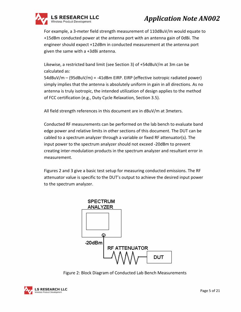
For example, a 3‐meter field strength measurement of 110dBuV/m would equate to
+15dBm conducted power at the antenna port with an antenna gain of 0dBi. The
engineer should expect +12dBm in conducted measurement at the antenna port
given the same with a +3dBi antenna.
Likewise, a restricted band limit (see Section 3) of +54dBuV/m at 3m can be
Figure 3: Recommended SA Settings for Sections 3.1, 3.2, 3.3 and 3.4
Spectrum analyzer settings that deviate from the above are noted in other sections.
The limits defined in Sections 3.1‐3.4 for a 15.247 device (>1GHz) refer to
conducted measurements using an average detector. From FCC section 15.35(b),
peak limits (utilizing a peak detector) are also limited to 20dB over the average
limit. Measurements utilizing both average and peak detectors are recommended in
initial bench analysis.
3 15.247 Applicable RF Limits
Section 3 outlines the various FCC limits and restrictions applicable to an 802.15.4
device filed under FCC part 15.247. Some of the limits are absolute (Sections 3.7‐
3.9) and some can be varied by applying a duty cycle relaxation factor (applicable to
Sections 3.1‐3.4 and defined in Section 3.5).
3.1 Upper Band Edge Limits and FCC Restricted Bands
The (16) 802.15.4 channels are not centered within the specified bandwidth.
Channel 11’s (Figure 1) center frequency or fundamental is 5 MHz from the lower
band edge. With a 5 MHz channel bandwidth (BW), the lower band edge is
therefore 2.5 MHz away from channel 11. Channel 26’s center frequency is 3.5 MHz
from the upper band edge. The upper band edge is 1.0MHz away from channel 26
given the specified 5 MHz channel BW.
Application Note AN002
Page 7 of 21
The FCC further limits RF energy allowed into defined restricted bands. The defined
2.4GHz band resides between two restricted bands with an average limit of 54
dBuV/m. The upper band edge is directly adjacent to a restricted band. These
restricted bands are given from 2 GHz to 24 GHz in Figure 4. Restricted bands
adjacent to the 2.4GHz ISM band are shown in bold text. Higher frequency
restricted bands are also an issue in amplified designs (see Section 3.4).
MHz GHz
2200‐2300 7.25‐7.75
2310‐2390 8.025‐8.5
2483.5‐2500 9.0‐9.2
2655‐2900 9.3‐9.5
3260‐3267 10.6‐12.7
3332‐3339 13.25‐13.4
3345.8‐3358 14.47‐14.5
3600‐4400 15.35‐16.2
4500‐5150 17.7‐21.4
5350‐5460 22.01‐23.12
23.6‐24.0
Figure 4: FCC Restricted Bands 2 GHz ‐ 24 GHz
Restricted bands are outlined in FCC part 15.205.
Figure 5 shows a modulated 802.15.4 signal at 250kbps. The center of the vertical
grid lines is the upper band edge. Note that the modulated envelope is wider on the
bottom; increasing the fundamental transmit power also increases RF energy
outside the channel BW into the restricted band.
Application Note AN002
Page 8 of 21
Figure 5: Upper Band Edge
The band edge limit is exceeded by 6dB in the Figure 5 example. Output power on
channel 26 is usually limited under 95dBuV/m or 0dBm for a constant transmission.
Amplified designs often cannot utilize this channel in utility despite its desired place
outside of Wi‐Fi. Practical design modifications such as additional filtering are
ineffective given the close proximity of the signal to the band edge. Any filter that
offered sufficient attenuation at the band edge would also reject part of the
intended signal.
Section 3.5 outlines relaxed limits due to duty cycle relaxation with periodic
transmissions that may be applicable to this section.
3.2 Lower Band Edge Limits
The upper band edge posed a limit on transmit power in the previous section; the
lower band edge will also limit transmit power on channel 11 to a lesser extent.
Recall that the specified channels are offset in the band.
1) The lower band edge is an additional 1.5MHz away from the channel 11
fundamental vs. the upper band edge to channel 26.
2) The adjacent restricted band is also 15MHz below the lower band edge.
Application Note AN002
Page 9 of 21
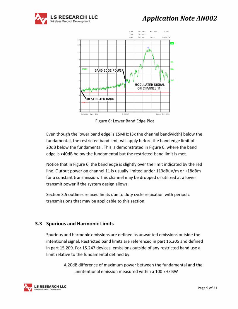
Figure 6: Lower Band Edge Plot
Even though the lower band edge is 15MHz (3x the channel bandwidth) below the
fundamental, the restricted band limit will apply before the band edge limit of
20dB below the fundamental. This is demonstrated in Figure 6, where the band
edge is >40dB below the fundamental but the restricted‐band limit is met.
Notice that in Figure 6, the band edge is slightly over the limit indicated by the red
line. Output power on channel 11 is usually limited under 113dBuV/m or +18dBm
for a constant transmission. This channel may be dropped or utilized at a lower
transmit power if the system design allows.
Section 3.5 outlines relaxed limits due to duty cycle relaxation with periodic
transmissions that may be applicable to this section.
3.3 Spurious and Harmonic Limits
Spurious and harmonic emissions are defined as unwanted emissions outside the
intentional signal. Restricted band limits are referenced in part 15.205 and defined
in part 15.209. For 15.247 devices, emissions outside of any restricted band use a
limit relative to the fundamental defined by:
A 20dB difference of maximum power between the fundamental and the
unintentional emission measured within a 100 kHz BW
Application Note AN002
Page 10 of 21
See FCC section 15.247(d) for definition on the limit stated above. Sections 3.1 and
3.4 define 15.247 limits within restricted bands.
One matter of concern is spurs offset from the fundamental by the reference
oscillator (e.g., 26MHz, 32MHz). These spurs may reside on adjacent restricted
bands and limit output power on channels other than 11 and 26. These spurs can
be noted in conducted measurement with a spectrum analyzer.
Spurious emissions not related to harmonics of the fundamental may not apply
the duty cycle correction factor outlined in Section 3.5. A good rule of thumb is to
place the DUT in receive mode on the same channel (frequency) if the spur
remains; a duty cycle correction factor may not be applied.
Figure 7: Example of Spurious Noise Offset from Unmodulated Carrier
Spurious emissions may also be outlined in the SoC manufacturer’s data sheet.
Application Note AN002
Page 11 of 21
3.4 Harmonic Emissions, Filtering and Shielding
Harmonics usually are caused by non‐linearity in the construction of the signal and
the PAs used to amplify. In the context of this document, the signal is amplified
internally to the chosen IC (often to 0dBm) and then again externally to reach the
system design goals.
Channel 11’s second harmonic has an average limit of 54dBuV/m, as it is in an FCC‐restricted band. The second and third harmonics of channel 18 (mid‐channel) and channel 25 also fall into restricted bands. Measurements are required to the 10th harmonic of each scanned channel (low, mid and high channel). In contrast to all previous sections, conducted and antenna radiated harmonic
emissions can be controlled by the engineer in hardware design by implementing
a low‐pass filter. Higher order harmonics likely can radiate off the PCB before this
additional filtering and antenna. The following design rules can help:
1) If a shield is implemented, place its boundaries over the entire circuitry,
including the final output filtering.
2) Ensure uninterrupted RF ground and supply decoupling.
3) Route all radio control traces into an inner PCB layer (e.g., PCB layer 3) not
interrupting the ground under the RF microstrip (e.g., PCB layer 2). Examples
of these RF control traces include the LNA and PA enable or bias and T/R
control. Connect back to the component layer with via close to the
component, with #4 below.
4) Place low ESR, in‐band bypass capacitors (e.g., 8pF) near the connection
point of all radio I/O control lines.
5) Ensure that all bypass capacitors have a good connection to ground by
utilizing at least three ground vias close to the component’s PCB ground pad.
Utilize the bottom layer and inner layer grounds with vias.
6) “Stitch” the PCB edge perimeter with vias tying together the PCB ground
planes, especially on small PCBs with RF traces close to the PCB edge.
7) With increased output power and amplifier characteristics, ensure that the
filtering provides adequate rejection up to the higher harmonics by
evaluating its response or the SRF of the discrete components.
Emissions radiated pre‐filter from the device are difficult to evaluate on the
bench. An FCC pre‐scan is recommended to evaluate all radiated emissions from
the device.
Application Note AN002
Page 12 of 21
3.5 Duty Cycle Relaxation
All previous sections assume a 100% duty cycle within stated FCC limits. The field
strength limits, in measurement, are a product of an average detector. For
periodic transmissions, a peak detector can be utilized with an associated
relaxation on the peak values. The calculated relaxation factor is applied to the
peak measurement to derive the average value. This correction can be applied to
both the fundamental and all associated harmonics.
This relaxation factor is calculated as:
RF [dB] = 20 log (TX ON [mS]/100mS)
Any relaxation is limited to 20dB. A 20dB relaxation factor equates to only a 10%
duty‐cycle or 10mS transmission within any 100mS window. ZigBee‐compliant
radios implement under a 50% duty cycle and thus an inherent ~6dB relaxation
factor. This can be applied to band edge limits of Section 3.1 and 3.2.
Applicable relaxation factor is defined in FCC 15.35(c).
This is important to note as the DUT is prepared for a trip to the compliance lab.
The test firmware should support the maximum duty cycle the product will see in
the field to evaluate benefit. Often the hardware is only exercised by a chip
manufacturer’s test tool and is not specific to the end application.
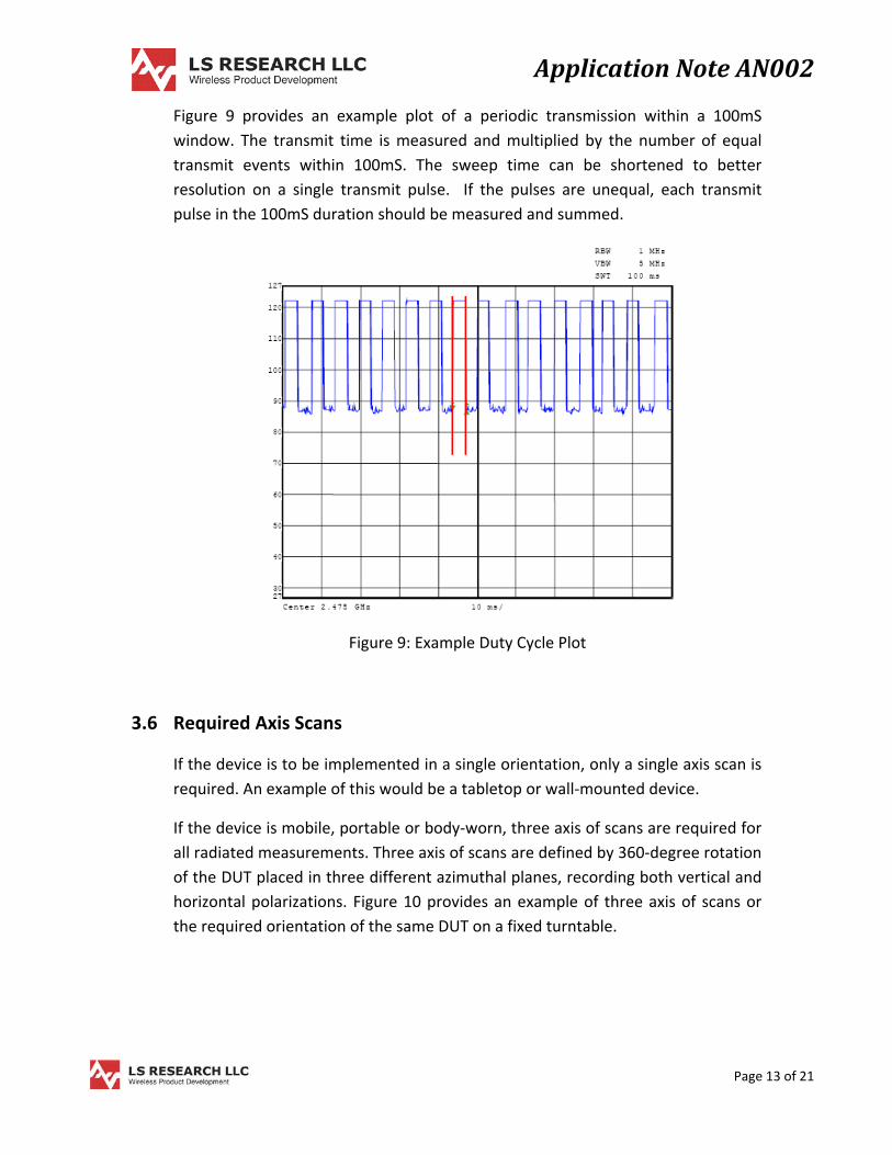
Figure 8 outlines recommended spectrum analyzer settings to determine the duty
cycle and inherent correction factor. The center frequency is set to the
fundamental frequency, and the frequency span is set to ZERO. The sweep time
determines the window of observation in the time domain, like an oscilloscope.
Figure 11: Recommended SA Settings for PSD Measurement
PSD was measured on an 802.15.4‐compliant radio with an output power of
0dBm. Figure 11 utilizing an 802.15.4 design exhibits a peak PSD of ‐14dBm in any
3kHz BW from a conducted output power of 0dBm. Since the modulation
envelope should be fixed, a 1:1 correlation from increased power output should
be expected. Therefore, a 802.15.4 design is expected to be limited to a
conducted output power of +22dBm due to the PSD limit.
Application Note AN002
Page 15 of 21
Figure 12: PSD Measurement Example
‐14dBm (measured) + 8dBm (limit) = 22dBm
0dBm (per Figure 11) + 22dBm = 22dBm conducted power output to PSD limit
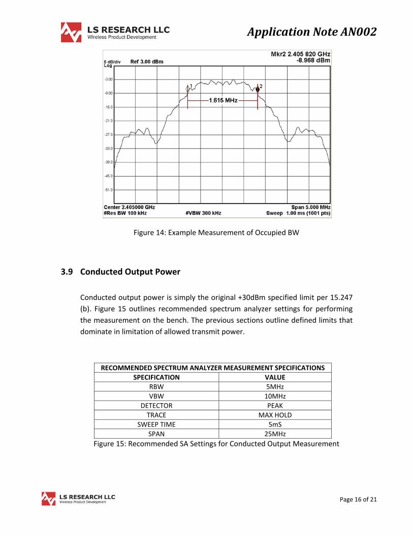
3.8 Occupied Bandwidth
Since the modulation and data rate are fixed in the transceiver, the occupied bandwidth (BW) is defined as the modulation type and data rate inherent to the core SoC radio. FCC section 15.247 (a) (2) states that the minimum 6dB bandwidth shall be at least 500kHz. With a properly operating 802.15.4 radio, this FCC limit should pose no compliance issues.
Figure 15: Recommended SA Settings for Conducted Output Measurement
Application Note AN002
Page 17 of 21
4 15.247 Conducted Limit Summary
Figure 16 summarizes Section 3 to assist the engineer in bench evaluation.
Test 15.247 Restricted Band Limit
Calculated Conducted Restricted Band Limit
15.247 Non‐Restricted Band Limit
Duty‐Cycle Relaxation Allowed?
Upper Band Edge (2.480 GHz)
54dBuV/m average
detector @ 2.4835 GHz
‐41dBm Ave ‐21dBm Peak @ 2.4835
GHz
N/A; upper band edge is near
restricted band
Defined as 20dB below fundamental
@ 2.480 GHz
Yes
Lower Band Edge (2.405 GHz)
54dBuV/m average
detector @ 2.390 GHz
‐41dBm Ave ‐21dBm Peak @ 2.390 GHz
N/A; upper band edge is near
restricted band
Defined as 20dB below fundamental
@ 2.405 GHz
Yes
Spurious* 54dBuV/m average detector
‐41dBm Ave ‐21dBm Peak
20dB below fundamental
No*
Harmonics to 24.8GHz
54dBuV/m average detector
‐41dBm Ave ‐21dBm Peak
20dB below fundamental
Yes
PSD N/A, in band 8dBm in 3kHz BW No
Occupied BW
N/A, in band Minimum of 500kHz in 6dB BW
N/A
Output power
N/A, in band 1W/ 30dBm No
*Spurious emissions not related to the fundamental (i.e., local oscillator
reference spurs). Figure 16: Limits Applicable to 802.15.4 Devices Filed Under FCC 15.247
Application Note AN002
Page 18 of 21
5 Compliance Pre‐Scan
A pre‐scan at the compliance lab can determine issues with harmonics, spurious
emissions, other unintentional radiation, line‐conducted issues or the operation of
the test modes. This initial feedback can help the design engineer evaluate
necessary changes. The optimal time for a pre‐scan is when the hardware is
mature with minimum PCB rework (jumper wires and cut traces) and before the
final “pilot” revision. This allows all potential issues to be addressed before the
final revision and scheduling a full scan. Most design cycles are scheduled within a
fixed number of revisions to product release. A pre‐scan will often reduce internal
costs by addressing previously unknown issues before the final scheduled revision.
Before a device is submitted, the following information should be prepared to
allow the lab to determine required tests and correctly manipulate the submitted
DUT.
1) Provide a short description of the technology: what it is, how it will be used,
and its purpose.
2) Specify how the device is powered: battery and type, AC, DC, wall transformer,
supplied voltage, and so on.
3) Is the device fixed, mobile, or integrated into another system?
4) What channels are utilized? 5) What is the maximum power output? Is the power output variable per
channel? Is the power output fixed but varying across channels? Specify the operation per each channel.
6) What antennas are used and supplied, and what is the specified antenna gain? 7) The unit should be able to exhibit a constant transmit mode to ensure that all
emissions are captured during DUT rotation. 8) The unit should be able to exhibit a pulsed transmit mode representative of
production utility to allow evaluation of the maximum duty cycle of the device and any inherent relaxation to the compliance limits.
9) Is there any cabled communication to the device?
10) Is there a pre‐existing FCC filing for the device?
11) Is the device intended for filing as a module?
12) Will the device be offered in differing variants? Specify any changes to the
device, even those that are non‐RF.
13) How does the EMC engineer exercise the operating and test modes? What
mode(s) are required for each channel?
Application Note AN002
Page 19 of 21
6 Conclusions
An amplified 802.15.4 radio requires some background on FCC certification that can
affect initial system design, PCB design, data through‐put, amplifier choice,
shielding, channel allocation and required output filtering.
Investing in an abbreviated compliance pre‐scan with mature hardware before
conducting a ”final” design revision without knowledge of potential FCC issues will
bring the product to the production level, saving cost and time.
Application Note AN002
Page 20 of 21
7 Abbreviations and Definitions
SoC “System on a Chip,” defined as a combined radio transceiver and microcontroller
PA Power amplifier for increasing transmit power
DSSS Direct Sequence Spread Spectrum
dBi dB relative to a theoretical isotropic antenna. A 0dBi antenna has no gain or loss.
Front‐End The RF components between the SoC and the antenna
LNA Low noise amplifier for increasing receive gain and sensitivity
Balun A transformer device for impedance matching a differential signal path to single‐ended
T/R switch An RF switch for directing the signal along the transmit or receive paths
Spurs Unwanted emissions outside the intentional signal, excluding harmonics
Harmonics Inter‐modulation products due to non‐linearity of devices
EIRP Effective isotropic radiated power: A field‐strength‐derived value for conducted power assuming an isotropic antenna
SRF Self resonant frequency: the frequency at which parasitic reactance exceeds the intentional
Isotropic Uniform response in all directions
LPF Low pass filter: attenuates frequencies above the pass‐band
BW Bandwidth: the product within a defined span of frequency
PSD Power spectral density: power within a defined bandwidth
RBW Resolution bandwidth: determines the limit in frequency BW that can be resolved
VBW Video bandwidth: determines the limit in frequency BW that can be displayed