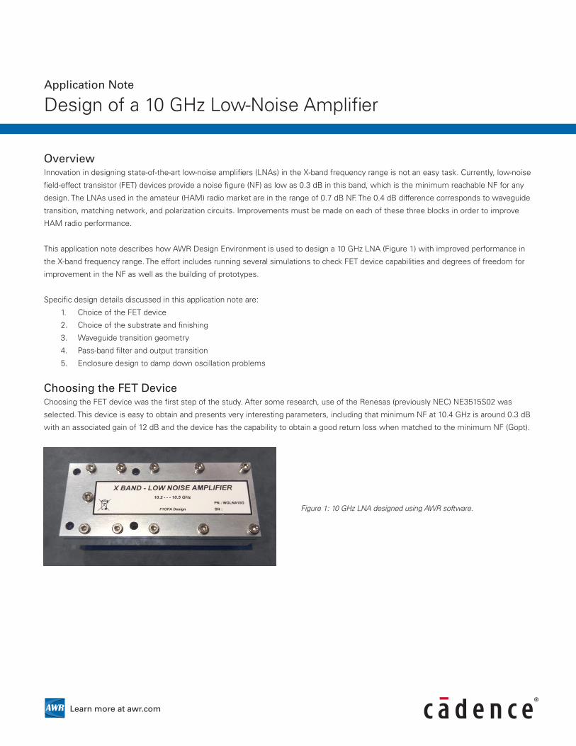
AWR Learn more at awr.com Overview Innovation in designing state-of-the-art low-noise amplifiers (LNAs) in the X-band frequency range is not an easy task. Currently, low-noise field-effect transistor (FET) devices provide a noise figure (NF) as low as 0.3 dB in this band, which is the minimum reachable NF for any design. The LNAs used in the amateur (HAM) radio market are in the range of 0.7 dB NF. The 0.4 dB difference corresponds to waveguide transition, matching network, and polarization circuits. Improvements must be made on each of these three blocks in order to improve HAM radio performance. This application note describes how AWR Design Environment is used to design a 10 GHz LNA (Figure 1) with improved performance in the X-band frequency range. The effort includes running several simulations to check FET device capabilities and degrees of freedom for improvement in the NF as well as the building of prototypes. Specific design details discussed in this application note are: 1. Choice of the FET device 2. Choice of the substrate and finishing 3. Waveguide transition geometry 4. Pass-band filter and output transition 5. Enclosure design to damp down oscillation problems Choosing the FET Device Choosing the FET device was the first step of the study. After some research, use of the Renesas (previously NEC) NE3515S02 was selected. This device is easy to obtain and presents very interesting parameters, including that minimum NF at 10.4 GHz is around 0.3 dB with an associated gain of 12 dB and the device has the capability to obtain a good return loss when matched to the minimum NF (Gopt). Application Note Design of a 10 GHz Low-Noise Amplifier Figure 1: 10 GHz LNA designed using AWR software.
Transcript
AWR Learn more at awr.com
Overview Innovation in designing state-of-the-art low-noise amplifiers (LNAs) in the X-band frequency range is not an easy task. Currently, low-noise
field-effect transistor (FET) devices provide a noise figure (NF) as low as 0.3 dB in this band, which is the minimum reachable NF for any
design. The LNAs used in the amateur (HAM) radio market are in the range of 0.7 dB NF. The 0.4 dB difference corresponds to waveguide
transition, matching network, and polarization circuits. Improvements must be made on each of these three blocks in order to improve
HAM radio performance.
This application note describes how AWR Design Environment is used to design a 10 GHz LNA (Figure 1) with improved performance in
the X-band frequency range. The effort includes running several simulations to check FET device capabilities and degrees of freedom for
improvement in the NF as well as the building of prototypes.
Specific design details discussed in this application note are:
1. Choice of the FET device
2. Choice of the substrate and finishing
3. Waveguide transition geometry
4. Pass-band filter and output transition
5. Enclosure design to damp down oscillation problems
Choosing the FET Device Choosing the FET device was the first step of the study. After some research, use of the Renesas (previously NEC) NE3515S02 was
selected. This device is easy to obtain and presents very interesting parameters, including that minimum NF at 10.4 GHz is around 0.3 dB
with an associated gain of 12 dB and the device has the capability to obtain a good return loss when matched to the minimum NF (Gopt).
Application Note
Design of a 10 GHz Low-Noise Amplifier
Figure 1: 10 GHz LNA designed using AWR software.
The NF and RL circles were calculated in Microwave Office software with an excellent tool for evaluating the matching capability. As
shown in the Figure 2, the NE3515S02 is optimized to be used for X-band low-noise applications. The cross area between RL (blue) and
NF (red) circles show an expected NF ~0.4 dB and RL ~10 dB
Choice of Substrate and Finishing Substrate and finishing are sources of loss and must be selected with care. Typically, there is a compromise between copper loss,
dielectric loss, and radiation loss for several reasons. Wide copper lines above dielectric substrate have bigger dielectric loss than thinner
lines. On the other hand, small copper geometries experience higher copper loss. Any discontinuity on the transmission line shows
radiation loss.
Taking into account the information in the datasheet of the device and the different transmission line impedances used on the printed
circuit board (PCB), the best compromise was to use the RO4003C with a thickness about 0.305 mm. This economical, low-loss ceramic
laminate is widely recommended by many manufacturers and fits the requirements of this design perfectly.
Low-Loss / Wideband Waveguide Transition The critical part of the LNA is the input stage. The input stage should transform the input impedance of the LNA (usually 50 Ohms) to the
Gopt, as discussed before. It is important to be careful to minimize the losses by having a bandwidth as broad as possible. In an optimum
LNA design, the use of a waveguide-to-microstrip adapter is recommended to minimize the size, as well as the loss.
A common approach (DB6NT [1], HB9BBD [2]) is to design the LNA and waveguide (WG) adapter separately with a standard real
impedance of 50 Ohms. However, this option has several disadvantages, including narrow-band matching response, sensitivity of the
process (mechanical and PCB), and matching network losses.
Why not use Gopt as a reference impedance for the WG transition? This strategy needed a brand-new WG adapter design optimized to
show, at the microstrip reference plane, the Gopt. The disadvantages were less present, but the problem was the fact that the
impedance was complex (real + imaginary) and special care had to be taken during simulation of the design to avoid impedance phase
plan rotation, which would completely scrap the Gopt point.
Figure 2: NF and associated input RL calculated in Microwave Office.
Figure 3 shows the optimized WG adapter geometry. The use of an impedance transformer with stepping height allowed for reduction of
the waveguide impedance viewed from the microstrip probe. This lower impedance, combined with an optimum shape of the probe and
back sort position, provided a broader bandwidth.
The simulation of the input was realized using Analyst™ 3D FEM EM simulator. The first port was placed at the waveguide and the second
port was placed at the reference plane of the device. After some adjustments (impedance transformer, probe, and back sort), the result
(Figure 4) was very interesting and confirmed the potential for this type of design by matching to Gopt from 9 GHz to 12 GHz with a
variation of only 0.1 dB from the NF min.
Figure 3: Optimized WG adapter geometry.
Figure 4: Analyst simulation results of the input WG to the microstrip.
Planar Structure Analysis After the input transition, the next step was to design all the planar structures (Figure 5). Here it was decided to use two amplification
stages (gain >20 dB) and a band-bass filter at the output to reduce the gain out of band.
A first optimization to preserve the broadband performance was done with Microwave Office software and then the final adjustment was
performed with AXIEM 3D planar EM simulator, which allowed for the different coupling occurring between the printed elements and
mechanical parts (covers, walls, and more) to be taken into account.
Regarding the band-pass filter (Figure 6), the choice of the bandwidth was defined by taking into account the different parameters
impacted by the material and the process (permittivity, etching, and more).
Figure 5: Design of the planar structures.
Figure 6: Band-pass filter with choice of bandwidth defined by the different parameters impacted by the material and process.
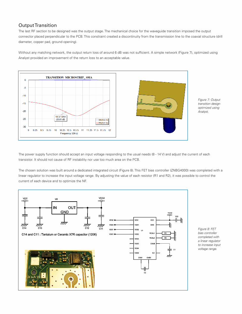
Output Transition The last RF section to be designed was the output stage. The mechanical choice for the waveguide transition imposed the output
connector placed perpendicular to the PCB. This constraint created a discontinuity from the transmission line to the coaxial structure (drill
diameter, copper pad, ground opening).
Without any matching network, the output return loss of around 6 dB was not sufficient. A simple network (Figure 7), optimized using
Analyst provided an improvement of the return loss to an acceptable value.
The power supply function should accept an input voltage responding to the usual needs (8 - 14 V) and adjust the current of each
transistor. It should not cause of RF instability nor use too much area on the PCB.
The chosen solution was built around a dedicated integrated circuit (Figure 8). This FET bias controller (ZNBG4000) was completed with a
linear regulator to increase the input voltage range. By adjusting the value of each resistor (R1 and R2), it was possible to control the
current of each device and to optimize the NF.
Figure 7: Output transition design optimized using Analyst.
Figure 8: FET bias controller completed with a linear regulator to increase input voltage range.
Enclosure Design It is important not to consider the enclosure as a simple box. In the X-frequency band, the effect of the cover becomes a problem.
Generally, an absorber is placed inside the enclosure to suppress the oscillations. The problem is the absorber’s reliability over time due
to factors such as temperature and humidity. For this design, it was decided to suppress all the oscillation problems by designing a
specific cover, which prevented any emergence of propagation-guided modes such as partitioning, height, and area. Figure 9 shows the
enclosure details of the cover.
The waveguide input was put in the second part of the enclosure with the impedance transformer and the output coaxial connector and
the PCB was placed between these two parts. With this type of design, the positioning of all the parts was simple and it was not
necessary to glue the PCB. The machining of the parts was performed on a computer numeric control (CNC) machine to ensure
mechanical precision and good reproducibility over the batch.
After testing different finishings, the decision was made to select SERTEC 650. This finishing is compatible with the European Union
Registration, Evaluation, Authorization, and Restriction of Chemicals (REACH) requirement for human health and environmental risks, and
the effect on the performance is not measurable. The main advantage is protection against oxidation, which ensures the device will
function for a long period of time.
Figure 9: Enclosure detail of cover designed to suppress all oscillation problems.
Simulation Results All the different simulation blocks performed with Analyst and AXIEM EM simulators were imported into Microwave Office software to
obtain the complete response of the amplifier. With this methodology, it was very fast and easy to optimize each subcircuit independently
to the desired response. The final result of the simulation (Figure 10) was encouraging and the broadband specification, over the
bandwidth of the filter, was maintained. It should be noted that the loss of the input waveguide and the roughness of the printed lines
was not taken into account in the calculation.
Measurement Results Ten prototypes were assembled and measured to see the dispersion. No specific tuning was necessary on the PCB or enclosures. By
looking at the typical measurement (Figure 11), it was found that the results were very close to the simulation. The NF was 0.1 to 0.15 dB
higher than expected, but still very good (under 0.6db) over 700 MHz of bandwidth. As predicted by simulation, the input return loss
validated the concept of the waveguide to microstrip transition, and the stability was guaranteed by the mechanical design.
Figure 11: Measurement results showing that measurements were very close to simulation.
Figure 10: Simulation results of final simulation done in Microwave Office.