Application of a novel microwave plasma treatment for the sintering of nickel oxidecoatings for use in dye-sensitized solar cells
Muhammad Awais a, Mahfujur Rahman a, J.M. Don MacElroy b, Danilo Dini c,Johannes G. Vos c, Denis P. Dowling a,b,⁎a School of Electrical, Electronic and Mechanical Engineering, University College Dublin, Irelandb School of Chemical and Bioprocess Engineering, University College Dublin, Irelandc School of Chemical Sciences, Dublin City University, Ireland
Keywords:Dye-sensitized solar cellsNickel oxideNanoparticlesMicrowave plasma sinteringDye sensitization
In this study the use of microwave plasma sintering of nickel oxide (NiOx) particles for use as p-typephotoelectrode coatings in dye-sensitized solar cells (DSSCs) is investigated. NiOx was chosen as thephotocathode for this application due to its stability, wide band gap and p-type nature. For high lightconversion efficiency DSSCs require a mesoporous structure exhibiting a high surface area. This can beachieved by sintering particles of NiOx onto a conductive substrate. In this study the use of both 2.45 GHzmicrowave plasma and conventional furnace sintering were compared for the sintering of the NiOx particles.Coatings 1 to 2.5 μm thick were obtained from the sintered particles (mean particle size of 50 nm) on 3 mmthick fluorine-doped tin oxide (FTO) coated glass substrates. Both the furnace and microwave plasmasintering treatments were carried out at ~450 °C over a 5 min period. Dye sensitization was carried out usingErythrosin B and the UV–vis absorption spectra of the NiOx coatings were compared. A 44% increase in thelevel of dye adsorption was obtained for the microwave plasma sintered samples as compared to thatobtained through furnace treatments. While the photovoltaic performance of the DSSC fabricated using themicrowave plasma treated NiOx coatings exhibited a tenfold increase in the conversion efficiency incomparison to the furnace treated samples. This enhanced performance was associated with the difference inthe mesoporous structure of the sintered NiOx coatings.
and Materials Science Centre,.: +353 1 716 1747; fax: +353
Dye-sensitized solar cells (DSSCs) show considerable potential as arelatively low cost alternative to silicon based solar cells. These cellswere developed by Grätzel and co-workers in 1991 [1] and there iscurrently a considerable focus on enhancing their light conversionefficiency and stability [2–8]. In the case of conventional DSSCs, dyesensitization involves solely the semiconductor anode made of n-typeTiO2 nanoparticles [1–8]. The counter electrode is generally a metalliccathode with no photoelectrochemical activity [1–8]. To date thehighest conversion efficiency obtained of 11% [9], is less than the bestsilicon based thin-film cells [10]. A method of further enhancing thelight conversion efficiency as suggested by He et al. is to substitute thecathode with a dye-sensitized photoactive p-type metal oxide. Thistandem dye-sensitized solar cell design utilizes more of the solarspectrum [11]. The efficiency, however of p-type metal oxides is stillvery low, which limits their effectiveness in tandem DSSCs [12].
Amongst the potential reasons highlighted for the poor conversionefficiency of the cathodewithin tandemDSSC, themore critical are theinefficient light absorption capability, poor charge injection efficiencyand charge transport rate, along with inner resistance [13,14]. Onemethod of improving this efficiency would be the preparation ofp-type metal electrodes with a surface exhibiting high porosity with-out sacrificing the mechanical stability of the resulting coatings. Thissurface morphology ensures higher light absorption by the monolayerof adsorbed dye, while keeping an intimate contact between the p-typematerial and thedyemolecules. This in turn reduces the inner resistanceand hence improving the charge injection efficiency.
The focus of this research is on nickel oxide (NiOx) coatings, whichhas a considerable potential for use as a cathode in tandem cells [11].This is due to their p-type nature [15], excellent chemical stability, inaddition towell defined optical and electrical properties [16].Moreover,NiOx is considered as a model semiconductor substrate due to its wideband-gap energy range from 3.6 to 4.0 eV depending on the amount ofNi(III) sites [15]. NiOx films have been fabricated by various techniqueswhich include spin coating, dipping, electrochemical deposition [17],magnetron sputtering [18–20] and sol–gel [21–25]. With the exceptionof electrochemical techniques, the other deposition methods requiresubsequent thermal treatments in order to enhance the density of the
Fig. 1. (a) XRD spectra of 1 to 10 min rapid discharge sintered NiOx coatings (1–2 μm).The crystallite size information was calculated using the Scherrer equation. (b) UV–visabsorbance spectroscopy of 1–2 μm thick dye sensitized NiOx coatings (sintered 1 to10 min).
S246 M. Awais et al. / Surface & Coatings Technology 205 (2011) S245–S249
coatings [21–26], to obtain crystalline structure in the as depositedsputtered coatings [26] and to remove the binder in the case of sol–geldeposited coatings [21–25]. Typically sintering conditions of 300–450 °C for 30 to 60 min are reported [21–25].
There have also been a large number of reports in the literature onthe interaction between microwave radiation and materials [27,28].The ability of microwaves to penetrate the surface of the work pieceenables rapid volumetric heating in microwave processing, reducingthe need for external heat sources [27]. Advantages of non-plasmamicrowave processing over furnace treatment are reported to includefiner grain sizes, rounded porosity and higher ductility and toughness[29]. Increased shrinkage rates and decreased grain sizes can beachieved with microwave plasma treatments compared with furnacesintering [30–32]. With these advantages and significantly reducedcycle times, microwave-assisted plasma sintering offers an economicroute for the production and reduced energy consumption per process.In this study, the use of microwave plasma as a sintering technology forthe NiOx particles is investigated for the first time. The microwaveplasma treatment technique is called Rapid Discharge Sintering (RDS)and it involves the immersion of the samples in microwave plasmaformedunder reducedpressure conditions. In this study a comparison ismade between the RDS sintered NiOx coatings and those obtained usingconventional furnace sintering. In addition to a comparison of theirphysical properties, the performance of the sintered coatings in dye-sensitized solar cells was also evaluated.
The objective of this study is to prepare p-type NiOx coatings to beused as a photocathode in tandemDSSCs application. The challenge is todevelop coatings exhibiting mesoporous properties with enhancedinterconnectivity between particles and the FTO/NiOx interface to reducethe inner resistance. The mesoporous structure of the p-type electrodealso favors dye adsorption and charge injection from the sensitizer tothe photocathode with resulting increase of the light-to-photocurrentconversion efficiency. In this study in addition to comparing the influenceof sintering process technology on the performance of the NiOx coatings,a second object is to evaluate how the duration of RDS sintering treat-ment influences coating performance.
2. Experimental
2.1. Sample preparation and deposition of NiOx coatings
The NiOx particulate layer was deposited onto fluorine doped tinoxide (FTO) glass (3 mm thick) supplied by Mansolar. The glasssubstrates (2×2 cm) were ultrasonically cleaned in propanol followedby acetone, each for 5 min prior to the application of the NiOx particulatelayer. The NiOx nanoparticles (~50 nm) were suspended in methanol(20 mg/ml) and the particulate layer NiOx is deposited by spraying usinga similar technique to that described previously [33]. The microwave-assistedplasma sinteringprocess knownas rapiddischarge sinteringwascarried out using a circumferential antenna plasma (CAP) microwavesystem described in detail elsewhere [34]. The plasma was formed at apressure of 5 mbar in an argon and oxygen (10:1) atmosphere. Inputpowers of 2.4 kWwere supplied fromaMuggemicrowave power supplyoperating at a frequency of 2.45 GHz. The initial study with microwaveplasma sintering evaluated the influence of sintering time over a 1 to10 min period. Substrate temperatures were measured using a LASCONQP003 two-colour pyrometer from Dr Merganthaler GmbH & Co. Thefurnace treatmentswere carried out in air using a Carbolite Furnace (RHF1200). For both the furnace and microwave plasma sintering systemsthree NiOx samples were treated simultaneously at temperatures of~450 °C, for a treatment time of 5 min.
2.2. Characterization equipment
The NiOx film thickness was measured by step height measure-ment using a WYKO NT1100 optical profilometer in vertical scanning
interferometry (VSI) mode. For the cross sectional investigations, thecoatings were mounted on stubs using double-sided carbon tape, andsputter coatedwith platinum, using an Emitech K575X sputter coatingunit, to prevent surface charging by the electron beam. Samples werethen examined using a FEI Quanta 3D FEG DaulBeam (FEI Ltd,Hillsboro, USA). X-ray diffraction (XRD) measurements were carriedout using a Siemens D500 diffractometer operating at 40 kV and30 mA with Cu Kα radiation in normal diffraction mode at 0.2°/minscan rate in the 2θ range of 40–50°.
2.3. Dye sensitization, UV–vis measurements and IV-characteristics
NiOx coatings were sensitized with 0.3 mM Erythrosin B (ERY) dye[11,17,22], in a 99.8% ethanol solution for 24 h. The dye adsorptionwas investigated in transmission mode using an AnalytikJena Specord210 UV–vis spectrophotometer in the wavelength range of 350–700 nm. The photovoltaic performance (I-V characteristic) of dyesensitized NiOx coatings were analyzed in two electrode configurationusing 870 Wm−2 AM 1.5 solar simulator and platinum coated FTOwas used as a counter electrode. The p-type behavior of ERY-sensitized NiOx coatings was observed using a custom madephotoelectrochemical cell in three-electrode configuration: workingelectrode was ERY-NiOx on FTO; counter electrode was platinum, anda standard calomel electrode (SCE) was utilized as the referenceelectrode. The electrolyte was 0.5 M LiI and 0.05 M I2 in propylenecarbonate (from Sigma-Aldrich).
Loosely adherent NiOx particulate layers were prepared from themetal oxide/methanol slurry using the spray technique. The layerthickness was maintained between 1 and 2 μm. The initial study withthe RDS technique evaluated the influence of sintering time over a 1 to10 min period, on coating performance. Using the Scherrer equa-tion [35] to examine the XRD data, an increase in crystallite size from6.5 to 19.0 nmwas observed on increasing the sintering time from 1 to10 min (Fig. 1a). Only a small decrease in the NiOx particulate layers'coating thickness was observed after sintering.
In order to sensitize p-type NiOx coatings, the oxide was treatedwith ERY dye. The UV–vis absorption spectra of the samples preparedunder different sintering times showed a gradual decrease (Fig. 1b) ofthe amount of adsorbed dye for the coatings with the smallercrystallite size to thosewith the largest crystallites. In order to preparep-type DSSCs, the ERY sensitized NiOx electrodes were squeezedtogether with platinum coated FTO using binder clips. The electrolytewas filled uniformly into the interelectrode space by capillary forces.To optimize the NiOx coatings preparation, the open current photo-voltage (VOC), the short circuit photocurrent density (JSC) and overallphotocurrent efficiency (η), were measured as a function of sinteringtime. Fig. 2a details the I-V characteristics of the ERY sensitized NiOx
coatings sintered at different times (thickness: 1–2 μm). Though dyeadsorption levels were higher for the 1 min sintered coatings, the5 min sintered sample (RDS5) exhibited the highest efficiency. These
0 15 30 45 60 75 90 1050.0
0.1
0.2
0.3
0.4
0.5
0.6
V / mV
RDS_1min RDS_3min RDS_5min RDS_7min RDS_10min
-1000 -800 -600 -400 -200 0 200
-600
-400
-200
0
200
J / µ
m c
m-2
Darkcurrent Photocurrent
FTO
I: 870 Wm -2 AM1.5 solar simulator
Electrolyte: 0.5 M LiI and 0.05 M I2 in
Propylene Carbonate
RDS
3min 53.74 0.44 26 0.0067
5min 72.14 0.53 28 0.0118
7min 73.04 0.50 29 0.0116
10min 95.00 0.33 31 0.0106
RDS
3min 53.74 0.44 26 0.0067
5min 72.14 0.53 28 0.0118
7min 73.04 0.50 29 0.0116
10min 95.00 0.33 31 0.0106
J / m
Acm
-2
RDS_1min RDS_3min RDS_5min RDS_7min RDS_10min
Applied potenial / mV vs SCE
Darkcurrent Photocurrent
Working electrode: ERY-sensitized NiO x on
Counter electrode: Platinum
(a)
(b)
RDS 1min
3min 53.74 0.44 26 0.0067
5min 72.14 0.53 28 0.0118
7min 73.04 0.50 29 0.0116
10min 95.00 0.33 31 0.0106
VOC (mV)
ISC (mAcm2)
FF Efficiency(%)
RDS 59.28 0.32 29 0.0062
3min 53.74 0.44 26 0.0067
5min 72.14 0.53 28 0.0118
7min 73.04 0.50 29 0.0116
10min 95.00 0.33 31 0.0106
Fig. 2. (a) Photovoltaic performance of ERY sensitized NiOx coatings (1–2 μm thick)using the light from AM 1.5 solar simulator (I: 870 Wm−2). Electrolyte: 0.5 M LiI and0.05 M I2 in propylene carbonate. (b) Current density vs applied potential curves for5 min, 2.5 μm thick RDS sintered NiOx coatings sensitized with ERY.
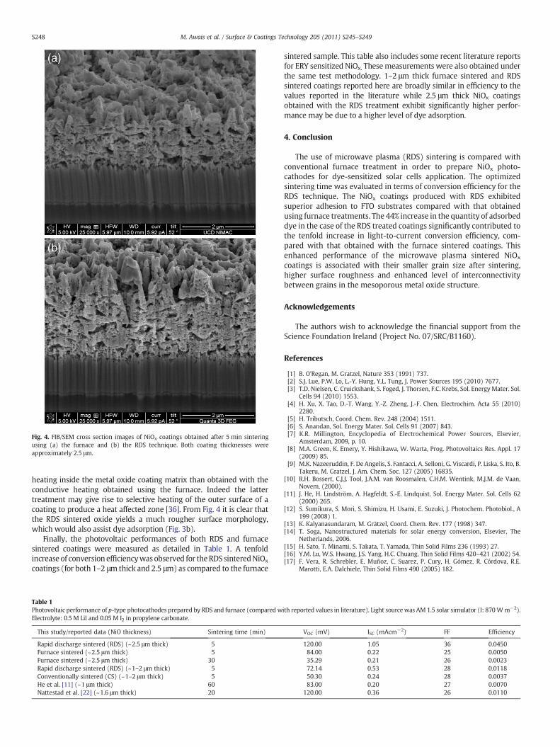
sintering conditions facilitate a high level of dye diffusion, whilemaintaining interconnectivity between individual oxide grainsand FTO/NiOx interface. Thus the mesoporous sintered metal oxidestructure facilitates efficient charge injection from the ERY dye. Asubsequent studywith 2.5 μm thick NiOx coatings also demonstrated asimilar trend. The p-type behavior of ERY-sensitized NiOx coatings(RDS5) was investigated as shown in Fig. 2b, the curves in darkand under UV illumination demonstrated cathodic photocurrentsof ERY-sensitized NiOx coatings with an onset of photocurrent atapproximately +120 mV vs (standard calomel electrode) the SCEreference [11]. In order to compare the performance of RDS tech-nique with conventional furnace treatments, the NiOx coatings werealso sintered at 450 °C for 5 min in a box furnace. The properties ofthe furnace sintered coatings were then compared with thoseobtained using the RDS technique. XRD examination of the sinteredNiOx coatings demonstrated a significantly smaller crystallite size of6.5 nm for the microwave plasma sintered samples, as compared tothe 14 nm obtained after the furnace treatment (Fig. 3a). Thus thesmaller grain size along with more homogeneous heating/sintering isachieved using the RDS technique thus helping to maintain themesoporous structure of the NiOx nanoparticles. A cross section of thecoatings obtainedby FIB/SEM from the two sintering techniques is givenin Fig. 4. It is clear from these images that the RDS sintered coatingexhibits a higher level of bonding at the interface between the NiOx
coating and the FTO layer. A possible explanation for this is that the RDStreatment involves volumetric heating, which provides more effective
350 420 490 560 630 7000.0
0.5
1.0
1.5
2.0
2.5
Abs
orba
nce
/ a.u
.
Wavelength / nm
ERY-sensitized NiOx sintered with RDS ERY-sensitized NiOx sintered with furnace Erythrosin B dye in solution
(a)
(b)
40 41 42 43 44 45 46 47 480
200
400
600 Crystallite size (nm)
measured using Scherrer formula
RDS 5 CS 5
6.5 14
(NiO (200))
Inte
nsity
/ a.
u.
2-theta / degree
NiO treated with CS NiO treated with RDS
Fig. 3. (a) XRD spectra of 2.5 μm thick NiOx coatings sintered for 5 min using furnaceand the RDS technique. The crystallite size was calculated using the Scherrer equation.(b) UV–vis absorbance spectra of 2.5 μm thick ERY sensitized-NiOx coatings sintered for5 min using the furnace and the RDS technique.
Fig. 4. FIB/SEM cross section images of NiOx coatings obtained after 5 min sinteringusing (a) the furnace and (b) the RDS technique. Both coating thicknesses wereapproximately 2.5 μm.
S248 M. Awais et al. / Surface & Coatings Technology 205 (2011) S245–S249
heating inside the metal oxide coating matrix than obtained with theconductive heating obtained using the furnace. Indeed the lattertreatment may give rise to selective heating of the outer surface of acoating to produce a heat affected zone [36]. From Fig. 4 it is clear thatthe RDS sintered oxide yields a much rougher surface morphology,which would also assist dye adsorption (Fig. 3b).
Finally, the photovoltaic performances of both RDS and furnacesintered coatings were measured as detailed in Table 1. A tenfoldincrease of conversion efficiencywasobserved for the RDS sinteredNiOx
coatings (for both 1–2 μm thick and 2.5 μm) as compared to the furnace
Table 1Photovoltaic performance of p-type photocathodes prepared by RDS and furnace (compared wElectrolyte: 0.5 M LiI and 0.05 M I2 in propylene carbonate.
This study/reported data (NiO thickness) Sintering time (min)
sintered sample. This table also includes some recent literature reportsfor ERY sensitized NiOx. Thesemeasurements were also obtained underthe same test methodology. 1–2 μm thick furnace sintered and RDSsintered coatings reported here are broadly similar in efficiency to thevalues reported in the literature while 2.5 μm thick NiOx coatingsobtained with the RDS treatment exhibit significantly higher perfor-mance may be due to a higher level of dye adsorption.
4. Conclusion
The use of microwave plasma (RDS) sintering is compared withconventional furnace treatment in order to prepare NiOx photo-cathodes for dye-sensitized solar cells application. The optimizedsintering time was evaluated in terms of conversion efficiency for theRDS technique. The NiOx coatings produced with RDS exhibitedsuperior adhesion to FTO substrates compared with that obtainedusing furnace treatments. The 44% increase in the quantity of adsorbeddye in the case of the RDS treated coatings significantly contributed tothe tenfold increase in light-to-current conversion efficiency, com-pared with that obtained with the furnace sintered coatings. Thisenhanced performance of the microwave plasma sintered NiOx
coatings is associated with their smaller grain size after sintering,higher surface roughness and enhanced level of interconnectivitybetween grains in the mesoporous metal oxide structure.
Acknowledgements
The authors wish to acknowledge the financial support from theScience Foundation Ireland (Project No. 07/SRC/B1160).
References
[1] B. O'Regan, M. Gratzel, Nature 353 (1991) 737.[2] S.J. Lue, P.W. Lo, L.-Y. Hung, Y.L. Tung, J. Power Sources 195 (2010) 7677.[3] T.D. Nielsen, C. Cruickshank, S. Foged, J. Thorsen, F.C. Krebs, Sol. Energy Mater. Sol.
2280.[5] H. Tributsch, Coord. Chem. Rev. 248 (2004) 1511.[6] S. Anandan, Sol. Energy Mater. Sol. Cells 91 (2007) 843.[7] K.R. Millington, Encyclopedia of Electrochemical Power Sources, Elsevier,
Amsterdam, 2009, p. 10.[8] M.A. Green, K. Emery, Y. Hishikawa, W. Warta, Prog. Photovoltaics Res. Appl. 17
(2009) 85.[9] M.K. Nazeeruddin, F. De Angelis, S. Fantacci, A. Selloni, G. Viscardi, P. Liska, S. Ito, B.
Takeru, M. Gratzel, J. Am. Chem. Soc. 127 (2005) 16835.[10] R.H. Bossert, C.J.J. Tool, J.A.M. van Roosmalen, C.H.M. Wentink, M.J.M. de Vaan,
Novem, (2000).[11] J. He, H. Lindström, A. Hagfeldt, S.-E. Lindquist, Sol. Energy Mater. Sol. Cells 62
(2000) 265.[12] S. Sumikura, S. Mori, S. Shimizu, H. Usami, E. Suzuki, J. Photochem. Photobiol., A
199 (2008) 1.[13] K. Kalyanasundaram, M. Grätzel, Coord. Chem. Rev. 177 (1998) 347.[14] T. Soga, Nanostructured materials for solar energy conversion, Elsevier, The
Netherlands, 2006.[15] H. Sato, T. Minami, S. Takata, T. Yamada, Thin Solid Films 236 (1993) 27.[16] Y.M. Lu, W.S. Hwang, J.S. Yang, H.C. Chuang, Thin Solid Films 420–421 (2002) 54.[17] F. Vera, R. Schrebler, E. Muñoz, C. Suarez, P. Cury, H. Gómez, R. Córdova, R.E.
Marotti, E.A. Dalchiele, Thin Solid Films 490 (2005) 182.
ith reported values in literature). Light source was AM 1.5 solar simulator (I: 870Wm−2).
[18] M. Awais, M. Rahman, J.M. Don MacElroy, N. Coburn, D. Dini, J.G. Vos, D.P.Dowling, Surf. Coat. Technol. 204 (2010) 2729.
[19] M.M. Gomez, J. Lu, J.L. Solis, E. Olsson, A. Hagfeldt, C.G. Granqvist, J. Phys. Chem. B104 (2000) 8712.
[20] M.F. Hossain, S. Biswas, T. Takahashi, Y. Kubota, A. Fujishima, Thin Solid Films 516(2008) 7149.
[21] A. Nakasa, H. Usami, S. Sumikura, S. Hasegawa, T. Koyama, E. Suzuki, Chem. Lett.34 (2005) 500.
[22] A. Nattestad, M. Ferguson, R. Kerr, Y.-B. Cheng, U. Bach, Nanotechnology 19 (2008)295.
[23] L. Li, E.A. Gibson, P. Qin, G. Boschloo, M. Gorlov, A. Hagfeldt, L. Sun, Adv. Mater. 22(2010) 1759.
[24] A. Nattestad, A.J. Mozer, M.K.R. Fischer, Y.B. Cheng, A. Mishra, P. Bauerle, U. Bach,Nat. Mater. 9 (2010) 31.
[25] Elizabeth A. Gibson, Amanda L. Smeigh, L. Le Pleux, J. Fortage, G. Boschloo, E. Blart,Y. Pellegrin, F. Odobel, A. Hagfeldt, L. Hammarström, Angew. Chem. Int. Ed. 48(2009) 4402.
[26] K. Eufinger, D. Poelman, H. Poelman, R.D. Gryse, G.B. Marin, J. Phys. D Appl. Phys.40 (2007) 5232.
[27] D.K. Agrawal, Curr. Opin. Solid State Mater. Sci. 3 (1998) 480.[28] V.B. Yu, K.I. Rybakov, V.E. Semenov, J. Phys. D Appl. Phys. 34 (2001) R55.[29] R. Roy, D. Agrawal, J. Cheng, S. Gedevanishvili, Nature 6737 (1999) 668.[30] C.E.G. Bennett, N.A. McKinnon, L.S. Williams, Nature 217 (1968) 1287.[31] R. Wroe, Met. Powder Rep. 54 (1999) 24.[32] K. Saitou, Scr. Mater. 54 (2006) 875.[33] J. Halme, J. Saarinen, P. Lund, Sol. Energy Mater. Sol. Cells 90 (2006) 887.[34] M.L. McConnell, D.P. Dowling, C. Pope, K. Donnelly, A.G. Ryder, G.M. O'Connor,
Diamond Relat. Mater. 11 (2002) 1036.[35] A.L. Patterson, Phys. Rev. 56 (1939) 978.[36] B. Twomey, A. Breen, G. Byrne, A. Hynes, D. Dowling, Met. Powder Rep. 65 (2010)