Application Report SPRA636A - October 2001 1 Applications Using the TMS320C6000 Enhanced DMA David Bell Digital Signal Processing Solutions ABSTRACT The enhanced direct memory access (EDMA) controller is the backbone of the two-level cache architecture for the TMS320C6000DSPs. The EDMA performs: • cache servicing • host-port servicing • user-programmable data transfers Through proper configuration, EDMA channels can be set up to operate continuously without requiring CPU intervention or reprogramming. This allows the CPU to use its MIPS for data processing, while the EDMA handles data management in the background. Either 16 or 64 channels, plus a Quick DMA (QDMA) register set, are programmable to perform data transfers during CPU operation. EDMA channels and QDMA register sets are useful to transfer data to/from any location in the DSP’s memory map. All transfers are synchronized and each channel has a dedicated synchronization event. Note that QDMA transfers are synchronized by the CPU. Each requestor (L2 controller, EDMA channel, HPI) submits a transfer request to be processed by the EDMA. The requests are queued according to priority, with higher priority requests serviced first. Because of the EDMA’s structure, transfers requested through different queues (though submitted according to priority) can occur simultaneously. This maximizes the bandwidth available to data transfers and allows for efficient transferring of data without hindering the performance of the cache. EDMA channels are configured in a special on-chip parameter RAM (PaRAM), with the capacity for multiple transfers for a particular channel to be stored in linked-list fashion. Transfer chaining allows EDMA channels to be synchronized by the completion of other channels. Data transferred by the EDMA is either one-dimensional (1-D) or two-dimensional (2-D) for both the source and the destination. The number of dimensions and the synchronization selected determine the method by which the data is transferred. Each of the EDMA channels and the QDMA report completion to a status register available to the CPU. There is a shared interrupt, EDMA_INT, by which the channels are able to interrupt the CPU for processing. In conclusion, proper configuration of EDMA channels enables servicing of all incoming and outgoing data streams to/from the DSP, without requiring significant processing time by the CPU to manage the transfers. Thus, the CPU is primarily left to focus on data processing. Contents 1 TMS320C6000 Enhanced DMA Example Applications 6 . . . . . . . . . . . . . . . . . . . . . . . . . . . . . . . . . . . 1.1 Synchronous Background Data Transfers 6 . . . . . . . . . . . . . . . . . . . . . . . . . . . . . . . . . . . . . . . . . . . . 1.2 CPU-Initiated Transfers 7 . . . . . . . . . . . . . . . . . . . . . . . . . . . . . . . . . . . . . . . . . . . . . . . . . . . . . . . . . . . TMS320C6000 is a trademark of Texas Instruments. Trademarks are the property of their respective owners.
Transcript
Application ReportSPRA636A - October 2001
1
Applications Using the TMS320C6000 Enhanced DMADavid Bell Digital Signal Processing Solutions
ABSTRACT
The enhanced direct memory access (EDMA) controller is the backbone of the two-levelcache architecture for the TMS320C6000 DSPs. The EDMA performs:
• cache servicing
• host-port servicing
• user-programmable data transfers
Through proper configuration, EDMA channels can be set up to operate continuously withoutrequiring CPU intervention or reprogramming. This allows the CPU to use its MIPS for dataprocessing, while the EDMA handles data management in the background. Either 16 or64 channels, plus a Quick DMA (QDMA) register set, are programmable to perform datatransfers during CPU operation. EDMA channels and QDMA register sets are useful totransfer data to/from any location in the DSP’s memory map. All transfers are synchronizedand each channel has a dedicated synchronization event. Note that QDMA transfers aresynchronized by the CPU. Each requestor (L2 controller, EDMA channel, HPI) submits atransfer request to be processed by the EDMA. The requests are queued according topriority, with higher priority requests serviced first. Because of the EDMA’s structure, transfersrequested through different queues (though submitted according to priority) can occursimultaneously. This maximizes the bandwidth available to data transfers and allows forefficient transferring of data without hindering the performance of the cache. EDMA channelsare configured in a special on-chip parameter RAM (PaRAM), with the capacity for multipletransfers for a particular channel to be stored in linked-list fashion. Transfer chaining allowsEDMA channels to be synchronized by the completion of other channels. Data transferredby the EDMA is either one-dimensional (1-D) or two-dimensional (2-D) for both the sourceand the destination. The number of dimensions and the synchronization selected determinethe method by which the data is transferred. Each of the EDMA channels and the QDMAreport completion to a status register available to the CPU. There is a shared interrupt,EDMA_INT, by which the channels are able to interrupt the CPU for processing. Inconclusion, proper configuration of EDMA channels enables servicing of all incoming andoutgoing data streams to/from the DSP, without requiring significant processing time by theCPU to manage the transfers. Thus, the CPU is primarily left to focus on data processing.
Table 9. Possible DMA Source and Destination Addresses for Servicing McBSP0 45. . . . . . . . . . . . . . . .
1 TMS320C6000 Enhanced DMA Example Applications
The on-chip Enhanced Direct Memory Access (EDMA) Controller is the backbone of thearchitecture used by the two-level cache architecture TMS320C6000 DSPs, including thelow-cost C621x, C671x, and C64x devices and all next-generation C6000 devices. TheEDMA is used to perform synchronous background data transfers, CPU-initiated transfers, hostport servicing, and cache servicing.
The TMS320C6000 Peripherals Reference Guide, literature number SPRU190, gives acomplete description of the EDMA and should be used in conjunction with this application report.
1.1 Synchronous Background Data Transfers
Synchronous background data transfers are configurable in a special on-chip parameter RAM(PaRAM). Depending on the device, there are either 16 channels (C621x and C671x devices) or64 channels (C64x devices) that can be configured in PaRAM, with each channel correspondingto a specific synchronization event to trigger the transfer. The RAM-based structure of the EDMAallows for a great deal of flexibility, in that all channels are orthogonal to one another. Eachchannel has a complete parameter set and does not rely on shared resources. Once exhausted,the channel parameters may be reloaded with a new set that has been saved in PaRAM throughlinking.
Each EDMA channel contains the following parameters that must be configured for the transferto be properly performed:
• Options – transfer configuration settings
• Source address – the memory location from which the elements are transferred
• Destination address – the memory location to which the elements are transferred
• Array/frame count – the number of arrays or frames to be transferred minus 1
TMS320C6000, C6000, and C64x are trademarks of Texas Instruments.
SPRA636A
7 Applications Using the TMS320C6000 Enhanced DMA
• Element count – the number of elements in an array or frame
• Array/frame index – the offset used to calculate the starting address of each array/frame
• Element index – the spacing between the addresses of elements within a frame
• Count reload – the reload value for the number of elements within a frame
• Link address – the parameter RAM address of the parameters to be loaded upon completionof the current transfer
In order to enable and monitor the status of the EDMA channels, there are several controlregisters:
• Priority Queue Status Register (PQSR) – a transfer queue monitor to determine transferactivity
• Channel Interrupt Pending Register (CIPR) – indicates that a transfer has completed
• Channel Interrupt Enable Register (CIER) – enables a channel to interrupt the CPU
• Channel Chain Enable Register (CCER) – enables channel to be synchronized by another
• Event Register (ER) – indicates a synchronization event has been received
• Event Enable Register (EER) – enables a channel to be synchronized by its event
• Event Clear Register (ECR) – enables a synchronization event to be cleared
• Event Set Register (ESR) – enables a synchronization event to be set
For details on EDMA registers, see the TMS320C6000 Peripherals Reference Guide, literaturenumber SPRU190.
1.2 CPU-Initiated Transfers
The CPU may initiate transfers as needed during system operation through a set ofmemory-mapped registers. The registers are referred to as quick DMA (QDMA) registersbecause the CPU is able to quickly dispatch a data transfer request without needing to configurea specific EDMA channel. The QDMA is essentially an additional EDMA channel that issynchronized by the CPU. The parameters of the QDMA registers are identical to those of anEDMA channel’s parameter set, with the exception that there is no element count reload and nolink address.
1.3 Host Porting Servicing
Host port servicing is performed without any user intervention. An EDMA channel invisible to theuser is set aside for this task and is not configurable. For this reason, host servicing is notdiscussed in detail in this application report.
1.4 Cache Servicing
The level two (L2) cache controller initiates cache servicing by the EDMA. The EDMA servicescache misses, data flushes from the cache to its physical memory location, and accesses tononcacheable memory. This functionality is not programmable (with the exception of definingnoncacheable memory and configuring portions of L2 as SRAM) and is not discussed in detail inthis application report.
SPRA636A
8 Applications Using the TMS320C6000 Enhanced DMA
The TMS320C6000 Peripherals Reference Guide (literature number SPRU190) gives acomplete description of the EDMA and should be used in conjunction with this document.
2 Enhanced DMA FunctionalityThe EDMA channels may be configured to access any location in the device’s memory map.This includes internal memory, external memories, on-chip peripherals, and external analogfront-end (AFE) circuits. Typically the EDMA is used to:
• transfer blocks of data between memory locations
• continuously service a multichannel buffered serial port (McBSP) or AFE
• page program/data from external memory to internal L2 SRAM
All accesses to external memory must go through the external memory interface (EMIF).External memory types that are supported on a C6000 DSP include synchronous DRAM(SDRAM), sync-burst SRAM (SBSRAM), and asynchronous memories. To understand how toconfigure different memory spaces, see the TMS320C6000 Peripherals Reference Guide,literature number SPRU190.
The multichannel buffered serial ports (McBSPs) are the only on-chip peripherals that are likelyto require servicing by the EDMA. Each McBSP has a data receive register (DRR), a datatransmit register (DXR), a receive-event signal (REVT), and a transmit-event signal (XEVT). TheDRR and DXR are memory-mapped registers, and the events are set when data is transferred into (REVT) or out of (XEVT) the McBSP.
External analog front-end (AFE) circuits predominantly use the asynchronous memory interfaceof the C6000 DSP. A typical AFE configuration is similar to that of the McBSPs, with data receiveand transmit registers, along with read and write synchronization event signals. The eventsignals are connected to the C6000 DSP through external interrupts (EXT_INT[7:4]).
Internal memory is divided into two levels: level 1 (L1) and level 2 (L2). L1 consists of separateprogram and data caches. These caches are always enabled and are not accessible by theEDMA. An L1 cache miss requests servicing directly from the L2 cache controller. Each L1cache has a dedicated port to the L2 memory.
L2 is a unified memory space for both program and data. It can be configured as eithermemory-mapped SRAM or cache, or a combination of the two. For all portions of L2 configuredas cache, the EDMA only accesses the memory block to service a cache miss or to flush datafrom the cache to its physical memory location. For all portions of L2 configured as SRAM, theEDMA accesses the memory to transfer data or program sections. A block diagram of the EDMAis shown in Figure 1.
NOTE: Q3 is available to C64x only. See the TMS320C6000 Peripherals Reference Guide (SPRU190) for details.
Figure 1. Enhanced DMA Block Diagram
2.1 Transfer Request Submission
All transfer requestors to the EDMA are connected to the transfer request chain. A transferrequest, once submitted, is shifted through the chain to the transfer crossbar (TC), where it isprioritized and processed. The transfer request can be for a single data element or for a largenumber of elements. For descriptions, see section 2.5, Synchronization, and section 2.6,Dimensioned Transfers.
The request chain provides an inherent priority scheme to the requestors. Assuming eachmakes a submission on the same cycle, the requestor closest to the TC (downstream requestor)arrives first, and the farthest (upstream requestor) arrives last. Once a request is within therequest chain, it has priority over new submissions, such that the requests at the end of thechain do not get starved for servicing.
To prevent possible deadlock situations that would occur if a downstream requestor were heldoff from submission due to continuous submissions by upstream requestors, there is around-robin scheme implemented within the chain’s logic. A token is passed around the chain(for the token, it is a loop) in the downstream direction. The transfer request node that has thetoken inverts the priority levels of its two requestors. Rather than giving priority to an existingrequest in the chain, located in the upstream node, priority is given to the local requestor tosubmit a new request. Although this is a safeguard implanted into the EDMA, the high bandwidthof the EDMA relative to the speed at which requests are submitted has shown this to beinconsequential.
SPRA636A
10 Applications Using the TMS320C6000 Enhanced DMA
2.1.1 L2 Controller Transfer Requests
The L2 controller submits all transfer requests for cache servicing, for accessing noncacheablememory, and for QDMA transfers. On the C621x and C671x devices, cache servicing requestsare always made on the urgent priority level and are not visible to the user. On the C64xdevices, cache servicing requests can be programmed on any one of the queues via the cacheconfiguration register (CCFG). The cache controller always requests an L2 line in two parts,requesting the “missed” portion of the line first. The data transfers requested are based on thedata location within the L2 line as shown in Table 1.
Table 1. Data Transfer Requests Priority
Data Location First Transfer Second Transfer
First � Front � line Back � line
Second � Back � line Front � line
Third � Back � line Front � line
Fourth � Back � line Front � line
For write requests, as a result of flush/clean operations or eviction, the burst size is onecomplete L2 line.
The transfer requests are always made for a burst of elements equal in length to �, �, �, or 1(one) L2–line size for read requests (cache miss) and equal in length to the L2-line size for writerequests (data flush).
Transfer requests by the L2 controller for noncacheable memory are always equal to a singleelement and are used to load/store data from/to a noncacheable location in external memory.On the C621x and C671x devices, these requests are only submitted with an urgent priority andare not visible to the user.
QDMA transfer requests, explained in section 2.4, QDMA Parameters, have the samerestrictions as the EDMA channels. On the C621x and C671x devices, they must be submittedwith either a high or low priority but are completely programmable. The transfer can be to orfrom any location in the memory map, with configurable dimensions and data arrangement.
2.1.2 HPI Transfer Requests
The HPI automatically generates transfer requests to service host activity. On the C621x andC671x devices, these transfer requests are submitted only with a high priority and are not visibleto the user. On the C64x devices, these transfer requests are submitted only with a mediumpriority. The HPI submits a transfer request for:
• a single-element read or write for nonautoincrement host accesses
• a transfer request for a short data burst for autoincrement transfers
The burst size is always for eight or fewer elements.
2.1.3 EDMA Channel Transfer Requests
The EDMA channels can each generate transfer requests for a wide variety of transfers. On theC621x and C671x devices, the transfers can be submitted with either high or low priority, withthe following recommendations:
SPRA636A
11 Applications Using the TMS320C6000 Enhanced DMA
• high priority reserved for short bursts and single-element transfers
• low priority used for longer (background) block moves
On the C64x devices, EDMA transfers can be submitted on any of the following priority levels,with longer transfers submitted to the lower priority levels: urgent priority, high priority, mediumpriority,and low priority.
It is also recommended that transfers be divided among all of the priority levels when applicable,to maximize the device performance.
2.2 Transfer Crossbar
Once a transfer request is at the end of the request chain, it is sent to the transfer crossbar (TC).Within the TC, the transfer request is shifted into one of the transfer request queues to awaitprocessing. The queue to which it is submitted is determined by the priority associated with it.
There are three queues on the C621x and C671x devices, corresponding to three priority levels:
• Urgent (Q0): reserved for cache service requests submitted by the L2 controller• High (Q1): used for host port servicing and high-priority EDMA transfers (PRI = 001b)• Low (Q2): used for low-priority EDMA transfers (PRI = 010b)
There are four queues on the C64x devices, corresponding to four priority levels:
• Urgent (Q0): used for urgent L2 controller/QDMA and EDMA transfers (PRI = 000b)• High (Q1): used for high-priority EDMA and L2 controller/QDMA transfers (PRI = 001b)• Medium (Q2): used for host port servicing and medium-priority EDMA and L2 controller/
QDMA transfers (PRI = 010b)• Low (Q3): used for low-priority EDMA and L2 controller/QDMA transfers (PRI = 011b)
Once the transfer request reaches the head of its queue, it is submitted to the addressgeneration/transfer logic to be processed. Only one transfer request from each queue can beserviced at a time by the address generation/transfer logic. To maximize the data transferbandwidth in a system, all queues should be utilized.
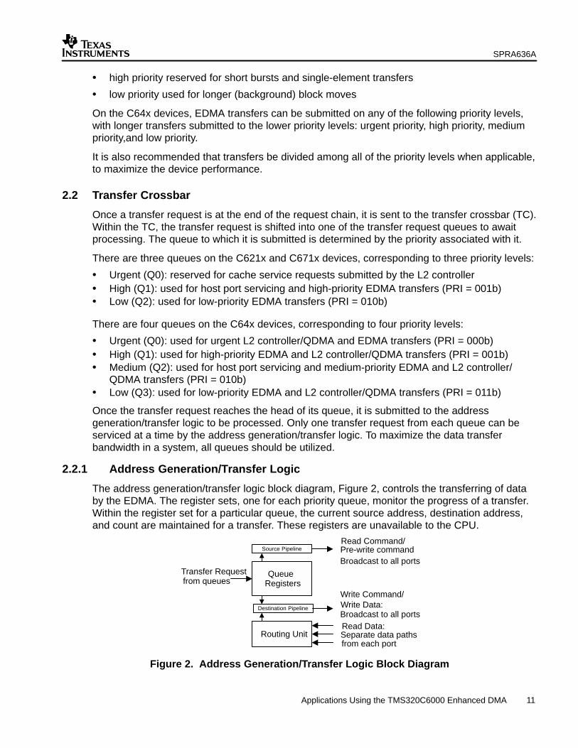
2.2.1 Address Generation/Transfer Logic
The address generation/transfer logic block diagram, Figure 2, controls the transferring of databy the EDMA. The register sets, one for each priority queue, monitor the progress of a transfer.Within the register set for a particular queue, the current source address, destination address,and count are maintained for a transfer. These registers are unavailable to the CPU.
QueueRegisters
Routing Unit
Read Command/Pre-write commandBroadcast to all ports
Write Command/Write Data:Broadcast to all portsRead Data:Separate data pathsfrom each port
12 Applications Using the TMS320C6000 Enhanced DMA
The queue registers essentially function as a traditional DMA. They maintain the transferparameters (source, destination, count, etc.) during the data transfer. The queue registers sendrequests for data to be transferred. These requests are for small bursts, which are less than orequal to the total data size of the submitted transfer request. The actual size depends on theport performing the data reads or writes and is fixed by the hardware to maximize performance.This allows transfers initiated by different queues to occur simultaneously to one another.Because the registers send requests for data transfers, the actual data movement occurs assoon as the ports are ready. Thus, if the different queues request transfers to/from differentports, then the transfers can occur at the same time. Transfer requests made to the same port(s)are arbitrated for priority.
Each queue register set submits its transfer request to the appropriate pipeline to initiate a datatransfer. There are three commands generated by the queue registers: pre-write, read, andwrite. Commands can be submitted to both pipelines once per cycle by any of the queueregisters. The TC arbitrates every cycle (separately for each pipeline) to allow the highestpriority command that is pending to be submitted. The pre-write command is issued to notify thedestination that it is going to receive data. All ports have a small buffer available to receive aburst of data at the internal clock rate. Once the destination has available space toaccommodate the incoming data, it sends an acknowledgement to the EDMA that it is ready.
After receiving the acknowledgement from the destination, a read command is issued to the datasource. Data is read at the maximum frequency of the source and passed to the EDMA routingunit to be sent to the destination.
Once the routing unit receives the data, the data is sent along with a write command to itsdestination.
Because the EDMA’s capability to wait for the destination to be ready to receive data, the sourceresource is free to be accessed for other transfers until the destination is ready. This provides anexcellent utilization of resources, and is referred to as write-driven processing. All commandsand write data are sent from the EDMA to all resources on a single bus. The information ispassed at the clock speed of the EDMA, and data from multiple transfers are interlaced whenoccurring simultaneously. Provided that multiple transfers (from different queues) have differentsources, the transfers occur simultaneously.
The read data arrives on unique buses from each resource. This is to prevent contention and toensure that data can be read at the maximum rate possible. Once the data arrives to the routingunit, the data that is available for the highest priority transfer is moved from its read bus to thewrite bus and sent to the destination.
2.3 EDMA Channel Parameters
EDMA channels are configured in a parameter table. The table is a 2-Kbyte block of on-chipparameter RAM (PaRAM) located within the EDMA. The table consists of 16 six-word parametersets (entries), one set per channel, for the C621x and C671x devices; and 64 six-wordparameter sets, one set per channel, for the C64x devices. The remaining PaRAM space isavailable for linked parameter sets for the channels. There is space for 69 (C621x and C671xdevices) or 21 (C64x devices) linked parameter sets. The last eight bytes of the PaRAM areunused (since 2 Kbytes are not evenly divisible by 24 bytes), but are accessible by the CPU andhost and can be used as a scratch area. The parameter RAM is listed in Table 2, parameter setsand options parameter register (OPT) are shown in Figure 3 and Figure 4, respectively.
SPRA636A
13 Applications Using the TMS320C6000 Enhanced DMA
Table 2. EDMA Channel Parameter RAM
Address Parameters
01A0 0000h to 01A0 0017h Parameters for event 0 (6 words)
01A0 0018h to 01A0 002Fh Parameters for event 1 (6 words)
01A0 0030h to 01A0 0047h Parameters for event 2 (6 words)
01A0 0048h to 01A0 005Fh Parameters for event 3 (6 words)
01A0 0060h to 01A0 0077h Parameters for event 4 (6 words)
01A0 0078h to 01A0 008Fh Parameters for event 5 (6 words)
01A0 0090h to 01A0 00A7h Parameters for event 6 (6 words)
01A0 00A8h to 01A0 00BFh Parameters for event 7 (6 words)
01A0 00C0h to 01A0 00D7h Parameters for event 8 (6 words)
01A0 00D8h to 01A0 00EFh Parameters for event 9 (6 words)
01A0 00F0h to 01A0 0107h Parameters for event 10 (6 words)
01A0 0108h to 01A0 011Fh Parameters for event 11 (6 words)
01A0 0120h to 01A0 0137h Parameters for event 12 (6 words)
01A0 0138h to 01A0 014Fh Parameters for event 13 (6 words)
01A0 0150h to 01A0 0167h Parameters for event 14 (6 words)
01A0 0168h to 01A0 017Fh Parameters for event 15 (6 words)
01A0 0180h to 01A0 0197h Parameters for event 16† (6 words)
01A0 0198h to 01A0 01AFh Parameters for event 17† (6 words)
... ...
... ...
01A0 05D0h to 01A0 05E7h Parameters for event 62† (6 words)
01A0 05E8h to 01A0 05FFh Parameters for event 63† (6 words)
01A0 0600h to 01A0 0617h Reload/link parameters for event N (6 words)
01A0 0618h to 01A0 062Fh Reload/link parameters for event M (6 words)
... ...
01A0 07E0h to 01A0 07F7h Reload/link parameters for event Z (6 words)
01A0 07F8h to 01A0 07FFh Scratch pad area (2 words)
† The C64x devices support up to 64 synchronization events. For the C621x/C671x device, these PaRAM locations (01A0 0180h - 01A005FFh) can be used for reload/link parameters.
SPRA636A
14 Applications Using the TMS320C6000 Enhanced DMA
31 16 15 0
Options (OPT) Word 0
Source Address (SRC) Word 1
Array/frame count (FRMCNT) Element count (ELECNT) Word 2
Destination address (DST) Word 3
Array/frame index (FRMIDX) Element index (ELEIDX) Word 4
Element count reload (ELERLD) Link address (LINK) Word 5
Figure 3. Parameter Storage for an EDMA Event
31 29 28 27 26 25 24 23 22 21 20 19 16
PRI ESIZE 2DS SUM 2DD DUM TCINT TCC
R/W-0 R/W-0 R/W-0 R/W-0 R/W-0 R/W-0 R/W-0 R/W-0
15 14 13 12 11 10 5 4 3 2 1 0
— TCCM� ATCINT� — ATCC� — PDTS� PDTD� LINK FS
R-0 R/W-0 R/W-0 R-0 R/W-0 R-0 R/W-0 R/W-0 R/W-0 R/W-0† Available only on C64x devices.Legend: R = Read only; W = Write only; R/W = Read/Write; -n = value after reset; — = reserved
Figure 4. EDMA Options Parameter Register
Each EDMA channel entry consists of several parameters that are used to configure the datatransfer. These parameters are described in Table 3.
Table 3. EDMA Channel Parameters
Offset Address†As defined for…
Offset Address†
(bytes) Parameter 1-D transfer 2-D transfer
0 Options Transfer configuration options.See Table 4.
Transfer configuration options.See Table 4.
4 Source address Address from which data is transferred. Address from which data is transferred.
8 Element count Number of elements per frame. Number of elements per array.
10 Frame count (1D),Array count (2D)
Number of frames per block minus 1. Number of arrays per frame minus 1.
12 Destination address Address to which data is transferred. Address to which data is transferred.
16 Element index Address offset of elements within aframe.
–––
18 Frame index (1D),Array index (2D)
Address offset of frames within a block. Address offset of arrays within a frame.
† The offset provided assumes little-endian mode of operation. All control registers are 32-bits wide, and the physical location of parameters thatshare a single register are fixed, regardless of endian mode. Control registers should always be accessed as 32-bit words. The specific offsetaddress entries that this note applies to are 8, 10, 16, 18, 20, and 22.
‡ This field is only valid for element-synchronized transfers.
SPRA636A
15 Applications Using the TMS320C6000 Enhanced DMA
Offset Address†
(bytes)
As defined for…
ParameterOffset Address†
(bytes) 2-D transfer1-D transferParameter
20 Link address PaRAM address containing theparameter set to be linked.
PaRAM address containing theparameter set to be linked.
22 Element count reload Count value to be loaded at the end ofeach frame.‡
–––
† The offset provided assumes little-endian mode of operation. All control registers are 32-bits wide, and the physical location of parameters thatshare a single register are fixed, regardless of endian mode. Control registers should always be accessed as 32-bit words. The specific offsetaddress entries that this note applies to are 8, 10, 16, 18, 20, and 22.
‡ This field is only valid for element-synchronized transfers.
The options parameter (Figure 4) is made up of several fields that determine the way in whichdata is arranged in memory, as well as the way in which the data is transferred. The C64xdevices have five additional fields in the option register as a result of it’s enhanced features. Allof these fields are described in Table 4.
Table 4. EDMA Channel Options Field Values
Field Value Description
PRI Priority levels for EDMA events.
For C621x and C671x only:
000 Reserved. Urgent priority level reserved for cache servicing. Not valid for EDMA transfer requests.
001 High priority EDMA transfer. Transfer requests submitted to Q1.
010 Low priority EDMA transfer. Transfer requests submitted to Q2.
011-111 Reserved
For C64x only:
000 Urgent priority.
001 High priority EDMA transfer.
010 Medium priority EDMA transfer.
011 Low priority EDMA transfer.
100-111 Reserved
ESIZE Element size.
00 32-bit element (word)
01 16-bit element (half-word)
10 8-bit element (byte)
11 Reserved
2DS Source dimension.
SPRA636A
16 Applications Using the TMS320C6000 Enhanced DMA
Table 4. EDMA Channel Options Field Values (Continued)
DescriptionValueField
0 1-dimensional source
1 2-dimensional source
SUM Source address update mode.
00 Fixed address mode. No source address modification.
01 Source address increment depends on 2DS and FS bits.
10 Source address decrement depends on 2DS and FS bits.
11 Source address modified by the element index/frame index depending on 2DS and FS bits.
2DD Destination dimension.
0 1-dimensional destination
1 2-dimensional destination
DUM Destination address update mode.
00 Fixed address mode. No destination address modification.
01 Destination address increment depends on 2DD and FS bits.
10 Destination address decrement depends on 2DD and FS bits.
11 Destination address modified by the element index/frame index depending on 2DD and FS bits.
TCINT Transfer complete interrupt.
0 Transfer complete indication is disabled. CIPR bits are not set upon completion of a transfer.
1 CIPR bit is set on channel transfer completion. The bit (position) set in the CIPR is specified by the TCCvalue.
TCC 0–1111 Transfer complete code. This 4-bit value (0–15) is used to set the bit in CIPR (CIPR[TCC] bit) providedTCINT = 1, when the current set is exhausted. For C64x, TCC works in conjunction with TCCM to providea 6-bit transfer complete code.
TCCM 0–11 For C64x only: Transfer complete code most-significant bits. TCCM works in conjunction with TCC toprovide a 6-bit transfer complete code. The 6-bit code is used to set the relevant bit in CIPRL or CIPRHprovided TCINT = 1, when the current set is exhausted.
ATCINT For C64x only: Alternate transfer complete interrupt.
0 Alternate transfer complete indication is disabled. CIPR bits are not set upon completion of intermediatetransfers in a block.
1 The CIPR bit is set upon completion of intermediate transfers in a block. The bit (position) set in the CIPRis the ATCC value specified.
ATCC 0–111111
For C64x only: Alternate transfer complete code. The 6-bit value (0–63) is used to set the bit in CIPRLor CIPRH (CIP[ATCC] bit) provided ATCINT = 1, upon completion of an intermediate transfer in a block.
PDTS For C64x only: Peripheral device transfer (PDT) mode for source.
SPRA636A
17 Applications Using the TMS320C6000 Enhanced DMA
Table 4. EDMA Channel Options Field Values (Continued)
DescriptionValueField
0 PDT read is disabled.
1 PDT read is enabled.
PDTD For C64x only: Peripheral device transfer (PDT) mode for destination.
0 PDT write is disabled.
1 PDT write is enabled.
LINK Linking of event parameters enable.
0 Linking of event parameters is disabled. Entry is not reloaded.
1 Linking of event parameters is enabled. After the current set is exhausted, the channel entry is reloadedwith the parameter set specified by the link address. The link address must be on a 24-byte boundaryand within the EDMA PaRAM. The link address is a 16-bit address offset from the PaRAM base address.
FS Frame synchronization.
0 Channel is element/array synchronized.
1 Channel is frame/block synchronized.
2.4 QDMA Parameters
The EDMA also has the capability of performing unsynchronized transfers through the use of aQDMA request by the CPU. The QDMA is used to issue single, independent transfers to quicklymove data, rather than to perform periodic or repetitive transfers like the EDMA channels.
Since the QDMA is used for quick, one-time transfers it does not have the capability to reload acount or link. The count reload/link address register is, therefore, not available to the QDMA.The QDMA can be used for chaining transfers, which is described later in this document. TheQDMA registers are not updated during or after a transfer by the hardware. They retain thevalues that were submitted.
The QDMA consists of two sets of memory-mapped, write-only registers, as shown inFigure 5(a). The first set is a direct mapping of the five QDMA registers required to configure atransfer. There is no count reload, no link address, and the LINK field (bit 1) of the optionsparameter, Figure 5(b), is reserved. Writing to these registers configures, but does not submit, aQDMA transfer request.
SPRA636A
18 Applications Using the TMS320C6000 Enhanced DMA
(a) QDMA registers and QDMA pseudo-registers
0200 0000h QDMA Options (OPT) QDMA Registers
Source Address (SRC)
Array/frame count (FRMCNT) Element count (ELECNT)
Destination address (DST)
0200 0010h Array/frame index (FRMIDX) Element index (ELEIDX)
PRI ESIZE 2DS SUM 2DD DUM TCINT TCC — TCCM� reserved FS
W-0 W-0 W-0 W-0 W-0 W-0 W-0 W-0 0 W-0 0 1
† Available only on C64x devices.Legend: W = Write only; -n = value after reset; — = reserved
Figure 5. QDMA Registers
The second register set is a pseudo-mapping of the QDMA registers, and is available to enablemore efficient transfer request submission by the CPU. Writing to any one of thepseudo-registers not only configures the selected register but also submits a transfer request.
A QDMA transfer requires only one to five cycles to submit, depending on the number ofregisters that need to be configured. A typical QDMA transfer is performed by writing four of theparameter values to their registers followed by the write of the fifth parameter to itscorresponding pseudo-register. All QDMA transfers are submitted using frame synchronization;therefore, the QDMA always requests a transfer of one complete frame of data. Only onerequest is sent for any QDMA submission, and the number of elements transferred is shown inTable 5.
Table 5. QDMA Transfer Length
Transfer Dimension Elements Transferred
1-D to 1-D One frame, regardless of frame count
Other One frame, all arrays transferred
SPRA636A
19 Applications Using the TMS320C6000 Enhanced DMA
All of the QDMA registers retain their value after the request is submitted, so if a second transferis to be performed with any of the same parameter settings, they do not need to be rewritten bythe CPU. Only the changed registers must be rewritten, with the final parameter written to theappropriate pseudo-register to submit the transfer.
2.5 Synchronization
In the C621x and C671x devices, all EDMA channels are tied to a specific synchronizationevent. In the C64x devices, some EDMA channels are tied to a specific synchronization eventand some EDMA channels are not. A channel requests a data transfer only when it receives itsevent, is chained to or from another channel, or when the CPU synchronizes it manually (bywriting to the ESR). The amount of data to be transferred depends on the channel’sconfiguration. A channel can submit an entire frame when frame synchronized or can submit asubset of a frame (element or array, depending on dimension) whenelement/array synchronized. Even the QDMA is synchronized, with its event being a CPU storeto one of its pseudo-registers.
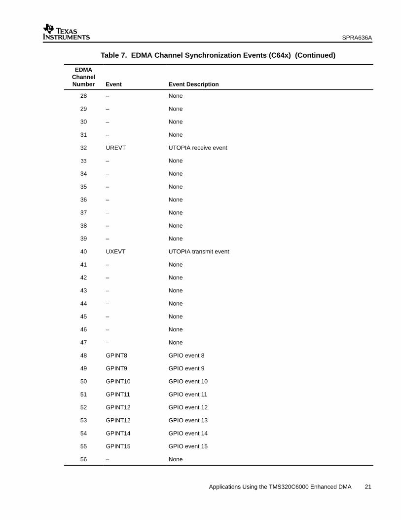
Table 6 and Table 7 list the synchronization events associated with each of the programmableEDMA channels.
Table 6. EDMA Channel Synchronization Events (C621x and C671x)
EDMAChannelNumber Event Event Description
0 DSPINT Host-to-DSP interrupt
1 TINT0 Timer 0 interrupt
2 TINT1 Timer 1 interrupt
3 SD_INT SDRAM timer interrupt
4 EXT_INT4 External interrupt pin 4
5 EXT_INT5 External interrupt pin 5
6 EXT_INT6 External interrupt pin 6
7 EXT_INT7 External interrupt pin 7
8 EDMA_TCC8 Any QDMA/EDMA channel with TCC = 1000b
9 EDMA_TCC9 Any QDMA/EDMA channel with TCC = 1001b
10 EDMA_TCC10 Any QDMA/EDMA channel with TCC = 1010b
11 EDMA_TCC11 Any QDMA/EDMA channel with TCC = 1011b
12 XEVT0 McBSP0 DXR-to-XSR copy
13 REVT0 McBSP0 RBR-to-DRR copy
14 XEVT1 McBSP1 DXR-to-XSR copy
15 REVT1 McBSP1 RBR-to-DRR copy
SPRA636A
20 Applications Using the TMS320C6000 Enhanced DMA
Element/array synchronization means that for each synchronization event received, onesubframe is transferred. A subframe is the number of elements defined by the second dimensionof a particular transfer: a single element (for 1-D transfers) or an array of elements (for 2-Dtransfers).
2.5.2 Frame/Block Synchronization
Frame/block synchronization means that for each synchronization event received, an entireframe/block is transferred. For 1-D transfers, this is a frame of elements; for 2-D transfers, this isa frame of arrays (block).
2.6 Dimensioned Transfers
Transfers performed by the EDMA have dimension: either one-dimensional (1-D) ortwo-dimensional (2-D). The 1-D transfers correspond to those performed by traditional DMAslike that of the TMS320C6201 DSP. The 2-D transfers allow additional functionality notpreviously available.
The number of dimensions a transfer has determines the makeup of a frame/block of data. In a1-D transfer, frames are made up of a number of individual elements. In a 2-D transfer, blocksare made up of a number of arrays, each of which is made up of a number of elements.
2.6.1 1-D Transfers
One-dimensional transfers focus on individual elements. Each frame of data to be transferred isassociated with a single dimension that indicates the number of elements per frame. EDMAchannels may be configured to transfer multiple frames (or a block of frames), but each frame ishandled individually. A 1-D transfer can be considered two dimensional, with the seconddimension fixed at 1. A sample 1-D frame is shown in Figure 6, with an element count of n.
1 2 3 n... ...
n elements per frame
Figure 6. 1-D Transfer Data Frame
SPRA636A
23 Applications Using the TMS320C6000 Enhanced DMA
The elements within a frame can be all located at the same address, at contiguous addresses,or at a configurable offset from one another. The addresses of elements within a frame can belocated at a specific distance apart (determined by element index, EIX), while the address of thefirst element of each frame is a set distance from a particular element of the previous frame(determined by frame index, FIX).
The value of the frame index (FIX) depends on the synchronization mode of the transfer.Transfers may be submitted as one of the following:
• one element at a time—when element synchronized
• one frame at a time—when frame synchronized
2.6.2 2-D Transfers
Two-dimensional transfers assume a slightly different arrangement of elements. Each block ofdata to be transferred has two dimensions: the number of arrays within the block, and thenumber of elements within an array. Elements within an array are contiguous, and arrays areoffset from one another by a fixed amount. A sample 2-D block is shown in Figure 7, with anarray count of n and an element count of m.
0_1 ... ...0_2 0_3 0_m
1_1 ... ...1_2 1_3 1_m
2_1 ... ...2_2 2_3 2_m
m elements per array
n + 1arrays
perframe
: : :: : :
n_1 ... ...n_2 n_3 n_m
Figure 7. 2-D Transfer Data Block
The offset of the arrays is determined by the array index (AIX). The value of the array indexdepends on the synchronization mode of the transfer. Transfers may be submitted as one of thefollowing:
• one array at a time—when array synchronized
• one frame at a time—when block synchronized
2.7 Address Updates
The relative addresses of the elements to be transferred by the EDMA are configurable withineach channel’s parameter set, and are based on the settings of the source and destinationaddress update modes (SUM and DUM, respectively). The update modes determine how theelements are arranged in memory. The data elements can be at the same memory address, atcontiguous memory addresses, or at a specified offset from one another using programmableindex values. Table 8 gives the possible address update modes for a transfer.
SPRA636A
24 Applications Using the TMS320C6000 Enhanced DMA
Table 8. Address Update Modes
SUM/DUM 1-D 2-D
00: No modification All elements located at the same address. All elements in an array are at the sameaddress.
01: Increment All elements are contiguous, with subsequentelements located at a higher address than theprevious.
All elements within an array are contiguous,with subsequent elements located at a higheraddress than the previous. Arrays are offsetby AIX.
10: Decrement All elements are contiguous, with subsequentelements located at a lower address than theprevious.
All elements within an array are contiguous,with subsequent elements located at a loweraddress than the previous. Arrays are offsetby AIX.
11: Index All elements within a frame are offset fromone another by EIX. Frames are offset by FIX.
Reserved
The indexes described in the table (EIX, FIX, and AIX) have slightly different connotationsdepending on the synchronization of a channel. In order to understand what value the indexmust have, it is important to know where the address update is to take place. Address updatescan occur in two places:
• within the parameter set of an EDMA channel
• within the address generation/transfer logic
Within the parameter table, the addresses are updated following the submission of each transferrequest. The starting address of a transfer request is based on the starting address of theprevious submission. The address generation/transfer logic manages the address updateswithin a burst —the address of each element being based on the address of the previouselement.
If a channel is configured to be an element-synchronized 1-D transfer, then the source anddestination addresses are updated within the parameter table following the transfer requestsubmission for each element. Therefore, the element index (EIX) and frame index (FIX) shouldbe based on the difference between element addresses, as shown in Figure 8.
A B C D
E F G H
I J K L
EIX
FIX
FIX
EIX EIX
One elementtransferred per
sync event
Figure 8. 1-D Transfer With Element Synchronization
SPRA636A
25 Applications Using the TMS320C6000 Enhanced DMA
A channel that is configured to perform a 2-D transfer with array synchronization updates itssource and destination registers after the transfer request for each array is submitted. The arrayindex (AIX) is the difference between the starting addresses for each array of the block, asshown in Figure 9.
A CB D
E GF H
I KJ L
AIX
AIX
One arraytransferred per
sync event
Figure 9. 2-D Transfer With Array Synchronization
Frame/block synchronization allows a channel to request the transfer of an entire frame ofelements or block of arrays. For a 1-D transfer, this means that the frame index (FIX) no longerrepresents the difference between the address of the last element of a frame and the address ofthe first element of the subsequent frame, but rather the difference between the startingaddresses of each frame. A frame-synchronized 1-D transfer is functionally identical to anarray-synchronized 2-D transfer (assuming EIX equals the number of bytes per element). Forreference:
frame-synchronized 1-D transfer = array-synchronized 2-D transfer(where EIX = number of bytes per element)
The address indexing for a frame-synchronized 1-D transfer is shown in Figure 10.
A B C D
E F G H
I J K L
EIX
FIX
FIX
EIX EIX
One frametransferred per
sync event
Figure 10. 1-D Transfer With Frame Synchronization
SPRA636A
26 Applications Using the TMS320C6000 Enhanced DMA
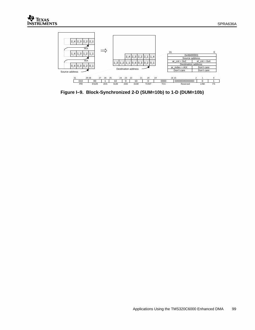
For a 2-D transfer, block synchronization causes the array index (AIX) to be implemented by theaddress generation/transfer logic. The address is updated after each element in a burst. Thelogic first updates the addresses according to the setting of SUM/DUM. If an element is the lastin a particular array and an update mode is selected (SUM/DUM ≠ 00b), the address(es) areindexed according to AIX. AIX is added to the address after the address update occurs. AIX isequal to the space between arrays of a block, as shown in Figure 11.
A CB D
E GF H
I KJ L
AIX
AIX
One blocktransferredper sync
event
Figure 11. 2-D Transfer With Block Synchronization
2.8 Transfer Linking
An important capability of the EDMA is that of linking. Linking is an enhancement beyond theautoinitialization feature of the C6201 DMA. By providing a link address and setting LINK = 1 inthe transfer options, an EDMA channel loads a new entry from PaRAM and begins performingthe new transfer. The linked list is traversed until LINK = 0. If the linked list is a closed loop, theEDMA channel runs continuously throughout the DSP operation. A sample of a linked list isshown in Figure 12.
Options (LINK = 1)Source address
Destination addressArray/Frame count Element count
Array/Frame index Element indexCount reload Link address (A)
Options (LINK = 1)Source address
Destination addressArray/Frame count Element count
Array/Frame index Element indexCount reload Link address (B)
Options (LINK = 1)Source address
Destination addressArray/Frame count Element count
Array/Frame index Element indexCount reload Link address (C)
Destination addressArray/Frame count Element count
Array/Frame index Element indexCount reload Don’t care
EDMA reload parameters (C)
Figure 12. EDMA Linked List of Transfers
Linking an entry to itself replicates the behavior of autoinitialization to facilitate the use of circularbuffering and repetitive transfers. After an EDMA channel exhausts its current entry, theparameter set is reloaded and the transfer begins again.
Linking also provides the ability to string several entries together, such that multiple transfers areperformed using the same synchronization event. This is a useful feature for managing multipledata buffers for incoming/outgoing data (such as in a ping-pong buffer scheme) and performingcontinuous transfers. After an EDMA channel exhausts its current entry, the next parameter setis loaded and begun.
SPRA636A
27 Applications Using the TMS320C6000 Enhanced DMA
Since each channel is capable of linking together a list of transfers, it is often possible toinitialize all of the transfers that are required throughout system operation at once. This removesthe overhead associated with reprogramming a DMA channel.
2.9 Transfer Chaining
In the C621x and C671x devices, four of the EDMA channels are synchronized upon thecompletion of transfers by other channels. In the C64x devices, all EDMA channels can beprogrammed to be synchronized upon the completion of transfers by other channels. Thisfunctionality corresponds to the synchronization of a channel in the C6201 DMA to an interruptby another channel. Through the use of a transfer completion code (TCC), any EDMA channel(or a QDMA transfer) can synchronize any of these channels. This is referred to as chaining.
In the C621x and C671x devices, EDMA channels 8 through 11 are used for chaining and aresynchronized by TCC values 8 (1000b) through 11 (1011b). In the C64x devices, all EDMAchannels (0–63) can be used for chaining and are synchronized by TCC values 0 (00 0000b)through 63 (11 1111b). The C64x devices contain two additional TCC bits than the other devicesto allow support for all 64 channels. In addition, C64x devices allow for alternate transfercomplete chaining. When this is enabled, the next EDMA channel (specified by the ATCC of thecurrent channel) is synchronized upon completion of each intermediate transfer of the currentchannel. Alternate transfer complete chaining is useful for such applications as servicinginput/output FIFOs with a single event and breaking up large transfers. It is important to notethat alternate transfer complete chaining is not applicable to block-synchronized 2-D transfersand is superceded by transfer complete chaining upon completion of the entire transfer. Toenable chaining functionality, the EDMA channel whose transfer completion triggers the chainedtransfer must have both:
• TCC set to the appropriate value
• TCINT bit of the options field set to 1
and/or (C64x only):
• ATCC set to the appropriate value
• ATCINT bit of the options field set to 1
The chaining functionality must also be enabled. Since TCC values are not restricted to chainingonly, the chaining enable is separate from the event enable. This allows a channel to report aTCC value without synchronizing the corresponding channel, while still allowing these channelsto be used. These channels could be used with manual synchronization while another channelreports a TCC value corresponding to these channels without conflict by not enabling chaining.Setting the appropriate bits in the channel chain enable register (CCER) enables chaining.
By using the chaining functionality, several things are possible:
• An EDMA transfer can be synchronized by the completion of another EDMA transfer toallow sequential transfers to be performed based on a single event. For example, use anEDMA channel to receive a frame of input data, then automatically trigger an output frame ofdata to be transferred immediately afterward.
SPRA636A
28 Applications Using the TMS320C6000 Enhanced DMA
• An EDMA channel can synchronize itself to traverse through its linked listautomatically. For example:
if... then...
Multiple entries are linked together on one ofthe channels available for chaining AND... Each entry provides a TCC value equal to itschannel number
Each entry will submit a transfer request assoon as the previous completes. Valid only ifeach entry exhausts its full parameter setupon submission.
This is a way to perform complicated transfers based on a single event (either by the CPU,QDMA, or another EDMA channel).
2.10 C64x DSP Advanced Features
The C64x EDMA has many advanced features not found in the C621x/C671x EDMA. The C64xhas 64 channels, allows transfer chaining on all channels, and allows L2 controller transfers andEDMA transfers on all four priority levels. In addition, the C64x devices support PeripheralDevice Transfers, event polarity selection, Alternate Transfer Complete Chaining and Interrupt,and have programmable queue lengths and readable QDMA registers. Information on all ofthese advanced features can be found in the TMS320C6000 Peripherals Reference GuideSPRU190.
3 CPU Interrupt Service RoutinesThere is one interrupt from the EDMA to the CPU, EDMA_INT, which can be triggered by any ofthe EDMA channels or the QDMA. A channel interrupt is passed to EDMA_INT when enabled inthe channel interrupt enable register (CIER). If the CIE bit is set for a particular TCC, thenEDMA_INT is set when this code is received. The CPU then branches to the correspondinginterrupt vector, providing that a CPU interrupt is configured for EDMA_INT and is enabled. 1
A TCC is issued when provided by a QDMA/EDMA channel transfer request, along with TCINTset to 1. Providing a TCC value and setting the TCINT bit enables a channel to signal to theEDMA controller that it has completed its transfer. This causes a flag to be set in the channelinterrupt pending register (CIPR). The bit that is set is determined by the TCC configured in thechannel options. The CPU must manually clear the CIPR.
To configure the EDMA for any channel (or QDMA request) to interrupt the CPU:
• Set CIEn to 1 in the CIER
• Set TCINT to 1 in channel options
• Set TCC to n in channel options
Anytime a TCC is reported after a completed transfer, the CPU is interrupted. More than oneQDMA/EDMA channel can use the same TCC value, and the TCC value is not required to beequal to the channel number.
Since all EDMA channels and the QDMA share the same CPU interrupt, the CPU must poll theCIPR to determine the interrupt source. One possible ISR is shown in Figure 13 (C621x andC671x devices) and in Figure 14 (C64x devices). The ISR clears the CIP bits and branches to aC routine for a particular channel.
1. See the TMS320C6000 Peripherals Reference Guide (SPRU190) and the TMS320C6000 CPU and Instruction Set Reference Guide (SPRU189) for chapters on configuring CPU interrupts.
SPRA636A
29 Applications Using the TMS320C6000 Enhanced DMA
// C621x/C671x EDMA interrupt service routine
// Service all pending EDMA interrupts. In this ISR, the highest
// priority interrupt that is pending is isolated, and the routine
channel_num = 63 – _lmbd(1, mask_high); // Get high–pri ch num
EDMA_RSET(CIPRH, mask_high); // Clear CIP from CIPRH
CIPRH_val ^= mask_high; // Clear from CIPRH_val
}
if (channel_num >= 0){ // If valid channel
EDMA_CH_ISR(channel_num); // Service high–pri ch
}
} // End while
} while (IRQ_test(IRQ_EVT_EDMAINT)); // Poll IFR for new
} // End EDMA_INT_ISR
Figure 14. C64x EDMA Interrupt Service Routine
Some special considerations must be made for an ISR that services multiple interrupts. The ISRshown in Figure 13 and Figure 14 addresses the following concerns:
• Multiple sources generate EDMA_INT
SPRA636A
31 Applications Using the TMS320C6000 Enhanced DMA
• The ISR does not know the interrupt source prior to execution
• New EDMA interrupts can be generated during ISR
Because multiple EDMA channels can trigger the same interrupt, it should be assumed that anew EDMA interrupt can occur in the time between the CPU interrupt flag being cleared and theCIPR being read within the ISR (the interrupt flag is cleared when the branch is taken to theinterrupt vector). If a new EDMA interrupt is received during that time, the CPU services itwithout clearing the interrupt flag. This results in an additional CPU delay caused by branchingback to the main code body and immediately returning to the ISR for an interrupt that hasalready been serviced. By checking for a new CPU flag posting at the end of the ISR, the CPUknows if additional events have been received.
4 Transfer Examples
A wide variety of transfers can be performed by the EDMA depending on the parameterconfiguration. Basic transfers can be performed either by an EDMA channel or by submitting aQDMA. Complicated transfers or repetitive transfers require an EDMA channel to be used.
4.1 Block Move Examples
The most basic transfer performed by the EDMA is that of a block move. Often during deviceoperation it is necessary to transfer a block of data from one location to another, usuallybetween on- and off-chip memory.
In this example, a section of data is to be copied from external memory to internal L2 SRAM.The data block is 256 words and resides at address 8000 0000h (CE0). It is to be transferred tointernal address 0000 8000h (L2 cache). The data transfer is shown in Figure 15.
8000 0000h 0000 8000h
......
......
255254253
7654321 8
1514131211109 16
20191817 21
247246245244 248
252251250249 256
......
......
255254253
7654321 8
1514131211109 16
20191817 21
247246245244 248
252251250249 256
Figure 15. Block Move Diagram
The fastest way to perform this transfer is through a QDMA request. The QDMA request can besubmitted in several different ways, the most basic being a frame-synchronized 1-D to 1-Dtransfer. This type of transfer is valid for block sizes of less than 64K elements. The transfermust be frame-synchronized so that all of the elements are transferred once the entry issubmitted. If the transfer were to be configured as an element-synchronized transfer, only thefirst element would be transferred.
The register parameters for this block move transfer are shown in Figure 16. Parameters thatmust be configured are: QDMA options, source address, destination address, and elementcount.
SPRA636A
32 Applications Using the TMS320C6000 Enhanced DMA
Register Contents Register
8000 0000h QDMA Source Address Register
0000h 0100h QDMA (Array/Element) Transfer Count Register
0000 8000h QDMA Destination Address Register
Don’t care Don’t care QDMA (Array/Element) Index Register
PRI ESIZE 2DS SUM 2DD DUM TCINT TCC — TCCM� reserved FS
† Available only on C64x devices.
Figure 16. Block Move QDMA Register Parameters
The source address for the QDMA is set to the start of the data block in external memory, andthe destination address is set to the data block in L2. Since all data is contiguous, SUM andDUM are both set to 01b (increment). The priority is set to 001b to indicate a high-prioritytransfer. The block move request is submitted to the high-priority queue (Q1).
The CPU requires four cycles to submit the request for this transfer, one cycle for each registerwrite.2 Three of the QDMA parameters must be written to their proper QDMA registers, and oneparameter must be written to its pseudo-register, which initiates the transfer. A sample QDMAsubmission for the above transfer is:
…EDMA_RSET(QDMA_SRC, 0x80000000); /* Set source address */
EDMA_RSET(QDMA_DST, 0x00008000); /* Set destination address */
EDMA_RSET(QDMA_CNT, 0x00000100); /* Set frame/element count */
EDMA_RSET(QDMA_S_OPT, 0x21200001); /* Set options and submit */
…
A block that contains greater than 64k elements requires the use of both element count andarray/frame count. Since the element count field is only 16 bits, the largest count value that canbe represented is 65535. Any count larger than this needs to be represented with an array countas well. In order to transmit this amount of data, a QDMA can still be used. Rather than aframe-synchronized 1-D to 1-D transfer, the QDMA needs to be configured as ablock-synchronized 2-D to 2-D transfer.
2. Fewer cycles are required if any of the QDMA registers are already configured. A minimum of one cycle is required.
SPRA636A
33 Applications Using the TMS320C6000 Enhanced DMA
4.2 Subframe Extraction Examples
The EDMA has an efficient way of extracting a small frame of data from a larger one. Byperforming a 2-D to 1-D transfer, the EDMA can retrieve a portion of data for the CPU toprocess. In this example, a 640 x 480-pixel frame of video data is stored in external memory,CE2. Each pixel is represented by a 16-bit halfword. A 16 x 12-pixel subframe of the image isextracted for processing by the CPU. To facilitate more efficient processing time by the CPU, theEDMA places the subframe in internal L2 SRAM. Figure 17 shows the transfer of the subframefrom external memory to L2.
To perform this transfer, the CPU can issue a QDMA request for a frame-synchronized 2-D to1-D transfer. Since the source is 2-D and the transfer is block-synchronized, the QDMA requestsa transfer of the entire subframe. The parameters required for the QDMA registers to requestthis transfer are shown in Figure 18.
Register Contents Register
A000 0788h QDMA Source Address Register
000Bh 0010h QDMA (Array/Element) Transfer Count Register
0000 2000h QDMA Destination Address Register
04E0h Don’t care QDMA (Array/Element) Index Register
34 Applications Using the TMS320C6000 Enhanced DMA
All of the address updates occur within the address generation/transfer logic. The array indexprovided is therefore the space between arrays of the subframe. Since each array of the videoimage is 640 pixels in length and each array of the subframe is 16 pixels in length, the arrayindex is set to:
2 bytes/element * (640 – 16) elements = 1248 bytes
The subframe is transferred to a block of contiguous memory. The element count is set to 16,the number of elements per subframe array, and the frame count is set to 11, one less than thenumber of arrays. The QDMA request is sent to the low–priority queue, Q2, so that it does notinterfere with any data acquisition that could be occurring.
Inversely, a 1-D to 2-D transfer can be used to perform the insertion of a subframe into a largerframe of data. For instance, with this example the subframe could be inserted back into thelarger image after some processing by the CPU.
4.3 Data Sorting Examples
Many applications require the use of multiple data arrays. It is often desirable to have the arraysarranged so that the first elements of each array are adjacent, the second elements areadjacent, and so on. Often this is not the format in which the data is presented to the device.Either data is transferred via a peripheral, with the data arrays arriving one after the other, or thearrays are located in memory, with each array occupying a portion (frame) of contiguousmemory spaces. For these instances, the DMA can be configured to reorganize the data into thedesired format. Figure 19 shows the data sorting of element arrays.
A_1023
...
...
A_3
A_2
A_1
A_1024
B_1023
...
...
B_3
B_2
B_1
B_1024
C_1023
...
...
C_3
C_2
C_1
C_1024
D_1023
...
...
D_3
D_2
D_1
D_1024
8000 0000h
0000 8000h
A_1023
......A_3
A_2
A_1
A_1024
B_1023
......B_3
B_2
B_1
B_1024
C_1023
......C_3
C_2
C_1
C_1024
D_1023
......D_3
D_2
D_1
D_1024
A_1022
B_1022
C_1022
D_1022
A_1022
B_1022
C_1022
D_1022
Figure 19. Data Sorting Example Diagram
The following values can be used to determine the fields required to use QDMA requests toorganize the data in memory by ordinal position:
• F = The initial value of Frame Count
• E = The initial value of Element Count, as well as the Element Count Reload value
• S = The element size in bytes
The QDMA can again be used to transfer this data. However, due to the arrangement of the datain the destination, it is not possible to accomplish this with a single submission. Instead aseparate QDMA transfer request must be submitted for each frame. If it is necessary to use anEDMA channel to perform this transfer, then an entry must be provided for each frame in thetransfer in PaRAM. Also, the transfer must use the chaining feature to self–synchronize eachframe on the completion of the previous (only channels 8–11 on C621x/C671x devices). SeeTransfer Chaining, section 2.9, for details.
SPRA636A
35 Applications Using the TMS320C6000 Enhanced DMA
This example focuses on the second case mentioned previously, in which data arrays of equalsize are located in external memory. It is not necessary for the arrays to be of equal length. Inthe case that the lengths vary, each QDMA submission or each EDMA reload parameter set inPaRAM would contain the corresponding new count value.
For this example, it is assumed that the 16-bit data is located in external RAM, beginning ataddress A000 0000h (CE2). The QDMA is used to bring four frames of 1k half-words from theirlocations in RAM to internal data memory beginning at 0000 8000h. The index value required isEIX = F × S = 4 × 2 = 8.
Since separate QDMA transfer requests are to be submitted for each frame, only the EIX valueis used in the QDMA parameters. The CPU updates the destination address for each newframe. For the first frame of data, the values shown in Figure 20 must be assigned to the QDMAregisters.
Register Contents Register
A000 0000h QDMA Source Address Register
Don’t care 0400h QDMA (Array/Element) Transfer Count Register
0000 8000h QDMA Destination Address Register
Don’t care 0008h QDMA (Array/Element) Index Register
PRI� ESIZE 2DS SUM 2DD DUM TCINT TCC — TCCM‡ reserved FS
† Program to 011 on C64x devices.‡ Available only on C64x devices.
Figure 20. Sorting QDMA Register Parameters
The QDMA, submitted with the parameters shown in Figure 21, only transfers the first frame. Foreach subsequent frame, the CPU must perform two stores to change the source address andthe destination address manually. It is not necessary for the CPU to wait for each frame tocomplete before submitting a request for the next. The subsequent transfer requests submittedare stored in the transfer queues to await processing.
To summarize, the CPU performs four writes to configure the options field, the source address,the count, and the destination address (or any four of the five fields). The CPU then performs awrite to the index pseudo–register (or the register still not configured) to submit the transferrequest for the first frame. For each additional frame, the CPU increments the source address byE × S (1024 × 2 = 2048) and stores this value to the source address register. The CPU alsoincrements the destination address by S and stores this value to the destination addresspseudo–register to submit the transfer request.
If it is desired to have the EDMA notify the CPU when all of the transfers have completed, thenthe transfer request for the last frame should also have a modified options field to include a TCCvalue (and have TCINT = 1). See CPU Interrupt Service Routines, section 3, for details on this.
SPRA636A
36 Applications Using the TMS320C6000 Enhanced DMA
4.4 Peripheral Servicing Examples
An important capability of the EDMA is its ability to service peripherals (in the background ofCPU operation) without requiring any CPU intervention. Through proper initialization of theEDMA channels, they can be configured to continuously service on- and off-chip peripheralsthroughout the device operation. Each event available to the EDMA has its own dedicatedchannel, and all channels operate simultaneously. This means that all data streams can behandled independently with little or no consideration for what else is going on in the EDMA.
Since all EDMA channels are always synchronized, there are no special setups required toconfigure a channel to properly service a particular event. The only requirements are to use theproper channel for a particular transfer and to enable the channel’s event in the EER or CCER(unless the CPU synchronizes the channel).
When programming an EDMA channel to service a peripheral, it is necessary to know how datais to be presented to the DSP. Data is always provided with some kind of synchronization event,and is either one element per event (non-bursting), or multiple elements per event (bursting).
4.4.1 Nonbursting Peripherals
Non-bursting peripherals include the on-chip McBSPs and many external devices such ascodecs. Regardless of the peripheral, the EDMA channel configuration is the same.
The on-chip McBSPs are the most commonly used peripherals in a C6000 system. EDMAchannels 12 and 13 are dedicated to McBSP0 transmit and receive events, and channels 14 and15 are dedicated to McBSP1 transmit and receive events. In addition, the C64x devices dedicatechannels 17 and 18 to McBSP2 transmit and receive events. The transmit and receive datastreams are treated independently by the EDMA. While a standard DMA channel could be usedin split-mode to handle transmit and receive data, there are a number of restrictions with thisbecause of the sharing of resources. The EDMA channels do not have these restrictions.Although most serial applications call for similar data formats both to and from the McBSP, this isnot a requirement for reliable operation with the EDMA. The transmit and receive data streamscan have completely different counts, data sizes, and formats.
If the previous block move example were changed so that the 256 words were received byMcBSP0 to be transferred to internal L2 SRAM, the transfer would easily be handled by EDMAchannel 13, which is synchronized by REVT0. Figure 21 shows a block diagram of this transfer.
3000 0000h
0000 2000h
......
......
255254253
7654321 8
1514131211109 16
20191817 21
247246245244 248
DRRRBRRSR
REVT01:
2
:
3
:
252251250249 256
Figure 21. McBSP Servicing for Incoming Data
SPRA636A
37 Applications Using the TMS320C6000 Enhanced DMA
To transfer the incoming data stream to its proper location in L2 memory, the EDMA channelmust be set up for a 1-D to 1-D transfer with element synchronization. Since an event (REVT0)is generated for every word as it arrives, it is necessary to have the EDMA issue the transferrequest for each element individually. The channel entry for this transfer is shown in Figure 22.
Register Contents Register
3000 0000h EDMA Source Address Register
0000h 0100h EDMA (Frame/Element) Transfer Count Register
0000 2000h EDMA Destination Address Register
Don’t care Don’t care EDMA (Frame/Element) Index Register
Don’t care NULL set EDMA Count Reload/Link Address Register
2020 0002h EDMA Options Register
⇓
31 29 28 27 26 25 24 23 22 21 20 19 16
001 0 0 0 00 0 01 0 0000
PRI ESIZE 2DS SUM 2DD DUM TCINT TCC
15 14 13 12 11 10 5 4 3 2 1 0
0 00 0 0 000 000 0 0 0 1 0
— TCCM� ATCINT� — ATCC� — PDTS� PDTD� LINK FS
† Available only on C64x devices.
Figure 22. EDMA Register Parameters for Servicing Incoming McBSP Data
The source address of the EDMA channel is set to the DRR address for McBSP0, and thedestination address is set to the start of the data block in L2. Since the address of the DRR isfixed, SUM is set to 00b (no modification). The destination address is left at 01b (increment) asin the previous example. The priority level chosen in this example is based on the premise thatserial data is typically a high priority, so that samples are not missed. Each transfer request bythis channel is made on the high-priority queue (Q1).
All EDMA transfers are terminated by linking to a NULL parameter set after the last transfer. ANULL parameter set is defined as an EDMA parameter set where all the parameters are set tozero. Therefore, the link address in the configuration above must be set to a parameter set inthe PaRAM that has been configured to zero, and the LINK bit in the Options register must beset to 1. This will allow for proper termination of the EDMA transfer.
4.4.2 Bursting Peripherals
Higher bandwidth applications require that multiple data elements be presented to the DSP forevery sync event. This frame of data can either be from multiple sources that are workingsimultaneously or a single high-throughput peripheral that streams data to/from the DSP.
SPRA636A
38 Applications Using the TMS320C6000 Enhanced DMA
In this example, a video framer is receiving a video frame from a camera and presenting it to theDSP one array at a time. The video image is 640 x 480 pixels, with each pixel represented by a16-bit element. The image is to be stored in external memory. A diagram depicting this situationis shown in Figure 23.
......
.:
... ...
... ...
.:
.:
.:
......
... ...
... ...
9001 0000h
A000 0000h 0_640
0_639
0_638
0_3
0_2
0_1
1_640
1_639
1_2
1_1
2_1
Video Input
EXT_INT4
0_1...
2_640
479_640
479_639
479_638
479_3
479_2
479_1
478_640
478_639
478_2
478_1
477_1
477_640
A000 0500h
A000 0A00h
A009 5100h
A009 5600h
A009 5B00h
:
:0_2...1_1... ...1_2...
Figure 23. Bursting Peripheral
Channel 4 must be configured to transfer data from an external peripheral to an external buffer(one array at a time based on EXT_INT4). There are two types of transfers that are suitable forthis:
• a 1-D to 1-D transfer with frame synchronization
• or a 1-D to 2-D transfer with array synchronization
They are functionally identical. Because of the nature of the data (a video frame made up ofarrays of pixels) the destination is essentially a 2-D entity. The parameter options to service theincoming data with a 1-D to 2-D transfer are shown in Figure 24.
SPRA636A
39 Applications Using the TMS320C6000 Enhanced DMA
Register Contents Register
9001 0000h EDMA Source Address Register
01DFh 0280h EDMA (Frame/Element) Transfer Count Register
A000 0000h EDMA Destination Address Register
0500h Don’t care EDMA (Frame/Element) Index Register
Don’t care NULL set EDMA Count Reload/Link Address Register
28A0 0003h EDMA Options Register
⇓
31 29 28 27 26 25 24 23 22 21 20 19 16
001 0 1 0 00 1 01 0 0000
PRI ESIZE 2DS SUM 2DD DUM TCINT TCC
15 14 13 12 11 10 5 4 3 2 1 0
0 00 0 0 000 000 0 0 0 1 1
— TCCM� ATCINT� — ATCC� — PDTS� PDTD� LINK FS
† Available only on C64x devices.
Figure 24. EDMA Register Parameters to Service Peripheral Bursts
The source address is set to the location of the video framer peripheral, and the destinationaddress to the start of the data buffer. Since the input address is static, SUM is set to 00b. Thedestination is made up of arrays of contiguous, linear elements. Therefore DUM is set to 01b(increment). The element count is equal to the number of pixels in an array (640). The arraycount is equal to one less than the total number of arrays in the frame (479). An array index,equal to the difference between the starting addresses of each array, is required. Since eachpixel is represented by a halfword, the array index is equal to twice the element count (or 1280bytes).
4.4.3 Continuous Operation
Configuring an EDMA channel to receive a single frame of data can be useful, and is applicableto some systems. A majority of the time, however, data is going to be continuously transmittedand received throughout the entire operation of the DSP. In this case, it is necessary toimplement some form of linking such that the EDMA channels continuously reload the necessaryparameter sets.
In this example, McBSP0 is configured to transmit and receive data on a T1 array. To keep theexample simple, only two channels are active for both transmit and receive data streams. Eachchannel receives packets of 128 elements. The packets are transferred from the serial port to L2memory and from L2 memory to the serial port, as shown in Figure 25.
SPRA636A
40 Applications Using the TMS320C6000 Enhanced DMA
The McBSP generates REVT0 for every element received and XEVT0 for every elementtransmitted. To service the data streams, EDMA channels 12 and 13 must be set up for 1-D to1-D transfers with element synchronization. In order to service the McBSP continuouslythroughout DSP operation, the channels must be linked to a duplicate entry in the parameterRAM. After all frames have been transferred, the EDMA channels reload and continue. Thechannel entries for these transfers are shown in Figure 26.
Figure 26. EDMA Register Parameters for Continuous McBSP Servicing
SPRA636A
41 Applications Using the TMS320C6000 Enhanced DMA
4.4.3.1 Receive Channel
EDMA channel 13 is used to service the incoming data stream of McBSP0. As in the previousexample, the source address is set to that of the DRR register, and the destination address isset to the first element of the data block. Since there are two data channels being serviced, Aand B, and they are to be located separately within the L2 SRAM, the destination addressupdate mode uses element and frame indexing (DUM = 11b). The element index is set to theoffset between the first element of each channel’s data section and the frame index is the offsetbetween the second element of channel A and the first element of channel B. Since elementsare 32-bit, the ESIZE field is set to 00b.
In order to facilitate continuous operation, a copy of the channel entry is placed in PaRAM. TheLINK option is set and the link address is provided in the entry. Upon exhausting channel 13’selement and frame counts, the parameters located at the link address are loaded into channel13’s parameter set and operation continues. This function continues throughout DSP operationuntil halted by the CPU.
The parameter table must keep track of the element count within the frame since each elementis sent individually (FS = 0). It is therefore required that an element count reload is provided inthe parameter set. This value is reloaded to the element count field every time the element countreaches zero.
4.4.3.2 Transmit Channel
EDMA channel 12 services the outgoing data stream of McBSP0. Its configuration is essentiallythe opposite of channel 13’s for this application since the input and output data is symmetrical.The element and frame counts are identical, as are the index values. The options are reversed,such that the source is updated using the programmed index values while the destinationaddress is held constant. The source address provided to the channel is that of the beginning ofchannel A’s output data, and the destination address is that of the DXR. Linking is also used toallow for continuous operation by the EDMA channel, with a duplicate entry in the PaRAM.
4.4.4 Ping-Pong Buffering
Although the configuration presented in section 4.4.3 allows the EDMA to service a peripheralcontinuously, there are a number of restrictions it presents to the CPU. Since the input andoutput buffers are continuously being filled/emptied, in order for the CPU to process the data, itmust match the pace of the EDMA very closely. The EDMA receive data must always be placedin memory before the CPU accesses it, and the CPU must provide the output data before theEDMA transfers it. Though not impossible, this is an unnecessary challenge. It is particularlydifficult in a two-level cache system.
SPRA636A
42 Applications Using the TMS320C6000 Enhanced DMA
A simple technique to implement, which allows the CPU activity to be distanced from the EDMAactivity, is to use ping-pong buffering. This simply means that there are multiple (usually two)sets of data buffers for all incoming and outgoing data streams. While the EDMA is transferringdata in to and out of the ping buffers, the CPU is manipulating the data in the pong buffers.When CPU and EDMA activities complete, they switch. The EDMA then writes over the old inputdata and transfers the new output data. The ping–pong scheme for this example is shown inFigure 27.
To change the continuous operation example such that a ping-pong buffering scheme is used,the EDMA channels need only a moderate change. Instead of one parameter set, there are two:
• one for transferring data to/from the ping buffers
• one for transferring data to/from the pong buffers
As soon as one transfer completes, the channel loads the entry for the other and the datatransfers continue. The EDMA channel configuration required for this is shown in Figure 28.
SPRA636A
43 Applications Using the TMS320C6000 Enhanced DMA
0x207D00020x30000000
0x000020000x0080 0x0002
0xFF81 0x0080
OptionsSource address
Destination addressFrame | Element count
Frame | Element index0x0002 PaRAM Addr 1 Count reload | Link address
Figure 28. EDMA Parameters for Ping-Pong Buffering
Each channel has two parameter sets: ping and pong. The EDMA channel is initially loaded withthe ping parameters. The link address for the ping entry is set to the PaRAM offset of the pongparameter set, and vice versa. The channel options, count values, and index values are allidentical between the ping and pong parameters for each channel. The only differences are thelink address provided and the address of the data buffer in internal memory.
4.4.4.1 Synchronization with the CPU
In order to utilize the ping-pong buffering technique, it is necessary to signal to the CPU when itcan begin to access the new data set. After the CPU finishes processing an input buffer (ping), itwaits for the EDMA to complete before switching to the alternate (pong) buffer.
In this example, both channels provide their channel numbers as their report word and setTCINT to ‘1’ to generate an interrupt after completion. When channel 13 fills an input buffer,CIP13 is set to ‘1’. When channel 12 empties an output buffer, CIP12 is set to ‘1’. The CPU mustmanually clear these bits.
With the channel parameters set as stated previously, the CPU can simply poll the CIPR todetermine when to switch. The EDMA and CPU could alternatively be configured so that thechannel completion interrupts the CPU. By doing this, the CPU would be able to service abackground task while waiting for the EDMA to complete.
SPRA636A
44 Applications Using the TMS320C6000 Enhanced DMA
4.5 Endian Mode Considerations
When using a peripheral for element sizes other than 32-bits, endianness plays an importantrole. This is usually only true for the McBSPs, as external peripherals typically match theendianness of the entire system. In a system that operates in little endian, external peripheralsshould have the least significant bit (LSB) located at ED0. In big endian systems, the mostsignificant bit (MSB) should always be located at ED31 (the MSB should either be bit 31, 15, or7 only. If a peripheral that is not 32-, 16-, or 8-bits wide is used, the upper data bits should beunconnected). If a non-32 bit peripheral were connected to the EMIF with the LSB at ED0 for abig endian system, then there are other considerations for byte ordering according to the endianmode. Refer to the remaining paragraphs, and see Figure 30 and Figure 31 for byte locations.
The McBSPs are easiest to picture as a physical register set with a right and left side. The “right”side corresponds to data bit 0, and the “left” side corresponds to bit 31. The McBSP, by default,assumes the LSB of the element transferred to be located in bit 0. Data is always transmitted outfrom the right side of the DXR.
By default, data is received from the right side of the DRR, with the LSB of the element at bit 0.The data justification of received data is programmable to be left justified, as well. It is possibleto configure the McBSP such that received data always has the MSB at bit 31.
The DXR and DRR (in its default state) hold the LSB in the right-most position, and the MSB onthe left side (actual bit location depends on the element size to be transferred). The byte thataccesses the right-most location of the McBSP registers depends on which endian mode theDSP is in. The DXR and DRR of the McBSPs are depicted in Figure 29 and Figure 30, with thebyte ordering for each endian mode shown.
31 0
Little Endian Byte 3 Byte 2 Byte 1 Byte 0
Big Endian Byte 0 Byte 1 Byte 2 Byte 3
MS MS MS LS
Figure 29. DXR Byte Locations
31 0
Little Endian Byte 3 Byte 2 Byte 1 Byte 0
Big Endian Byte 0 Byte 1 Byte 2 Byte 3
MS MS MS LS
Figure 30. DRR Byte Locations
When in little-endian mode, the right-most data location is the base address of the DXR, so nomatter what the element size, a write to the DXR base address properly aligns the element. Inbig-endian mode, however, this is the upper portion of the register. Depending on the size of theelement, the write must be made to the address of either Byte 0 (32-bit), Byte 2 (16-bit) or toByte 3 (8-bit). It is not possible to left-justify outgoing data.
The DRR is configurable to either right- or left-justify the incoming data. The justificationdetermines the source address of the data element. For right-justified data (default), the sourceaddress is always Byte 0 in little endian mode. It is in Byte 0 (32-bit), Byte 2 (16-bit) or Byte 3(8-bit) in big-endian mode. For left-justified data, the reverse is true.
SPRA636A
45 Applications Using the TMS320C6000 Enhanced DMA
Table 9 shows the possible element size, endian mode, and DRR justification combinations thatcan be encountered in a system. Only the source and destination addresses are given for each.All of the necessary configurations described previously still apply.
Table 9. Possible DMA Source and Destination Addresses for Servicing McBSP0
Element Size Endian ModeDRRJustification
SourceAddress
DestinationAddress
8-bit Little Right 3000 0000h 3000 0004h
Left 3000 0003h 3000 0004h
Big Right 3000 0003h 3000 0007h
Left 3000 0000h 3000 0007h
12-bit16-bit
Little Right 3000 0000h 3000 0004h
Left 3000 0002h 3000 0004h
Big Right 3000 0002h 3000 0006h
Left 30000 000h 3000 0006h
20-bit24-bit32-bit†
Little Right 3000 0000h 3000 0004h
Left 3000 0000h 3000 0004h
Big Right 3000 0000h 3000 0004h
Left 3000 0000h 3000 0004h
† The Source Addresses and Destination Addresses are identical for both the big-and little-endian modes when transferring 32-bit elements.
The addresses shown in Table 9 are not the only possible addresses. The EDMA can actuallyuse any address in the 3000 0000h to 33FF FFFF range for McBSP0. In Table 9, the importantpart of the address is that of the two least significant bits. Transfers work properly provided that:
• address used matches the LSB values of that in the appropriate table location
• address used is in the appropriate address range for the McBSP data registers
5 Chip Support LibraryThe Chip Support Library (CSL) provides a C-language interface to configuring and controllingon-chip peripherals. By using data types and macros defined in the CSL header files, your codeis much easier to read and modify. They provide a standard protocol for programming theon-chip peripherals and allow for symbolic description of all of the peripheral registers andregister fields. In general, the CSL makes it easier for you to get your algorithms up and runningin the shortest amount of time.
To use the CSL, you must first include the relevant header files in your code. In addition to themandatory csl.h file, the header file of the module/peripheral you will use should also beincluded. For the EDMA, this file is named csl_edma.h. With these header files included, you arenow able to take advantage of the CSL’s data types and macros.
SPRA636A
46 Applications Using the TMS320C6000 Enhanced DMA
The second step in using the CSL is to define a DMA_Handle pointer. This pointer will allow youto access and modify the EDMA channel that you wish to use. After you have the pointerdefined, you must next set up the configuration structure for the desired channel. This can bedone in a variety of ways, all of which are outlined in the TMS320C6000 Chip Support LibraryAPI User’s Guide (literature number SPRU401). The configuration structure contains the valuesfor all six of the parameter fields for an EDMA channel and will later be applied to the channelyou desire to use.
Inside of the main() function of your program, the CSL library must be initialized. This is done byplacing a call to the function CSL_init() at the beginning of your code. With everything set upproperly, you can now open, configure, and enable the desired EDMA channel. To do this, firstuse the CSL function EDMA_open() to open the EDMA channel for use. Once opened, there avariety of ways to configure the channel for proper operation. Among these are the CSLfunctions EDMA_config() and EDMA_configArgs(). To learn more about these functions,refer to the TMS320C6000 Chip Support Library API User’s Guide (literature numberSPRU401). Once configured, the EDMA channel can be enabled by using the CSL functionEDMA_enableChannel().
With the channel enabled, an event sent to that channel of the EDMA will cause the channel tobegin operation based on its configuration. Once all desired transfers have completed, the CSLfunctions EDMA_disableChannel() and EDMA_close() should be executed to close thechannel. This is the basic structure of an EDMA transfer using the CSL. Please refer to theTMS320C6000 Chip Support Library API User’s Guide (literature number SPRU401) to learnabout more advanced CSL functions available for the EDMA.
6 Conclusion
The EDMA is the primary component of the two-level cache architecture devices. It performscache servicing, host-port servicing, and user-programmable data transfers. All of the EDMAchannels, plus a QDMA register set, are programmable to perform data transfers in thebackground of CPU operation. Very little CPU intervention is required. Through properconfiguration, the EDMA channels can be set up to service all of the incoming/outgoing datastreams to/from the DSP, without requiring significant processing time by the CPU to managethe transfers. The CPU is primarily left to focus on the data processing, with all of the datamanagement handled in the background by the EDMA.
SPRA636A
47 Applications Using the TMS320C6000 Enhanced DMA
Appendix A Example Code
A.1 Block Move
/********************************************************************************//* block.c *//* written by David Bell *//* on 6/24/99 *//* last modified 12/19/00 : Use CSL *//* *//* block.c uses the QDMA to perform a simple block transfer from external (CE2) *//* to internal (L2) memory. *//********************************************************************************/#include <csl.h>#include <csl_dat.h>#include <csl_edma.h>/* definitions */#define MEM_SRC 0x80000000 /* Source address for transfer */#define MEM_DST 0x00008000 /* Destination address for transfer */#define EL_COUNT 0x0100 /* Element count for transfer *//* prototypes */void cfg_data(void);void submit_qdma(void);void wait(void);int check_data(void);/************************************cfg_data************************************//* Store a data ramp in the source memory space. This data will be transferred *//* by the EDMA. *//********************************************************************************/voidcfg_data(){unsigned short *val;unsigned short i = 0; val = (unsigned short *)MEM_SRC; /* Set up transfer data */ for (i = 0; i < (EL_COUNT<<1); i++){ *val++ = i; } /* end for */ } /* end cfg_data *//***********************************submit_qdma**********************************//* Submit a QDMA request to transfer the data. *//********************************************************************************/voidsubmit_qdma(void){EDMA_Config config; config.opt = (Uint32) /* 0x21200001 */ ((EDMA_OPT_PRI_HIGH << _EDMA_OPT_PRI_SHIFT ) | (EDMA_OPT_ESIZE_32BIT << _EDMA_OPT_ESIZE_SHIFT ) | (EDMA_OPT_2DS_NO << _EDMA_OPT_2DS_SHIFT ) | (EDMA_OPT_SUM_INC << _EDMA_OPT_SUM_SHIFT )
SPRA636A
48 Applications Using the TMS320C6000 Enhanced DMA
| (EDMA_OPT_2DD_NO << _EDMA_OPT_2DD_SHIFT ) | (EDMA_OPT_DUM_INC << _EDMA_OPT_DUM_SHIFT ) | (EDMA_OPT_TCINT_NO << _EDMA_OPT_TCINT_SHIFT ) | (EDMA_OPT_TCC_DEFAULT << _EDMA_OPT_TCC_SHIFT )#if (C64_SUPPORT) | (EDMA_OPT_TCCM_DEFAULT << _EDMA_OPT_TCCM_SHIFT ) | (EDMA_OPT_ATCINT_NO << _EDMA_OPT_ATCINT_SHIFT) | (EDMA_OPT_ATCC_DEFAULT << _EDMA_OPT_ATCC_SHIFT ) | (EDMA_OPT_PDTS_DISABLE << _EDMA_OPT_PDTS_SHIFT ) | (EDMA_OPT_PDTD_DISABLE << _EDMA_OPT_PDTD_SHIFT )#endif | (EDMA_OPT_LINK_NO << _EDMA_OPT_LINK_SHIFT ) | (EDMA_OPT_FS_YES << _EDMA_OPT_FS_SHIFT )); config.src = (unsigned int)MEM_SRC; /* 0x80000000 */ config.cnt = (unsigned int)EL_COUNT; /* 0x00000100 */ config.dst = (unsigned int)MEM_DST; /* 0x00002000 */ config.idx = (unsigned int)0; /* 0x00000000 */ EDMA_qdmaConfig(&config); } /* end submit_qdma *//**************************************wait**************************************//* Wait until the transfer completes, as indicated by the status of the low– *//* priority queue in the queue status register (QSR). *//********************************************************************************/voidwait(void){ while (!(EDMA_getPriQStatus() & EDMA_OPT_PRI_HIGH));} /* end wait *//***********************************check_data***********************************//* Verify that the data was properly transferred by comparing the source data *//* to the destination data. *//********************************************************************************/intcheck_data(void){unsigned short *src = (unsigned short *)MEM_SRC, *dst = (unsigned short *)MEM_DST, source = 0, dest = 0;short i = 0;int err = 0; for (i = 0; i < (EL_COUNT<<1); i++){ dest = *dst; source = *src; if (dest != source){ /* Set error value if incorrect data */ err = i; break; } /* end if */ dst += 1; src += 1; } /* end for i */
SPRA636A
49 Applications Using the TMS320C6000 Enhanced DMA
return(err);} /* end check_data *//**************************************main**************************************//* Main code body. *//********************************************************************************/voidmain(void){Uint32 xfr_id = 0;Uint32 error = 0; cfg_data();#if 0 submit_qdma(); wait();#else DAT_open(DAT_CHAANY, DAT_PRI_HIGH, 0); xfr_id = DAT_copy((void *)MEM_SRC, (void *)MEM_DST, (Uint16)(EL_COUNT<<2)); DAT_wait(xfr_id); DAT_close();#endif error = check_data(); while(error); while(!error);} /* end main */
A.2 Subframe Extraction
/*****************************************************************************//* sf_extract.c *//* written by David Bell *//* on 6/24/99 *//* last modified 12/19/00 : Use CSL *//* *//* sf_extract uses the QDMA to extract a subframe of data from an *//* array stored in external (CE0) memory. The data is transferred to *//* a buffer in internal (L2) memory. *//*****************************************************************************/
#include <csl.h>#include <csl_dat.h>
/* definitions */#define MEM_SRC 0x80000000 /* Source address for transfer */#define MEM_DST 0x00008000 /* Destination address for transfer */#define EL_COUNT 16 /* Number of 16–bit elements per line */#define LN_COUNT 12 /* Number of lines */#define LN_PITCH 32 /* Pitch between lines (start–>start) */
50 Applications Using the TMS320C6000 Enhanced DMA
/***********************************cfg_data**********************************//* Store a data ramp in the source memory space. This data will be trans– *//* ferred by the EDMA. *//*****************************************************************************/voidcfg_data(){unsigned short *val;unsigned short i = 0;
val = (unsigned short *)MEM_SRC; /* Set up transfer data */ for (i = 0; i < (LN_COUNT * LN_PITCH); i++){ *val++ = i; } /* end for */ } /* end cfg_data */
/**********************************submit_qdma********************************//* Submit a QDMA request to extract a subframe of data from a 640x480 video *//* image. The subframe is transferred from external (CE2) to internal (L2) *//* memory. *//*****************************************************************************/voidsubmit_qdma(Uint32 xfr_id){EDMA_Config config;
51 Applications Using the TMS320C6000 Enhanced DMA
} /* end submit_qdma */
/*************************************wait************************************//* Wait until the transfer completes, as indicated by the status of the low– *//* priority queue in the queue status register (QSR). *//*****************************************************************************/voidwait(Uint32 xfr_id){// while (!(EDMA_getPriQStatus() & EDMA_OPT_PRI_LOW)); while (!((EDMA_CIPR)&(1<<xfr_id))); EDMA_CIPR = EDMA_CIPR_OF(1<<xfr_id);
} /* end wait */
/***********************************check_data********************************//* Verify that the data was properly transferred by comparing the source data*//* to the destination data. *//*****************************************************************************/intcheck_data(void){unsigned short *src = (unsigned short *)MEM_SRC, *dst = (unsigned short *)MEM_DST, source = 0, dest = 0;short i, j = 0;int err = 0; for (i = 0; i < LN_COUNT; i++){ for (j = 0; j < EL_COUNT; j++){ dest = dst[j]; source = src[j];
if (dest != source){ /* Set error value if incorrect data */ err = (i<<16) | j; break; } /* end if */ } /* end for j */ if (err) break; dst += EL_COUNT; src += LN_PITCH; } /* end for i */ return(err);
} /* end check_data */
/*************************************main************************************//* Main code body. *//*****************************************************************************/voidmain(void)
SPRA636A
52 Applications Using the TMS320C6000 Enhanced DMA
/********************************************************************************//* sorting.c *//* written by David Bell *//* on 12/20/00 *//* *//* sorting.c uses the QDMA to perform a transfer from external (CE0) memory to *//* internal (L2) memory. The data is arranged in contiguous arrays and is to be *//* re–ordered according to position within the array. *//* i.e. from A0, A1, ..., An to A0, B0, ..., N0 *//* B0, B1, ..., Bn A1, B1, ..., N1 *//* : : : : : : : : *//* N0, N1, ..., Nn An, Bn, ..., Nn *//********************************************************************************/#include <csl.h>#include <csl_dat.h>#include <csl_edma.h>/* definitions */#define MEM_SRC 0x80000000 /* Source address for transfer */#define MEM_DST 0x00008000 /* Destination address for transfer */#define EL_COUNT 32 /* Element count per array */#define AR_COUNT 12 /* Number of arrays */#define EL_SIZE 2 /* Element size in bytes */#define EL_INDEX AR_COUNT * EL_SIZE /* Index equals the array length *//* prototypes */void cfg_data(void);void submit_qdma(void);void wait(void);Int32 check_data(void);/************************************cfg_data************************************//* Store a data ramp in the source memory space. This data will be transferred */
SPRA636A
53 Applications Using the TMS320C6000 Enhanced DMA
/* by the EDMA. *//********************************************************************************/voidcfg_data(){Uint16 *val;Uint16 i = 0; val = (Uint16 *)MEM_SRC; /* Set up transfer data */ for (i = 0; i < (AR_COUNT * EL_COUNT); i++){ *val++ = i; } /* end for */ } /* end cfg_data *//***********************************submit_qdma**********************************//* Submit a QDMA request to transfer the data. *//********************************************************************************/voidsubmit_qdma(void){Uint16 i;EDMA_Config config; config.opt = (Uint32) /* 0xA0000000 */ ((EDMA_OPT_PRI_LOW << _EDMA_OPT_PRI_SHIFT ) | (EDMA_OPT_ESIZE_16BIT << _EDMA_OPT_ESIZE_SHIFT ) | (EDMA_OPT_2DS_NO << _EDMA_OPT_2DS_SHIFT ) | (EDMA_OPT_SUM_INC << _EDMA_OPT_SUM_SHIFT ) | (EDMA_OPT_2DD_NO << _EDMA_OPT_2DD_SHIFT ) | (EDMA_OPT_DUM_IDX << _EDMA_OPT_DUM_SHIFT ) | (EDMA_OPT_TCINT_NO << _EDMA_OPT_TCINT_SHIFT ) | (EDMA_OPT_TCC_DEFAULT << _EDMA_OPT_TCC_SHIFT )#if (C64_SUPPORT) | (EDMA_OPT_TCCM_DEFAULT << _EDMA_OPT_TCCM_SHIFT ) | (EDMA_OPT_ATCINT_NO << _EDMA_OPT_ATCINT_SHIFT) | (EDMA_OPT_ATCC_DEFAULT << _EDMA_OPT_ATCC_SHIFT ) | (EDMA_OPT_PDTS_DISABLE << _EDMA_OPT_PDTS_SHIFT ) | (EDMA_OPT_PDTD_DISABLE << _EDMA_OPT_PDTD_SHIFT )#endif | (EDMA_OPT_LINK_NO << _EDMA_OPT_LINK_SHIFT ) | (EDMA_OPT_FS_YES << _EDMA_OPT_FS_SHIFT )); config.src = (Uint32)MEM_SRC; /* 0xA0000000 */ config.cnt = (Uint32)EL_COUNT; /* 0x00000100 */ config.dst = (Uint32)MEM_DST; /* 0x00002000 */ config.idx = (Uint32)EL_INDEX; /* 0x00000000 */ EDMA_qdmaConfig(&config);#if 1 for (i = 0; i < AR_COUNT – 1; i++){ config.src += EL_COUNT * EL_SIZE; config.dst += EL_SIZE; EDMA_qdmaConfig(&config); /*********************************************************/ /* To reduce the number of additional writes to only two */ /* For each array, you can specify the updates rather */
SPRA636A
54 Applications Using the TMS320C6000 Enhanced DMA
/* than using qdmaConfig. To do so, replace the above */ /* line with: */ /* base = (volatile Uint32 *)(_EDMA_QOPT_ADDR); */ /* base[_EDMA_QSRC_OFFSET] = config.src; */ /* base[_EDMA_QSDST_OFFSET] = config.dst; */ /* Note that you must declare base above */ /*********************************************************/ } /* end for i */#endif } /* end submit_qdma *//**************************************wait**************************************//* Wait until the transfer completes, as indicated by the status of the low– *//* priority queue in the queue status register (QSR). *//********************************************************************************/voidwait(void){ while (!(EDMA_getPriQStatus() & EDMA_OPT_PRI_HIGH));} /* end wait *//***********************************check_data***********************************//* Verify that the data was properly transferred by comparing the source data *//* to the destination data. *//********************************************************************************/Int32check_data(void){Uint16 *src = (unsigned short *)MEM_SRC, *dst = (unsigned short *)MEM_DST, source = 0, dest = 0;Uint16 i, j;Int32 err = 0; for (i = 0; i < AR_COUNT; i++){ for (j = 0; j < EL_COUNT; j++){ dest = dst[AR_COUNT * j]; source = src[j]; if (dest != source){ /* Set error value if incorrect data */ err = i; break; } /* end if */ } /* end for j */ dst += 1; src += EL_COUNT; } /* end for i */ return(err);} /* end check_data *//**************************************main**************************************//* Main code body. *//********************************************************************************/voidmain(void)
SPRA636A
55 Applications Using the TMS320C6000 Enhanced DMA
{Uint16 i;Uint32 xfr_id = 0;Uint32 error = 0;Uint8 *source = (Uint8 *)MEM_SRC;Uint8 *dest = (Uint8 *)MEM_DST; cfg_data();#if 1 submit_qdma(); wait();#else DAT_open(DAT_CHAANY, DAT_PRI_LOW, 0); for (i = 0; i < AR_COUNT ; i++){ xfr_id = DAT_copy2d(DAT_1D2D, (void *)source, (void *)dest, (Uint16)EL_SIZE, (Uint16)(EL_COUNT*EL_SIZE), (Uint16)(AR_COUNT*EL_SIZE)); source += EL_COUNT * EL_SIZE; dest += EL_SIZE; } /* end for i */ DAT_wait(xfr_id); DAT_close();#endif error = check_data(); while(error); while(!error);} /* end main */
A.4 Servicing a Non-Bursting Peripheral
/********************************************************************************//* nb_perph.c *//* written by David Bell *//* on 12/20/00 *//* *//* nb_perph uses two EDMA channels to service McBSP0. Channel 12 is used to *//* transmit a frame of data from L2 to the DXR. Channel 13 is used to transmit *//* a frame of data from the DRR to L2. *//********************************************************************************/#include <csl.h>#include <csl_edma.h>#include <csl_mcbsp.h>/* definitions */#define MEM_SRC 0x80000000 /* Source address for transfer */#define MEM_DST 0x00008000 /* Destination address for transfer */#define EL_COUNT 0x0100 /* Element count for transfer *//* prototypes */void cfg_data(void);Int32 cfg_edma(EDMA_Handle *hEdma_ch12, EDMA_Handle *hEdma_ch13);void wait(void);Int32 check_data(void);extern void cfg_mcbsp(MCBSP_Handle *hMcbsp_ch0);extern void start_mcbsp(MCBSP_Handle *hMcbsp_ch0);/************************************cfg_data************************************/
SPRA636A
56 Applications Using the TMS320C6000 Enhanced DMA
/* Store a data ramp in the source memory space. This data will be transferred *//* by the EDMA. *//********************************************************************************/voidcfg_data(){unsigned short *val;unsigned short i = 0; val = (unsigned short *)MEM_SRC; /* Set up transfer data */ for (i = 0; i < (EL_COUNT<<1); i++){ *val++ = i; } /* end for */ } /* end cfg_data *//*************************************cfg_edma***********************************//* Program EDMA channels 12 and 13 to service McBSP0. Both channels terminate *//* by linking to a NULL parameter set. *//********************************************************************************/Int32cfg_edma(EDMA_Handle *hEdma_ch12, EDMA_Handle *hEdma_ch13){Uint32 link_address;EDMA_Config config;EDMA_Handle hEdma_NULL; if (!EDMA_allocTableEx(1, &hEdma_NULL)) return(–1); EDMA_reset(hEdma_NULL); link_address = EDMA_getTableAddress(hEdma_NULL); *hEdma_ch12 = EDMA_open(12, EDMA_OPEN_RESET); *hEdma_ch13 = EDMA_open(13, EDMA_OPEN_RESET); /* Configure the transmit channel (13) */ config.opt = (Uint32) /* 0xA0000000 */ ((EDMA_OPT_PRI_HIGH << _EDMA_OPT_PRI_SHIFT ) | (EDMA_OPT_ESIZE_32BIT << _EDMA_OPT_ESIZE_SHIFT ) | (EDMA_OPT_2DS_NO << _EDMA_OPT_2DS_SHIFT ) | (EDMA_OPT_SUM_INC << _EDMA_OPT_SUM_SHIFT ) | (EDMA_OPT_2DD_NO << _EDMA_OPT_2DD_SHIFT ) | (EDMA_OPT_DUM_NONE << _EDMA_OPT_DUM_SHIFT ) | (EDMA_OPT_TCINT_YES << _EDMA_OPT_TCINT_SHIFT ) | (EDMA_OPT_TCC_OF(13) << _EDMA_OPT_TCC_SHIFT )#if (C64_SUPPORT) | (EDMA_OPT_TCCM_DEFAULT << _EDMA_OPT_TCCM_SHIFT ) | (EDMA_OPT_ATCINT_NO << _EDMA_OPT_ATCINT_SHIFT) | (EDMA_OPT_ATCC_DEFAULT << _EDMA_OPT_ATCC_SHIFT ) | (EDMA_OPT_PDTS_DISABLE << _EDMA_OPT_PDTS_SHIFT ) | (EDMA_OPT_PDTD_DISABLE << _EDMA_OPT_PDTD_SHIFT )#endif | (EDMA_OPT_LINK_YES << _EDMA_OPT_LINK_SHIFT ) | (EDMA_OPT_FS_NO << _EDMA_OPT_FS_SHIFT )); config.src = (Uint32)MEM_SRC; /* 0xA0000000 */ config.cnt = (Uint32)EL_COUNT; /* 0x00000100 */ config.dst = (Uint32)_MCBSP_DXR0_ADDR; /* 0x30000000 */
SPRA636A
57 Applications Using the TMS320C6000 Enhanced DMA
config.idx = (Uint32)0; /* 0x00000000 */ config.rld = (Uint32)link_address & 0xffff; /* &NULL */ EDMA_config(*hEdma_ch12, &config); config.opt = (Uint32) /* 0xA0000000 */ ((EDMA_OPT_PRI_HIGH << _EDMA_OPT_PRI_SHIFT ) | (EDMA_OPT_ESIZE_32BIT << _EDMA_OPT_ESIZE_SHIFT ) | (EDMA_OPT_2DS_NO << _EDMA_OPT_2DS_SHIFT ) | (EDMA_OPT_SUM_NONE << _EDMA_OPT_SUM_SHIFT ) | (EDMA_OPT_2DD_NO << _EDMA_OPT_2DD_SHIFT ) | (EDMA_OPT_DUM_INC << _EDMA_OPT_DUM_SHIFT ) | (EDMA_OPT_TCINT_YES << _EDMA_OPT_TCINT_SHIFT ) | (EDMA_OPT_TCC_OF(12) << _EDMA_OPT_TCC_SHIFT )#if (C64_SUPPORT) | (EDMA_OPT_TCCM_DEFAULT << _EDMA_OPT_TCCM_SHIFT ) | (EDMA_OPT_ATCINT_NO << _EDMA_OPT_ATCINT_SHIFT) | (EDMA_OPT_ATCC_DEFAULT << _EDMA_OPT_ATCC_SHIFT ) | (EDMA_OPT_PDTS_DISABLE << _EDMA_OPT_PDTS_SHIFT ) | (EDMA_OPT_PDTD_DISABLE << _EDMA_OPT_PDTD_SHIFT )#endif | (EDMA_OPT_LINK_YES << _EDMA_OPT_LINK_SHIFT ) | (EDMA_OPT_FS_NO << _EDMA_OPT_FS_SHIFT )); config.src = (Uint32)_MCBSP_DRR0_ADDR; /* 0x30000000 */ config.cnt = (Uint32)EL_COUNT; /* 0x00000100 */ config.dst = (Uint32)MEM_DST; /* 0x00009000 */ config.idx = (Uint32)0; /* 0x00000000 */ config.rld = (Uint32)link_address & 0xffff; /* &NULL */ EDMA_config(*hEdma_ch13, &config); return(0); } /* end cfg_edma *//**************************************wait**************************************//* Wait until the transfer completes, as indicated by bit 12 of the Channel *//* Interrupt Pending Register (CIPR). *//********************************************************************************/voidwait(void){ while (!((Uint32)EDMA_RGET(CIPR) & (1 << 12)));} /* end wait *//***********************************check_data***********************************//* Verify that the data was properly transferred by comparing the source data *//* to the destination data. *//********************************************************************************/intcheck_data(void){unsigned short *src = (unsigned short *)MEM_SRC, *dst = (unsigned short *)MEM_DST, source = 0, dest = 0;short i = 0;int err = 0;
SPRA636A
58 Applications Using the TMS320C6000 Enhanced DMA
for (i = 0; i < (EL_COUNT<<1); i++){ dest = *dst; source = *src; if (dest != source){ /* Set error value if incorrect data */ err = i; break; } /* end if */ dst += 1; src += 1; } /* end for i */ return(err);} /* end check_data *//**************************************main**************************************//* Main code body. *//********************************************************************************/voidmain(void){Uint32 error = 0;EDMA_Handle hEdma_ch12;EDMA_Handle hEdma_ch13;MCBSP_Handle hMcbsp_ch0; cfg_data(); error = cfg_edma(&hEdma_ch12, &hEdma_ch13); if (!error){ cfg_mcbsp(&hMcbsp_ch0); EDMA_enableChannel(hEdma_ch12); EDMA_enableChannel(hEdma_ch13); start_mcbsp(&hMcbsp_ch0); wait(); EDMA_close(hEdma_ch12); EDMA_close(hEdma_ch13); MCBSP_close(hMcbsp_ch0); } /* end if !error */ if (!error) error = check_data(); while(error); while(!error);} /* end main *//********************************************************************************//* Project: EDMA Test *//* mcbsp.c *//* written by David Bell *//* on 6/21/99 *//* *//* mcbsp.c configures the McBSPs as required for the EDMA transfers on channels *//* 12 – 15. The McBSP in use is configured to operate in digital loopback (DLB) *//* mode, such that the data transferred is looped back to the receive port in– *//* ternally. *//* *//********************************************************************************/#include <csl.h>
SPRA636A
59 Applications Using the TMS320C6000 Enhanced DMA
#include <csl_mcbsp.h>/* prototypes */void cfg_mcbsp(MCBSP_Handle *hMcbsp_ch0);void start_mcbsp(MCBSP_Handle *hMcbsp_ch0);/***********************************cfg_mcbsp************************************//* Program McBSP0 to transmit and receive 32–bit elements in digital loopback. *//********************************************************************************/voidcfg_mcbsp(MCBSP_Handle *hMcbsp_ch0){MCBSP_Config config; *hMcbsp_ch0 = MCBSP_open(0, MCBSP_OPEN_RESET); /* Set up Serial Port Control Register */ config.spcr = (Uint32) ((MCBSP_SPCR_XINTM_XRDY << _MCBSP_SPCR_XINTM_SHIFT) | (MCBSP_SPCR_RINTM_RRDY << _MCBSP_SPCR_RINTM_SHIFT) | (MCBSP_SPCR_DLB_ON << _MCBSP_SPCR_DLB_SHIFT )); /* Set up Pin Control Register */ config.pcr = (Uint32) ((MCBSP_PCR_FSXM_INTERNAL << _MCBSP_PCR_FSXM_SHIFT) | (MCBSP_PCR_FSRM_INTERNAL << _MCBSP_PCR_FSXM_SHIFT) | (MCBSP_PCR_CLKXM_OUTPUT << _MCBSP_PCR_CLKXM_SHIFT) | (MCBSP_PCR_CLKRM_OUTPUT << _MCBSP_PCR_CLKRM_SHIFT) | (MCBSP_PCR_FSXP_ACTIVEHIGH << _MCBSP_PCR_FSXP_SHIFT) | (MCBSP_PCR_FSRP_ACTIVEHIGH << _MCBSP_PCR_FSRP_SHIFT) | (MCBSP_PCR_CLKXP_RISING << _MCBSP_PCR_CLKXP_SHIFT) | (MCBSP_PCR_CLKRP_FALLING << _MCBSP_PCR_CLKRP_SHIFT)); /* Set up Receive Control Register */ config.rcr = (Uint32) ((MCBSP_RCR_RPHASE_SINGLE << _MCBSP_RCR_RPHASE_SHIFT ) | (MCBSP_RCR_RFIG_YES << _MCBSP_RCR_RFIG_SHIFT ) | (MCBSP_RCR_RDATDLY_1BIT << _MCBSP_RCR_RDATDLY_SHIFT ) | (MCBSP_RCR_RFRLEN1_OF(0) << _MCBSP_RCR_RFRLEN1_SHIFT ) | (MCBSP_RCR_RWDLEN1_32BIT << _MCBSP_RCR_RWDLEN1_SHIFT ) | (MCBSP_RCR_RCOMPAND_MSB << _MCBSP_RCR_RCOMPAND_SHIFT)); /* Set up Transmit Control Register */ config.xcr = (Uint32) ((MCBSP_XCR_XPHASE_SINGLE << _MCBSP_XCR_XPHASE_SHIFT ) | (MCBSP_XCR_XFIG_YES << _MCBSP_XCR_XFIG_SHIFT ) | (MCBSP_XCR_XDATDLY_1BIT << _MCBSP_XCR_XDATDLY_SHIFT ) | (MCBSP_XCR_XFRLEN1_OF(0) << _MCBSP_XCR_XFRLEN1_SHIFT ) | (MCBSP_XCR_XWDLEN1_32BIT << _MCBSP_XCR_XWDLEN1_SHIFT ) | (MCBSP_XCR_XCOMPAND_MSB << _MCBSP_XCR_XCOMPAND_SHIFT)); /* Set up Sample Rate Generator Register */ config.srgr = (Uint32) ((MCBSP_SRGR_CLKSM_INTERNAL << _MCBSP_SRGR_CLKSM_SHIFT ) | (MCBSP_SRGR_FSGM_DXR2XSR << _MCBSP_SRGR_FSGM_SHIFT ) | (MCBSP_SRGR_CLKGDV_OF(7) << _MCBSP_SRGR_CLKGDV_SHIFT)); MCBSP_config(*hMcbsp_ch0, &config); } /* end config_mcbsp */void
SPRA636A
60 Applications Using the TMS320C6000 Enhanced DMA
start_mcbsp(MCBSP_Handle *hMcbsp_ch0){ /* Bring McBSPs out of reset */ MCBSP_enableSrgr(*hMcbsp_ch0); /* Start Sample Rate Generator */ MCBSP_enableFsync(*hMcbsp_ch0); /* Enable Frame Sync pulse */ MCBSP_enableRcv(*hMcbsp_ch0); /* Bring Receive out of reset */ MCBSP_enableXmt(*hMcbsp_ch0); /* Bring Transmit out of reset */} /* end start_mcbsp */
A.5 Servicing a Bursting Peripheral
/********************************************************************************//* b_perph.c *//* written by David Bell *//* on 01/09/01 *//* *//* b_perph uses a single EDMA channel to service an external AFE. Channel 4 is *//* used to burst a frame of data for every EXT_INT4 event received. The data is *//* transferred from the AFE to L2 memory. *//********************************************************************************/#include <csl.h>#include <csl_edma.h>/* definitions */#define MEM_SRC 0x80000000 /* Source address for transfer */#define MEM_DST 0x00008000 /* Destination address for transfer */#define EL_COUNT 16 /* Element count for transfer */#define FR_COUNT 16/* prototypes */void cfg_data(void);Int32 cfg_edma(EDMA_Handle *hEdma_ch4);void wait(EDMA_Handle *hEdma_ch4);Int32 check_data(void);/************************************cfg_data************************************//* Store a data ramp in the source memory space. This data will be transferred *//* by the EDMA. *//********************************************************************************/voidcfg_data(){Uint16 *val;Uint16 i = 0; val = (unsigned short *)MEM_SRC; /* Set up transfer data */ for (i = 0; i < (FR_COUNT * EL_COUNT)<<1; i++){ *val++ = i; } /* end for */ } /* end cfg_data *//*************************************cfg_edma***********************************//* Program EDMA channels 4 to service an external AFE. The channel will submit *//* a transfer request to read a frame of data from the external AFE to inter– *//* nal L2 memory for every EXT_INT4 event received. *//********************************************************************************/
SPRA636A
61 Applications Using the TMS320C6000 Enhanced DMA
62 Applications Using the TMS320C6000 Enhanced DMA
while (!((Uint32)EDMA_RGET(CIPR) & (1 << 4)));} /* end wait *//***********************************check_data***********************************//* Verify that the data was properly transferred by comparing the source data *//* to the destination data. *//********************************************************************************/Int32check_data(void){Uint16 *src = (Uint16 *)MEM_SRC, *dst = (unsigned short *)MEM_DST, source = 0, dest = 0, i = 0;Uint32 err = 0; for (i = 0; i < (FR_COUNT * EL_COUNT)<<1; i++){ dest = *dst; source = *src; if (dest != source){ /* Set error value if incorrect data */ err = i; break; } /* end if */ dst += 1; src += 1; } /* end for i */ return(err);} /* end check_data *//**************************************main**************************************//* Main code body. *//********************************************************************************/voidmain(void){Int32 error = 0;EDMA_Handle hEdma_ch4; cfg_data(); error = cfg_edma(&hEdma_ch4); if (!error){ EDMA_enableChannel(hEdma_ch4); wait(&hEdma_ch4); EDMA_close(hEdma_ch4); } /* end if !error */ if (!error) error = check_data(); while(error); while(!error);} /* end main */
63 Applications Using the TMS320C6000 Enhanced DMA
/* written by David Bell *//* on 01/09/01 *//* *//* nb_perph_cont uses two EDMA channels to service McBSP0. Channel 12 is used *//* to transmit frames of data from L2 to the DXR. Channel 13 is used to trans– *//* mit frames of data from the DRR to L2. After the frames are transmitted 10 *//* times the channels are disabled and the data is verified. *//********************************************************************************/#include <csl.h>#include <csl_edma.h>#include <csl_mcbsp.h>/* definitions */#define MEM_SRC 0x80000000 /* Source address for transfer */#define MEM_DST 0x00008000 /* Destination address for transfer */#define EL_COUNT 0x0100 /* Element count for transfer */#define ITERATE 10 /* Number of frames to iterate *//* prototypes */void cfg_data(void);Int32 cfg_edma(EDMA_Handle *hEdma_ch12, EDMA_Handle *hEdma_ch13);void wait(void);Int32 check_data(void);extern void cfg_mcbsp(MCBSP_Handle *hMcbsp_ch0);extern void start_mcbsp(MCBSP_Handle *hMcbsp_ch0);/************************************cfg_data************************************//* Store a data ramp in the source memory space. This data will be transferred *//* by the EDMA. *//********************************************************************************/voidcfg_data(){unsigned short *val;unsigned short i = 0; val = (unsigned short *)MEM_SRC; /* Set up transfer data */ for (i = 0; i < (EL_COUNT<<1); i++){ *val++ = i; } /* end for */ } /* end cfg_data *//*************************************cfg_edma***********************************//* Program EDMA channels 12 and 13 to service McBSP0. Two sets must be used *//* from the PaRAM reload space to allow continuous operation. *//********************************************************************************/Int32cfg_edma(EDMA_Handle *hEdma_ch12, EDMA_Handle *hEdma_ch13){Uint32 link_xmt;Uint32 link_rcv;EDMA_Config config;EDMA_Handle hEdma_xmt;EDMA_Handle hEdma_rcv; if (!EDMA_allocTableEx(1, &hEdma_xmt)) return(–1); link_xmt = EDMA_getTableAddress(hEdma_xmt);
SPRA636A
64 Applications Using the TMS320C6000 Enhanced DMA
65 Applications Using the TMS320C6000 Enhanced DMA
config.idx = (Uint32)0; /* 0x00000000 */ config.rld = (Uint32)link_rcv & 0xffff; /* &reload */ EDMA_config(*hEdma_ch13, &config); EDMA_config(hEdma_rcv, &config); return(0); } /* end cfg_edma *//**************************************wait**************************************//* Wait until the transfer completes, as indicated by bit 13 of the Channel *//* Interrupt Pending Register (CIPR). *//********************************************************************************/voidwait(void){ while (1){ if ((Uint32)EDMA_RGET(CIPR) & (1 << 13)){ EDMA_RSET(CIPR, (1 << 13)); break; } /* end if */ } /* end while */} /* end wait *//***********************************check_data***********************************//* Verify that the data was properly transferred by comparing the source data *//* to the destination data. *//********************************************************************************/intcheck_data(void){unsigned short *src = (unsigned short *)MEM_SRC, *dst = (unsigned short *)MEM_DST, source = 0, dest = 0;short i = 0;int err = 0; for (i = 0; i < (EL_COUNT<<1); i++){ dest = *dst; source = *src; if (dest != source){ /* Set error value if incorrect data */ err = i; break; } /* end if */ dst += 1; src += 1; } /* end for i */ return(err);} /* end check_data *//**************************************main**************************************//* Main code body. *//********************************************************************************/voidmain(void)
SPRA636A
66 Applications Using the TMS320C6000 Enhanced DMA
{Uint16 i;Uint32 error = 0;EDMA_Handle hEdma_ch12;EDMA_Handle hEdma_ch13;MCBSP_Handle hMcbsp_ch0; cfg_data(); error = cfg_edma(&hEdma_ch12, &hEdma_ch13); if (!error){ cfg_mcbsp(&hMcbsp_ch0); EDMA_enableChannel(hEdma_ch12); EDMA_enableChannel(hEdma_ch13); start_mcbsp(&hMcbsp_ch0); for(i=0; i<ITERATE; i++) wait(); EDMA_disableChannel(hEdma_ch12); EDMA_disableChannel(hEdma_ch13); EDMA_close(hEdma_ch12); EDMA_close(hEdma_ch13); MCBSP_close(hMcbsp_ch0); } /* end if !error */ if (!error) error = check_data(); while(error); while(!error);} /* end main *//********************************************************************************//* Project: EDMA Test *//* mcbsp.c *//* written by David Bell *//* on 6/21/99 *//* *//* mcbsp.c configures the McBSPs as required for the EDMA transfers on channels *//* 12 – 15. The McBSP in use is configured to operate in digital loopback (DLB) *//* mode, such that the data transferred is looped back to the receive port in– *//* ternally. *//* *//********************************************************************************/#include <csl.h>#include <csl_mcbsp.h>/* prototypes */void cfg_mcbsp(MCBSP_Handle *hMcbsp_ch0);void start_mcbsp(MCBSP_Handle *hMcbsp_ch0);/***********************************cfg_mcbsp************************************//* Configure McBSP0 to transmit and receive 32–bit elements in digital loopback *//********************************************************************************/voidcfg_mcbsp(MCBSP_Handle *hMcbsp_ch0){MCBSP_Config config; *hMcbsp_ch0 = MCBSP_open(0, MCBSP_OPEN_RESET); /* Set up Serial Port Control Register */ config.spcr = (Uint32)
SPRA636A
67 Applications Using the TMS320C6000 Enhanced DMA
/********************************************************************************//* nb_perph_ping.c *//* written by David Bell *//* on 01/09/01 */
SPRA636A
68 Applications Using the TMS320C6000 Enhanced DMA
/* *//* nb_perph_ping uses two EDMA channels to service McBSP0. Channel 12 is used *//* to transmit frames of data from L2 to the DXR. Channel 13 is used to trans– *//* mit frames of data from the DRR to L2. After each frame is transferred, the *//* input/output buffers toggle between ping and pong. This allows the CPU to *//* access one buffer while the EDMA accesses the other. After the frames are *//* transmitted 10 times the channels are disabled and the data is verified. *//********************************************************************************/#include <csl.h>#include <csl_edma.h>#include <csl_mcbsp.h>/* definitions */#define PING_SRC 0x80000000 /* Ping source address for transfer */#define PONG_SRC 0x80001000 /* Pong source address for transfer */#define PING_DST 0x0000D000 /* Ping dest address for transfer */#define PONG_DST 0x0000E000 /* Pong dest address for transfer */#define EL_COUNT 0x0100 /* Element count for transfer */#define ITERATE 10 /* Number of frames to iterate *//* prototypes */void cfg_data(void);Int32 cfg_edma(EDMA_Handle *hEdma_ch12, EDMA_Handle *hEdma_ch13);void wait(void);Int32 check_data(void);extern void cfg_mcbsp(MCBSP_Handle *hMcbsp_ch0);extern void start_mcbsp(MCBSP_Handle *hMcbsp_ch0);/************************************cfg_data************************************//* Store a data ramp in the source memory space. This data will be transferred *//* by the EDMA. *//********************************************************************************/voidcfg_data(){unsigned short *pingval;unsigned short *pongval;unsigned short i = 0; pingval = (unsigned short *)PING_SRC; pongval = (unsigned short *)(PONG_SRC + (EL_COUNT<<1)); /* Set up transfer data */ for (i = 0; i < (EL_COUNT<<1); i++){ *pingval++ = i; *––pongval = i; } /* end for */ } /* end cfg_data *//*************************************cfg_edma***********************************//* Program EDMA channels 12 and 13 to service McBSP0. Four sets must be used *//* from the PaRAM reload space to allow ping pong operation. *//********************************************************************************/Int32cfg_edma(EDMA_Handle *hEdma_ch12, EDMA_Handle *hEdma_ch13){Uint32 link_ping_xmt;Uint32 link_ping_rcv;Uint32 link_pong_xmt;
SPRA636A
69 Applications Using the TMS320C6000 Enhanced DMA
70 Applications Using the TMS320C6000 Enhanced DMA
| (EDMA_OPT_DUM_INC << _EDMA_OPT_DUM_SHIFT ) | (EDMA_OPT_TCINT_YES << _EDMA_OPT_TCINT_SHIFT ) | (EDMA_OPT_TCC_OF(13) << _EDMA_OPT_TCC_SHIFT )#if (C64_SUPPORT) | (EDMA_OPT_TCCM_DEFAULT << _EDMA_OPT_TCCM_SHIFT ) | (EDMA_OPT_ATCINT_NO << _EDMA_OPT_ATCINT_SHIFT) | (EDMA_OPT_ATCC_DEFAULT << _EDMA_OPT_ATCC_SHIFT ) | (EDMA_OPT_PDTS_DISABLE << _EDMA_OPT_PDTS_SHIFT ) | (EDMA_OPT_PDTD_DISABLE << _EDMA_OPT_PDTD_SHIFT )#endif | (EDMA_OPT_LINK_YES << _EDMA_OPT_LINK_SHIFT ) | (EDMA_OPT_FS_NO << _EDMA_OPT_FS_SHIFT )); config.src = (Uint32)_MCBSP_DRR0_ADDR; /* 0x30000000 */ config.cnt = (Uint32)EL_COUNT; /* 0x00000100 */ config.dst = (Uint32)PING_DST; /* 0x0000D000 */ config.idx = (Uint32)0; /* 0x00000000 */ config.rld = (Uint32)link_pong_rcv & 0xffff; /* &pong */ EDMA_config(*hEdma_ch13, &config); EDMA_config(hEdma_ping_rcv, &config); config.dst = (Uint32)PONG_DST; /* 0x0000E000 */ config.rld = (Uint32)link_ping_rcv & 0xffff; /* &ping */ EDMA_config(hEdma_pong_rcv, &config); return(0); } /* end cfg_edma *//**************************************wait**************************************//* Wait until the transfer completes, as indicated by bit 13 of the Channel *//* Interrupt Pending Register (CIPR). *//********************************************************************************/voidwait(void){ while (1){ if ((Uint32)EDMA_RGET(CIPR) & (1 << 13)){ EDMA_RSET(CIPR, (1 << 13)); break; } /* end if */ } /* end while */} /* end wait *//***********************************check_data***********************************//* Verify that the data was properly transferred by comparing the source data *//* to the destination data. *//********************************************************************************/intcheck_data(void){Uint16 *src, *dst, source = 0, dest = 0, i;Uint32 err = 0; src = (Uint16 *)PING_SRC;
SPRA636A
71 Applications Using the TMS320C6000 Enhanced DMA
dst = (Uint16 *)PING_DST; for (i = 0; i < (EL_COUNT<<1); i++){ dest = *dst++; source = *src++; if (dest != source){ /* Set error value if incorrect data */ err = i + 0x1000; break; } /* end if */ } /* end for i */ src = (Uint16 *)PONG_SRC; dst = (Uint16 *)PONG_DST; for (i = 0; i < (EL_COUNT<<1); i++){ dest = *dst++; source = *src++; if (dest != source){ /* Set error value if incorrect data */ err = i + 0x2000; break; } /* end if */ } /* end for i */ return(err);} /* end check_data *//**************************************main**************************************//* Main code body. *//********************************************************************************/voidmain(void){Uint16 i;Uint32 error = 0;EDMA_Handle hEdma_ch12;EDMA_Handle hEdma_ch13;MCBSP_Handle hMcbsp_ch0; cfg_data(); error = cfg_edma(&hEdma_ch12, &hEdma_ch13); if (!error){ cfg_mcbsp(&hMcbsp_ch0); EDMA_enableChannel(hEdma_ch12); EDMA_enableChannel(hEdma_ch13); start_mcbsp(&hMcbsp_ch0); for(i=0; i<ITERATE; i++) wait(); EDMA_disableChannel(hEdma_ch12); EDMA_disableChannel(hEdma_ch13); EDMA_close(hEdma_ch12); EDMA_close(hEdma_ch13); MCBSP_close(hMcbsp_ch0); } /* end if !error */ if (!error) error = check_data(); while(error); while(!error);} /* end main */
SPRA636A
72 Applications Using the TMS320C6000 Enhanced DMA
/********************************************************************************//* Project: EDMA Test *//* mcbsp.c *//* written by David Bell *//* on 6/21/99 *//* *//* mcbsp.c configures the McBSPs as required for the EDMA transfers on channels *//* 12 – 15. The McBSP in use is configured to operate in digital loopback (DLB) *//* mode, such that the data transferred is looped back to the receive port in– *//* ternally. *//* *//********************************************************************************/#include <csl.h>#include <csl_mcbsp.h>/* prototypes */void cfg_mcbsp(MCBSP_Handle *hMcbsp_ch0);void start_mcbsp(MCBSP_Handle *hMcbsp_ch0);/***********************************cfg_mcbsp************************************//* Configure McBSP0 to transmit and receive 32–bit elements in digital loopback *//********************************************************************************/voidcfg_mcbsp(MCBSP_Handle *hMcbsp_ch0){MCBSP_Config config; *hMcbsp_ch0 = MCBSP_open(0, MCBSP_OPEN_RESET); /* Set up Serial Port Control Register */ config.spcr = (Uint32) ((MCBSP_SPCR_XINTM_XRDY << _MCBSP_SPCR_XINTM_SHIFT) | (MCBSP_SPCR_RINTM_RRDY << _MCBSP_SPCR_RINTM_SHIFT) | (MCBSP_SPCR_DLB_ON << _MCBSP_SPCR_DLB_SHIFT )); /* Set up Pin Control Register */ config.pcr = (Uint32) ((MCBSP_PCR_FSXM_INTERNAL << _MCBSP_PCR_FSXM_SHIFT) | (MCBSP_PCR_FSRM_INTERNAL << _MCBSP_PCR_FSXM_SHIFT) | (MCBSP_PCR_CLKXM_OUTPUT << _MCBSP_PCR_CLKXM_SHIFT) | (MCBSP_PCR_CLKRM_OUTPUT << _MCBSP_PCR_CLKRM_SHIFT) | (MCBSP_PCR_FSXP_ACTIVEHIGH << _MCBSP_PCR_FSXP_SHIFT) | (MCBSP_PCR_FSRP_ACTIVEHIGH << _MCBSP_PCR_FSRP_SHIFT) | (MCBSP_PCR_CLKXP_RISING << _MCBSP_PCR_CLKXP_SHIFT) | (MCBSP_PCR_CLKRP_FALLING << _MCBSP_PCR_CLKRP_SHIFT)); /* Set up Receive Control Register */ config.rcr = (Uint32) ((MCBSP_RCR_RPHASE_SINGLE << _MCBSP_RCR_RPHASE_SHIFT ) | (MCBSP_RCR_RFIG_YES << _MCBSP_RCR_RFIG_SHIFT ) | (MCBSP_RCR_RDATDLY_1BIT << _MCBSP_RCR_RDATDLY_SHIFT ) | (MCBSP_RCR_RFRLEN1_OF(0) << _MCBSP_RCR_RFRLEN1_SHIFT ) | (MCBSP_RCR_RWDLEN1_32BIT << _MCBSP_RCR_RWDLEN1_SHIFT ) | (MCBSP_RCR_RCOMPAND_MSB << _MCBSP_RCR_RCOMPAND_SHIFT)); /* Set up Transmit Control Register */ config.xcr = (Uint32) ((MCBSP_XCR_XPHASE_SINGLE << _MCBSP_XCR_XPHASE_SHIFT ) | (MCBSP_XCR_XFIG_YES << _MCBSP_XCR_XFIG_SHIFT )
SPRA636A
73 Applications Using the TMS320C6000 Enhanced DMA
| (MCBSP_XCR_XDATDLY_1BIT << _MCBSP_XCR_XDATDLY_SHIFT ) | (MCBSP_XCR_XFRLEN1_OF(0) << _MCBSP_XCR_XFRLEN1_SHIFT ) | (MCBSP_XCR_XWDLEN1_32BIT << _MCBSP_XCR_XWDLEN1_SHIFT ) | (MCBSP_XCR_XCOMPAND_MSB << _MCBSP_XCR_XCOMPAND_SHIFT)); /* Set up Sample Rate Generator Register */ config.srgr = (Uint32) ((MCBSP_SRGR_CLKSM_INTERNAL << _MCBSP_SRGR_CLKSM_SHIFT ) | (MCBSP_SRGR_FSGM_DXR2XSR << _MCBSP_SRGR_FSGM_SHIFT ) | (MCBSP_SRGR_CLKGDV_OF(7) << _MCBSP_SRGR_CLKGDV_SHIFT)); MCBSP_config(*hMcbsp_ch0, &config); } /* end cfg_mcbsp */voidstart_mcbsp(MCBSP_Handle *hMcbsp_ch0){ /* Bring McBSPs out of reset */ MCBSP_enableSrgr(*hMcbsp_ch0); /* Start Sample Rate Generator */ MCBSP_enableFsync(*hMcbsp_ch0); /* Enable Frame Sync pulse */ MCBSP_enableRcv(*hMcbsp_ch0); /* Bring Receive out of reset */ MCBSP_enableXmt(*hMcbsp_ch0); /* Bring Transmit out of reset */} /* end start_mcbsp */
SPRA636A
74 Applications Using the TMS320C6000 Enhanced DMA
Appendix B Element-Synchronized 1-D to 1-D TransfersThe following figures depict the possible 1-D to 1-D transfers, along with the necessaryparameters, using element synchronization. For each, only one element is transferred persynchronization event.
Figure B–16. Element-Synchronized 1-D (SUM=11b) to 1-D (DUM=11b)
SPRA636A
78 Applications Using the TMS320C6000 Enhanced DMA
Appendix C Frame-Synchronized 1-D to 1-D TransfersThe following figures depict the possible 1-D to 1-D transfers, along with the necessaryparameters, using frame synchronization. For each, an entire frame of elements is transferredper synchronization event.
Figure C–16. Frame-Synchronized 1-D (SUM=11b) to 1-D (DUM=11b)
SPRA636A
82 Applications Using the TMS320C6000 Enhanced DMA
Appendix D Array-Synchronized 2-D to 2-D Transfer1
The following figures depict the possible 2-D to 2-D transfers, along with the necessaryparameters, using array synchronization. For each, a single array of elements is transferred persynchronization event.
Figure D–9. Array-Synchronized 2-D (SUM=10b) to 2-D (DUM=10b)
SPRA636A
85 Applications Using the TMS320C6000 Enhanced DMA
Appendix E Block-Synchronized 2-D to 2-D Transfers
The following figures depict the possible 2-D to 2-D transfers, along with the necessaryparameters, using block synchronization. For each, an entire block of arrays is transferred persynchronization event.
PRI ESIZE 2DS SUM 2DD DUM TCINT TCC00000000000000 0 1
15 2 1 0
Reserved LINK FS
16
Figure E–9. Block-Synchronized 2-D (SUM=10b) to 2-D (DUM=10b)
SPRA636A
88 Applications Using the TMS320C6000 Enhanced DMA
Appendix F Array-Synchronized 1-D to 2-D Transfers
The following figures depict the possible 1-D to 2-D transfers, along with the necessaryparameters, using array synchronization. For each, a single array of elements is transferred persynchronization event.
PRI ESIZE 2DS SUM 2DD DUM TCINT TCC00000000000000 0 0
15 2 1 0
Reserved LINK FS
16
Source address
0_10_20_30_41_11_21_3
1_42_12_22_32_4
Figure F–9. Array-Synchronized 1-D (SUM=10b) to 2-D (DUM=10b)
SPRA636A
91 Applications Using the TMS320C6000 Enhanced DMA
Appendix G Block-Synchronized 1-D to 2-D Transfers
The following figures depict the possible 1-D to 2-D transfers, along with the necessaryparameters, using block synchronization. For each, an entire block of arrays is transferred persynchronization event.
PRI ESIZE 2DS SUM 2DD DUM TCINT TCC00000000000000 0 1
15 2 1 0
Reserved LINK FS
16
Figure G–9. Block-Synchronized 1-D (SUM=10b) to 2-D (DUM=10b)
SPRA636A
94 Applications Using the TMS320C6000 Enhanced DMA
Appendix H Array-Synchronized 2-D to 1-D Transfers
The following figures depict the possible 2-D to 1-D transfers, along with the necessaryparameters, using array synchronization. For each, an single array of elements is transferredper synchronization event.
PRI ESIZE 2DS SUM 2DD DUM TCINT TCC00000000000000 0 0
15 2 1 0
Reserved LINK FS
16
Destination address
0_10_3 0_20_4
1_11_3 1_21_4
2_12_3 2_22_4
AIX
AIX
Source address
Figure H–9. Array-Synchronized 2-D (SUM=10b) to 1-D (DUM=10b)
SPRA636A
97 Applications Using the TMS320C6000 Enhanced DMA
Appendix I Block-Synchronized 2-D to 1-D Transfers
The following figures depict the possible 2-D to 1-D transfers, along with the necessaryparameters, using block synchronization. For each, an entire block of arrays is transferred persynchronization event.
PRI ESIZE 2DS SUM 2DD DUM TCINT TCC00000000000000 0 1
15 2 1 0
Reserved LINK FS
16
Destination address
AIX
AIX
0_10_3 0_20_4
1_11_3 1_21_4
2_12_3 2_22_4
Source address
Figure I–9. Block-Synchronized 2-D (SUM=10b) to 1-D (DUM=10b)
IMPORTANT NOTICE
Texas Instruments Incorporated and its subsidiaries (TI) reserve the right to make corrections, modifications,enhancements, improvements, and other changes to its products and services at any time and to discontinueany product or service without notice. Customers should obtain the latest relevant information before placingorders and should verify that such information is current and complete. All products are sold subject to TI’s termsand conditions of sale supplied at the time of order acknowledgment.
TI warrants performance of its hardware products to the specifications applicable at the time of sale inaccordance with TI’s standard warranty. Testing and other quality control techniques are used to the extent TIdeems necessary to support this warranty. Except where mandated by government requirements, testing of allparameters of each product is not necessarily performed.
TI assumes no liability for applications assistance or customer product design. Customers are responsible fortheir products and applications using TI components. To minimize the risks associated with customer productsand applications, customers should provide adequate design and operating safeguards.
TI does not warrant or represent that any license, either express or implied, is granted under any TI patent right,copyright, mask work right, or other TI intellectual property right relating to any combination, machine, or processin which TI products or services are used. Information published by TI regarding third–party products or servicesdoes not constitute a license from TI to use such products or services or a warranty or endorsement thereof.Use of such information may require a license from a third party under the patents or other intellectual propertyof the third party, or a license from TI under the patents or other intellectual property of TI.
Reproduction of information in TI data books or data sheets is permissible only if reproduction is withoutalteration and is accompanied by all associated warranties, conditions, limitations, and notices. Reproductionof this information with alteration is an unfair and deceptive business practice. TI is not responsible or liable forsuch altered documentation.
Resale of TI products or services with statements different from or beyond the parameters stated by TI for thatproduct or service voids all express and any implied warranties for the associated TI product or service andis an unfair and deceptive business practice. TI is not responsible or liable for any such statements.