Two-dimensional carbon nanostructures: Fundamental properties,synthesis, characterization, and potential applications
Y. H. Wu,1,a� T. Yu,2 and Z. X. Shen2
1Department of Electrical and Computer Engineering, National University of Singapore, 4 EngineeringDrive 3, Singapore 1175762Division of Physics and Applied Physics, School of Physical and Mathematical Sciences, NanyangTechnological University, 1 Nanyang Walk, Block 5, Level 3, Singapore 637616
�Received 4 July 2009; accepted 14 June 2010; published online 13 October 2010�
The properties of a material at mesoscopic scale are de-termined not only by the nature of its chemical bonds butalso its dimensionality and shape. This is particularly true forcarbon-based materials. Carbon, in the ground state, has fourvalence electrons, two in the 2s subshell and two in the 2psubshell. When forming bonds with other carbon atoms, ita�Electronic mail: [email protected].
will promote one of its 2s electrons into its empty 2p orbitaland then form bonds with other carbon atoms via sp hybridorbitals. Depending on the number of p orbitals �1 to 3�mixing with the s orbital, there are three kinds of sp hybridorbitals, i.e., sp, sp2, and sp3 hybrid orbitals. Carbon atomswith sp2 and sp3 hybrid orbitals are able to form three andfour bonds with neighboring carbon atoms, respectively,which form the bases of graphene and diamond. An idealgraphene is a monatomic layer of carbon atoms arranged ona honeycomb lattice; therefore, graphene is a perfect two-dimensional �2D� material. As ideal 2D crystals at free-stateare unstable at finite temperature,1 graphene tends to evolvesinto other types of structures with enhanced stability, such asgraphite, fullerene, and nanotubes.2 Graphite is formedthrough layering of a large number of graphene layers viavan der Waals force; therefore, from physics point of view, itfalls into the category of three-dimensional �3D� systems.Under appropriate conditions, a single-layer graphene �SLG�or multiple layer graphene �MLG� can also roll up alongcertain directions to form tabular structure called carbonnanotubes �CNTs�.3 The CNTs, which can be in the form ofsingle-walled, double-walled, and multiple-walled structures,are considered as one-dimensional �1D� objects.4 With theintroduction of pentagons, the graphene can also be wrappedup to form zero-dimensional �0D� fullerenes.5 Although idealgraphene is unstable, it may become stable through the in-troduction of local curvatures or support formed by foreignmaterials. Macroscopic SLG was successfully isolated fromgraphite through mechanical exfoliation in 2004, which wasfound to be stable on a foreign substrate, highly crystalline,and chemically inert under ambient conditions,6–8 albeit withlocal roughness and ripples.9
Among all carbon allotropes, graphene stands out be-cause of its quasirelativistic low-energy excitations near thetwo unequivalent K points at the corners of the first Brillouinzone �BZ�; the quasiparticles are chiral and massless Diracfermions with the electrons and holes degenerated at theDirac points.10–14 This gives rise to a number of peculiarphysical properties of graphene distinguishing it from con-ventional 2D electron gas systems �2DEGs�.15 Some of theunique physical phenomena that have been observed or ex-plored so far include unconventional integer quantum Halleffect �IQHE�,7,8 Klein tunneling,16–18 valleypolarization,19,20 universal �nonuniversal� minimumconductivity,21–24 weak �weak anti-� localization�WAL�,21,25–29 ultrahigh mobility,21,30–32 specular Andreev re-flection at the graphene–superconductor interface,33,34 etc.
Since the discovery of SLG, tremendous progresses havebeen made in developing/redeveloping various types of tech-niques for synthesizing both SLG and multilayer graphene�MLG� sheets, such as epitaxial growth on both SiC andmetallic substrates,35–39 reduction from graphite oxide�GO�,40 chemical vapor deposition �CVD�,41–44 electricaldischarge,45 etc. It is worth noting that most of these tech-niques are not new and they have been used to grow varioustypes of 2D graphitic materials. Although so far mechanicalexfoliation still remains as the method of choice for produc-ing graphene of highest quality, epitaxial growth and chemi-cal synthesis, including both dry and wet techniques, are
potentially more useful for practical applications. As a matterof fact, prior to the discovery of graphene, various types of2D carbon sheets have been synthesized and discussed in theliterature, such as carbon nanowalls �CNWs�,42 carbonflakes, and nanographite sheets.43 Most of these 2D carbonsheets are synthesized by microwave plasma-enhanced vapordeposition �MWPECVD� or rf plasma-enhanced vapor depo-sition �rf-PECVD� which has been demonstrated recently asa viable technique to produce both SLGs and MLGs.46,47 Therecent finding of MLGs exhibiting behaviors similar to thoseof SLGs is encouraging, which may eventually make SLGunnecessary for attaining SLG-like behaviors.48,49 Compar-ing to SLGs, the MLGs are more immune to the influence ofexternal environment.
The current interest in graphene is phenomenal, as evi-denced by the large number of publications published in thelast few years. Several excellent reviews have been writtenon graphene, focusing on fundamental physics andstructural/electronic properties.14,21,50–54 There are also com-prehensive reviews on the chemical synthesis and epitaxialgrowth of graphene using both physical and chemicalmethods.35–40 However, a comparative review on all the ma-jor methods for producing and characterizing graphene isstill lacking. In this review, after providing a brief survey onthe unique band structures and related electrical transportproperties of graphene, we focus on the recent progressesmade in synthesis and characterization of 2D carbons usingvarious techniques. The review on electrical transport is notintended to be comprehensive; rather it is to serve as a guideto compare the quality of 2D carbons fabricated by differenttechniques. The remaining of this review is organized as fol-lows. In Sec. II, we provide an overview of the basic prop-erties of graphene by focusing on its electronic band struc-ture. The electrical transport properties are discussed in Sec.III. The synthesis of graphene using various types of tech-niques is reviewed in Sec. IV. In Secs. V and VI, we discussthe characterization of graphene by focusing on its structuralproperties using scanning tunneling microscopy �STM�,transmission electron microscopy �TEM�, and Raman spec-troscopy. Finally, in Sec. VII, we summarize some of thepotential applications reported so far.
II. BAND STRUCTURE OF GRAPHENE
A. Low-energy electronic spectrum
Graphene is a single layer of carbon atoms arranged in ahoneycomb lattice, as shown in Fig. 1�a�. The unit cellspanned by the following two lattice vectors:
a�1 = �3
2a,−
�3
2a�, a�2 = �3
2a,
�3
2a� , �1�
contains two atoms, one of type A and the other of type B,which represents the two triangular lattices. Here, a=0.142 nm, is the carbon bond length. The correspondingreciprocal lattice vectors are given by
071301-2 Wu, Yu, and Shen J. Appl. Phys. 108, 071301 �2010�
Downloaded 26 Oct 2010 to 155.69.4.4. Redistribution subject to AIP license or copyright; see http://jap.aip.org/about/rights_and_permissions
g�1 =4�
3�3a��3
2,−
3
2�, g�2 =
4�
3�3a��3
2,3
2� , �2�
which also form a honeycomb lattice. The first BZ is a hexa-gon with a side length of 4� /3�3a. Of particular interestinside the first BZ are two points K� = ��2� /3a� , �2� /3�3a��and K� �= ��2� /3a� ,−�2� /3�3a��, where as will become clearlater, the A and B lattices decouple, forming the so-calledDirac point.
As it is discussed briefly in the introduction, each carbonin the ground state has four valence electrons, two in the 2ssubshell and two in the 2p subshell. When forming bondswith other carbon atoms, it will first promote one of its 2selectrons into its empty 2p orbital and then form bonds withother carbon atoms via sp hybrid orbitals. In the case ofgraphene, 2p orbitals hybridize with one s orbital to formthree sp2 orbitals, which subsequently form the so-called �bonds with the three nearest-neighbor carbon atoms in thehoneycomb lattice. The � bonds are energetically very stableand localized; therefore, they do not contribute to electricalconduction. In addition to electrons in forming the � bonds,there is the fourth electron that occupies the 2pz orbital. Theoverlap of 2pz electron wave functions from neighboring car-bon atoms leads to a good electrical conductivity in thegraphene plane.
The band structure of graphene has been calculated us-ing the tight-binding approximation by taking into accountthe 2pz orbital only for each of the two atoms in every primi-tive cell.10,12 The calculation involves the construction of awave function which is the linear combination of Blochwave functions for A and B atoms and the use of variationalprinciple to obtain the eigenfucntions and eigenstates. Ignor-ing the interaction between second nearest neighboring at-oms, the energy dispersion of � and �� bands is given by
E�k� = � �0�1 + 4 cos�3
2kxa�cos��3
2kya� + 4 cos2��3
2kya� ,
�3�
where kx and ky are the components of k� in the �kx ,ky� plane,�0=2.75 eV is the nearest-neighbor hopping energy, andplus �minus� sign refers to the upper ���� and lower ���band. Figure 1�c� shows the 3D electronic dispersion �left�and energy contour lines �right� in k-space. Near the K andK� points, the energy dispersion has a circular cone shapewhich, to a first order approximation, is given by
E�k� = � ��Fk , �4�
here vF= �3�0a /2��106 ms−1 is the Fermi velocity. Notethat, in Eq. �4�, the wavevector k is measured from the K andK� points. This kind of energy dispersion is distinct from thatof nonrelativistic electrons, i.e., E�k�= ��2k2 /2m�, where m isthe electrons mass. The linear dispersion becomes “dis-torted” with increasing k away from the K and K� point dueto a second-order term with a threefold symmetry; this isknown as trigonal warping of the electronic spectrum inliterature.55–57
The salient features of low-energy electron dynamics ingraphene are better understood by modeling the electrons asrelativistic Weyl fermions �within the k� ·p� approximation�,which satisfy the 2D Dirac equations12,17,58
− i�vF� · �� = E� �around K point� ,
− i�vF��· � �� = E���around K� point� , �5�
where �= ��x ,�y�, ��= ��x ,−�y�, �x=� 0 11 0
� , �y=� 0 −ii 0
�, �= ��A ,�B�, and ��= ��A� ,�B��. Equation �5� can be readilysolved to obtain the eigenvalues and eigenfunctions �enve-lope functions� as follows:
E = �vF�kx2 + ky
2�1/2,
��k�� =1�2
� e−i�k�/2
ei�k�/2 � , �6�
where =1 ��1� corresponds to the conduction and valencebands, =1 ��1� refers to the K and K� valley, and �k�
=tan−1��ky /kx�� is determined by the direction of wave vectorin k-space. Therefore, for both valleys, the rotation of k� inthe �kx ,ky� plane �surrounding K or K� point� by 2� willresult in a phase change in � of the wave function �so-calledBerry’s phase�.59 The Berry phase of � has important impli-cations to electron transport properties which will becomeclear later. The eigenfucntions are two-component spinors;low-energy electrons in graphene possess a psuedospin �with
FIG. 1. �Color online� Comparison of graphene ��a�–�d�� and conventional2D electron systems ��e�–�i��. �a� Lattice structure and first BZ; �b� Diracequations; �c� 3D �left� and 2D �right� energy dispersions; �d� DOS as afunction of energy; �f� Schematic of a conventional 2DEG confined by elec-trostatic potentials in the z direction; �g� Schrödinger equation; �h� E-Kdispersion curves; �i� DOS as a function of energy.
071301-3 Wu, Yu, and Shen J. Appl. Phys. 108, 071301 �2010�
Downloaded 26 Oct 2010 to 155.69.4.4. Redistribution subject to AIP license or copyright; see http://jap.aip.org/about/rights_and_permissions
=+�−�1 corresponding to up �down� pseudospin�.60 Thespinors are also the eigenfucntions of the helicity operator
h=1 /2� ·p� / p� . It is straightforward to show that h�
=1 /2�. Take n� as the unit vector in the momentumdirection, one has n� ·k� =1 for electrons and n� ·k� =−1 forholes.14
The unique band structure near the K point is also ac-companied by a unique energy-dependence of density ofstates �DOS�. For a 2D system with dimension of L L, eachelectron state occupies an area of 2� /L2 in k-space. There-fore, the low-energy DOS of graphene can readily be foundas gsgvE /2��2vF
2 , where gs and gv are the spin and valleydegeneracy, respectively.10,14,58 The linear energy-dependence of DOS holds up to E0.3�0, beyond which theDOS increases sharply due to trigonal warping of the bandstructure at higher energy.14
Figure 1 compares the basic features of the electronicband structure of graphene with that of conventional2DEG.15 In the latter case, the electron is confined in the zdirection by electrostatic potentials, leading to the quantiza-tion of kz and thus discrete energy steps. As kx and ky stillremain as continuous, associated with each energy step is asubband with a parabolic energy dispersion curve. Due toenergy quantization, the DOS is now given by a sum of stepfunctions, and between neighboring steps the DOS is con-stant. In contrast, graphene is a “perfect” 2D system; there-fore, there are no subbands emerged from the confinement inthe z direction. Furthermore, the single band has a linearenergy dispersion in the �kx ,ky� plane, instead of a parabolicshape as it is in the case of conventional 2D system. Notethat quantum wells with a well thickness of one atomic layerhave been realized in several material systems; but these sys-tems are fundamentally different from graphene.
B. Effect of a perpendicular magnetic field
The difference in the behavior of graphene and particleswith a parabolic spectrum is manifested when an externalmagnetic field is applied perpendicularly to the plane. Wefirst look at the case of conventional 2DEG system.15 Let themagnetic vector potential be A� = �−By ,0 ,0� �Landau gauge�,the Schrödinger equation is given by
� �px − eBy�2
2me+
py2
2me+
pz2
2me+ V0�z��� = E� , �7�
where V0�z� is the confinement electrostatic potential in zdirection and me is the electron mass. Substitute the wavefunction �=ei�kxx+kzz���y� into Eq. �7�, one obtains
� py2
2me+
1
2me�c
2�y − y0�2�� = �E − Ezn��
where Ezn is quantized energy due to confinement in z direc-tion and y0=−�kx /eB. The total quantized energy levels, orLandau levels �LLs�, are given by
Enl = �l +1
2���C + Ezn, �8�
where �c=eB /me is the cyclotron frequency, n�=1,2 ,3 , . . .�and l �=0,1 ,2 ,3 , . . .� are integers and are the indices forquantization in the z direction and LLs, respectively. Thearea between two neighboring LLs is ��kl+1
2 −kl2�
= �2me��c /��; therefore, the degeneracy of one LL is
p =gsme�cL
2
2��. �9�
In the presence of disorder, the Hall conductivity of 2DEGsexhibits plateaus at lh /2eB and is quantized as �xy
= � l�2e2 /h�,15 leading to the IQHE.61,62
On the other hand, the low-energy electronic spectrum ofelectrons in graphene with the presence of perpendicularfield is governed by
The energy of LLs has been calculated by McClure and isgiven by63,64
El = sgn�l�vF�2e�Bl . �11�
Here, l=0,1 ,2 ,3 , . . . , is the Landau index and B is themagnetic field applied perpendicular to the graphene plane.The LLs are doubly degenerate for the K and K� points.Compared to the case of conventional 2DEGs, of particularinterest is the presence of a zero-energy state at l=0 which isshared equally by the electrons and holes. This has led to theobservation of so-called anomalous IQHE, in which the Hallconductivity is given by7,8
�xy = � 2�2l + 1�e2
h. �12�
Figure 2 shows the results of quantum Hall effect observedfor the first time in graphene by Novoselov et al.7 The mea-surement was performed at B=14 T and temperature of 4 K.Instead of a plateau, a finite conductivity of �2e2 /h appearsat the zero-energy. The plateaus at higher energies occur athalf integers of 4e2 /h. The result agrees well with Eq. �12�.The resistivity at neutral point will be discussed shortly. Thel=0 LL has also been observed in Shubnikov-de Haas oscil-lations �SdHOs� at low field,7,8 infrared spectroscopy,65,66
and scanning tunneling spectroscopy �STS�.67–69
C. Electrostatic confinement and tunneling
The difference in behavior between graphene and normal2D electron system is also manifested in their response tolateral confinement by electrostatic potentials. A further con-finement of 2DEGs from one of the lateral directions leads tothe formation of quantum wires. For a quantum wire of sizeLz and Ly in the z and y direction, the quantized energy levelsare given by
071301-4 Wu, Yu, and Shen J. Appl. Phys. 108, 071301 �2010�
Downloaded 26 Oct 2010 to 155.69.4.4. Redistribution subject to AIP license or copyright; see http://jap.aip.org/about/rights_and_permissions
Eny,nz=
��kx�2
2m�+
�2
2m��ny�
Ly�2
+�2
2m��nz�
Lz�2
, �13�
where m� is the effective mass, kx is the wave vector in xdirection, and ny, nz are integers. The corresponding DOS isgiven by
��E� =�2m�
�� i,j
H�E − Eny,nz�
�E − Eny,nz
, �14�
where H is the Heaviside function.The counterpart of nanowire in graphene is the so-called
graphene nanoribbon �GNR�. In addition to the width, theelectronic spectrum of GNR also depends on the nature of itsedges, i.e., whether it has an armchair or zigzag shape.70 Theenergy dispersion of GNR can be calculated using the tight-binding method,70–73 Dirac equation,74,75 or first-principlescalculations.76,77 All these models lead to the same generalresults, i.e., GNRs with armchair edges can be either metallicor semiconducting depending on their width, while GNRswith zigzag edges are metallic with peculiar edge or surfacestates. For GNRs with their edges parallel to x axis and lo-cated at y=0 and y=L, their energy spectra can be obtainedby solving Eq. �5� with the boundary conditions: �B�y=0�=0, �A�y=L�=0 at point K and �B��y=0�=0, �A��y=L�=0at point K�, for zigzag ribbons and �A�y=0�=�B�y=0�=�A�y=L�=�B�y=L�=0 at point K and �A��y=0�=�B��y=0�=�A��y=L�=�B��y=L�=0 at point K�, for armchair ribbons.The eigenvalue equations of the zigzag ribbons near the Kpoint are given by74
e−2L =kx −
kx + and kx =
kn
tan�knL�, �15�
where 2= ��vFkx�2−�2 for real and = ikn for pure imagi-nary , � is the energy calculated from the Fermi level of
graphene. The first equation has a real solution for whenkx�1 /L, which define a localized edge state.74 The solutionof the second equation corresponds to confined modes due tofinite width of the ribbon. The eigenvalues near the K� pointcan be obtained by replacement, kx→−kx.
14 The localizededge state induces a large DOS at the K and K� which areexpected to play a crucial role in determining the electronicand magnetic properties of zigzag nanoribbons.70–72,78 Incontrast, there are no localized edge states in armchairGNRs. The wave vector across the ribbon width direction isquantized by kn= �n� /L�− �4� /3�3a� and the energy isgiven �= ��vF�kx
2+kn2�1/2.14 Here, n is integer. The armchair
nanoribbons will be metallic when L=3�3na /4 and semi-conducting in other cases.
Although the chiral electrons in graphene can be effec-tively confined in nanoribbons through the boundaries, theycannot be confined effectively by electrostatic potential bar-riers in the same graphene. For a 1D potential barrier ofheight V0 and width D in x direction, the transmission coef-ficient of quasiparticles in graphene is given by14,16
T��� =cos2���cos2���
�cos�Dqx�cos � cos ��2 + sin2�Dqx��1 − ss� sin � sin ��2,
�16�
where qx=��V0−E�2 / ��vF�2−ky2, E is energy, ky is the wave
vector in y direction, �=tan−1�ky /kx� and �=tan−1�ky /qx�.The transmission coefficient becomes unity when �i� Dqx
=n� with n an integer, independent of the incident angle and�ii� at normal incidence, i.e., �=0. In these two cases, thebarrier becomes completely transparent, which is the mani-festation of Klein tunneling.16,17 Stander et al.18 have foundevidence of Klein tunneling in a steep gate-induced potentialstep, which is in quantitative agreement with the theoreticalpredictions. Signature of perfect transmission of carriers nor-mally incident on an extremely narrow potential barrier ingraphene was also observed by Young and Kim.79 Very re-cently, Klein tunneling was also observed in ultraclean CNTswith a small band gap.80 On the other hand, Dragoman hasshown that both the transmission and reflection coefficientsat a graphene step barrier are positive and less than unity;81
therefore it does not support the particle–antiparticle pair cre-ation mechanism predicted by theory. Further concrete evi-dences are required to verify the Klein paradox in graphenesystem.
Figure 3 summarizes graphene and normal electron sys-tems under an external magnetic field ��a� and �d��, in ribbonand wire form ��b� and �e�� and with a 1D potential barrier��c� and �f��. The fundamental properties of graphene sum-marized in Figs. 1 and 3 lead to peculiar electronic, mag-netic, and optical properties. In what follows, we give anoverview of electrical transport properties which have moreexperimental results to support the theoretical predictions.
III. ELECTRICAL TRANSPORT PROPERTIES OFGRAPHENE
Due to its unique band structure, graphene exhibits sev-eral peculiar electronic properties which are absent in con-ventional 2DEGs.14,15 Among those which have been inves-
FIG. 2. �Color online� Hall conductivity �xy and longitudinal resistivity �xx
of graphene as a function of carrier concentration at an applied magnetic of14 T and temperature of 4 K. Pronounced QHE plateaus are observed at�4e2 /h��l+1 /2� with the first plateau occurred at l=0. Reprinted by permis-sion from Macmillan Publishers Ltd: Nature, Novoselov et al., 438, 197�2005�, Copyright 2005.
071301-5 Wu, Yu, and Shen J. Appl. Phys. 108, 071301 �2010�
Downloaded 26 Oct 2010 to 155.69.4.4. Redistribution subject to AIP license or copyright; see http://jap.aip.org/about/rights_and_permissions
tigated most intensively include WAL,7,25–27,59,82 minimumconductivity,7,8,23,83,84 carrier density dependence ofconductivity,24,85–88 etc. In what follows, we review brieflythe recent progresses made in these aspects.
A. Weak „weak-anti… localization
In a weakly disordered system, there are generally twotypes of scattering events which affect the electron transportprocesses: elastic and inelastic scattering. In the former case,the electron energy does not change; therefore, its phaseevolvement can be traced. In the second case, however, theelectron “forgets” its phase after scattering. The probabilityfor electron to lose its phase memory is the inverse of thephase relaxation time ��. When ����, where � is the mo-mentum relaxation time, quantum interference between self-returned and multiply scattered paths of electrons on thescale of phase coherence length, L�=vF��, leads to quantuminterference corrections �QICs� to the electrical resistance,which manifests itself in the form of weak localization�WL�.89,90 In 2D disordered metals, the quantum correctionto conductivity is given by ��2D=−�2e2 /h�ln��L� /���,where � is the mean-free path. An applied magnetic fieldstarts to break the WL at B�B�= �� /eL�
2 � due to the addi-tional loop area dependent phase acquired by electrons trav-eling in different directions. Therefore, the WL is usuallyaccompanied with a negative magnetoresistance �MR� effect.In addition to an external magnetic field, the WL can also be
destroyed by scattering with magnetic impurities and strongspin-orbit coupling, which flips the spins along the path ofelectron transport.
Due to the relativistic and chiral nature of electrons ingraphene, the WL in this perfect 2D system is expected to beaffected by not only inelastic and spin-flip processes but alsoa number of elastic scattering processes.25,26,82 In graphene,the envelope wave function of electrons around the K pointis given by Eq. �6�, i.e., ��k��= �1 /�2�� e−i�k�/2
ei�k�/2 �, here, �k�
=tan−1��ky /kx��. The overlapping between wave functions��0� and ���k�� is ����k�� ��0��2=cos2��k� /2�, leading to asuppression of intravalley backscattering �long-range scat-ters�, or the appearance of WAL.25,59 The WL will be re-stored by both intervalley and intravalley scatterings. If theformer is dominant, whether a WL and WAL will be ob-served in an actual graphene sample depends strongly on theratio between two characteristic times: �� and the intervalleyscattering time, �iv. The WL is expected to occur when ��
��iv, and WAL occurs when ����iv.25 The intervalley scat-
tering can be induced by atomically sharp defects or edges innarrow ribbons. As it has been shown by McCann et al.26
and Morpurgo and Guinea,82 the phase coherence time ��
and intervalley scattering time �iv are not the only parametersthat determine the quantum transport in graphene. The quan-tum interference within each valley can be affected by trigo-nal warping and scattering that breaks the chirality of elec-trons. Such scattering centers include long-range distortionsinduced by lattice disclinations and dislocations, nonplanar-ity of the graphene layers, and slowly varying random elec-trostatic potentials that break the symmetry between the twosublattices of graphene. All these types of defects are realis-tically present in real graphene samples; therefore, large dif-ferences in the quantum correction to the conductivity mea-sured on different samples should be expected.82 Yan andTing91 studied the WL effect in graphene under the presenceof charged impurities using the self-consistent Born approxi-mation. This model is considered more realistic than thezero-range potential model. It was found that the QIC toconductivity is dependent on sample size, carrier concentra-tion and temperature. The WL is present in large sizesamples at finite carrier doping and its strength becomesweakened or quenched in a wide temperature range when thesample is below a certain critical size �about a few micronsat low temperature�. Near the zero-doping region, the QICbecomes mostly positive regardless of the sample size, indi-cating that the electrons become delocalized.
The suppression of WL was observed in the very firstexperiment on graphene by Novoselov et al.7 Subsequently,Morozov et al. measured the MR of SLG flakes of severalmicrons in size placed on top of SiO2 �300 nm�/Sisubstrate.27 The negative MR measured was typically twoorders of magnitude smaller than that expected for metallicsamples having a similar range of resistivity, indicating astrong suppression of WL. The authors ruled out both a shortphase-breaking length and magnetic impurities as possiblemechanisms for the WL suppression, and instead they attrib-uted the unexpected behavior to the existence of mesoscopiccorrugations in graphene sheets, which induce a nominal ran-
FIG. 3. �Color online� Comparison of graphene and normal electron systemsunder an external magnetic field ��a� and �d��, in ribbon and wire form ��b�and �e�� and with a 1D potential barrier ��c� and �f��.
071301-6 Wu, Yu, and Shen J. Appl. Phys. 108, 071301 �2010�
Downloaded 26 Oct 2010 to 155.69.4.4. Redistribution subject to AIP license or copyright; see http://jap.aip.org/about/rights_and_permissions
dom magnetic field. Wu et al.29 have observed WAL in epi-taxial graphene grown on carbon rich SiC�0001� surface.
Tikhonenko et al.28 have shown that the WL in grapheneexists in a large range of carrier density, including the Diracregion. The authors attributed this to the significant interval-ley scattering. It is argued that total suppression of WL isonly possible in experiments where intervalley scattering isnegligible, i.e., in very large samples without sharp defects inthe bulk. Similar results have also been observed in bilayergraphene, i.e., the WL is observed at different carrier densi-ties including the Dirac point.92 In a recent paper from thesame group, it was shown that transition between WL andWAL can occur in the same sample, depending on the mea-surement conditions. The WAL prevails over WL at hightemperature and low carrier density.93 The results are in goodagreement with the theoretical predictions.26
B. Electrical conductivity and mobility of graphene
Although the DOS of graphene at the Dirac point is zero,it exhibits a minimum conductivity of order of e2 /h even atthe lowest temperature possible.7,8 Away from the Diracpoint, it was found that the graphene conductivity is linear inthe concentration of carriers �subtracting the residual carriersat half filling�.7,8 Miao et al.83 measured the conductivity ofgraphene at the Dirac point, on samples with different width�W� to length �L� ratio and surface areas �A�. It was foundthat, for devices with relatively large length �L� �1 �m�and large area �A�3 �m2�, the values of minimum conduc-tivity are geometry-independent and relatively constant:�3.3 to 4.7 �4e2 /�h�. For “small” devices with L�500 nm and A�0.2 �m2, a qualitatively different behav-ior was observed, depending on the aspect ratio W /L. Theminimal conductivity decrease from �4 4e2 /�h at W /L=1 to �4e2 /�h at W /L=4, beyond which it saturates atthis value. Similar results have also been observed by Dan-neau et al.84 on samples with large W /L ratios and small L�=200 nm�. In addition, a finite and gate dependent Fanofactor reaching the universal value of 1/3 was also observedat the Dirac point, which supports the transport via evanes-cent waves theory.94
These results agree well with theoretical predictions that,in the ballistic regime, the minimal conductivity depends onthe graphene’s geometry and the microscopic details of theedges, approaching the value of 4e2 /�h when boundary ef-fects are negligible, i.e., in samples with a large W /L ratio.94
These theoretical models predict that, in perfect graphene�i.e., at the clean limit� and at the Dirac point, the electricalconduction occurs only via evanescent waves, i.e., via tun-neling between the electrical contacts.94,95 As it is summa-rized recently by Ziegler,23 depending on whether the Kuboformula or Landauer formula or both of them are used, thetheoretically calculated value of minimal conductivity variesfrom �1 /���e2 /h�,94–101 to �� /8��e2 /h� �Refs. 96 and 99� and�� /4��e2 /h� �Refs. 102 and 103� per valley and per spinchannel. Ziegler showed that all these values can be obtainedfrom the standard Kubo formula of nearly ballistic quasipar-ticles by taking limits in different order.23 Various models
have been proposed to account for the difference betweentheoretical and experimental values of minimal conductivity.
For samples which are not at the clean limit, the minimalconductivity is affected by scattering associated with severaldifferent types of scattering centers such as impurities, de-fects, and phonons.24 In addition to these conventional scat-tering centers, ripples also affect electrical transport ingraphene. Both the ripples and charged impurities in the sub-strate on which the graphene is placed are known to induceelectron-hole puddles at low carrier concentration.24,85 Thesepuddles have been observed experimentally for graphenesamples on SiO2 /Si substrates with a characteristic dimen-sion of approximately 20–30 nm.104,105 From Einstein rela-tion between conductivity and compressibility, a minimalconductivity of the order of 4e2 /h is deduced at the Diracpoint, which is � times higher than that of the minimal con-ductivity at the clean limit. Chen et al.106 have investigatedthe effect of doping on the conductivity of graphene throughcontrolled doping of potassium in ultrahigh vacuum. It wasfound that the minimal conductivity only decreases slightlywith increasing the doping concentration, although there is asignificant decrease in mobility. These results suggest thatcharge inhomogeneity is responsible for the minimal conduc-tivity obtained experimentally. The former is considered be-ing caused by the charged impurities either inside the sub-strate or in the vicinity of graphene.
The charged impurities are also responsible for the lineardependence of conductivity on the carrier concentrationaway from half-filling.24,85–88 Ostrovsky et al.100 showed thatthe transport properties of the system depend strongly on thecharacter of disorder; both the strength and type of disorderplay an important role in determining the conductivity. Awayfrom the Dirac point, the conductivity exhibits a linear rela-tionship with the carrier concentration in the case of strongscatters, while a logarithmic relationship is found for thecase of weak scatters. Ando demonstrated that the conduc-tivity of graphene limited by charged-impurity scattering in-creases linearly with the electron concentration and the mo-bility remains independent of the Fermi energy.86 It is alsoshown that the increase in screening with temperature at suf-ficiently high temperatures leads to the mobility increaseproportional to the square of temperature. Hwang et al.85
have developed a detailed microscopic transport theory forgraphene by assuming that charged impurities in the sub-strate are the dominant source of scattering. It was shownthat, away from the Dirac point and at high carrier density,the electrical transport can be accounted for well by the Bolt-zmann transport theory, which results in a conductivity thatscales linearly with n /ni, where n is the carrier density and ni
is the impurity distributed randomly near the graphene/substrate interface. For samples with either a large carrierdensity or low charge-impurity concentration, short-rangescattering by point defects or dislocations would dominatethe transport, which leads to sublinear �-n curves. The the-oretical models explain well most of the experimentalobservations.7,85,106,107
Removing substrate or using high-� dielectrics are twopossible ways to reduce the scattering from chargedimpurities.30,32,108–111 From a suspended graphene sheet, Du
071301-7 Wu, Yu, and Shen J. Appl. Phys. 108, 071301 �2010�
Downloaded 26 Oct 2010 to 155.69.4.4. Redistribution subject to AIP license or copyright; see http://jap.aip.org/about/rights_and_permissions
et al.32 obtained a mobility value as high as200 000 cm2 V−1 s−1 for carrier densities below 5 109 cm−2. The minimum conductivity at low temperaturewas found to be 1.7�4e2 /�h� for a sample with L=0.5 �mand W=1.4 �m, which is higher than the theoretical valueof 4e2 /�h for ballistic transport at the clean limit. Neverthe-less, the sharp change in conductivity with bias voltage sug-gests that the electrical transport in short and suspendedgraphene sheets approaches the ballistic regime. Bolotin etal.108 have investigated the effect of impurity absorbed onthe surface of suspended graphene on its electrical transportproperties. It was found that, for “dirty” samples, the mobil-ity is low �28 000 cm2 /V s� even when it is suspended fromthe substrate. However, the mobility increases significantlyafter the sample was cleaned in situ in UHV so as to obtainultraclean graphene. For these samples, a mobility as high as170 000 cm2 /V s has been obtained below 5 K. The resis-tivity of ultraclean graphene is found to be strongly depen-dent on temperature in the temperature range of 5–240 K. Atlarge carrier densities, n�0.5 1011 cm2, the resistivity in-creases with increasing the temperature and becomes linearwith temperature above 50 K, suggesting that scattering fromacoustic phonons dominates the electrical transport in ultra-clean samples. From the temperature-dependence of a non-universal conductivity at the charge neutral point, a carrierdensity inhomogeneity of �108 cm2 is estimated.
If the enhancement of mobility in suspended graphene isdue to the removal of charged impurities from the substrate,different values of mobility would be obtained by replacingSiO2 with other dielectrics. To this end, Ponomarenko etal.111 have studied graphene devices placed on a number ofdifferent substrates, including SiO2, polymethylmethacrylate,spin-on glass, bismuth strontium calcium copper oxide,mica, and boron nitride. But the mobility found is almost thesame as that of typical graphene devices placed on SiO2.Similarly, only a small change in mobility ��30%� has beenobtained by covering the device with glycerol ��45�, eth-anol ��25�, or water ��80�. Further studies are requiredto understand the different results obtained in suspendedsamples and samples with different dielectric environment.
IV. SYNTHESIS OF 2D CARBON NANOSTRUCTURES
The first step toward the study of any material system isto establish techniques for large scale synthesis of the mate-rial with controlled quality and at a reasonable cost. Due tothe layered nature of graphite, the most straightforward wayto obtaining 2D carbon is to use the exfoliation technique to“peel” off carbon layer-by-layer from graphite.7,8 The exfo-liation can be performed either mechanically or chemically,40
or the combination of both techniques. On the other hand, asis with any other type of material, 2D carbon can also begrown using both physical and chemical synthesis tech-niques. The main approaches reported so far include arcdischarge,112 CVD,42 expitaxial growth,36 reduction fromGOs,40 etc. Although none of these is really a new technique,they have been revisited, rediscovered, and improved dra-matically in the last few years since the discovery of
graphene. In this section, we review these synthesis tech-niques by including both SLG and MLG sheets �or nanow-alls�.
A. Exfoliation
Exfoliation of graphite can be considered as the reverseprocess of stacking graphene into graphite. The stacking pro-cess is the result of chemical bonding between adjacentgraphene sheets. The lowest energy and thus most commonstacking is Bernal stacking, in which adjacent graphenesheets are rotated with an angle of 60° relative to each otherabout the stacking axis. This results in the formation of twosublattices of atoms. For the sublattice consisting of A atoms,for every A atom there is another A atom positioned in theadjacent sheet below, whereas for the other sublattice con-sisting of B atoms, there are no respective B atoms belowthem in the adjacent sheet. The intersheet spacing in thestacking direction �or c direction� is 3.354 Å. The adjacentsheets are bonded through the overlap of partially filled pz
�or �� orbitals perpendicular to the plane, also known as vander Waals force. Due to the large lattice spacing and weakbonding in the c direction as compared to the small latticespacing and much stronger � bonding in the hexagonal lat-tice plane, it has long been tempting to obtain graphenesheets through exfoliation of graphite. Experimentally, exfo-liation of graphite has been investigated and realized by us-ing various techniques, including chemical/solution, me-chanical, and thermal methods.
1. Mechanical exfoliation
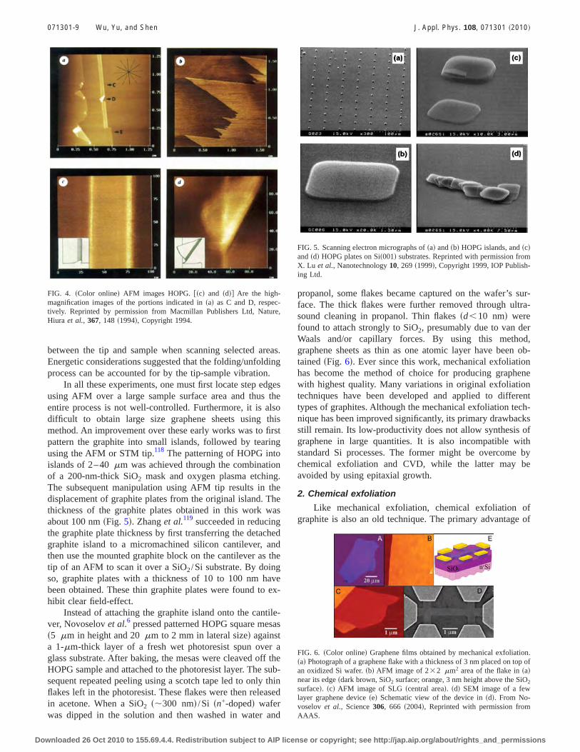
Due to the weak bonding between adjacent graphenesheets in graphite, graphene sheets of different thicknessescan be readily obtained through mechanical exfoliation, orpeeling off, of different types of graphitic materials, includ-ing Kish graphite �single crystal graphite flakes�, highly or-dered pyrolytic graphite �HOPG�, and natural graphite, etc.Mechanical exfoliation of graphite may happen naturally inmany processes such as simply rubbing graphite against aforeign substance, just as writing using a pencil. However,the most recent work with a clearly defined purpose perhapsoriginates from peeling and manipulation of graphene sheetsusing atomic force microscopy �AFM� or STM tips.113–118
Hiura et al.113 and Ebbesen and Himura114 observed foldingand tearing of graphitic sheets which formed spontaneouslyduring scanning due to the friction between the tip andHOPG surface �Fig. 4�. It was found that the folding andtearing of graphitic sheets follow well-defined patterns dueto the formation of sp3-like line defects in the sp2 graphiticnetwork, occurring preferentially along the symmetry axes ofgraphite. The curved portion is accompanied with ripples, inorder to release the strain and stabilize the electronic struc-ture in the bent region. The possibility of creating varioustypes of 3D graphene structures through folding and re-folding of graphene sheets in different ways has beendiscussed.114 Instead of forming graphene sheets spontane-ously during tip scanning on HOPG, Roy et al.116,117 hastried to fold and unfold the graphene sheets in a more con-trollable way through modulating the distance or bias voltage
071301-8 Wu, Yu, and Shen J. Appl. Phys. 108, 071301 �2010�
Downloaded 26 Oct 2010 to 155.69.4.4. Redistribution subject to AIP license or copyright; see http://jap.aip.org/about/rights_and_permissions
between the tip and sample when scanning selected areas.Energetic considerations suggested that the folding/unfoldingprocess can be accounted for by the tip-sample vibration.
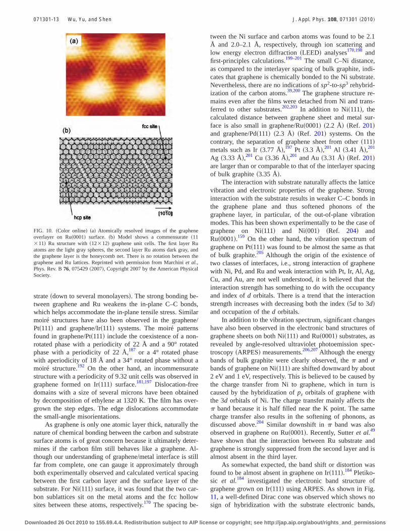
In all these experiments, one must first locate step edgesusing AFM over a large sample surface area and thus theentire process is not well-controlled. Furthermore, it is alsodifficult to obtain large size graphene sheets using thismethod. An improvement over these early works was to firstpattern the graphite into small islands, followed by tearingusing the AFM or STM tip.118 The patterning of HOPG intoislands of 2–40 �m was achieved through the combinationof a 200-nm-thick SiO2 mask and oxygen plasma etching.The subsequent manipulation using AFM tip results in thedisplacement of graphite plates from the original island. Thethickness of the graphite plates obtained in this work wasabout 100 nm �Fig. 5�. Zhang et al.119 succeeded in reducingthe graphite plate thickness by first transferring the detachedgraphite island to a micromachined silicon cantilever, andthen use the mounted graphite block on the cantilever as thetip of an AFM to scan it over a SiO2 /Si substrate. By doingso, graphite plates with a thickness of 10 to 100 nm havebeen obtained. These thin graphite plates were found to ex-hibit clear field-effect.
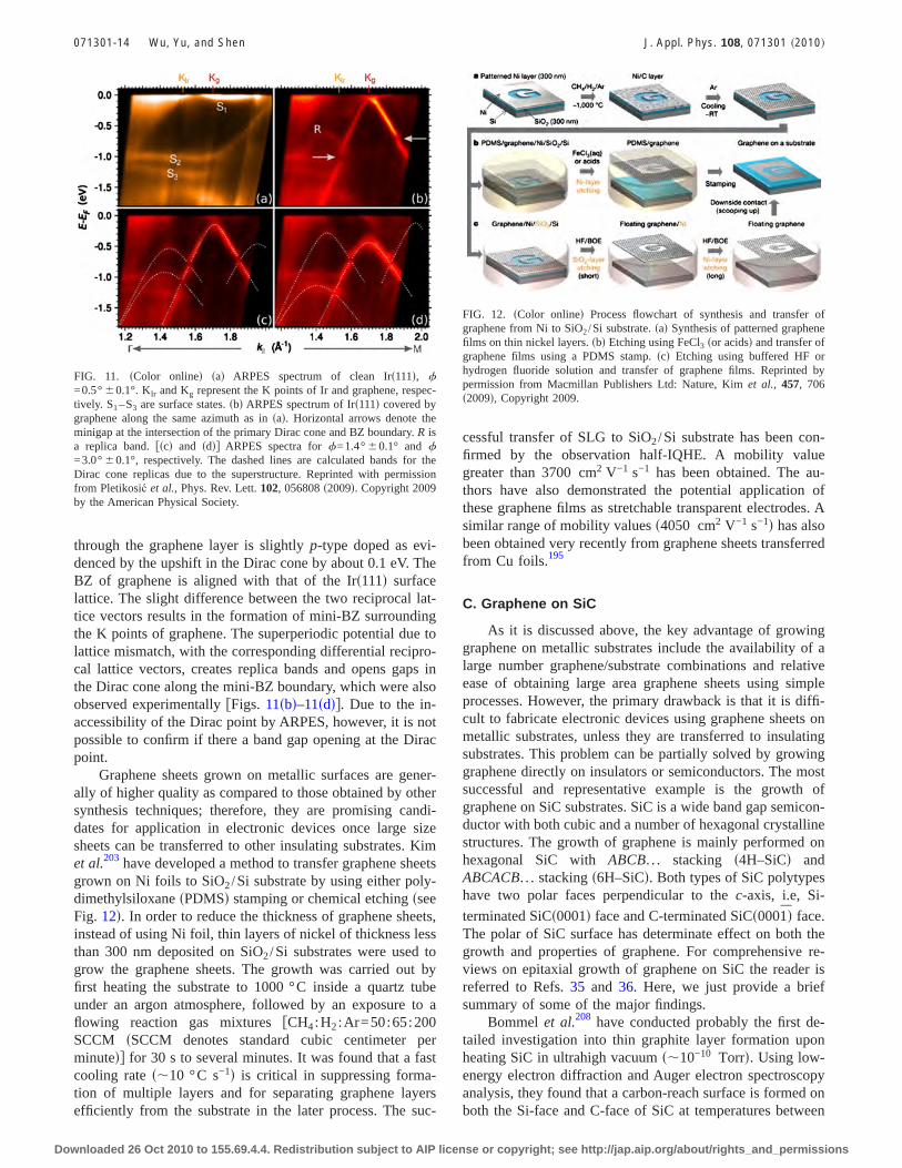
Instead of attaching the graphite island onto the cantile-ver, Novoselov et al.6 pressed patterned HOPG square mesas�5 �m in height and 20 �m to 2 mm in lateral size� againsta 1-�m-thick layer of a fresh wet photoresist spun over aglass substrate. After baking, the mesas were cleaved off theHOPG sample and attached to the photoresist layer. The sub-sequent repeated peeling using a scotch tape led to only thinflakes left in the photoresist. These flakes were then releasedin acetone. When a SiO2 ��300 nm� /Si �n+-doped� waferwas dipped in the solution and then washed in water and
propanol, some flakes became captured on the wafer’s sur-face. The thick flakes were further removed through ultra-sound cleaning in propanol. Thin flakes �d�10 nm� werefound to attach strongly to SiO2, presumably due to van derWaals and/or capillary forces. By using this method,graphene sheets as thin as one atomic layer have been ob-tained �Fig. 6�. Ever since this work, mechanical exfoliationhas become the method of choice for producing graphenewith highest quality. Many variations in original exfoliationtechniques have been developed and applied to differenttypes of graphites. Although the mechanical exfoliation tech-nique has been improved significantly, its primary drawbacksstill remain. Its low-productivity does not allow synthesis ofgraphene in large quantities. It is also incompatible withstandard Si processes. The former might be overcome bychemical exfoliation and CVD, while the latter may beavoided by using epitaxial growth.
2. Chemical exfoliation
Like mechanical exfoliation, chemical exfoliation ofgraphite is also an old technique. The primary advantage of
FIG. 4. �Color online� AFM images HOPG. ��c� and �d�� Are the high-magnification images of the portions indicated in �a� as C and D, respec-tively. Reprinted by permission from Macmillan Publishers Ltd, Nature,Hiura et al., 367, 148 �1994�, Copyright 1994.
FIG. 5. Scanning electron micrographs of �a� and �b� HOPG islands, and �c�and �d� HOPG plates on Si�001� substrates. Reprinted with permission fromX. Lu et al., Nanotechnology 10, 269 �1999�, Copyright 1999, IOP Publish-ing Ltd.
FIG. 6. �Color online� Graphene films obtained by mechanical exfoliation.�a� Photograph of a graphene flake with a thickness of 3 nm placed on top ofan oxidized Si wafer. �b� AFM image of 2 2 �m2 area of the flake in �a�near its edge �dark brown, SiO2 surface; orange, 3 nm height above the SiO2
surface�. �c� AFM image of SLG �central area�. �d� SEM image of a fewlayer graphene device �e� Schematic view of the device in �d�. From No-voselov et al., Science 306, 666 �2004�, Reprinted with permission fromAAAS.
071301-9 Wu, Yu, and Shen J. Appl. Phys. 108, 071301 �2010�
Downloaded 26 Oct 2010 to 155.69.4.4. Redistribution subject to AIP license or copyright; see http://jap.aip.org/about/rights_and_permissions
chemical exfoliation over the mechanical approach lies in itshigh-yield and scalability. The chemical exfoliation is gener-ally accomplished in two process steps. The first step is toenlarge the interlayer spacing between graphene sheets byforming graphite intercalated compounds �GICs�.120,121 TheGICs can be formed in many different forms, depending onthe types of the intercalants,121 although not all of them aresuitable for the subsequent exfoliation process. One of thepopular methods to form GICs for exfoliation purpose is tosoak graphite for an extended period of time in mixtures ofsulfuric and nitric acid.122,123 After an appropriate duration ofsoaking, the acid molecules penetrate into the graphite, form-ing alternating layers of graphite and intercalant. The thick-ness of the graphite layers decreases with time, with a pos-sibility down to a few layers, though the yield of obtainingfew layer graphene sheets is typically quite low. After theintercalation, the second step is to exfoliate the thin graphitesheets via rapid evaporation of the intercalants at elevatedtemperature. The extent of exfoliation can be further en-hanced by subjecting the thermal annealed GICs to treat-ments like ball milling and ultrasonication.123–125 Althoughthis technique is simple, the graphite nanoplatelets obtainedvia this method usually exhibit thicknesses ranging from afew to a few hundreds of layers.123 In order to obtain SLGsheets, the intercalation and exfoliation processes have to berepeated by using different intercalating and exfoliatingchemistry and processes.126,127 Alternatively, one can alsooxidize the graphite completely to form GOs.128,129 The GOscan be subsequently exfoliated to form very thin GO sheetsusing different techniques.130 A chemical, thermal, or elec-trochemical reduction process is then followed to convert theGOs into graphene sheets.131–133 Some typical experimentsare described below.
Aiming at obtaining SLG sheets, Horiuchi and co-workers have developed a two-step process to obtain, whatthey called, carbon nanofilms.134,135 The first step was to oxi-dize the graphite using the Hummer’s method, in which natu-ral graphite particles were immersed in a mixture of H2SO4,NaNO3, and KMnO4 to obtain GICs �or GOs�. In the nextstep, the GOs were hydrolyzed to introduce the hydroxyl andether groups into the intergraphene layer spaces, after whicheach GO layer became a multiply charged anion with a thick-ness of approximately 0.6 nm. When the excess small ionsfrom the oxidants were removed by a purification process,the GO sheets automatically separated from each other dueto interlayer electrostatic repulsion. The resulting GO layersformed a stable dispersion in water. By using this process,Horiuch et al.134 succeeded in obtaining SLG sheets.
Ruoff and co-workers developed a series of processesinvolving the complete exfoliation of GOs into individualGO sheets followed by their in situ reduction to obtain singlegraphene layers.131,136 The process began with the oxidationof graphite using the Hummers method.129 The GOs arestrongly hydrophilic due to the attachment of epoxide andhydroxyl groups to the basal planes and carbonyl and car-boxyl groups at the edges. This makes GOs readily interca-lated with water molecules. The GOs thus obtained are GICswith both covalently bound oxygen and noncovalently boundwater molecules as the intercalants. Rapid thermal treatment
of the GOs results in rapid evaporation of the water mol-ecules at about 100 °C and thermal pyrolysis of oxygen-containing functional groups 250 °C, which in turn help toexfoliate GOs efficiently into individual functionalizedgraphene sheets. The exfoliated GO sheets were dispersed inwater and reduced to graphene sheets by hydrazine reduc-tion. Although the electrical conductivity of reduced GOsheets was found to be five orders of magnitude better thanthe original GO sheets, it is still ten times lower than that ofpristine graphite powders at about 10% of the bulk density.In fact, the electrical transport of reduced GO sheets wasfound to be dominated by hopping.137 This indicates that thereduced graphene sheets likely consist of highly conductinggraphene islands cross-linked by nonconductive regions. Ra-man spectroscopy reveals that the reduced GO sheets arehighly disordered.131,137–139 Figure 7 shows the typical Ra-man spectra of pristine graphite, GO and reduced GO.131 TheRaman spectrum of the pristine graphite displays the well-established G peak as the only feature at 1581 cm−1. The Gpeak is broadened and shifted to 1594 cm−1 in GO. In addi-tion, a strong D band appears at 1363 cm−1, indicating thereduction in size of the in-plane sp2 domains or introductionof disorders during the oxidation process. The Raman spec-trum of the reduced GO is also dominated by the G and Dbands �at 1584 cm−1 and 1352 cm−1, respectively�. The D/G
FIG. 7. �Color online� Raman spectra of pristine graphite �top�, GO�middle�, and the reduced GO �bottom�. Reprinted from Stankovich et al.,Carbon 45, 1558 �2007�, Copyright 2007, with permission from Elsevier.
071301-10 Wu, Yu, and Shen J. Appl. Phys. 108, 071301 �2010�
Downloaded 26 Oct 2010 to 155.69.4.4. Redistribution subject to AIP license or copyright; see http://jap.aip.org/about/rights_and_permissions
intensity ratio increases as compared to that in GO. Thischange suggests a further decrease in the average size of thesp2 domains and increase in defect density or degree of dis-order upon reduction in the GO.
The proposed structures of GO and reduced GO havebeen confirmed recently by Mkhoyan et al.140 using compo-sition sensitive annular dark-field imaging of single andmultilayer GO sheets and electron energy-loss spectroscopyfor measuring the fine structure of C and O K-edges in aSTEM. The results revealed that the GO sheets exhibit anaverage roughness of 0.6 nm and the structure is predomi-nantly amorphous due to distortions of sp2 bonds into sp3
C–O bonds. These works suggest that, in addition to theremoval of oxygen, restoration of the sp2 bonds is necessaryif high mobilities are to be achieved in reduced graphenesheets from GOs. The reduced GOs may find applications inareas which high mobility is not so critical such as transpar-ent conductive thin films141,142 or composite materials.143–145
According to Boukhvalov and Katsnelson and the referencestherein,146–150 the experimentally obtained chemical compo-sition of GO varies in a large range, from C8H2.54O3.91
�Ref. 147� to C8H4.61O6.70,147 C8H1.20–1.60O3.12–3.92,
148
C8– �OH�1.38–1.64O0.63–0.79,149 and C12HO2 to C15H3O4.
150
Based on density functional calculations, Boukhvalov andKatsnelson146 demonstrated that it is difficult to obtain puregraphene through reduction in GO.
Regardless of the types of applications, another commonchallenge of using chemically derived graphene sheets ishow to prevent agglomeration after the reduction from GOs.In this aspect, a few methods have been developed to createcolloidal suspensions of graphene sheets. All these methodsare based on controlled charging of the graphene sheets dur-ing or after the reduction process, including reduction inGOs under basic conditions,151 hydrazine reduction in KOH-modified graphene oxides,152 or introducing sulfonic acidgroups in partially reduced graphene oxides.153
In order to reduce the disorder and defects, several non-oxidation and reduction based methods have been reported.Viculis et al.126 reported the synthesis of graphite nanoplate-lets with thicknesses down to 2–10 nm by using acid-intercalated graphite �Cornerstone, Inc., Wilkes-Barre, PA�as the starting material, reintercalating it with the alkali met-als followed by ethanol exfoliation and microwave drying.The reintercalation was performed either by heating graphiteand potassium or cesium at 200 °C, or at room temperatureusing a sodium–potassium alloy. Exfoliation was achievedby the reaction with ethanol. The final process of microwaveradiation helps to dry and results in further separation of thesheets. Figure 8 shows the scanning electron micrographs of�a� starting graphite, �b� after intercalation with potassiumand exfoliation with ethanol, and �c� and �d� graphite nano-platelets after further exfoliation induced by microwave ra-diation. The scale bars in Fig. 8 are 10 �m, 20 �m,1.67 �m, and 273 nm, respectively. Figure 8�d� shows plate-lets with a thickness of 10–15 nm, which corresponds toapproximately 30–40 layers of graphite. Hernandez et al.154
have demonstrated that graphene dispersions with concentra-tions up to 0.01 mg ml−1 can be produced by dispersion andexfoliation of graphite in organic solvents such as
N-methylpyrrolidone, �-butyrolactone, and 1,3-dimethyl-2-imidazolidinone by sonication of graphite powders. The ex-foliation is made possible by using solvents whose surfaceenergy matches that of graphene. The existence of almostdefect-free SLG and bilayer graphene has been confirmed byTEM, electron diffraction, and Raman, and x-ray photoelec-tron spectroscopies.
Li et al.127 successfully obtained GNRs by first heatingcommercial expandable graphites �made by intercalating�350 �m scale graphite flakes with sulfuric acid andnitric acid� at 1000 °C in a forming gas �3%hydrogen in argon� for 1 min and then sonicating theresulting exfolicated material in a 1,2-dichloroethanesolution of poly�mphenylenevinylene-co-2,5-dioctoxy-p-phenylenevinylene� �0.1 mg/ml� to disperse and break up thegraphenes into small graphene sheets and ribbons. The sub-sequent centrifugation process retains the nanoribbons to-gether with small sheets in the supernatant and removesother materials including large graphene pieces and not fullyexfoliated graphite flakes. It was found that only �0.5% ofthe starting material was retained in the supernatant, and ma-jority of the material remained in many layer structures thatwere heavy and removed by centrifugation. Figure 9 showsGNRs down to sub-10-nm width, which have been subse-quently used to fabricate field-effect transistors �FETs� withon-off ratios of about 107 at room temperature. In a recentwork, the same group reported a significant improvement inthe yield by first exfoliating commercial expandable graphite�160–50 N, Grafguard� via heating it to 1000 °C in a form-ing gas for 1 min, then grounding the exfoliated graphite andreintercalating it with oleum, followed by inserting tetrabu-tylammonium hydroxide �TBA, 40% solution in water� intothe oleum-intercalated graphite in N,N-dimethylformamide�DMF�. The sonication of TBA-inserted oleum-intercalatedgraphite in a DMF solution of 1,2-distearoyl-sn-glycero-3-phosphoethanolamine-N-�methoxy�polyethyleneglycol�-
FIG. 8. Scanning electron micrographs of �a� starting graphite, �b� afterintercalation with potassium and exfoliation with ethanol, and �c� and �d�graphite nanoplatelets after further exfoliation induced by microwave radia-tion. The scale bars in Fig. 8�a�–8�d� are 10 mm, 20 mm, 1.67 mm, and273 nm, respectively. These figures are re-arranged from L. M. Viculis et al.,Mater. Chem. 15, 974 �2005�. Reproduced by permission of the Royal So-ciety of Chemistry.
071301-11 Wu, Yu, and Shen J. Appl. Phys. 108, 071301 �2010�
Downloaded 26 Oct 2010 to 155.69.4.4. Redistribution subject to AIP license or copyright; see http://jap.aip.org/about/rights_and_permissions
5000� for 60 min leads to the formation of a homogeneoussuspension. After large pieces of materials were removedusing centrifugation, a large amount of graphene sheets werethen obtained which are suspended in DMF. AFM measure-ments suggest that 90% of the sheets are individual chemi-cally modified graphene. In order to prevent agglomeration,the graphene sheets have been successfully transferred fromDMF to organic solvent 1,2-dichloroethane.
Fabrication of graphene sheets via chemical routes posesboth potential and challenges. Efforts are required for bothgaining an understanding of the intercalation, oxidation, ex-foliation, reduction, fictionalization, and dispersion processesand developing new starting materials and reaction routes.More details can be found in a recent review.40
B. Graphene on metal surface
Due to the low surface energy of the basal plane, SLG orMLG sheets can be readily formed on selected metal sur-faces via either surface segregation of carbon atoms or ther-mal decomposition of carbon-containing molecules.39 In thefirst method, the source of carbon can either be the smallamount of carbon impurities or intentionally introduced car-bon through annealing the metal in CO atmosphere or incontact with graphite. Then, annealing of the carbon-containing metals at higher temperature causes the carbon tosegregate to the surface. Depending on the annealing tem-perature, the segregated carbon can be in the form of MLGsor SLGs deposited on the surface, or further desorbed fromthe surface. The former is formed when the segregated car-bon reaches thermal equilibrium with the metal. In the sec-ond method, the metal surfaces are first covered by carbon-
containing molecules such as ethylene, propene, methane,acetylene, CO, cyclohexane, a-heptane, benzene, and tolueneat room temperature.39 The subsequent annealing at elevatedtemperature causes desorption of hydrogen, leading to theformation of graphene sheets on the metal surface. The an-nealing can also be performed in the presence of these gas-eous molecules. There have already been several comprehen-sive reviews published on this topic.37–39 We will only givean overview by summarizing some of the main characteris-tics of the films grown on metallic substrates.
The metal substrates that have been investigated includebut are not limited to Co�0001�,155 Ru�0001�,156–166
Pt�100�,188–191,194 Pt�110�,189,190 and Cu.195 In many cases,the substrate’s role is twofold, i.e., functioning as both asubstrate and a catalyst. The latter makes the film growthalmost self-limited; therefore, it is relatively easy to obtainthin graphene films on metal surface. The two key factors ofthe metal surfaces that affect the growth of carbon films areelectronic structure �atomic structure� of the surface �atoms�and the lattice constant. The former determines the nature ofinteractions between the carbon � orbital and the substratesurface atoms, while the latter affects the structure of thegraphene layers, in particular, in the single-layer sheet case.The lattice constants of graphene, Ni�111�, Rh�111�,Ru�0001�, Ir�111�, and Pt�111� are 2.46 Å, 2.49 Å, 2.69 Å,2.71 Å, 2.72 Å, and 2.77 Å, respectively, corresponding to alattice mismatch of 1.2%, 8.5%, 9.2%, 9.6%, and 11.2% be-tween graphene and the substrates.39 Unlike the case of epi-taxial growth of a typical semiconductor material on latticemismatched substrate, in which pseudomorphic growth canbe achieved through the introduction of lattice strains under acertain critical thickness, graphene cannot be strained so eas-ily on metal due to the large anisotropy in chemical bondingstrength between the basal plane and vertical direction.Therefore, except for graphene on Ni�111� in which �1 1�structure is formed due to the small lattice mismatch, in mostother cases, graphene supercells are formed on metallic sub-strates.
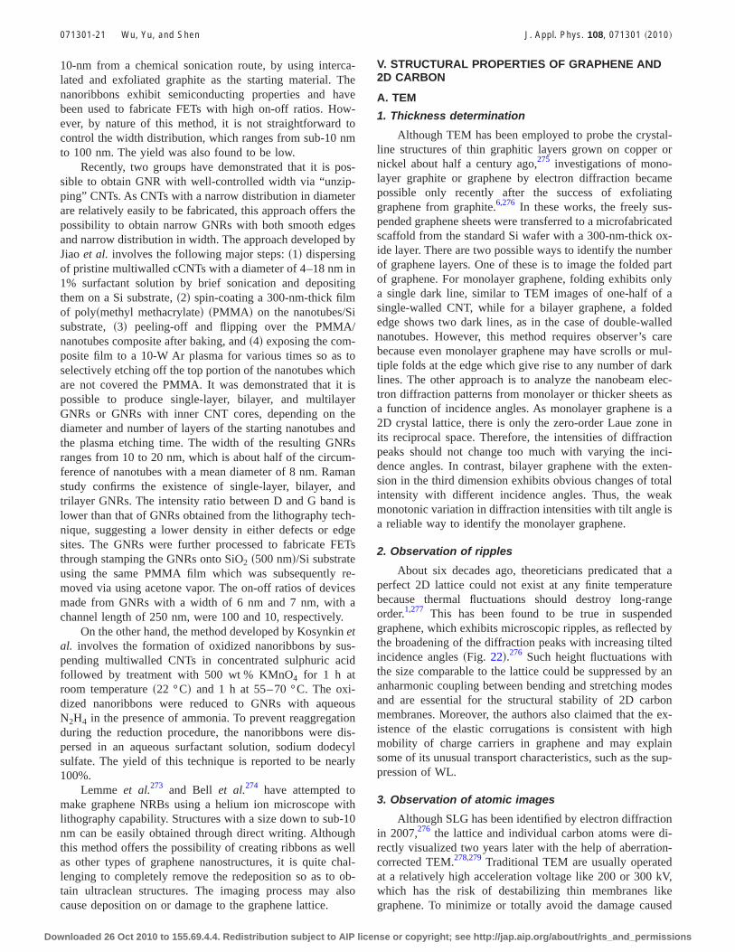
Take Ru�0001� as an example, the typical lattice constantof the supercell obtained from the moiré structure is about 30Å, approximately corresponding to 12 12 graphene on 11 11 Ru�0001� unit cells.157,159–161,166 This has also beenconfirmed by density functional theory �DFT�calculations.196 Figures 10�a� and 10�b� shows the STM im-age of graphene on Ru�0001� and the corresponding latticemodel of the �11 11� superstructure, respectively. The STMimage shows four bright regions and two darker regions ofslightly different brightness. The long-range periodic struc-ture is the moiré structure formed by superposition of 12graphene unit cells and 11 unit cells of the Ru�0001� surface�Fig. 10�b��. The hexagonal lattice can be seen in the moirémaxima. Recently, a superstructure consisting of four moirésubcells was also observed and revealed by surface x-raydiffraction to be 25 25 graphene unit cells on 23 23Ru�0001� unit cells.163 The x-ray diffraction results suggestthat the supercell is formed as the consequence of strongcorrugation of both the graphene and underlying Ru sub-
FIG. 9. �Color online� Chemically derived GNRs down to sub-10-nm width.�a� �Left� Photograph of a polymer PmPV/DCE solution with GNRs stablysuspended in the solution. Right: schematic drawing of a GNR with twounits of a PmPV polymer chain adsorbed on top of the graphene via �stacking. �b� to �f� AFM images of selected GNRs with widths in the 50 nm,30 nm, 20 nm, 10 nm and sub-10-nm regions, respectively. In �b�, leftribbon height �1.0 nm, one layer; middle ribbon height �1.5 nm, twolayers; right ribbon height �1.5 nm, two layers. In �c�, the three GNRs aretwo to three layers thick. In �d�, ribbons are one �right image� to three layers.In �e�, ribbons are two to three layers. In �f�, the heights of the ultranarrowribbons are �1.5 nm, 1.4 nm, and 1.5 nm, respectively. All scale barsindicate 100 nm. From Li et al., Science 319, 1229 �2008�. Reprinted withpermission from AAAS.
071301-12 Wu, Yu, and Shen J. Appl. Phys. 108, 071301 �2010�
Downloaded 26 Oct 2010 to 155.69.4.4. Redistribution subject to AIP license or copyright; see http://jap.aip.org/about/rights_and_permissions
strate �down to several monolayers�. The strong bonding be-tween graphene and Ru weakens the in-plane C–C bonds,which helps accommodate the in-plane tensile stress. Similarmoiré structures have also been observed in the graphene/Pt�111� and graphene/Ir�111� systems. The moiré patternsfound in graphene/Pt�111� include the coexistence of a non-rotated phase with a periodicity of 22 Å and a 90° rotatedphase with a periodicity of 22 Å,187 or a 4° rotated phasewith aperiodicity of 18 Å and a 34° rotated phase without amoiré structure.192 On the other hand, an incommensuratestructure with a periodicity of 9.32 unit cells was observed ingraphene formed on Ir�111� surface.181,197 Dislocation-freedomains with a size of several microns have been obtainedby decomposition of ethylene at 1320 K. The film has over-grown the step edges. The edge dislocations accommodatethe small-angle misorientations.
As graphene is only one atomic layer thick, naturally thenature of chemical bonding between the carbon and substratesurface atoms is of great concern because it ultimately deter-mines if the carbon film still behaves like a graphene. Al-though our understanding of graphene/metal interface is stillfar from complete, one can gauge it approximately throughboth experimentally observed and calculated vertical spacingbetween the first carbon layer and the surface layer of thesubstrate. For Ni�111� surface, it was found that the two car-bon sublattices sit on the metal atoms and the fcc hollowsites between these atoms, respectively.170 The spacing be-
tween the Ni surface and carbon atoms was found to be 2.1Å and 2.0–2.1 Å, respectively, through ion scattering andlow energy electron diffraction �LEED� analyses170,198 andfirst-principles calculations.199–201 The small C–Ni distance,as compared to the interlayer spacing of bulk graphite, indi-cates that graphene is chemically bonded to the Ni substrate.Nevertheless, there are no indications of sp2-to-sp3 rehybrid-ization of the carbon atoms.39,200 The graphene structure re-mains even after the films were detached from Ni and trans-ferred to other substrates.202,203 In addition to Ni�111�, thecalculated distance between graphene sheet and metal sur-face is also small in graphene/Ru�0001� �2.2 Å� �Ref. 201�and graphene/Pd�111� �2.3 Å� �Ref. 201� systems. On thecontrary, the separation of graphene sheet from other �111�metals such as Ir �3.77 Å�,197 Pt �3.3 Å�,201 Al �3.41 Å�,201
Ag �3.33 �,201 Cu �3.36 �,201 and Au �3.31 � �Ref. 201�are larger than or comparable to that of the interlayer spacingof bulk graphite �3.35 �.
The interaction with substrate naturally affects the latticevibration and electronic properties of the graphene. Stronginteraction with the substrate results in weaker C–C bonds inthe graphene plane and thus softened phonons of thegraphene layer, in particular, of the out-of-plane vibrationmodes. This has been shown experimentally to be the case ofgraphene on Ni�111� and Ni�001� �Ref. 204� andRu�0001�.159 On the other hand, the vibration spectrum ofgraphene on Pt�111� was found to be almost the same as thatof bulk graphite.205 Although the origin of the existence oftwo classes of interfaces, i.e., strong interaction of graphenewith Ni, Pd, and Ru and weak interaction with Pt, Ir, Al, Ag,Cu, and Au, are not well understood, it is believed that theinteraction strength has something to do with the occupancyand index of d orbitals. There is a trend that the interactionstrength increases with decreasing both the index �5d to 3d�and occupation of the d orbitals.
In addition to the vibration spectrum, significant changeshave also been observed in the electronic band structures ofgraphene sheets on both Ni�111� and Ru�0001� substrates, asrevealed by angle-resolved ultraviolet photoemission spec-troscopy �ARPES� measurements.206,207 Although the energybands of bulk graphite were clearly observed, the � and �bands of graphene on Ni�111� are shifted downward by about2 eV and 1 eV, respectively. This is believed to be caused bythe charge transfer from Ni to graphene, which in turn iscaused by the hybridization of pz orbitals of graphene withthe 3d orbitals of Ni. The charge transfer mainly affects the� band because it is half filled near the K point. The samecharge transfer also results in the softening of phonons, asdiscussed above.204 Similar downshift in � band was alsoobserved in graphene on Ru�0001�. Recently, Sutter et al.49
have shown that the interaction between Ru substrate andgraphene is strongly suppressed from the second layer and isalmost absent in the third layer.
As somewhat expected, the band shift or distortion wasfound to be almost absent in graphene on Ir�111�.184 Pletiko-sic et al.184 investigated the electronic band structure ofgraphene grown on Ir�111� using ARPES. As shown in Fig.11, a well-defined Dirac cone was observed which shows nosign of hybridization with the substrate electronic bands,
FIG. 10. �Color online� �a� Atomically resolved images of the grapheneoverlayer on Ru�0001� surface. �b� Model shows a commensurate �11 11� Ru structure with �12 12� graphene unit cells. The first layer Ruatoms are the light gray spheres, the second layer Ru atoms dark gray, andthe graphene layer is the honeycomb net. There is no rotation between thegraphene and Ru lattices. Reprinted with permission from Marchini et al.,Phys. Rev. B 76, 075429 �2007�, Copyright 2007 by the American PhysicalSociety.
071301-13 Wu, Yu, and Shen J. Appl. Phys. 108, 071301 �2010�
Downloaded 26 Oct 2010 to 155.69.4.4. Redistribution subject to AIP license or copyright; see http://jap.aip.org/about/rights_and_permissions
through the graphene layer is slightly p-type doped as evi-denced by the upshift in the Dirac cone by about 0.1 eV. TheBZ of graphene is aligned with that of the Ir�111� surfacelattice. The slight difference between the two reciprocal lat-tice vectors results in the formation of mini-BZ surroundingthe K points of graphene. The superperiodic potential due tolattice mismatch, with the corresponding differential recipro-cal lattice vectors, creates replica bands and opens gaps inthe Dirac cone along the mini-BZ boundary, which were alsoobserved experimentally �Figs. 11�b�–11�d��. Due to the in-accessibility of the Dirac point by ARPES, however, it is notpossible to confirm if there a band gap opening at the Diracpoint.
Graphene sheets grown on metallic surfaces are gener-ally of higher quality as compared to those obtained by othersynthesis techniques; therefore, they are promising candi-dates for application in electronic devices once large sizesheets can be transferred to other insulating substrates. Kimet al.203 have developed a method to transfer graphene sheetsgrown on Ni foils to SiO2 /Si substrate by using either poly-dimethylsiloxane �PDMS� stamping or chemical etching �seeFig. 12�. In order to reduce the thickness of graphene sheets,instead of using Ni foil, thin layers of nickel of thickness lessthan 300 nm deposited on SiO2 /Si substrates were used togrow the graphene sheets. The growth was carried out byfirst heating the substrate to 1000 °C inside a quartz tubeunder an argon atmosphere, followed by an exposure to aflowing reaction gas mixtures �CH4:H2:Ar=50:65:200SCCM �SCCM denotes standard cubic centimeter perminute�� for 30 s to several minutes. It was found that a fastcooling rate ��10 °C s−1� is critical in suppressing forma-tion of multiple layers and for separating graphene layersefficiently from the substrate in the later process. The suc-
cessful transfer of SLG to SiO2 /Si substrate has been con-firmed by the observation half-IQHE. A mobility valuegreater than 3700 cm2 V−1 s−1 has been obtained. The au-thors have also demonstrated the potential application ofthese graphene films as stretchable transparent electrodes. Asimilar range of mobility values �4050 cm2 V−1 s−1� has alsobeen obtained very recently from graphene sheets transferredfrom Cu foils.195
C. Graphene on SiC
As it is discussed above, the key advantage of growinggraphene on metallic substrates include the availability of alarge number graphene/substrate combinations and relativeease of obtaining large area graphene sheets using simpleprocesses. However, the primary drawback is that it is diffi-cult to fabricate electronic devices using graphene sheets onmetallic substrates, unless they are transferred to insulatingsubstrates. This problem can be partially solved by growinggraphene directly on insulators or semiconductors. The mostsuccessful and representative example is the growth ofgraphene on SiC substrates. SiC is a wide band gap semicon-ductor with both cubic and a number of hexagonal crystallinestructures. The growth of graphene is mainly performed onhexagonal SiC with ABCB. . . stacking �4H–SiC� andABCACB. . . stacking �6H–SiC�. Both types of SiC polytypeshave two polar faces perpendicular to the c-axis, i.e, Si-
terminated SiC�0001� face and C-terminated SiC�0001� face.The polar of SiC surface has determinate effect on both thegrowth and properties of graphene. For comprehensive re-views on epitaxial growth of graphene on SiC the reader isreferred to Refs. 35 and 36. Here, we just provide a briefsummary of some of the major findings.
Bommel et al.208 have conducted probably the first de-tailed investigation into thin graphite layer formation uponheating SiC in ultrahigh vacuum ��10−10 Torr�. Using low-energy electron diffraction and Auger electron spectroscopyanalysis, they found that a carbon-reach surface is formed onboth the Si-face and C-face of SiC at temperatures between
FIG. 11. �Color online� �a� ARPES spectrum of clean Ir�111�, �=0.5° �0.1°. KIr and Kg represent the K points of Ir and graphene, respec-tively. S1–S3 are surface states. �b� ARPES spectrum of Ir�111� covered bygraphene along the same azimuth as in �a�. Horizontal arrows denote theminigap at the intersection of the primary Dirac cone and BZ boundary. R isa replica band. ��c� and �d�� ARPES spectra for �=1.4° �0.1° and �=3.0° �0.1°, respectively. The dashed lines are calculated bands for theDirac cone replicas due to the superstructure. Reprinted with permissionfrom Pletikosić et al., Phys. Rev. Lett. 102, 056808 �2009�. Copyright 2009by the American Physical Society.
FIG. 12. �Color online� Process flowchart of synthesis and transfer ofgraphene from Ni to SiO2 /Si substrate. �a� Synthesis of patterned graphenefilms on thin nickel layers. �b� Etching using FeCl3 �or acids� and transfer ofgraphene films using a PDMS stamp. �c� Etching using buffered HF orhydrogen fluoride solution and transfer of graphene films. Reprinted bypermission from Macmillan Publishers Ltd: Nature, Kim et al., 457, 706�2009�, Copyright 2009.
071301-14 Wu, Yu, and Shen J. Appl. Phys. 108, 071301 �2010�
Downloaded 26 Oct 2010 to 155.69.4.4. Redistribution subject to AIP license or copyright; see http://jap.aip.org/about/rights_and_permissions
1000 and 1500 °C. The carbon layer is predominantlygraphite after heating at 1500 °C, which has a distinct crys-tallographic relation to the SiC crystal. It was also found thatthe graphite layer is monocrystalline on the Si-face andmostly polycrystalline on the C-face. Subsequent works fur-ther confirmed the difference in graphitization processes be-tween Si-face and C-face,209 and revealed that the thin graph-ite layer on Si-face is epitaxial with its lattice rotated 30°
with respect to SiC�1010� direction210 while that on C-facegenerally exhibits multiple orientational phases.211
Although significant progresses have been made recentlyin this field, in particular, the success in growing single andfew layer graphene sheets on SiC,212,213 understanding of theentire process from surface reconstruction to Si-sublimationand graphitization is still far from complete. A typicalgraphene growth process on Si-face SiC begins with thepreparation of SiC surface. The exact preparation procedurevaries, depending on the original surface condition of thesubstrate that is used. In most cases, a hydrogen etch is em-ployed to remove the scratches and obtain regular atomicstepped surfaces.36,214–217 Heating the substrate to about800–1000 °C in UHV and in the presence of Si flux re-moves the oxide layer and at the same time leads to theformation of a Si-rich �3 3� phase.36,218–220 Starting fromthis �3 3� phase, a series of intermediate phases would ap-pear before a C-rich �6�3 6�3�R30 phase is formed atabout 1100 °C.36,220–224 There are no unified patterns of ap-pearance of the intermediate phases; in addition to tempera-ture, the appearance of a specific surface reconstruction isalso dependent on the quality of the original substrate sur-face, and heating methods, speed, atmosphere, etc. As theC-rich �6�3 6�3�R30 phase serves as the precursor ofgraphene growth, homogeneity of this phase plays a crucialrole in determining the growth and properties of thegraphene layers, which is induced by further heating thesample to 1200–1350 °C.36,222
One of the bottlenecks in growing graphene on Si-faceSiC is the roughening of the substrate accompanied bygraphitization, which significantly limits the domain size ofthe graphene. Regardless of the initial step size of the sub-strate, the average step size after graphene formation ismostly in the range of 20–50 nm.36,222 The large roughnesssuggests that the surface is far from equilibrium during thegraphitization process, preventing it from achieving asmooth morphology. Using in situ low-energy electron mi-croscopy �LEEM�, Tromp and Hannon showed that the phasetransformation temperatures can be varied over a large tem-perature range and the transformation time can be reduced byseveral orders of magnitude, via balancing the rate of Sievaporation and an external flux of Si.221 The ability toachieve quasiequilibrium at higher temperature in the pres-ence of disilane greatly reduce the phase transformation timewhich in turn makes it possible to obtain homogeneous�6�3 6�3�R30 phase with a large domain size. This mayeventually lead to the reduction in final surface roughness ingraphene grown on the Si-face SiC.
Instead of heating SiC in UHV, Emtsev et al.225 haveshown that wafer-size graphene layers can be obtainedthrough ex situ graphitization of Si-terminated SiC�0001� in
an argon atmosphere of about 1 bar. They have compared thesurface morphologies of graphene obtained from two differ-ent routes with that of hydrogen etched substrate. As shownin Fig. 13�a�, the hydrogen etched 6H–SiC�0001� surfaceexhibits a well-defined terrace structure as determined byAFM. For this specific sample, the terrace width is of theorder of 300–700 nm, which are determined by the incidentalmisorientation of the substrate surface with respect to thecrystallographic �0001� plane, and the step height is 1.5 nm,which corresponds to the size of one 6H–SiC unit cell in caxis. However, after the growth of a monolayer of grapheneby vacuum annealing, the original steps are hardly seen inthe AFM image, as shown in Fig. 13�b�. This agrees with thewell-documented facts that the graphene growth is accompa-nied by substantial roughening of the substrate surface.36,222
The LEEM image �Fig. 13�c�� confirms that the so fabricatedgraphene has an inhomogeneous thickness distribution, in-cluding regions coexisting with graphene bilayer islands anduncovered �6�3 6�3� buffer layer. The surface morphologyof graphene improves drastically, obtained by heating theSiC under 900 mbar of argon at 1650 °C, as demonstratedby the AFM image in Fig. 13�d�. Large continuous terracesare formed through step bunching, leading to macroterracesthat are a factor of five to eight times wider than the originalterraces, 50 �m long along the step edges, and have an av-erage height of 8–15 nm. The LEEM images, Figs. 13�e� and13�f�, show that the graphene sheets grown by annealing SiCin the presence of Ar have a remarkable uniform thicknessdistribution. The spatially resolved LEEM I-V spectra �Figs.13�g� and 13�h��, taken along a vertical and a horizontal linein Fig. 13�f�, allow the authors to conclude that except fornarrow stripes at the edges, the large atomically flat macrot-erraces are homogeneously covered with a graphene mono-layer. The narrower and darker regions at the downwardedges of the terraces correspond to bilayer and in some casestrilayer graphene. In the AFM images shown in Fig. 13�i�,these regions appear as small depressions of around 0.5 and1 nm amplitude located at the edge of the macrostep, sug-gesting that the nucleation of new graphene layers starts atstep edges of the substrate surface. The authors attribute theimprovement of surface morphology to significantly higherannealing temperature of 1650 °C, as compared with1280 °C in UHV. A higher temperature growth is attainablebecause the presence of a high pressure of argon leads to areduced Si evaporation rate. The significantly higher growthtemperature in turn results in an enhancement of surface dif-fusion, which ultimately leads to the markedly improved sur-face morphology.
Compared to the bulk number of work on Si-face, thereare much fewer studies on the growth of graphene on C-faceSiC. Unlike Si-face, generally it is more difficult to preparethe surface of C-face SiC in UHV.222 In this context, Hass etal.36,226 have developed a method to prepare C-face 4H–SiCsamples by heating them in a vacuum rf-induction furnace ata pressure of P=3 10−5 Torr. The samples were firstheated to 1200 °C for about 20 min to outgas the furnaceand remove the surface oxide from SiC. After this step thefurnace is quickly ramped to �1420 °C, at which 4–13 lay-
071301-15 Wu, Yu, and Shen J. Appl. Phys. 108, 071301 �2010�
Downloaded 26 Oct 2010 to 155.69.4.4. Redistribution subject to AIP license or copyright; see http://jap.aip.org/about/rights_and_permissions
ers of graphene grow in about 5–8 min.36,227 The quality ofgraphene grown by annealing in rf furnace is exceptionallygood.
The separation between the first graphene layer and theSiC surface is found to be only 1.62 Å, implying that there isa very strong interaction between the first graphene layer andthe substrate.227 This strongly bonded layer serves as a bufferto reduce the effect of the substrate exerting on the secondlayer and above, leading to an rms roughness of �0.05 Å.Hass et al.48,228 have found that, unlike Si-face films, theC-face epitaxial graphene can grow in following three mainrotated phases: layers rotated 30° �R30� or �2.20° �R2��with respect to the SiC �1010� direction. Surface x-ray dif-fraction and STM showed that these three rotated phases areinterleaved in the film, causing a high density of stackingfault boundaries between the R30 and R2� layer. This newstacking sequence preserves the electronic symmetry of an
isolated graphene sheet in C-face grown films,171 as con-firmed by the observation of high mobility and other charac-teristics of SLG in MLG sheets.69,227 As one of the example,Fig. 14 shows the recently reported LL spectrum of SLGfrom MLG sheets grown on the carbon-face of 4H–SiC
�0001� substrate. The unique features of LLs in graphene�see Sec. II A� are clearly demonstrated in Fig. 14. As shownin the inset of Fig. 14�a�, the coupling between the topmostlayer and the remaining layers is essentially zero. Thisunique feature makes C-face grown graphene more promis-ing for electronics applications.
D. Synthesis of free-standing 2D carbon
In addition to expitaxial growth, 2D carbon can also begrown in a free-standing form, just like 0D and 1D carbonnanostructures. In fact, 2D carbon often coexists with 0D and
FIG. 13. �Color online� �a� AFM image of H-etched 6H–SiC�0001� surface; �b� AFM image of graphene on 6H–SiC�0001� with a nominal thickness of onemonolayer formed by annealing in UHV at a temperature of about 1280 °C; �c� LEEM image of a UHV-grown graphene film with a nominal thickness of 1.2monolayer; light, medium, and dark gray correspond to a local thickness of zero monolayer, one monolayer, and two monolayer, respectively; �d� AFM imageof graphene with a nominal thickness of 1.2 monolayer formed by annealing in Ar�p=900 mbar, T=1650 °C�; �e� LEEM image of a sample equivalent tothat of �d�; �f� Close-up of the image shown in �e�; �g� and �h� electron reflectivity spectra taken at the positions indicated by the lines in �f�; �i� close-up AFMimages of the film shown in �d�. Reprinted by permission from Macmillan Publishers Ltd: Nature, Emtsev et al., 8, 203 �2009�, Copyright 2009.
071301-16 Wu, Yu, and Shen J. Appl. Phys. 108, 071301 �2010�
Downloaded 26 Oct 2010 to 155.69.4.4. Redistribution subject to AIP license or copyright; see http://jap.aip.org/about/rights_and_permissions
1D structures during the preparation of the latter using laserablation and arc discharge.45,228 The ratio of 2D carbon overthe 0D or 1D structure depends strongly on the experimentalcondition. A general trend is that the lower the growth tem-perature the higher the yield of 2D carbon. By optimizing thecurrent and hydrogen pressure in dc arc discharge, Ando etal.112 found a large amount of petal-like graphite sheets out-side the flame region of arc discharge as well as on thegraphite wall surrounding the anode and cathode. Thesenanosheets are highly curved and interlaced with one an-other, forming spongelike structures.
Compared to laser ablation and arc discharge, the CVDoffers a much larger process window for controlling theshape and dimension of carbon nanostructures. In particular,it allows for the growth of 2D carbon nanostructures on for-eign substrates, which are important for many applications.Wu et al.41,42,229,230 reported on the growth of verticallyaligned 2D carbon nanostructures on various types of sub-strate, dubbed CNWs, using MWPECVD. In addition toMWPECVD,46,231–237 similar types of 2D carbon nanostruc-tures have also been successfully grown using other tech-niques such as rf-PECVD �Refs. 43, 44, and 238–245� andhot filament CVD �HFCVD�.246–249 In what follows, we givean overview of CNWs grown by MWPECVD.
As shown schematically in Fig. 15, the MWPECVD sys-tem used by Wu et al.41,42,229,230 is equipped with a 500 Wmicrowave source and a traverse rectangular cavity to couplethe microwave to a quartz tube for generating the plasma.Inside the quartz tube are two parallel plate electrodes placed2 cm away from each other in the longitudinal direction ofthe tube, for applying a dc bias during the growth. The gasesused were mixtures of CH4 and H2. In this simple setup, asthere is no independent substrate heater, the substrate tem-perature is in the range of 650–700 °C, determined by thepower of the microwave source. Apart from the temperature,other important parameters which affect the growth of car-bon nanostructures are H2 /CH4 flow rate ratio and electricalfield. The latter consist of both a global dc field, variable bythe applied dc bias, and localized ac field due to the plasmaitself.
Wu et al.41 have carried out a series of experiments togrow the CNWs using different H2 /CH4 flow rate ratios. Itwas found that there was hardly any growth with a H2 /CH4
flow rate ratio �50, for a duration of �5 min. Figure 16shows the morphology of the carbon nanostructures grownon Au ��20 nm� coated Si substrates with a fixed gas pres-sure of 1 Torr but different H2 /CH4 flow rate ratios. Whenthe H2 /CH4 flow rate ratio was reduced to 30, some colum-nar structure of amorphous carbon formed. Further decreasein the gas flow rate ratio led to the formation of a mixture ofcarbon fibers/tubes and 2D nanographite sheets. A pure formof CNWs forms when the gas flow rate ratio is in the rangeof 4–8. Too low a gas flow rate ratio would again lead to theformation of amorphous carbon. An optimum H2 /CH4 flowrate ratio was found in these studies.
Figure 17�a� shows a typical SEM image of the CNWsgrown under optimum conditions.41 The distribution of thenanowalls was found to be remarkably uniform over the
FIG. 14. �Color online� LL spectrum in epitaxial graphene. �a� Tunneling differential conductance spectra vs sample bias of LLs in MLG at B=5 T �blue dot:experimental data; red line: fitting in Voigt line shape at LL peak positions�. Inset shows the LL peak position vs square root of LL index and applied field fromthe peak positions in �a�. Solid lines are fits to a bilayer model with interlayer coupling of zero �red�, 150 meV �black�, and 300 meV �blue�. �b� LL spectrafor various applied magnetic fields from 0 to 6 T. The curves are offset for clarity �tunneling set point, Vb=350 mV, I=400 pA�. �c� LL peak energies forapplied fields of 1 to 8 T, showing a collapse of the data when plotted vs square root of LL index and applied field. The solid line shows a linear fit yieldinga characteristic velocity of c�= �1.128�0.004� 106 ms−1. Inset: the shift in the LL0 peak position as a function of applied field �symbols�. The solid line isa linear fit to the data points. From Miller et al., Science 324, 924 �2009�. Reprinted with permission from AAAS.
FIG. 15. �Color online� Schematic of MWPECVD used in Refs. 41, 42, 229,and 230.
071301-17 Wu, Yu, and Shen J. Appl. Phys. 108, 071301 �2010�
Downloaded 26 Oct 2010 to 155.69.4.4. Redistribution subject to AIP license or copyright; see http://jap.aip.org/about/rights_and_permissions
whole substrate surface area that is typically 1 1 cm2. Fig-ure 17�b� shows some of the nanowalls peeled off from thesubstrate and lie down on top of the nanowall samples. Thenanowalls grow very fast at the first 1–2 min and nearly stopgrowing after they reach a height of about 2 �m. The widthis in the range of 0.1–2 �m; it increases with decreasing thenanowall density. The thickness of the nanowalls is typicallyin the range of one to several nanometers, although sheets asthin as two monolayers were observed by high-resolutiontransmission electron microscope �HRTEM�, as shown inFig. 18.41,250 It is interesting to note that, for some CNWs,the thickness decreases along the growth direction, ap-proaching one monolayer at the top edges. As will be dis-cussed in detail in the later part of this review, Raman spec-troscopy revealed that the CNWs contains highly graphitizeddomains embedded in a disordered 2D carbon host matrix.
Hiramatsu and co-workers investigated the growth ofCNWs using various types of mixtures of fluorocarbon/hydrogen gases, including C2F6 /H2, CH4 /H2, CF4 /H2,CHF3 /H2, and C4F8 /H2, in an rf-PECVD system which con-sists of a parallel-plate rf �13.56 MHz� capacitively coupledplasma chamber and a remote inductively coupled or a sur-face wave microwave �2.45 GHz� excited H2 plasma as aradical source.44,244,251 The use of a separate H2 plasmasource allowed the authors to study quantitatively the role ofhydrogen atom or radicals in the growth of CNWs. The mor-phologies and growth rate of CNWs were found to be depen-dent on both the types of carbon sources and rf power of theremote H2 plasma source.251 Among all the gas mixturesinvestigated, C2F6 /H2 gave the highest growth rate which isattributed to the effective generation of CF3 radicals.244 Onthe other hand, there was no growth of CNWs using eitherthe C4F8 /H2 mixture or any other carbon source gases with-out hydrogen. The main role of the H radicals lies in theremoval of undesirable amorphous phase during the growth,leading to improved surface morphology and crystallinequality of CNWs. This has been confirmed by measuring theCFx /H2 ratio quantitatively and correlating it with the sur-face morphology of as-grown CNWs.244
Chuang et al.232 reported on the MWPECVD growth ofCNWs using a gas mixture of NH3 /C2H2. It was found thatthe nanowalls began to grow when the NH3 /C2H2 flow rateratio falls below 1 and the growth rate increases with furtherdecreasing the NH3 /C2H2 flow rate ratio. The CNWs showmore well-defined graphitic wall structures with the increas-ing ammonia ratio, indicating that the ammonia radicals actas an etchant during the growth of nanowalls, a similar roleplayed by hydrogen in the cases where hydrogen is used asthe source gas.
Compared to MWPECVD and rf-PECVD, HFCVD re-ported to be more suitable for smaller and thus densernanoflakes246 or nanowalls.247 Using C2H2 �3%–15%� /H2
mixture as the source gases, Shang et al.246 demonstratedthat the carbon nanoflakes deposited on Si�100� substrate at400–600 °C have a thickness of less than about 10–20 nmand a lateral size of 300–600 nm. In this temperature range,the size and density of the nanoflakes decreases and in-creases, respectively, as the temperature increases. When thesubstrate temperature was increased to 700 °C, the thicknessand lateral size of the carbon flakes decreases to about 5 nmand 80 nm, respectively, leading to the formation of a verydense film. Dikonimos et al.247 investigated the effect of a dc
FIG. 17. SEM images of CNWs grown at a H2 /CH4 flow rate ratio of 4.Scale bars: �a� 100 nm and �b� 1 �m. �a� Was taken at a tilt angle of 25°.Y. H. Wu et al., J. Mater. Chem. 14, 469 �2004�. Reproduced by permissionof the Royal Society of Chemistry.
FIG. 18. HRTEM images of CNWs grown at a H2 /CH4 flow rate ratio of 4.Reprinted with permission from Yang, Ph.D. thesis, National University ofSingapore, 2004.
FIG. 16. SEM images of carbon nanostructures grown at different H2 /CH4
flow rate ratios. �a� 30, �b� 15, �c� 10, �d� 6, �e� 4, �f� 1. Scale bars: �a�, �b�,�d�, and �f� 1 �m, �c� and �e� 100 nm. Y. H. Wu et al., J. Mater. Chem. 14,469 �2004�. Reproduced by permission of the Royal Society of Chemistry.
071301-18 Wu, Yu, and Shen J. Appl. Phys. 108, 071301 �2010�
Downloaded 26 Oct 2010 to 155.69.4.4. Redistribution subject to AIP license or copyright; see http://jap.aip.org/about/rights_and_permissions
plasma on the HFCVD growth of nanowalls using CH4 /Heas the gas mixture. Both the thickness and lateral size ini-tially increase with increasing the plasma current which sub-sequently saturate at a total plasma current of 100 mA in thatspecific setup. CNWs with a maximum lateral size rangingfrom 10 to 200 nm and thickness lower than 5 nm, have beengrown on Si substrates. Both the lateral size and density aremuch higher than those of nanowalls grown by rf-PECVD orMWPECVD. Well-aligned CNWs were also successfullysynthesized by an electron beam excited PECVD using amixture of CH4 and H2 at a total pressure of 2–4 Pa and atemperature of 570 °C.252
The CNWs or nanosheets can be grown on any type ofsubstrates without catalyst as long as the substrate can sus-tain the growth temperature which is typically below800 °C.41,43 Unlike the CNT case, the growth mechanism of2D carbon by CVD is still not well understood. Zhu et al.253
proposed a model for the growth of 2D carbon nanosheetsusing rf-PECVD. In their experiments, the nanosheets weredeposited on a variety of substrates in an inductively coupledplasma from a gas mixture of CH4�5%–100%� /H2, at a totalgas pressure of 20–400 mTorr, substrate temperature of600–950 °C, and rf power of 400–1200 W. According tothis model, the nanosheet initially grows parallel to the sub-strate up to a thickness of 1–15 nm before the onset of ver-tical growth. The formation of parallel layer has been con-firmed by surface x-ray scattering measurements.254 Thelatter is presumably caused by the building up of upwardcurling force at the grain boundaries of nanographite do-mains. Once the nanosheet is oriented in the vertical direc-tion, it grows much faster in the direction parallel to thesheet due to the very high surface mobility of incoming Catoms or CHx radicals and polarization of the graphitic layersinduced by the local electric field in the sheath layer �Fig.19�. The fast diffusion of carbon-bearing species and etchingby hydrogen radicals strongly suppress the growth in thick-ness direction. Once they reach the edges, however, thecarbon-bearing species will form bonds with edge atoms,leading to the growth in height direction. The free-standing2D carbon formed by various types of plasma processes con-tains a high density of defects due to the bombardment by
high energy electrons, ions and radicals. This has been re-vealed by Raman spectroscopy42,240,255 and TEM.256
Wu et al.41,230 have conducted a series of experiments toinvestigate the effect of lateral field on the growth of CNWsby making use of strong electrical field surrounding metallicnanoparticles on an insulating substrate or sharp features cre-ated by anisotropic etch of Si. In the former case, the strongelectrical field is associated with the excitation of surfaceplasmon, while the latter is due to the large surface curva-ture. The surface plasmon was created by exciting the Aunanoparticles on sapphire substrate using the photon emis-sions from the plasma. The Au particles in turn were ob-tained through annealing the Au films in a hydrogen plasmaenvironment.230 It was found that the influence of the surfaceplasmon to the growth of CNWs was a rather drastic one.Figure 20 summarizes the unique CNW patterns that havebeen observed due to the presence of surface plasmon. Thecircular region consists of an outer ring with denser nanow-alls and a flower-like nanowall structure at the center. Thelatter consists of one to several poles and the number ofpoles increases with the density of the nanowalls surround-ing the circular region, so is the size of the entire region �seeFigs. 20�a�–20�h��. However, the occupation ratio of theouter ring in the whole circular region decreases when thenumber of poles increases. Figure 20�i� shows an enlargedview of the boundary between the circular region and theregion surrounding it. It shows clearly that the nanowallsorient randomly outside the circular region, while they alignwell along the circumference direction in the rim region andchange the direction by almost 90º when they move furtherto the central region. This large change in wall orientationwithin a very localized region could hardly be possible with-out the existence of strongly localized electric fields inducedby the surface plasmon. The patterns shown in panels �a�–�h�resemble well the electric field distribution of multiple polesurface plasmon �SP� predicted by Mie’s theory with thenumber of poles increasing from �a�–�h�.257 The size of thepattern increases with the number of poles. It is about 8 �mfor the dipole pattern shown in panel �a� and 20 �m for themultiple pole patterns shown in �g� and �h�. Assume that the
FIG. 19. Schematic of the growth model of carbon nanosheets. E� : electricfield near a substrate surface; CHx: carbon-bearing growth species imping-ing from gas phase; Cg: growth species diffuse along carbon nanosheetsurface; H: atomic hydrogen impinging from gas phase; CHy: defects re-moved from carbon nanosheet by atomic hydrogen etching effects. Re-printed from Zhu et al., Carbon 45, 2229 �2007�, Copyright 2007, withpermission from Elsevier.
FIG. 20. SEM images of CNW patterns formed by the electrical field ofsurface plasmons with different number of poles. �i� is the enlarged image ofportion �a� in �h�. Scale bars: 1 �m. Adapted with permission from Wu etal., Nano. Lett. 2, 355 �2002�. Copyright 2002, American Chemical Society.
071301-19 Wu, Yu, and Shen J. Appl. Phys. 108, 071301 �2010�
Downloaded 26 Oct 2010 to 155.69.4.4. Redistribution subject to AIP license or copyright; see http://jap.aip.org/about/rights_and_permissions
surface plasmon emission travels at the same speed of lightin vacuum, it gives a lifetime of about 25 fs and 70 fs, re-spectively. These values agree well with the reported lifetimefor surface plasmons in literature. In addition to gaining aninsight into the growth mechanism of CNWs, this work hasalso successfully “fingerprint” the electric field of surfaceplasmon at nanometer scale accuracy. This is a remarkableresult because it is the only technique reported so far whichcan detect the electrical field instead of the intensity of thesurface plasmons. Similar type of plasmon-based techniquehas been employed elsewhere to assist the growth and fabri-cation of various types of nanostructures.258–260
The free-standing 2D carbon nanostructures are particu-larly suitable for field emission applications.41,43,239,261–265
Wu et al.41 carried out a series of experiments to investigatethe field emission characteristics of the CNWs grown on Cusubstrates. The turn-on electrical field was found to be in therange of 1–1.5 V /�m at an emission current density of10 �A /cm2 and at room temperature. The small thresholdelectrical field is attributed to the sharp edges and goodalignment of the nanowalls on the substrates grown by MW-PECVD. Figure 21�a� shows the emission current densitiesas a function of the applied electric field for one of suchsamples obtained at temperatures of 20 °C, 200 °C, 300 °C,and 400 °C, respectively, and at an anode–cathode distanceof 50 �m. The experiments were carried out at 20 °C first,and then were repeated at different temperatures after thesubstrate was heated up using a resistive heater and stabi-lized at each temperature setting point. The turn-on electricfield decreased to 0.26 V /�m, 0.2 V /�m, and 0.16 V /�mwith the temperature increasing to 200 °C, 300 °C, and400 °C, respectively. Figure 21�b� shows the ln�I /V2� versus1 /V, or Fowler–Nordheim �FN� plot, where V is the appliedvoltage between the cathode and anode. It was observed that
FN plot is linear at 300 and 400 °C but deviates from thelinear relationship at low temperature. It was argued thatthere exist two energy barriers with different height at lowertemperatures, which could be caused by the absorbates onthe nanowall surfaces. The absorbates in this case are mostlikely hydrogen because the nanowalls were grown using amixture gas of CH4 and H2. Araidai et al.266 investigatedfield emission from graphitic ribbons by first-principles cal-culations based on time-dependent DFT. It was found thatthe field emission current from graphitic ribbons dependsstrongly on the hydrogen termination and the direction of theapplied electric field. Recently, Elias et al.267 demonstratedthat the electronic properties of SLG can be readily modifiedthrough a reversible hydrogenation process. The absorbedhydrogen can be completed removed through thermal an-nealing at 300 °C. Luo et al.268 have conducted a more de-tailed study about the hydrogen desorption processes throughmonitoring the D band to G band intensity ratio of the Ra-man spectrum. The results show that the dehydrogenationoccurs in two processes with different activation energies.The dehydrogenation occurs rapidly below 200 °C, beyondwhich it processes slowly and is completed at 300 °C, agree-ing well with the trend observed in field emission.
Compared to 2D carbon grown on different types of sub-strate, the largest advantage of free-standing carbon is thatthe effect of substrate on the electrical transport properties isalmost negligible. Of course, at the same time, this is also thedrawback because it is difficult to form electrodes for elec-trical transport measurements. Wu and co-workers have stud-ied the electrical transport properties of CNWs using boththe top41 and bottom electrodes.269 The former allows theauthors to study the transport properties across self-assembled 2D carbon networks, which exhibits interestingoscillations in MR. The latter makes it possible to study thetransport of a single piece of free-standing nanosheets.Takeuchi et al.173 have attempted to control the conductivityof CNWs through nitrogen doping. If both p and n-type con-ductivity can be obtained through doping, it is possible toform nanometer scale p-n junctions of 2D carbon on wafer-level. The nanowalls can also be used as templates to formother types of nanostructures or junctions.270
E. Fabrication of GNRs
The exceptionally high mobility makes graphene veryappealing for electronics applications.32,108 However, the ma-jor obstacle to applying graphene in electronics, especiallyFETs is its lack of band gap. Although a sizable gap can beopened in graphene through making it into narrowribbons,70,74,77 as discussed in Sec. II C, it is quite challeng-ing experimentally to make nanoribbons with sharp edges.Top-down techniques such as the combination of e-beam li-thography and etching are certainly the natural choices forfabricating GNRs. However, the ribbons produced by thisapproach tend to have rough edges and the width attained sofar is insufficient to have a sizable gap.271,272 The roughedges make it difficult to differentiate real gaps from thetransport gap. As it is discussed in Sec. IV A 2, Li et al.127
have successfully produced GNRs with a width of sub-
FIG. 21. �a� Emission current density as a function of the electrical field atdifferent temperatures for CNWs and �b� the corresponding FN plots of thecurves in �a�. The inset of �a� shows the sample configuration for fieldemission measurement. Y. H. Wu et al., J. Mater. Chem. 14, 469 �2004�.Reproduced by permission of the Royal Society of Chemistry.
071301-20 Wu, Yu, and Shen J. Appl. Phys. 108, 071301 �2010�
Downloaded 26 Oct 2010 to 155.69.4.4. Redistribution subject to AIP license or copyright; see http://jap.aip.org/about/rights_and_permissions
10-nm from a chemical sonication route, by using interca-lated and exfoliated graphite as the starting material. Thenanoribbons exhibit semiconducting properties and havebeen used to fabricate FETs with high on-off ratios. How-ever, by nature of this method, it is not straightforward tocontrol the width distribution, which ranges from sub-10 nmto 100 nm. The yield was also found to be low.
Recently, two groups have demonstrated that it is pos-sible to obtain GNR with well-controlled width via “unzip-ping” CNTs. As CNTs with a narrow distribution in diameterare relatively easily to be fabricated, this approach offers thepossibility to obtain narrow GNRs with both smooth edgesand narrow distribution in width. The approach developed byJiao et al. involves the following major steps: �1� dispersingof pristine multiwalled cCNTs with a diameter of 4–18 nm in1% surfactant solution by brief sonication and depositingthem on a Si substrate, �2� spin-coating a 300-nm-thick filmof poly�methyl methacrylate� �PMMA� on the nanotubes/Sisubstrate, �3� peeling-off and flipping over the PMMA/nanotubes composite after baking, and �4� exposing the com-posite film to a 10-W Ar plasma for various times so as toselectively etching off the top portion of the nanotubes whichare not covered the PMMA. It was demonstrated that it ispossible to produce single-layer, bilayer, and multilayerGNRs or GNRs with inner CNT cores, depending on thediameter and number of layers of the starting nanotubes andthe plasma etching time. The width of the resulting GNRsranges from 10 to 20 nm, which is about half of the circum-ference of nanotubes with a mean diameter of 8 nm. Ramanstudy confirms the existence of single-layer, bilayer, andtrilayer GNRs. The intensity ratio between D and G band islower than that of GNRs obtained from the lithography tech-nique, suggesting a lower density in either defects or edgesites. The GNRs were further processed to fabricate FETsthrough stamping the GNRs onto SiO2 �500 nm�/Si substrateusing the same PMMA film which was subsequently re-moved via using acetone vapor. The on-off ratios of devicesmade from GNRs with a width of 6 nm and 7 nm, with achannel length of 250 nm, were 100 and 10, respectively.
On the other hand, the method developed by Kosynkin etal. involves the formation of oxidized nanoribbons by sus-pending multiwalled CNTs in concentrated sulphuric acidfollowed by treatment with 500 wt % KMnO4 for 1 h atroom temperature �22 °C� and 1 h at 55–70 °C. The oxi-dized nanoribbons were reduced to GNRs with aqueousN2H4 in the presence of ammonia. To prevent reaggregationduring the reduction procedure, the nanoribbons were dis-persed in an aqueous surfactant solution, sodium dodecylsulfate. The yield of this technique is reported to be nearly100%.
Lemme et al.273 and Bell et al.274 have attempted tomake graphene NRBs using a helium ion microscope withlithography capability. Structures with a size down to sub-10nm can be easily obtained through direct writing. Althoughthis method offers the possibility of creating ribbons as wellas other types of graphene nanostructures, it is quite chal-lenging to completely remove the redeposition so as to ob-tain ultraclean structures. The imaging process may alsocause deposition on or damage to the graphene lattice.
V. STRUCTURAL PROPERTIES OF GRAPHENE AND2D CARBON
A. TEM
1. Thickness determination
Although TEM has been employed to probe the crystal-line structures of thin graphitic layers grown on copper ornickel about half a century ago,275 investigations of mono-layer graphite or graphene by electron diffraction becamepossible only recently after the success of exfoliatinggraphene from graphite.6,276 In these works, the freely sus-pended graphene sheets were transferred to a microfabricatedscaffold from the standard Si wafer with a 300-nm-thick ox-ide layer. There are two possible ways to identify the numberof graphene layers. One of these is to image the folded partof graphene. For monolayer graphene, folding exhibits onlya single dark line, similar to TEM images of one-half of asingle-walled CNT, while for a bilayer graphene, a foldededge shows two dark lines, as in the case of double-wallednanotubes. However, this method requires observer’s carebecause even monolayer graphene may have scrolls or mul-tiple folds at the edge which give rise to any number of darklines. The other approach is to analyze the nanobeam elec-tron diffraction patterns from monolayer or thicker sheets asa function of incidence angles. As monolayer graphene is a2D crystal lattice, there is only the zero-order Laue zone inits reciprocal space. Therefore, the intensities of diffractionpeaks should not change too much with varying the inci-dence angles. In contrast, bilayer graphene with the exten-sion in the third dimension exhibits obvious changes of totalintensity with different incidence angles. Thus, the weakmonotonic variation in diffraction intensities with tilt angle isa reliable way to identify the monolayer graphene.
2. Observation of ripples
About six decades ago, theoreticians predicated that aperfect 2D lattice could not exist at any finite temperaturebecause thermal fluctuations should destroy long-rangeorder.1,277 This has been found to be true in suspendedgraphene, which exhibits microscopic ripples, as reflected bythe broadening of the diffraction peaks with increasing tiltedincidence angles �Fig. 22�.276 Such height fluctuations withthe size comparable to the lattice could be suppressed by ananharmonic coupling between bending and stretching modesand are essential for the structural stability of 2D carbonmembranes. Moreover, the authors also claimed that the ex-istence of the elastic corrugations is consistent with highmobility of charge carriers in graphene and may explainsome of its unusual transport characteristics, such as the sup-pression of WL.
3. Observation of atomic images
Although SLG has been identified by electron diffractionin 2007,276 the lattice and individual carbon atoms were di-rectly visualized two years later with the help of aberration-corrected TEM.278,279 Traditional TEM are usually operatedat a relatively high acceleration voltage like 200 or 300 kV,which has the risk of destabilizing thin membranes likegraphene. To minimize or totally avoid the damage caused
071301-21 Wu, Yu, and Shen J. Appl. Phys. 108, 071301 �2010�
Downloaded 26 Oct 2010 to 155.69.4.4. Redistribution subject to AIP license or copyright; see http://jap.aip.org/about/rights_and_permissions
by the electron beam, a low operation voltage is preferred;however, the resolution of traditional TEM operated undersuch low-voltage is poor. Using a transmission electronaberration-corrected microscope �TEAM�, researchers atLawrence Berkeley National Laboratory successfullyachieved 1 Å resolution with the acceleration voltage of only80 kV. As a result, they directly imaged the individual carbonatoms with few point defects of graphene and further probedthe real-time dynamics of defects, e.g., the Stone–Wales�SW� defects.278 Deviating from the highly curved graphenestructures such as nanotubes and fullerenes where the forma-tion and transformation of the SW defects involve the dislo-cation or disclination, the pentagon-heptagon �five to seven�defects relax to the unperturbed graphene lattice. Shapechange like shrink has been evidenced in single-walled CNTsafter formation of a defect, rearrangement and eventuallyresulting in the local deformation.280 However, it was notobserved in graphene with the planar geometry and fixedboundary, implying the absence of significant strain ingraphene.
Instead of bright-field phase contrast, Gass et al.279 ob-served the individual atoms in graphene by high-angle annu-lar dark-field �HAADF� in a STEM in aberration-correctedmode and with an operation voltage of 100 kV. The HAADFimages are a direct depiction of the ball-and-stick model ofan atomic lattice structure, where bright contrast correspondsto atoms and dark contrast to the gaps between. With theability of scanning electron beam associated with STEM, thelow-loss energy-loss spectroscopy mapping of single-layer,bilayer, and few layered graphene were performed and the
results demonstrated that the single layered graphene exhib-its a unique behavior, an obvious redshift in the energy of �and �+� plasmons due to the absence of bulk �graphite�component. Carbon vacancies and ring-type defects, result-ing from the electron beam damage and the glide movementof reconstructed atom arrangements at each edge of graphenesheets are present in HAADF images. The rolling up of theedges into a nanoscroll was also observed.
4. Edges and their dynamics
The structure of edges of graphene plays an import rolein determining the physical and chemical properties ofgraphene, especially for GNRs, as discussed in Sec. II C.Depending on the atomic structure of their edges, GNRscould behave like either a quasimetal or a semiconductor.Theoreticians suggested that a strong exchange interactionmay introduce ferromagnetism to the graphene with thedominant zigzag edge due to the localized spins.281 Liu etal.282 probed the graphene layers with open and closed edgesby TEM. Different from other works, where graphene wasprepared by mechanical exfoliation, in this work, thegraphene was isolated from graphite by vacuum annealing atan elevated temperature �2000 °C�. As no monolayergraphene was found in their experiments, the authors focusedon bilayered graphene. Interestingly, rather than the commonAB stacking in the Bernal graphite, large number of AAstacking bilayered graphene with the closed edges werefound from the high temperature annealed graphite. Thismight be because the formation of closed edge is favorablefor reducing the local strains during the heat treatment. Thehigh-magnification images revealed the existence of the mix-ture of zigzag and armchair arrangement at the edges. Theperfect match between the simulation model and the experi-mental images confirms that a pentagon-heptagon pair is re-quired for each intersecting point at the closed edges. For thefirst time, the open edge with the bare carbon atoms alsoknown as Klein edge predicated by theory was observed nextto the broken part of a closed edge.283
The detailed investigations of the stability and dynamicsof graphene edges and even artificial manipulation of theedge of graphitic nanoribbons were reported recently.284,285
By using a TEAM and recording the images with average 1sexposure time for each frame, Berkeley’s group directly vi-sualized the movement of individual atoms at an isolatededge in real time.284 Comparing to the minimum energy re-quired to remove an in-lattice carbon, a lower knock-on en-ergy threshold for ejection of a carbon at the edge was no-ticed and attributed to the existence of the vacancies at theedge, which is also responsible for the growth of the hole.The stability of the graphene edges was probed by both time-resolved TEM images and the simulation through a kineticMonte Carlo method. Both zigzag- and armchair-type ar-rangement in a long range were observed in the evolution ofthe graphene hole, implying that hey are the stable configu-rations. Between them, the possibility of observing a longerzigzag edge is higher, indicating that zigzag edge is morestable, which was further supported by the dynamics study. Amodel was proposed to explain the long term stability ofzigzag edges. For an armchair edge, two atoms are involved
FIG. 22. �Color online� �a� Flat graphene crystal in real space �perspectiveview�. �b� The same for corrugated graphene. �c� The reciprocal space for aflat sheet is a set of rods �red� directed perpendicular to the reciprocal latticeof graphene �black hexagon�. �d� For the corrugated sheet, a superposition ofthe diffracting beams from microscopic flat areas effectively turns the rodsinto cone-shaped volumes so that diffraction spots become blurred at largeangles �indicated by the dotted lines� and the effect is more pronouncedfurther away from the tilt axis. ��e� and �f�� Electron diffraction patternsfrom a graphene monolayer under incidence angles of 0° and 26°, respec-tively. The roughness of graphene could be measured from diffraction pat-terns obtained at different tilt angles. Reprinted by permission from Mac-millan Publishers Ltd: Nature, Meyer et al., 446, 60 �2007�, Copyright 2007.
071301-22 Wu, Yu, and Shen J. Appl. Phys. 108, 071301 �2010�
Downloaded 26 Oct 2010 to 155.69.4.4. Redistribution subject to AIP license or copyright; see http://jap.aip.org/about/rights_and_permissions
to repair the edge. One atom is ejected and its neighboringdangling atom needs to migrate away. However, in a zigzagconfiguration, only the ejected atom needs replacement.Therefore, the zigzag edge is more stable under electron ir-radiation. In stead of utilizing the energy of e-beam in aTEAM, MIT’s group triggered the reconstruction of the edgeof graphitic nanoribbons by resistive Joule heating and si-multaneously monitored this process in an integrated TEM-STM system.285 In this work, the efficient shaping of gra-phitic nanoribbon edges into zigzag or armchair wassystematically investigated by both in situ high-resolutionTEM and theoretical modeling. A local process was em-ployed to explain the formation of zigzag edges based on thefollowing principles. Electronic local states populate alongthe zigzag edge and the electronic flow in zigzag edged na-noribbons occurs mainly along these edges. At the hetero-junction of the zigzag edge and nonzigzag edge, the elec-tronic flow is reduced, equivalent to a large resistancelocating at the junction and resulting in the local heat. If theenergy dissipating at the junction is large enough, a modifi-cation of the shape of edge will happen and the atomic struc-ture will rearrange locally until electronic flow is reestab-lished. The authors also noticed the transformation of AAstacking to AB stacking during the evolution of the edges.This could be due to the fact that the AB stacking is thermo-dynamically more stable than AA stacking.
5. Multiple layers
By introducing the rotational stacking faults into ABBernal stacked graphene bilayers, the incommensurate bi-layer graphene exhibits unique physical properties such aschanging the parabolic electronic spectrum of an AB bilayerto the linear shape of a single-layer, however with a reducedFermi velocity comparing to the pure SLG close to theK-point. To understand the structure of such misorientedgraphene at the atomic level, Warner et al.286 performed adetailed HRTEM study on few layer graphene with rotationalstacking faults. After analyzing and filtering the overall HR-TEM images of the few layer graphene, an image of eachgraphene sheet is able to be reconstructed, and this enables todetermine the orientations of up to six layers. A typical ex-ample is shown in Figs. 23 and 24. The excellent agreementbetween the experimental TEM images and the simulatedMorié pattern demonstrates the promising ability of the low-voltage aberration-corrected HRTEM to resolve the rota-tional stacking fault in such kind of novel graphene structure.
6. Patterning of graphene
Due to the feasibility of controlling the energy associ-ated with the electron beam and focusing such e-beam into asmall dimension, researchers used HRTEM to pattern thegraphene. Meyer et al.287 successfully demonstrated that theelectron beam induced deposition �EBID� could be employedto arbitrarily pattern graphene layers with a nanometer scaleresolution. The precursors in the EBID process are hydrocar-bons adsorbed on the sample surface. Considering the highsensitivity of graphene’s electronic properties to small-scaleperturbations, the deposited materials might significantly af-
fect the local electronic structure of the graphene membrane.Further efforts on depositing different types of materials withprecisely controlled amount, spatial location and dimensionmay realize the success of engineering the electronic spec-trum of graphene. Rather than patterning graphene by intro-ducing foreign materials, Fischbein and Drndic288 created avariety of features like nanometer scale pore, slits and gapsby knocking away the carbon atoms under the irradiation ofhigh energy �200 kV� electron beam in a TEM.
B. STM
STM and STS have been employed to study the topog-raphy, crystal structures and electronic properties of carbon
FIG. 23. �Color online� �a� Raw HRTEM image of the edge of a graphenenanosheet showing a bilayer structure with Moire´ pattern. �b� Fast Fouriertransform of Fig. 1�a� showing two sets of hexagons with 30° rotation be-tween them. �c� Red and green hexagons overlaid on the FFT to indicate thetwo sets of spots. �d� Reconstructed image after filtering in the frequencydomain to include contributions from both sets of hexagons. �e� Recon-structed image showing the back graphene layer with one set of hexagonspots removed by filtering in the frequency domain. Inset shows a magnifiedsection of the graphene indicated with a red box. �f� Mask used to filter inthe frequency domain to obtain panel �e�, color region is used for the recon-structed image. �g� Mask used for the reconstructed image of the frontgraphene layer in panel �h�. �h� Reconstructed image of the front graphenelayer after filtering in the frequency domain. Adapted with permission fromWarner et al., Nano Lett. 9, 102 �2009�. Copyright 2009 American ChemicalSociety.
FIG. 24. �Color online� �a� HRTEM image of the Moire’ pattern produced inthe bilayer structure observed in Fig. 4.2.2. �b� Structural representation oftwo graphene layers with 30° rotation. �c� Overlay of the structural repre-sentation in panel �b� with the HRTEM image in panel �a�, showing excel-lent agreement with the areas of contrast. �d� Schematic diagram illustratingtwo graphene layers with 30° rotation added together to produce a super-structure. �e� HRTEM image of the superstructure illustrated in panel �d�. �f�HRTEM image simulation of the superstructure illustrated in panel �d� andimaged in panel �e� showing excellent agreement. Adapted with permissionfrom Warner et al., Nano Lett. 9, 102 �2009�. Copyright 2009 AmericanChemical Society.
071301-23 Wu, Yu, and Shen J. Appl. Phys. 108, 071301 �2010�
Downloaded 26 Oct 2010 to 155.69.4.4. Redistribution subject to AIP license or copyright; see http://jap.aip.org/about/rights_and_permissions
materials for several decades.38,289 After the success of dis-covering graphene on SiO2 /Si wafer, probing graphene bySTM and STS attracts a great deal of attention. In what fol-lows we review briefly characterization of graphene by STMand STS.
1. Superstructures of epitaxial graphene
Berger et al.212 produced ultrathin epitaxial graphitefilms �three-layer graphene� and studied the topography andelectronic spectrum of epitaxial graphene by STM and STS.As the epitaxial graphene is prepared by graphitizing thepolar surface of the hexagonal SiC crystals, the substratesthat support graphene play an important role in determiningthe electrical transport of graphene by, for example, breakingthe ideal symmetries or doping the graphene with extrinsiccharge. Although the interface electronic states do not con-tribute to transport directly, the graphene device operationcould be readily influenced by these interface electronicstates through electrostatic screening of the external potentialused to modulate the graphene carrier density. Taking theadvantage that graphene appears transparent at energies of�1 eV above or below the Fermi energy �EF�, Rutter et al.290
visualized the interface structure beneath SLG using STM.As shown in Fig. 25, the authors imaged the same surfacelocation under varying bias voltages �−1 eV�+1 eV� andclearly demonstrated a direct correspondence between the Sitetramer features and “6 6” maxima in the graphene domi-
nated images, indicating that the 6 6 periodicity observedin graphene layers grown on SiC is due to a SiC interfacialreconstruction, and not a moiré effect. Further detailed analy-sis �see Fig. 26� revealed that the interface structure, com-prised of equivalent structures on each of the three SiC �3 �3 R30° sublattices, which explains many features of theSiC 6�3 6�3 R30° pattern observed in LEEDmeasurement.213 Using the low bias STM images, Hiebel etal.291 investigated the interface of the epitaxial graphenegrown on C face SiC. Their STM analysis showed that theinteraction between the first graphitic plane and the substrateis rather weak, especially for the 3 3 surface reconstructionwhere the characteristic features of graphene appear almostunperturbed at low energy. Brar et al.292 measured the localelectronic structure of monolayer and bilayer graphenegrown on SiC�0001� by STM and STS under both low andhigh voltage. Spatial inhomogeneity in electronic structurewas found and attributed to the nanoscale structure at theSiC/graphene interface. More interestingly and importantly, agaplike feature around zero bias for both monolayer and bi-layer graphene on SiC was noticed in the STS.
Besides studying graphene grown on SiC and exfoliatedon SiO2, STM, and STS have also been widely used to probethe structural and electronic properties of graphene on met-als. de Parga et al.161 eptiaxially grew monolayer grapheneon Ru�0001� and examined by STM and STS. The periodicalripples and charge inhomogeneities were observed. Realspace STS measurements revealed the existence of electronpockets at the higher parts of the ripples. Pan et al.166 suc-cessfully fabricated large dimensional �millimeter-scale� andcontinuous monolayer graphene on Ru�0001�, Ni�111�, andPt�111� crystals. The Moiré pattern resulted from the inter-ference between the lattices of graphene and the Ru crystalswas clearly demonstrated. The continuity over the substratesteps was indicated by the absence of bond breakage. Kluseket al.293 deposited monolayer, bilayer, and trilayer graphenesheets on conductive Au /Cr /SiO2 /Si substrate and probedtheir properties by STM and STS. Dirac points imply thep-type behaviors of graphene due to the donation of holes bythe Au substrate. The position of Dirac point show that thelarger number of graphene layers the lower Fermi level shiftis observed.
FIG. 25. �Color online� Bias-dependent topographic images show the pro-gression from imaging the SiC interface structure at high bias to imaging thegraphene overlayer at low bias. The tunneling current is fixed at 100 pA, andthe bias voltages are �a� 1.0 V, �b� 0.5 V, �c� 0.25 V, �d� �1.0 V, �e� �0.5 V,and �f� �0.25 V. Red arrows indicate that different features �tetramers in �a�,graphene 6 6 maximum in �c�, and trimers in �e�� are imaged at the samesurface location, dependent on bias voltage. The white box in �a� designatesthe area magnified in Fig. 4.3.2�b�. Reprinted with permission from Rutter etal., Phys. Rev. B 76, 235416 �2007�. Copyright 2007 by the AmericanChemical Society.
FIG. 26. �Color online� Large area image of graphene topography andcharge puddles. �a� 60 60 nm2 constant current STM topography ofgraphene �Vb=−0.225 V, I=20 pA�. �b� dI /dV map �Vb=−0.225 V, I=20 pA, Vg=15 V� taken simultaneously with �a� reveals electronpuddles with a characteristic length of �20 nm. Reprinted with permissionfrom Macmillan Publishers Ltd: Nature, Zhang et al., 5, 722 �2009�, Copy-right 2009.
071301-24 Wu, Yu, and Shen J. Appl. Phys. 108, 071301 �2010�
Downloaded 26 Oct 2010 to 155.69.4.4. Redistribution subject to AIP license or copyright; see http://jap.aip.org/about/rights_and_permissions
2. Scattered electron waves
The quantum state symmetries, which restrict the scat-tering of the charge carriers in graphene lead to many excep-tional electronic properties of graphene. Understanding theeffects of defects on the transport properties of graphene iscritical to realizing future electronics based on carbon. Rutteret al.294 used STM and STS to measure quasiparticle inter-ference patterns in epitaxial graphene grown on SiC�0001�.Through differential conductance mapping, the authors im-aged the 2D local density of stages and revealed modulationson two different length scales, which reflects both intravalley�pseudospin-flip� and intervalley �chirality-reversal� back-scattering with the presence of in-plane atomic defects. Thisresult might be helpful on explaining the WL in a similarsample considering the fact that, for perfect monolayergraphene, the near conservation of pseudospin and chiralityin the presence of weak potentials is equivalent to a suppres-sion of backscattering.212 Meanwhile, WAL was reported inepitaxial graphene grown on C-terminated SiC, indicating avery low density of in-plane atomic scattering centers inthose samples.29
Mallet et al.295 reported the STM investigation of mono-layer and bilayer graphene on 6H–SiC�0001�. At low tem-perature �45 K�, both monolayer and bilayer graphene exhib-its �3 �3 R30° �R3� quantum interferences in the vicinityof static defects on top of the surface. Such R3 superstructurearound impurities has also been observed in monolayergraphene grown on Ir�111�.296 The R3 pattern proves theintervalley scattering, which is a key issue for transport prop-erties of graphene. Most recently, Simon et al.297 studied theepitaxial graphene grown on n-doped SiC�0001� by STMand Fourier transform STM �FT-STM�. A strong threefoldanisotropy in the standing waves generated by the defect wasfound and attributed to the chirality of the electrons. Thechiral form of the tight-binding Hamiltonian introduces anextra dependence of the scattering amplitude on the anglebetween the incident and the scattered quasiparticles, whichtranslates an anisotropic intensity along the high-intensitycircles at the corners of the BZs in the FT of the local DOS�LDOS� into threefold anisotropic real-space features. More-over, with the advantage of FT-STS such as the ability ofobtaining the quasiparticle dispersion for a wide range ofenergies, the authors also found that the quasiparticle disper-sion remains linear, suggesting that the quasiparticle approxi-mation and the Fermi liquid theory are robust over a largerange of energies ��800 to +800 meV� in this work.
3. STS measurement of band gaps
Although graphene exhibits great potentials in future na-noelectronics, the fact that there is no gap in the electronicspectrum of graphene does hinder the development ofgraphene-based FETs. To address this issue, a straightfor-ward way is to introduce quantum confinement, for example,by patterning graphene sheet into narrow ribbons where theelectronic wave functions could be quantum mechanicallyconfined and lead to a confinement-induced gap opening.STM and STS have proved their unique advantages in study-ing the nanographenes like GNRs and graphene quantum
dots �GQDs�. Berger et al.213 used STM and STS studied theGNRs fabricated by patterning epitaxial graphene throughstandard lithography techniques. The typical 6�3 6�3 pat-tern and the continuity of the graphene layer over the step ofSiC were cleared revealed by STM and STS.298 Enoki etal.299 performed systematically investigation of nan-ographene with special focus on the edge of graphene.
Tapasztó et al.300 demonstrated the new function of STMby successfully pattering graphene on HOPG into nanorib-bons of several nanometers in width by STM lithography.They also probed the atomic structure and electronic proper-ties of GNRs by STM and STS. Oscillations in the electrondensity distribution parallel to the axis of the ribbon, remi-niscent to a Fabry–Perot electron resonator was notice duringimaging a 10-nm-wide armchair GNR at low bias voltage�100 mV�. Noticing the obvious mismatch between the pe-riod of the atomic structure underneath ��0.246 nm� and theperiodicity of the observed oscillations ��0.4 nm�, whichcorresponds to the Fermi wavelength of electron in graphene,and considering that the STM measurements map the elec-tronic wave function near the Fermi level, the authors attrib-uted these oscillations to the quantum mechanical confine-ment of electrons across the ribbon. It was noticed that theinterference patterns are continuous along the entire ribbon,which is a proof of phase-coherent quantum billiard in GNRsat room temperature and further demonstrates electronicwaveguides behavior, the 1D nature of the electronic struc-tures of the GNRs. By measuring the first pair of van Hovesingularities, STS reveals 0.18 eV and 0.5 eV gaps in the 10nm and 2.5-nm-wide armchair GNRs, respectively. Thesevalues show good agreement with theoretical prediction forseparation of the energy levels due to the geometrical con-striction of wave functions Eg�W�=���0 /W.213
The electronic structure of GNRs and GQDs has beenpredicted to depend sensitively on the crystallographic orien-tation of their edges. Experimentally, Ritter and Lyding301
manifested the influence of edge structure by STM and STS.In this work, the GQDs with 2–20 nm lateral dimensions andGNRs with 2–3 nm widths and 20–30 nm lengths were insitu exfoliated from HOPG in a UHV chamber and subse-quently passivated by hydrogen. STM visualized the edge ofthe each GQD consists of both armchair and zigzag configu-rations with some unassigned structure. The fraction of zig-zag or armchair could be directly determined through STMimages. Combing the STM and STS, the results clearly showthat predominantly zigzag edge GQDs with 7–8 nm averagedimensions are metallic and GNRs with a higher fraction ofzigzag edges display a smaller energy gap than a predomi-nantly armchair-edge ribbon of similar width. This phenom-enon was explained by the presence of the localized zigzagedge state. Moreover, a triangular patter was observed in theSTM images of GQDs and attributed to the interference ef-fects induced by the edges.
4. Topographic corrugations and charge puddles
In an ideal graphene sheet charge carriers behave like 2DDirac fermions. However, usually in the real graphene, espe-cially nonsuspended graphene the existence of perturbationssuch as topographic corrugations and charge puddles could
071301-25 Wu, Yu, and Shen J. Appl. Phys. 108, 071301 �2010�
Downloaded 26 Oct 2010 to 155.69.4.4. Redistribution subject to AIP license or copyright; see http://jap.aip.org/about/rights_and_permissions
influence Dirac Fermion behavior, with implications for thefundamental physics and future practical applications. Stol-yarova et al.302 imaged the topography of exfoliatedgraphene on an insulating surface by STM. A height fluctua-tion of �0.5 nm on a lateral scale of �10 nm, which iscomparable the topographic features of the substrate �SiO2�determined by AFM was observed. Thus, the reason thatcauses the nonperiodic roughness of graphene was explainedas the graphene sheet follows the features of the underlyingSiO2 surface. Utilizing a combined SEM-AFM-STM tech-nique, Ishigami et al.303 obtained the real-space images ofthe cleaned monolayer graphene atomic lattice and nanoscalecorrugation. The results show that the graphene primarilyfollows the underlying morphology of SiO2.
The systematical investigation of the origin of spatialcharge inhomogneneities in graphene was conducted byZhang et al.105 In this work, an electron density spatial res-olution which is two orders of magnitude higher than previ-ous measurements was achieved during simultaneously prob-ing the topographic and electronic disorder in graphene bySTM and STS. As shown in Fig. 27, the poor correlation ofthe geometry like lateral dimensions and spatial locationsbetween the topographic corrugation and charge puddlesrules out the hypothesis that topographic disorder is the maincause of the charge inhomogeneity. Moreover, the authorsclaimed that the same perturbations that create graphenecharge puddles also act as scattering sites for the Dirac fer-mions in graphene and lead to quasiparticle interference pat-terns. The observed quasiparticle interference patters areraised from quasiparticle scattering from a disordered poten-tial. Considering the samples were prepared in ambient, the
origin of the charge puddles observed in this work was at-tributed to the molecules from air trapped between grapheneand the SiO2 substrate.
Deshpande et al.304 performed low temperature �4.5 K�STM and STS study on morphology, local electronic proper-ties, and scattering phenomena in exfoliated monolayergraphene on SiO2. The comparison analysis among the to-pography, local electrochemical potential and LDOS map re-vealed that the curvature in the graphene flake contributes toa variation in the electrochemical potential but it is not themain factor responsible for the charge puddles in the dI /dVmap. In fact, the combination of the ripples and long-rangescatters could be responsible for the potential variation.Long-range scatters lead to intravalley scattering within onesublattice creating the electron and hole puddles and short-range scatters such as lattice defects can induce intervalleyscattering from one Dirac cone to the other. The authors alsoprobed the intervalley scattering in graphene by visualizingthe lattice defects and analyzing the resulting Fourier trans-forms of the LDOS maps and topography. An enhanced in-tervalley scattering at low energy was noticed, which provesthe presence of WL of carriers.294
5. Landau energy levels
As discussed in Sec. II, in graphene, the LL energies arenot equally spaced and include a characteristic zero-energystate. Miller et al.69 directly observed the discrete,nonequally-spaced energy-level spectrum of LLs, includingthe emblematic zero-energy state of epitaxial graphenegrown on C-face 4H–SiC. A unique STS system with tunnel-ing magnetoconductance oscillations was employed to mea-sure the band structure properties at a variable tunneling en-ergy rather than a single energy at the Fermi surface, whichthe traditional SdHOs in transport measurement probes. Withthe help of the TMCOs, the local electrostatic potential ofgraphene on SiC with atomic scale resolution was deter-mined by spatially mapping the variation in LL0. It was no-ticed that the spatial variation in the local potential of theepitaxial graphene in this work is smoother than previouslyreported in exfoliated graphene on SiO2.
104
6. Electron–phonon interaction
Most recently, electron–phonon interaction or inelasticscattering in the graphene attracted attentions when research-ers studied the local carrier density-dependent properties ofgraphene by STM and observed intriguing phenomena.Zhang et al.305 noticed a robust unexpected gap-like featurein the graphene tunneling spectrum. STS taken at the samelocation with varying gate voltages shows the independenceof the width and energy position of this gap to the gate volt-ages. Meanwhile, the conductance minimum shifts mono-tonically with gate voltage and even switches polarity. Suchanomalous graphene energy gap behavior and gate voltage-dependent conductance minima were addressed by a newtunneling process: phonon-mediated inelastic tunneling ofelectrons into the graphene flake accompanied by a strongsuppression of elastic tunneling at EF. Based on this hypoth-esis, the conductance minima should arise from inelastic tun-
FIG. 27. �Color online� �a� Schematic geometry of possible Si adatom fea-tures consisting of one tetramer and hexagon. The three different colors �red,blue, and green� correspond to Si adatoms on three different sublattices as in�b�. The gold atoms represent the Si atoms in the SiC substrate. �b� Magni-fied view of the first layer of graphene from Fig. 4.3.1�a�. Three hexagonsare observed to lie on the three different SiC �3 �3 sublattices, denoted bythe three different colors. Tetramer features �yellow triangles� are what al-low hexagons to switch to different �3 �3 sublattices. Reprinted with per-mission from Rutter et al., Phys. Rev. B 76, 235416 �2007�. Copyright 2007by the American Chemical Society.
071301-26 Wu, Yu, and Shen J. Appl. Phys. 108, 071301 �2010�
Downloaded 26 Oct 2010 to 155.69.4.4. Redistribution subject to AIP license or copyright; see http://jap.aip.org/about/rights_and_permissions
neling to the graphene Dirac point and the energy location�eVD� should be offset by ��o from its true energy location,ED because each inelastically tunneling electron loses energy��o as described by ED=eVD−��o. The excellent fitstrongly supports the proposed process. Comparing the in-elastic excitation energy ���o63 meV� derived from theexperimental data to the energies of phonon modes ofgraphene, an out-of-plane acoustic phonon mode locatednear the K /K� points in reciprocal space could be a possibleattribution. A DFT calculation further confirms this generalinterpretation.306
Li et al.68 reported electron–phonon coupling inducedreduction in Fermi velocity vF in their STM study ofgraphene on graphite. In this work, the decoupled graphenelayers were identified by checking their LL energy presentclear dependence on both magnetic field and Landau index.A V-shaped DOS was observed in the STS of monolayergraphene. Interestingly, for the monolayer graphene, a strongshoulder-like feature and a relatively small Fermi velocity,comparing to the tight-binding value14 were noticed whenexamining the zero-field and the field-dependent tunnelingspectra, respectively. As also evidenced by the DFTcalculations,307 electron–phonon coupling could be respon-sible for the above phenomena. The electron–phonon cou-pling was also investigated in the STM study on strainedgraphene on SiO2 by Teague et al.308 Instead of V-shapedspectra expected for Dirac fermions, U-shaped conductancespectra was observed in the STS of strained graphene,though V-shaped spectra could be recovered in the regions ofrelaxed graphene. An apparent correlation between the straindistributions with the local tunneling conductance was alsonoticed. These behaviors were attributed to a strain-inducedfrequency increase in the out-of-plane phonon mode that me-diates the low-energy inelastic charge tunneling intographene.
VI. RAMAN SPECTROSCOPY/IMAGING STUDY ONGRAPHENE
Raman spectroscopy has been used extensively to probestructural and electronic characteristics of carbon materials,especially that of CNTs and graphene-related materials. Ingeneral, Raman spectroscopy is a characterization tool thatprovides information on the vibrational states of a bulksample and it is normally neither sensitive to the surface norto the electronic energy levels. However, in the study of car-bon materials, due to strong resonance behavior for a largerange of laser excitation wavelengths, Raman provides anextremely useful tool to study the electronic structure aswell. The resonance effect also makes the Raman signal ex-tremely strong, making study of single-walled carbon nano-tubes �SWNT� and SLG possible, An excellent review onfundamental aspects of Raman study of graphene is recentlyreported by Malard et al.54
The aim of this section is to provide a useful practicalguide on the use of Raman spectroscopy and imaging in thecharacterization of graphene, particularly in the followingaspects: �i� as an unambiguous and easy method to identifythe number of layers of graphene sheet; �ii� strain effect that
can modify the electronic band structure; �iii�, doping whichcan be either intentional or unintentional; �iv� graphenesheets with misorientation between the layers; and �v� Ra-man imaging as a way of determining the crystallographicorientation of graphene.
A. Thickness determination of graphene layers usingRaman spectroscopy
As the properties of graphene depend critically on thenumber of layers, finding a reliable and easy-to-use methodto determine the graphene thickness is crucial in graphenestudy. In the early stage of graphene study, AFM and TEMwere employed to measure the thickness of the graphenesamples. The AFM method suffers from the fact that there isalways an offset in the measurement309 while TEM measure-ments are time consuming and require a complicated samplepreparation procedure.310 After Ferrari et al.310 demonstratedthe capability of using 2D band in Raman spectra to studythe number of layers of AB stacking graphene, Ramanspectroscopy/imaging has become a general method ingraphene thickness determination, especially for identifica-tion of SLG due to its fast testing speed, large detection areaand minimum sample preparation.
Figure 28�a� shows the typical spectra of one, two, three,and four layered graphene made by micromechanical cleav-age method, placed on SiO2 �300 nm�/Si substrate.311 Thenumber of layers has been verified by AFM. The Ramanspectra are obtained with an excitation source of 532 nm. Ascan be seen from the figure, there are three major Ramanfeatures of graphene: The G band ��1580 cm−1� that risesfrom the in-plane vibrations of the sp2 carbon atoms,312 andthe 2D band ��2700 cm−1� which is a second-order processinduced Raman feature.313–315 In the presence of disorderedcarbon atoms or the edge of graphene, another band locatedaround 1300 cm−1 can be observed, which is called thedefect-induced band or D band. The appearance of the Dband and 2D band is related to the double resonance Ramanscattering process, which consists of several steps: �i� anelectron–hole pair is excited whose energy is close to that ofthe excitation photon, �ii� the electron �or hole� is inelasti-cally scattered by a phonon, �iii� the electron �or hole� isscattered by a defect �D band� or another phonon with oppo-site wavevector �2D band�, and �iv� the excited electron andphonon recombine.316 Figure 28�b� is an enlarged view of the2D band. It can be seen that with increasing the number oflayers of graphene the 2D band becomes broadened andblueshifted. Such a phenomenon corresponds closely withthe band structure of graphene, as the 2D band origins fromthe two phonon double resonance process, where a sharp andsymmetric 2D band is typically observed in SLG.310,317,318
Besides the difference in 2D band for graphene of differentthickness, the G band intensity increases almost linearly withthe graphene thickness, as shown in Fig. 28�a�.319 This canbe understood as more carbon atoms are detected for MLG.Therefore, the intensity of G band can be used to determinethe number of layers of graphene. In practice, the Raman
071301-27 Wu, Yu, and Shen J. Appl. Phys. 108, 071301 �2010�
Downloaded 26 Oct 2010 to 155.69.4.4. Redistribution subject to AIP license or copyright; see http://jap.aip.org/about/rights_and_permissions
band intensity ratio between the G band and 2D band is usedbecause the intensity of 2D band is roughly constant. Thelatter is still not well understood.
In addition to the spectral approaches,309,310 Raman im-aging is also widely used in graphene study.311,320 For ex-ample, a Raman image constructed by the intensity of the Gband is shown in Fig. 28�c�. The sample contains graphenesheet with one, two, and three layers prepared by the me-chanical cleavage method. The contrast in this image directlyshows the G intensity difference for graphene sheet with dif-ferent number of layers. The intensity profile of the G bandalong the dashed line is shown in Fig. 28�d�. The linear in-crease in the G band intensity with the number of layers canbe obviously seen. Therefore, the SLG can be distinguishedby the width of the 2D band �full width at half maximum�FWHM� �27 cm−1�, and the other thickness by its G bandintensity or intensity ratio of G band and 2D band. The ad-vantages of Raman spectroscopy and imaging in determiningthe thickness of graphene are their insensitivity to the sub-strate, no sample preparation required, ease of use and highaccuracy.
B. Raman study on strain effect
Strain in graphene is of great importance for both appli-cation and fundamental study. Unexpected stain can affectthe performance of the device and even cause an electricbreakdown. On the other hand, intentional induced strainmay improve the carrier’s mobility.49 Raman spectroscopyhas played a very important role in measuring the strain ofcarbon nanostructures like CNTs.321–325 In a similar manner,Raman spectroscopy/imaging technique can be used to studythe strain in graphene. Here, we focus on the effects of
uniaxial and biaxial strain on graphene. The most commonway to apply an uniaxial strain is to stabilize the graphenesheet on a flexible substrate,326–330 the strain is then appliedby curving or stretching/compressing the substrate.
Figure 29 shows the Raman spectra of graphene underuniaxial tensile strain.329 An obvious redshift in G band and2D band is observed on tensile strained graphene due to the
FIG. 28. �Color online� �a� Raman spectra as a functionof number of layers. �b� Zoom-in view of the Raman2D band. �c� Raman image plotted by the intensity of Gband. �d� The cross section of Raman image, whichcorresponds to the dash lines. Reprinted with permis-sion from Ni et al., Nano Lett. 7, 2758 �2007�. Copy-right 2007 by the American Chemical Society.
FIG. 29. �Color online� �a� List of Raman spectra, showing G and �b� 2Dpeaks as a function of uniaxial strain. The incident light polarized along thestrain direction, and no analyzer was used to collect the scattered signal. Thenumbers on the right side of the spectra are indicating the strain. Reprintedwith permission from Mohiuddin et al., Phys. Rev. B 79, 205433 �2009�.Copyright 2009 by the American Physical Society.
071301-28 Wu, Yu, and Shen J. Appl. Phys. 108, 071301 �2010�
Downloaded 26 Oct 2010 to 155.69.4.4. Redistribution subject to AIP license or copyright; see http://jap.aip.org/about/rights_and_permissions
elongation of carbon bonds, and such band shift is found tobe linearly related to the strain. Thus the Raman shift in Gband and 2D band under strain can be used as a parameter tomeasure the value of uniaxial strain in graphene. Anotherresults of unaxial strain on graphene is the G band splitting.The single Lorentzian shape G band in unstrained grapheneis a result of doubly degenerate optical phonon mode. Afterthe application of strain, lowering of the graphene symmetrysplits the two phonon mode apart, causing the appearance ofthe two branches of the G bands in strained graphene.328–330
Furthermore, the subbands G+ and G− due to G band splittingshow different polarization dependence. This phenomenoncan also be used to detect the angel between the graphenecrystallographic orientation and applied strain, as shown inFig. 30. By rotating the incident laser polarization and col-lecting scattered Raman signal along the strain direction, Ra-man intensity of G+ band and G− band can be fitted as IG+
�cos2��in+�s� and IG−�sin2��in+�s�, where �in is the anglebetween incident laser polarization and strain direction and�s is the desired crystallographic orientation �e.g., the direc-tion of the C–C bond� with respect to the strain direction.
Biaxial strain was first observed in graphene epitaxiallygrown on SiC substrate. Due to the lattice mismatch betweengraphene and SiC substrate,331,332 the epitaxial graphene�EG� sustains a compress strain. Such biaxial strain wouldcause change in the whole phonon dispersion spectrum thusinducing a significant blueshift for G band and 2Dband.333–335 Figure 31 shows a comparison between Ramanspectra of single-layer EG, two-layer EG and those of single-layer mechanically exfoliated graphene and bulkgraphite.333–335 The peak positions of the G band and 2Dband were used to calculate the average compressive stressin the EG which turns out to be 2.27 GPa for the G band at�1597 cm−1. Recently, Robinson et al.334 also used the Ra-man imaging technique to show that the strain of large area
EG is not uniform. Apart from epitaxial graphene, the biaxialstrain is also observed in graphene covered by insulators andafter annealing.328
C. Raman study on the doping effect
As a potential candidate for future electronics, control-lable doping is a key to the application of graphene. Ramanspectroscopy is a powerful nondestructive tool to monitor thedopants concentration and the Fermi level changes in carbonnanomaterials.336,337 In graphene, there is strong electron–phonon coupling near the K point and � point. Such strongcoupling causes the phonon softening near these two points,resulting phonon frequency and lifetime change.338–340 Thisphenomenon is called Kohn anomaly.341 As a semimetal ma-terial, the Fermi level in graphene strongly affects the Kohnanomaly. By upshifting or downshifting the Fermi level, theelectron–phonon coupling changes dramatically, thus result-ing in the change in position and FWHM of both the G and2D bands. In what follows, we review briefly such Ramanstudies on both intentional doping and unintentional dopingin graphene.
The most common way of introducing intentional dop-ing is by the gate effect. Gate effect is realized in followingtwo setups for Raman study: back Si gate and topelectrochemical gate. The doping effect on single layeredgraphene has been studied both theoretically andexperimentally.53,342–344 Figures 32�a�–32�c� shows the Ra-man spectra of SLG with doping concentration tuned by atop gate, together with the adiabatic DFT calculation results.When the Fermi level moves away from the neutral point,the G band of single layered graphene becomes blueshiftedand narrowing. On the other hand, because the phonon asso-ciated with the 2D band is far away from the Dirac point, the2D band responses differently to the doping effect.
Raman study on bilayered graphene under doping effecthas also been carried out. Due to the AB stacking structure,
FIG. 30. �Color online� Raman spectra �left� and polar plot �right� of the G+
and G− peak intensity as a function of the angle between the polarizationdirection of the incident light and the strain axis. The spectra were collectedwith an analyzer direction along the strain axis. The polar data are fitted to�s=34°. Reprinted with permission from Mohiuddin et al., Phys. Rev. B 79,205433 �2009�. Copyright 2009 by the American Physical Society.
FIG. 31. �Color online� Raman spectra of epitaxial graphene grown on Siterminated SiC �Si–SiC� and C terminated SiC �C–SiC�. Reprinted withpermission from Ni et al., Phys. Rev. B 77, 115416 �2008�. Copyright 2008by the American Physical Society.
071301-29 Wu, Yu, and Shen J. Appl. Phys. 108, 071301 �2010�
Downloaded 26 Oct 2010 to 155.69.4.4. Redistribution subject to AIP license or copyright; see http://jap.aip.org/about/rights_and_permissions
the electronic band structure and phonon mode in bilayergraphene is different from that of SLG, resulting in someinteresting observations.345–347 Yan et al. carried out in situRaman study at low temperature �17 K� to probe theelectron–hole coupling with respect to the doping effect. Atsuch a low temperature, while tuning the Fermi level awayfrom the Dirac point, the G band frequency first appearsredshifted then starts to blueshift at a high gate voltage,which agrees with the theoretical prediction.345–347
Beside the study on intentional doping, unintentionaldoping is also attracting attentions. The extremely highsurface/volume ratio makes graphene very sensitive to itsenvironment. It is not always easy to avoid an unintentionaldoping caused by the substrate and ambient environment.Raman spectroscopy has been employed to probe the effectfrom such unintentional doping.348–351 Furthermore,Stampfer et al.352 also applied Raman imaging technique tostudy the unintentional doped graphene and showed the pos-sibility of using this technique to study the doping distribu-tions.
Suspended free-standing graphene has been used tomimic samples free of unintentional doping fromsubstrate.32,108 In suspended graphene samples, both G bandand 2D band are redshifted as compared to that of the sup-ported graphene, and the intensity ratio I2D / IG is also muchhigher in suspended graphene due to the extremely lowcharged impurities concentration.110 It is worth mentioningthat Balandin et al.353,354 used Raman spectroscopy to mea-sure local temperature of suspended graphene, and by study-ing the laser induced temperature change, the thermal con-ductivity of graphene has been deduced.
D. Raman study on misoriented bilayer graphene
Although the micromechanically cleaved graphene�MCG� provides a good platform to study the fundamentalproperties of graphene, future applications will rely on largescale graphene produced by other methods, like CVD, whichhave the ability to produce uniform graphene in large area.Pioneer works have been done to grow few layer grapheneon metal films.158,160,161,170,180,193,355–361 Recently, Reina et al.successfully transferred the as-grown few layer graphene toan arbitrary substrate. Using Raman spectra, they found thatsuch CVD grown graphene may not have ordered stacking,which in turn results in different electronic band structures.47
Raman study on stacking disordered graphene together withsimulation results may help to understand the properties ofthe CVD grown graphene. As the first step, one of the stack-ing disorder, misorientation in bilayer graphene has beendemonstrated and studied using folded graphene sample byNi et al.362 and Poncharal et al.363 The folded graphene isfavored because by knowing the exact crystallographic axesand the folding direction, the angle between the orientationsof the two layers can be determined accurately. Figure 33�a�shows a piece of graphene sample with twofolded portions,together with a schematic diagram showing the folding di-rections of the twofolded pieces. Figure 33�b� shows theschematic diagram of the exact folding for the two sections,where the lower section of the folded section marked as Yhas a misorientation of 12.5° between the top and bottomlayers and the other section has a misorientation angle ofabout 7.5°. The Raman spectra recorded for the Y section isshown in Fig. 33�c� using excitation lasers at 457, 488, and
FIG. 32. �Color online� �a� Ramanspectra at values of VTG between �2.2and +4.0 V. The dots are the experi-mental data, and the peaks are fitted bylorentzians. The Dirac point is indi-cated by the red line. �b� Peak positionof the G band �top panel� and itsFWHM �bottom panel� as a functionof electron and hole doping. The pre-dicted nonadiabatic trends �Ref. 342�are shown in solid blue lines. �c� Peakposition of the 2D peak as a functionof doping. The solid line is their adia-batic DFT calculation. Reprinted withpermission from Macmillan PublishersLtd: Nature, Das et al., 3, 210 �2008�,Copyright 2008.
071301-30 Wu, Yu, and Shen J. Appl. Phys. 108, 071301 �2010�
Downloaded 26 Oct 2010 to 155.69.4.4. Redistribution subject to AIP license or copyright; see http://jap.aip.org/about/rights_and_permissions
532 nm. It is clearly shown that Raman spectra are stronglydependent on laser excitation energy. Raman images of the Gband intensity of the folded sample obtained using the 3excitation wavelengths are illustrated in Figs. 33�d�–33�f�.Again the dependence of the laser energy is clearly demon-strated. It is also noteworthy that the resonance G band in-tensity is also strongly dependent on the folding angle, i.e.,angle of misorientation between the layers. For example, thefolded graphene with 7.5° misorientation shows maximum Gband intensity at 532 nm excitation, while maximum G bandintensity for the Y section with 12.5° misorientation was ob-served with 457 nm laser excitation. This can be explainedby first principle calculations that such G band resonance isdue to the band folding and splitting in graphene layers thatdeviate from AB stacking.364
E. Raman study of the crystallographic orientation ofgraphene
Knowledge about the crystallographic axes and thechirality of its edges of graphene is vitally important for bothfundamental understanding and any potential applications.For example, the electric properties of nanoscale graphenematerials �e.g., GNRs� are greatly correlated with the chiral-ity of it edges, and the study of misoriented graphene layersdiscussed in Sec. VI D requires knowledge on the crystallo-graphic axes of the graphene layers.
Raman spectroscopy has been used as a routine tool toidentify the chirality of CNTs,57,365–369 and it is still a dis-tance away for it to become a mature tool to determine theedge state �armchair or zigzag� of graphene. Before the ap-pearance of micromechanical cleavage graphene, Ramanspectroscopy study on graphene edge has been carried out onstep edges of HOPG surface.312,370 It was found that the D
band only appears at the step edge of HOPG, and it showsstrong polarization dependence. In the concept of doubleresonance process, the D band can only be observed at thearmchair edges that provides elastic scattering of electrons tomaintain momentum conservation, and it is shown that onlyin an armchair edges, the double resonance process can befulfilled �stronger D band�, while for zigzag edge, the reso-nance process is forbidden �weaker or vanished D band�.Inspired by their results, Raman spectroscopic has been car-ried out to study and identify the edge state of MCG.371–373
Being a 2D crystal, the cleavage angle of graphene is notarbitrary and it has been found that the angles between MCGedges, which are equivalent to the crystal planes in 3D crys-tals, have an average value equaling to multiples of 30°. Itcan be easily shown that, for the perfect graphene edge,when the angle between two adjacent edges is 30°, 90°, or150°, both edges are of different edge state, one armchair andone zigzag. On the other hand, when the angle is 60° or 120°,both edges have the same edge state �either both zigzag orboth armchair�.371–373
Strong polarization dependence of the D band Ramanintensity from the edges was observed.372,373 Such depen-dence can be explained by the inhomogeneous optical ab-sorption of the graphene.374 When the laser polarized alongthe graphene edge, the D band intensity is the highest. Fig-ures 34�a�–34�d� show Raman images from edges using theD band intensity with angles �a� 30° with one zigzag and onearmchair edges, �b� 60° �two zigzag edges�, �c� 90° �onezigzag and one armchair�, and �d� 60° �two armchair edges�.The SLG sheets can be seen from the images constructed bythe G band intensity shown below the D band images. Toavoid the problem associated with the polarization depen-
FIG. 33. �Color online� �a� Optical image of a SLG sheet contains folded�twisted� regions. �b� Schematically image of folded sample as shown in �a�.The estimated twisted angle of top layer relative to the bottom layer is 12.3°.�c� Raman spectra of folded graphene from area Y when excited by 457,488, and 532 nm laser. Raman imaging of the G band intensity of thegraphene sample excited by 457 nm �d� and 488 nm �e� 532 nm lasers �f�,respectively. As can be seen in �d�, the G band intensity from area Y is muchhigher than that of SLG, which is �15 times that of SLG. And this kind ofenhanced G band intensity disappears when the excitation energy is 532 nmas shown in �f�. The G band intensity from area Y is now the same as that ofSLG. Therefore, there is a G band resonance for twisted bilayer graphenewith rotation angle of �12.5° under excitation energy of 457 nm �Ni et al.,unpublished work�.
FIG. 34. �Color online� Raman imaging results from edges with angles �a�30°, �b� 60° �zigzag�, �c� 90°, and �d� 60° �armchair�. The positions andshapes of the SLG sheets can be seen from the images constructed by the Gband intensity. The laser polarization is indicated by the green arrows. Thesuperimposed frameworks are guides for the eye indicating the edge state.Note that the edge state of �b� and �d� were determined by the other pair ofedges �not shown� with 30°/90° on the same piece of SLG. The scale bar is1 �m. Adapted from You et al. �Ref. 371�.
071301-31 Wu, Yu, and Shen J. Appl. Phys. 108, 071301 �2010�
Downloaded 26 Oct 2010 to 155.69.4.4. Redistribution subject to AIP license or copyright; see http://jap.aip.org/about/rights_and_permissions
dence of the D band from the edges, the laser polarizationwas chosen to be long the bisection of the two edges understudy as indicated by the green arrows. The superimposedhoneycomb frameworks are guides for the eye indicating theedge chirality. Note that the edge chirality of �b� and �d� wasdetermined by the two other edges of the SLG samples �notshown� with 30°/90° edge angles.371 Figure 34�e� shows Ra-man spectra on different position on a piece of SLG sheetwith edges have the angle of 30°. All of the spectra wererecorded under the same conditions. Spectra �a� and �b� wererecorded on different edges.
In this section, the applications of Raman spectroscopyand imaging in the study of graphene have been reviewedbriefly, with a particular focus on the characterization of vari-ous properties of graphene. Raman spectroscopy provides aconvenient and versatile technique for the study of manyaspects of graphene that are critical to the understanding andpotential applications of graphene. Due to the page limit,many other applications in the study of graphene are notincluded, e.g., in sensing and H2 uptake, etc.
VII. POTENTIAL APPLICATIONS OF 2D CARBON
The unique properties of 2D carbons make them attrac-tive for many potential applications. As most of the applica-tions are still at the exploratory, we just list out some of theapplications reported so far.
A. Electronic devices
Ever since graphene has been discovered, there is alwaysa high hope that it can be applied to high-performance elec-tronic devices.21 Although exceptionally high values of mo-bility have been obtained in suspended graphene,30–32 theon-off ratio of large-width graphene FETs is low due to theexistence of a minimum conductivity even at zero bias. Al-though the on-off ratios can be increased to a value which iscomparable to that of nanotube FETs,127 the mobility of suchkind of GNR device tends to be much lower than the mobil-ity observed in large and wide devices due to edge scattering.Therefore, the potential application of graphene might be inareas which require large current and high operation fre-quency instead of high on-off ratios.375 Compared to CNTs,graphene is more suitable for large current applications be-cause it is easy to scale up the current by simply increasingthe width of the device. Lin et al.375 have conducted a sys-tematic study on the high-frequency response of top-gatedgraphene FETs with different channel lengths, by standardS-parameter measurements. The devices were made frommechanically exfoliated graphene sheets. A 12-nm-thickAl2O3 layer was used as the gate oxide which was depositedby atomic layer deposition at 250 °C. The source/drain con-tacts were made of Ti �1 nm�/Pd �50 nm� bilayers. It wasfound that the cutoff frequency �fT� is proportional to the dctransconductance gm, following the relation fT=gm / �2�CG�,where CG is the gate capacitance, and increases with decreas-ing channel length �LG�, with the scaling dependence fT
�1 /LG2 for the devices studied. A peak cutoff frequency of
26 GHz was measured for a transistor with LG=150 nm. A
cutoff frequency approaching terahertz is achievable by fur-ther shortening the channel length and increase the carriermobility.
B. Transparent conductive films
Transparent conductive films are highly demanded intransparent electronics. Several groups have demonstratedgraphene composite films with high transparency, good con-ductivity, and superior mechanical properties.141,142,203,376–379
Majority of the transparent films was obtained from the so-lution route which involves the preparation of GO films fol-lowed by reduction to increase the conductivity. The advan-tages of using GO as the starting materials include the lowcost and flexibility in controlling the optical and electricalproperties through optimizing the reduction process andtime. The drawback is that graphene sheets derived from GOtend to have a high density of defects, which may limit theperformance of transparent electronic devices made fromgraphene. An alternative has been demonstrated by Kim etal. who have developed a method to produce transparentgraphene films using graphene sheets synthesized by CVD.The graphene sheets were first grown on Ni films and thentransferred to transparent substrate.203 The transferredgraphene films showed a very low sheet resistance of 280 Vper square with 80% optical transparency.
C. Mechanical devices
In addition to peculiar electronic properties, graphenealso possesses superior mechanical properties. Lee et al.380
have measured the measured the mechanical properties ofmonolayer graphene membranes suspended over open holesusing AFM nanoindentation. The force-displacement behav-ior obtained from the nanoindentation experiments is inter-preted within a framework of nonlinear elastic stress-strainresponse, which yields second- and third-order elastic stiff-nesses of 340 Nm−1 and −690 Nm−1, respectively. Thebreaking strength is 42 Nm−1. These quantities correspondto a Young’s modulus of 1.0 TPa and intrinsic strength of130 GPa, which establish graphene as the strongest materialever measured. The superior mechanical properties makegraphene promising for applications in nanoelectromechani-cal systems318,381–385 or other flexible papers.386 Bunch etal.318 have demonstrated nanoelectromechanical devicesfrom SLG and MLG sheets by placing them over trenches insilicon oxide. The devices fabricated from graphene sheetswith thicknesses ranging from one atomic layer to 75 nmexhibit fundamental resonant frequencies in the range of1–170 MHz, with quality factor Q of 20–850. The highYoung’s modulus, extremely low mass, and large surfacearea make these nanometer scale mechanical devices ideallysuited for sensing mass, force, and charges. Charge sensitivi-ties down to 8 10−4 e�Hz�−1/2 have been obtained at roomtemperature.
D. Chemical sensors
By exposing both surfaces to the surrounding environ-ment, SLG has the highest surface-to-volume ratio that canbe achieved in any solids. This property makes graphene
071301-32 Wu, Yu, and Shen J. Appl. Phys. 108, 071301 �2010�
Downloaded 26 Oct 2010 to 155.69.4.4. Redistribution subject to AIP license or copyright; see http://jap.aip.org/about/rights_and_permissions
natural choices as gas and chemical sensors.387–399 Ultrahighsensitivity can be achieved through detecting the electrical,mechanical and optical properties induced by absorption offoreign atoms, molecule or charges. Schedin et al.387 haveshown that it is possible to detect single gas molecular usinga micrometer-sized sensor made from graphene. This is dueto the fact that the absorbed gas molecules change the localcarrier concentration in graphene one by one electron, whichleads to step-like changes in resistance. The high sensitivityof graphene-based sensor is attributed to its low electronicnoise. Although devices made from single piece of grapheneis extremely sensitive, it might be so practical due to its highsensitivity to the surrounding environment as well. Morepractical sensors have been developed by using large quan-tity of graphene sheets derived from GOs as the sensingmaterials.395,399 Although these sensors are unable to detectsingle molecules, they are more stable than devices madefrom single piece of graphene sheet.
E. Spintronic devices
A typical spintronic device involves the generation/injection, transport, manipulation, storage and detection ofspins or spin current.400 Materials with long spin diffusionlength are desirable for application in lateral spin-valve typeof devices. The spin diffusion length is determined by thespin relaxation mechanism in the materials. There are in gen-eral four mechanisms which have been found to be relevantfor spin relaxation of conduction electrons in metals andsemiconductors: the Elliott–Yafet �EY�, D’yakonov–Perel’�DP�, Bir–Aronov–Pikus �BAP�, and hyperfine-interactionmechanisms.400 The EY and hyperfine-interaction mecha-nisms are common to most materials, whereas the DP be-comes an efficient mechanism only in systems lacking inver-sion symmetry and the BAP is important only for spinrelaxation of conduction electrons in p-doped semiconduc-tors through scattering mediated spin exchange with holes.As both the EY and DP mechanisms have its origin in spin-orbit interactions, in general, a long spin diffusion length isexpected for materials with small spin-orbit and hyperfine-interactions, such as the carbon allotropes. Spin transport andLarmor spin precession over micrometer-scale distances insingle graphene layers have been demonstrated by severalgroups using nonlocal spin-dependent electricalmeasurement.401–405 High-efficiency spin-injection has beendemonstrated in devices using both tunnel junctions,401 andhighly transparent electrodes.404,405 However, the local MRreported so far is still low as compared to all-metal spin-valves.
VIII. SUMMARY
Graphene is truly exceptional in various aspects includ-ing structural, mechanical, electronic, mechanical, thermaland possibly magnetic properties. In order to fully exploreand make use of these properties, however, one must estab-lish a viable technique to produce graphene in large quantityand in a controllable fashion. The fabrication processes mustalso be compatible with existing Si processes if it is to beused in electronic devices. This review has intended to give
an overview on the different synthesis and characterizationtechniques for 2D carbon nanostructures. Obviously, this hasnever been an easy task due to the rapid development in thisfield. It is the authors’ hope that the information summarizedin the review will serve as a reference for those who areinterested in knowing different types of growth and charac-terization techniques for different types of 2D carbon nano-structures.
1M. P. Marder, Condensed Matter Physics �Wiley, New York, 2000�.2M. S. Dresselhaus, G. Dresselhaus, and P. C. Eklund, Science ofFullerenes and Carbon Nanotubes �Academic, San Diego, 1996�.
3S. Iijima, Nature �London� 354, 56 �1991�.4R. Saito, G. Dresselhaus, and M. S. Dresselhaus, Physical Properties ofCarbon Nanotubes �Imperial College Press, London, 1998�.
5H. W. Kroto, J. R. Heath, S. C. Obrien, R. F. Curl, and R. E. Smalley,Nature �London� 318, 162 �1985�.
6K. S. Novoselov, A. K. Geim, S. V. Morozov, D. Jiang, Y. Zhang, S. V.Dubonos, I. V. Grigorieva, and A. A. Firsov, Science 306, 666 �2004�.
7K. S. Novoselov, A. K. Geim, S. V. Morozov, D. Jiang, M. I. Katsnelson,I. V. Grigorieva, S. V. Dubonos, and A. A. Firsov, Nature �London� 438,197 �2005�.
8Y. B. Zhang, Y. W. Tan, H. L. Stormer, and P. Kim, Nature �London� 438,201 �2005�.
9A. Fasolino, J. H. Los, and M. I. Katsnelson, Nature Mater. 6, 858 �2007�.10P. R. Wallace, Phys. Rev. 71, 622 �1947�.11J. W. McClure, Phys. Rev. 108, 612 �1957�.12J. C. Slonczewski and P. R. Weiss, Phys. Rev. 109, 272 �1958�.13G. W. Semenoff, Phys. Rev. Lett. 53, 2449 �1984�.14A. H. C. Neto, F. Guinea, N. M. R. Peres, K. S. Novoselov, and A. K.
Geim, Rev. Mod. Phys. 81, 109 �2009�.15T. Ando, A. B. Fowler, and F. Stern, Rev. Mod. Phys. 54, 437 �1982�.16M. I. Katsnelson, K. S. Novoselov, and A. K. Geim, Nat. Phys. 2, 620
�2006�.17C. W. J. Beenakker, Rev. Mod. Phys. 80, 1337 �2008�.18N. Stander, B. Huard, and D. Goldhaber-Gordon, Phys. Rev. Lett. 102,
026807 �2009�.19A. Rycerz, J. Tworzydlo, and C. W. J. Beenakker, Nat. Phys. 3, 172
�2007�.20A. Cresti, G. Grosso, and G. P. Parravicini, Phys. Rev. B 77, 233402
�2008�.21A. K. Geim and K. S. Novoselov, Nature Mater. 6, 183 �2007�.22T. Ando, Y. S. Zheng, and H. Suzuura, J. Phys. Soc. Jpn. 71, 1318 �2002�.23K. Ziegler, Phys. Rev. B 75, 233407 �2007�.24S. Adam, E. H. Hwang, V. M. Galitski, and S. Das Sarma, Proc. Natl.
Acad. Sci. U.S.A. 104, 18392 �2007�.25H. Suzuura and T. Ando, Phys. Rev. Lett. 89, 266603 �2002�.26E. McCann, K. Kechedzhi, V. I. Fal’ko, H. Suzuura, T. Ando, and B. L.
Altshuler, Phys. Rev. Lett. 97, 146805 �2006�.27S. V. Morozov, K. S. Novoselov, M. I. Katsnelson, F. Schedin, L. A.
Ponomarenko, D. Jiang, and A. K. Geim, Phys. Rev. Lett. 97, 016801�2006�.
28F. V. Tikhonenko, D. W. Horsell, R. V. Gorbachev, and A. K. Savchenko,Phys. Rev. Lett. 100, 056802 �2008�.
29X. S. Wu, X. B. Li, Z. M. Song, C. Berger, and W. A. de Heer, Phys. Rev.Lett. 98, 136801 �2007�.
30K. I. Bolotin, K. J. Sikes, Z. Jiang, M. Klima, G. Fudenberg, J. Hone, P.Kim, and H. L. Stormer, Solid State Commun. 146, 351 �2008�.
31M. Orlita, C. Faugeras, P. Plochocka, P. Neugebauer, G. Martinez, D. K.Maude, A. L. Barra, M. Sprinkle, C. Berger, W. A. de Heer, and M.Potemski, Phys. Rev. Lett. 101, 267601 �2008�.
32X. Du, I. Skachko, A. Barker, and E. Y. Andrei, Nat. Nanotechnol. 3, 491�2008�.
33C. W. J. Beenakker, Phys. Rev. Lett. 97, 067007 �2006�.34Q. Y. Zhang, D. Y. Fu, B. G. Wang, R. Zhang, and D. Y. Xing, Phys. Rev.
Lett. 101, 047005 �2008�.35W. A. de Heer, C. Berger, X. S. Wu, P. N. First, E. H. Conrad, X. B. Li, T.
B. Li, M. Sprinkle, J. Hass, M. L. Sadowski, M. Potemski, and G. Mar-tinez, Solid State Commun. 143, 92 �2007�.
36J. Hass, W. A. de Heer, and E. H. Conrad, J. Phys.: Condens. Matter 20,323202 �2008�.
37N. R. Gall, E. V. Rut’kov, and A. Y. Tontegode, Int. J. Mod. Phys. B 11,
071301-33 Wu, Yu, and Shen J. Appl. Phys. 108, 071301 �2010�
Downloaded 26 Oct 2010 to 155.69.4.4. Redistribution subject to AIP license or copyright; see http://jap.aip.org/about/rights_and_permissions
1865 �1997�.38C. Oshima and A. Nagashima, J. Phys.: Condens. Matter 9, 1 �1997�.39J. Wintterlin and M.-L. Bocquet, Surf. Sci. 603, 1841 �2009�.40S. J. Park and R. S. Ruoff, Nat. Nanotechnol. 4, 217 �2009�.41Y. H. Wu, B. J. Yang, B. Y. Zong, H. Sun, Z. X. Shen, and Y. P. Feng, J.
Mater. Chem. 14, 469 �2004�.42Y. H. Wu, P. W. Qiao, T. C. Chong, and Z. X. Shen, Adv. Mater. 14, 64
�2002�.43J. J. Wang, M. Y. Zhu, R. A. Outlaw, X. Zhao, D. M. Manos, B. C.
Holloway, and V. P. Mammana, Appl. Phys. Lett. 85, 1265 �2004�.44M. Hiramatsu, K. Shiji, H. Amano, and M. Hori, Appl. Phys. Lett. 84,
4708 �2004�.45T. W. Ebbesen and P. M. Ajayan, Nature �London� 358, 220 �1992�.46G. D. Yuan, W. J. Zhang, Y. Yang, Y. B. Tang, Y. Q. Li, J. X. Wang, X. M.
Meng, Z. B. He, C. M. L. Wu, I. Bello, C. S. Lee, and S. T. Lee, Chem.Phys. Lett. 467, 361 �2009�.
47A. Reina, X. T. Jia, J. Ho, D. Nezich, H. B. Son, V. Bulovic, M. S.Dresselhaus, and J. Kong, Nano Lett. 9, 30 �2009�.
48J. Hass, F. Varchon, J. E. Millan-Otoya, M. Sprinkle, N. Sharma, W. A. DeHeer, C. Berger, P. N. First, L. Magaud, and E. H. Conrad, Phys. Rev.Lett. 100, 125504 �2008�.
49P. Sutter, M. S. Hybertsen, J. T. Sadowski, and E. Sutter, Nano Lett. 9,2654 �2009�.
50A. K. Geim and A. H. MacDonald, Phys. Today 60�8�, 35 �2007�.51M. I. Katsnelson, Mater. Today 10, 20 �2007�.52T. Ando, Physica E 40, 213 �2007�.53A. C. Ferrari, Solid State Commun. 143, 47 �2007�.54L. M. Malard, M. A. Pimenta, G. Dresselhaus, and M. S. Dresselhaus,
Phys. Rep. 473, 51 �2009�.55K. Sugihara, S. Ono, H. Oshima, K. Kawamura, and T. Tsuzuku, J. Phys.
Soc. Jpn. 51, 1900 �1982�.56H. Ajiki and T. Ando, J. Phys. Soc. Jpn. 65, 505 �1996�.57R. Saito, G. Dresselhaus, and M. S. Dresselhaus, Phys. Rev. B 61, 2981
�2000�.58T. Ando, J. Phys. Soc. Jpn. 74, 777 �2005�.59T. Ando, T. Nakanishi, and R. Saito, J. Phys. Soc. Jpn. 67, 2857 �1998�.60P. L. McEuen, M. Bockrath, D. H. Cobden, Y. G. Yoon, and S. G. Louie,
Phys. Rev. Lett. 83, 5098 �1999�.61K. von Klitzing, G. Dorda, and M. Pepper, Phys. Rev. Lett. 45, 494
�1980�.62K. von Klitzing, Rev. Mod. Phys. 58, 519 �1986�.63J. W. McClure, Phys. Rev. 119, 606 �1960�.64J. W. McClure, Phys. Rev. 104, 666 �1956�.65R. S. Deacon, K. C. Chuang, R. J. Nicholas, K. S. Novoselov, and A. K.
Geim, Phys. Rev. B 76, 081406 �2007�.66M. L. Sadowski, G. Martinez, M. Potemski, C. Berger, and W. A. de Heer,
Phys. Rev. Lett. 97, 266405 �2006�.67G. Li and E. Y. Andrei, Nat. Phys. 3, 623 �2007�.68G. H. Li, A. Luican, and E. Y. Andrei, Phys. Rev. Lett. 102, 176804
�2009�.69D. L. Miller, K. D. Kubista, G. M. Rutter, M. Ruan, W. A. de Heer, P. N.
First, and J. A. Stroscio, Science 324, 924 �2009�.70K. Nakada, M. Fujita, G. Dresselhaus, and M. S. Dresselhaus, Phys. Rev.
B 54, 17954 �1996�.71M. Fujita, K. Wakabayashi, K. Nakada, and K. Kusakabe, J. Phys. Soc.
Jpn. 65, 1920 �1996�.72K. Wakabayashi, M. Fujita, H. Ajiki, and M. Sigrist, Phys. Rev. B 59,
8271 �1999�.73M. Ezawa, Phys. Rev. B 73, 045432 �2006�.74L. Brey and H. A. Fertig, Phys. Rev. B 73, 235411 �2006�.75K. I. Sasaki, S. Murakami, and R. Saito, J. Phys. Soc. Jpn. 75, 074713
�2006�.76Y. W. Son, M. L. Cohen, and S. G. Louie, Phys. Rev. Lett. 97, 216803
�2006�.77L. Yang, C. H. Park, Y. W. Son, M. L. Cohen, and S. G. Louie, Phys. Rev.
Lett. 99, 186801 �2007�.78Y. W. Son, M. L. Cohen, and S. G. Louie, Nature �London� 444, 347
�2006�.79A. F. Young and P. Kim, Nat. Phys. 5, 222 �2009�.80G. A. Steele, G. Gotz, and L. P. Kouwenhoven, Nat. Nanotechnol. 4, 363
�2009�.81D. Dragoman, Phys. Scr. 79, 015003 �2009�.82A. F. Morpurgo and F. Guinea, Phys. Rev. Lett. 97, 196804 �2006�.83F. Miao, S. Wijeratne, Y. Zhang, U. C. Coskun, W. Bao, and C. N. Lau,
Science 317, 1530 �2007�.84R. Danneau, F. Wu, M. F. Craciun, S. Russo, M. Y. Tomi, J. Salmilehto, A.
F. Morpurgo, and P. J. Hakonen, Phys. Rev. Lett. 100, 196802 �2008�.85E. H. Hwang, S. Adam, and S. Das Sarma, Phys. Rev. Lett. 98, 186806
�2007�.86T. Ando, J. Phys. Soc. Jpn. 75, 074716 �2006�.87K. Nomura and A. H. MacDonald, Phys. Rev. Lett. 98, 076602 �2007�.88V. V. Cheianov and V. I. Fal’ko, Phys. Rev. Lett. 97, 226801 �2006�.89V. F. Gantmakher, Electrons and Disorder in Solids �Clarendon/Oxford
University Press, Oxford/New York, 2005�.90Y. Imry, Introduction to Mesoscopic Physics, 2nd ed. �Oxford University
Press, New York, 2001�.91X. Z. Yan and C. S. Ting, Phys. Rev. Lett. 101, 126801 �2008�.92R. V. Gorbachev, F. V. Tikhonenko, A. S. Mayorov, D. W. Horsell, and A.
K. Savchenko, Phys. Rev. Lett. 98, 176805 �2007�.93F. V. Tikhonenko, A. A. Kozikov, A. K. Savchenko, and R. V. Gorbachev,
Phys. Rev. Lett. 103, 226801 �2009�.94J. Tworzydło, B. Trauzettel, M. Titov, A. Rycerz, and C. W. J. Beenakker,
Phys. Rev. Lett. 96, 246802 �2006�.95M. I. Katsnelson, Eur. Phys. J. B 51, 157 �2006�.96A. W. W. Ludwig, M. P. A. Fisher, R. Shankar, and G. Grinstein, Phys.
Rev. B 50, 7526 �1994�.97K. Ziegler, Phys. Rev. Lett. 80, 3113 �1998�.98N. M. R. Peres, F. Guinea, and A. H. C. Neto, Phys. Rev. B 73, 125411
�2006�.99J. Cserti, Phys. Rev. B 75, 033405 �2007�.100P. M. Ostrovsky, I. V. Gornyi, and A. D. Mirlin, Phys. Rev. B 74, 235443
�2006�.101S. Ryu, C. Mudry, A. Furusaki, and A. W. W. Ludwig, Phys. Rev. B 75,
205344 �2007�.102K. Ziegler, Phys. Rev. Lett. 97, 266802 �2006�.103V. P. Gusynin and S. G. Sharapov, Phys. Rev. Lett. 95, 146801 �2005�.104J. Martin, N. Akerman, G. Ulbricht, T. Lohmann, J. H. Smet, K. Von
Klitzing, and A. Yacoby, Nat. Phys. 4, 144 �2008�.105Y. B. Zhang, V. W. Brar, C. Girit, A. Zettl, and M. F. Crommie, Nature
Physics 5, 722 �2009�.106J. H. Chen, C. Jang, S. Adam, M. S. Fuhrer, E. D. Williams, and M.
Ishigami, Nat. Phys. 4, 377 �2008�.107Y. W. Tan, Y. Zhang, K. Bolotin, Y. Zhao, S. Adam, E. H. Hwang, S. Das
Sarma, H. L. Stormer, and P. Kim, Phys. Rev. Lett. 99, 246803 �2007�.108K. I. Bolotin, K. J. Sikes, J. Hone, H. L. Stormer, and P. Kim, Phys. Rev.
Lett. 101, 096802 �2008�.109T. Stauber, N. M. R. Peres, and A. H. C. Net, Phys. Rev. B 78, 085418
�2008�.110 Z. H. Ni, T. Yu, Z. Q. Luo, Y. Y. Wang, L. Liu, C. P. Wong, J. M. Miao,
W. Huang, and Z. X. Shen, ACS Nano 3, 569 �2009�.111 L. A. Ponomarenko, R. Yang, T. M. Mohiuddin, S. M. Morozov, A. A.
Zhukov, F. Schedin, E. W. Hill, K. S. Novoselov, M. I. Katsnelson, andA. K. Geim, Phys. Rev. Lett. 102, 206603 �2009�.
112 Y. Ando, X. Zhao, and M. Ohkohchi, Carbon 35, 153 �1997�.113 H. Hiura, T. W. Ebbesen, J. Fujita, K. Tanigaki, and T. Takada, Nature
�London� 367, 148 �1994�.114 T. W. Ebbesen and H. Hiura, Adv. Mater. 7, 582 �1995�.115 T. M. Bernhardt, B. Kaiser, and K. Rademann, Surf. Sci. 408, 86 �1998�.116 H. V. Roy, C. Kallinger, B. Marsen, and K. Sattler, J. Appl. Phys. 83,
4695 �1998�.117 H. V. Roy, C. Kallinger, and K. Sattler, Surf. Sci. 407, 1 �1998�.118 X. Lu, M. Yu, H. Huang, and R. Ruoff, Nanotechnology 10, 269 �1999�.119 Y. B. Zhang, J. P. Small, W. V. Pontius, and P. Kim, Appl. Phys. Lett. 86,
073104 �2005�.120D. D. L. Chung, J. Mater. Sci. 22, 4190 �1987�.121M. Inagaki, J. Mater. Res. 4, 1560 �1989�.122R. A. Greinke, R. A. Mercuri, and E. J. Beck, U.S. Patent No. 4895713
�January 23, 1990�.123G. H. Chen, D. J. Wu, W. U. Weng, and C. L. Wu, Carbon 41, 619
�2003�.124G. H. Chen, W. G. Weng, D. J. Wu, C. L. Wu, J. R. Lu, P. P. Wang, and
X. F. Chen, Carbon 42, 753 �2004�.125X. H. Chen, H. S. Yang, G. T. Wu, M. Wang, F. M. Deng, X. B. Zhang,
J. C. Peng, and W. Z. Li, J. Cryst. Growth 218, 57 �2000�.126L. M. Viculis, J. J. Mack, O. M. Mayer, H. T. Hahn, and R. B. Kaner, J.
Mater. Chem. 15, 974 �2005�.127X. L. Li, X. R. Wang, L. Zhang, S. W. Lee, and H. J. Dai, Science 319,
1229 �2008�.
071301-34 Wu, Yu, and Shen J. Appl. Phys. 108, 071301 �2010�
Downloaded 26 Oct 2010 to 155.69.4.4. Redistribution subject to AIP license or copyright; see http://jap.aip.org/about/rights_and_permissions
128B. C. Brodie, Philos. Trans. R. Soc. London 149, 249 �1859�.129W. S. Hummers, Jr. and R. E. Offeman, J. Am. Chem. Soc. 80, 1339
�1958�.130Z. S. Wu, W. C. Ren, L. B. Gao, J. P. Zhao, Z. P. Chen, B. L. Liu, D. M.
Tang, B. Yu, C. B. Jiang, and H. M. Cheng, ACS Nano 3, 411 �2009�.131S. Stankovich, D. A. Dikin, R. D. Piner, K. A. Kohlhaas, A. Klein-
hammes, Y. Jia, Y. Wu, S. T. Nguyen, and R. S. Ruoff, Carbon 45, 1558�2007�.
132H. Kang, A. Kulkarni, S. Stankovich, R. S. Ruoff, and S. Baik, Carbon47, 1520 �2009�.
133G. K. Ramesha and S. Sampath, J. Phys. Chem. C 113, 7985 �2009�.134S. Horiuchi, T. Gotou, M. Fujiwara, T. Asaka, T. Yokosawa, and Y. Mat-
sui, Appl. Phys. Lett. 84, 2403 �2004�.135S. Horiuchi, T. Gotou, M. Fuijwara, R. Sotoaka, M. Hirata, K. Kimoto, T.
Asaka, T. Yokosawa, Y. Matsui, K. Watanabe, and M. Sekita, Jpn. J.Appl. Phys., Part 2 42, L1073 �2003�.
136I. Jung, D. A. Dikin, R. D. Piner, and R. S. Ruoff, Nano Lett. 8, 4283�2008�.
137C. Gómez-Navarro, R. T. Weitz, A. M. Bittner, M. Scolari, A. Mews, M.Burghard, and K. Kern, Nano Lett. 7, 3499 �2007�.
138M. J. Allen, J. D. Fowler, V. C. Tung, Y. Yang, B. H. Weiller, and R. B.Kaner, Appl. Phys. Lett. 93, 193119 �2008�.
139K. N. Kudin, B. Ozbas, H. C. Schniepp, R. K. Prud’homme, I. A. Aksay,and R. Car, Nano Lett. 8, 36 �2008�.
140K. A. Mkhoyan, A. W. Contryman, J. Silcox, D. A. Stewart, G. Eda, C.Mattevi, S. Miller, and M. Chhowalla, Nano Lett. 9, 1058 �2009�.
141G. Eda, G. Fanchini, and M. Chhowalla, Nat. Nanotechnol. 3, 270 �2008�.142H. A. Becerril, J. Mao, Z. Liu, R. M. Stoltenberg, Z. Bao, and Y. Chen,
ACS Nano 2, 463 �2008�.143G. H. Chen, W. G. Weng, D. J. Wu, and C. L. Wu, Eur. Polym. J. 39,
2329 �2003�.144S. Stankovich, D. A. Dikin, G. H. B. Dommett, K. M. Kohlhaas, E. J.
Zimney, E. A. Stach, R. D. Piner, S. T. Nguyen, and R. S. Ruoff, Nature�London� 442, 282 �2006�.
145D. A. Dikin, S. Stankovich, E. J. Zimney, R. D. Piner, G. H. B. Dommett,G. Evmenenko, S. T. Nguyen, and R. S. Ruoff, Nature �London� 448, 457�2007�.
146D. W. Boukhvalov and M. I. Katsnelson, J. Am. Chem. Soc. 130, 10697�2008�.
147T. Nakajima, A. Mabuchi, and R. Hagiwara, Carbon 26, 357 �1988�.148T. Szabo, E. Tombacz, E. Illes, and I. Dekany, Carbon 44, 537 �2006�.149C. Hontoria-Lucas, A. J. López-Peinado, J. D. D. López-Gonzalez, M. L.
Rojas-Cervantes, and R. M. Martin-Aranda, Carbon 33, 1585 �1995�.150T. Cassagneau, F. Guerin, and J. H. Fendler, Langmuir 16, 7318 �2000�.151D. Li, M. B. Muller, S. Gilje, R. B. Kaner, and G. G. Wallace, Nat.
Nanotechnol. 3, 101 �2008�.152S. Park, J. H. An, R. D. Piner, I. Jung, D. X. Yang, A. Velamakanni, S. T.
Nguyen, and R. S. Ruoff, Chem. Mater. 20, 6592 �2008�.153Y. Si and E. T. Samulski, Nano Lett. 8, 1679 �2008�.154Y. Hernandez, V. Nicolosi, M. Lotya, F. M. Blighe, Z. Y. Sun, S. De, I. T.
McGovern, B. Holland, M. Byrne, Y. K. Gun’ko, J. J. Boland, P. Niraj, G.Duesberg, S. Krishnamurthy, R. Goodhue, J. Hutchison, V. Scardaci, A.C. Ferrari, and J. N. Coleman, Nat. Nanotechnol. 3, 563 �2008�.
155J. Hamilton and J. Blakely, Surf. Sci. 91, 199 �1980�.156J. T. Grant and T. W. Haas, Surf. Sci. 21, 76 �1970�.157Y. Pan, D. X. Shi, and H. J. Gao, Chin. Phys. 16, 3151 �2007�.158P. W. Sutter, J. I. Flege, and E. A. Sutter, Nature Mater. 7, 406 �2008�.159M. C. Wu, Q. Xu, and D. W. Goodman, J. Phys. Chem. 98, 5104 �1994�.160S. Marchini, S. Gunther, and J. Wintterlin, Phys. Rev. B 76, 075429
�2007�.161A. L. Vázquez de Parga, F. Calleja, B. Borca, M. C. G. Passeggi, J. J.
Hinarejos, F. Guinea, and R. Miranda, Phys. Rev. Lett. 100, 056807�2008�.
162E. Loginova, N. C. Bartelt, P. J. Feibelman, and K. F. McCarty, New J.Phys. 10, 093026 �2008�.
163D. Martoccia, P. R. Willmott, T. Brugger, M. Bjorck, S. Gunther, C. M.Schleputz, A. Cervellino, S. A. Pauli, B. D. Patterson, S. Marchini, J.Wintterlin, W. Moritz, and T. Greber, Phys. Rev. Lett. 101, 126102�2008�.
164D. E. Jiang, M. H. Du, and S. Dai, J. Chem. Phys. 130, 074705 �2009�.165M. C. Wu and D. W. Goodman, J. Am. Chem. Soc. 116, 1364 �1994�.166Y. Pan, H. G. Zhang, D. X. Shi, J. T. Sun, S. X. Du, F. Liu, and H. J. Gao,
Adv. Mater. 21, 277 �2009�.167J. C. Shelton, H. R. Patil, and J. M. Blakely, Surf. Sci. 43, 493 �1974�.
168M. Eizenberg and J. M. Blakely, Surf. Sci. 82, 228 �1979�.169R. Rosei, M. De Crescenzi, F. Sette, C. Quaresima, A. Savoia, and P.
Perfetti, Phys. Rev. B 28, 1161 �1983�.170Y. Gamo, A. Nagashima, M. Wakabayashi, M. Terai, and C. Oshima,
Surf. Sci. 374, 61 �1997�.171Y. S. Dedkov, M. Fonin, U. Rüdiger, and C. Laubschat, Phys. Rev.
Lett. 100, 107602 �2008�.172M. Fuentes-Cabrera, M. I. Baskes, A. V. Melechko, and M. L. Simpson,
Phys. Rev. B 77, 035405 �2008�.173Y. S. Dedkov, M. Fonin, and C. Laubschat, Appl. Phys. Lett. 93, 022509
�2008�.174A. Varykhalov, J. Sánchez-Barriga, A. M. Shikin, C. Biswas, E. Ves-
covo, A. Rybkin, D. Marchenko, and O. Rader, Phys. Rev. Lett. 101,157601 �2008�.
175T. Tanaka, A. Ito, A. Tajima, E. Rokuta, and C. Oshima, Surf. Rev. Lett.10, 721 �2003�.
176D. Usachov, A. M. Dobrotvorskii, A. Varykhalov, O. Rader, W. Gudat,A. M. Shikin, and V. K. Adamchuk, Phys. Rev. B 78, 085403 �2008�.
177L. C. Isett and J. M. Blakely, Surf. Sci. 58, 397 �1976�.178B. E. Nieuwenhuys, D. I. Hagen, G. Rovida, and G. A. Somorjai, Surf.
Sci. 59, 155 �1976�.179Z. Klusek, W. Kozlowski, Z. Waqar, S. Datta, J. S. Burnell-Gray, I. V.
Makarenko, N. R. Gall, E. V. Rutkov, A. Y. Tontegode, and A. N. Titkov,Appl. Surf. Sci. 252, 1221 �2005�.
180J. Coraux, A. T. N’Diaye, C. Busse, and T. Michely, Nano Lett. 8, 565�2008�.
181A. T. N’Diaye, J. Coraux, T. N. Plasa, C. Busse, and T. Michely, New J.Phys. 10, 043033 �2008�.
182A. B. Preobrajenski, M. L. Ng, A. S. Vinogradov, and N. Martensson,Phys. Rev. B 78, 073401 �2008�.
183J. Coraux, A. T. N’Diaye, M. Engler, C. Busse, D. Wall, N. Buckanie, F.Heringdorf, R. van Gastei, B. Poelsema, and T. Michely, New J. Phys. 11,039801 �2009�.
184I. Pletikosić, M. Kralj, P. Pervan, R. Brako, J. Coraux, A. T. N’Diaye, C.Busse, and T. Michely, Phys. Rev. Lett. 102, 056808 �2009�.
185D. G. Castner, B. A. Sexton, and G. A. Somorjai, Surf. Sci. 71, 519�1978�.
186K. Baron, D. W. Blakely, and G. A. Somorjai, Surf. Sci. 41, 45 �1974�.187T. A. Land, T. Michely, R. J. Behm, J. C. Hemminger, and G. Comsa,
Surf. Sci. 264, 261 �1992�.188B. Lang, Surf. Sci. 53, 317 �1975�.189H. B. Lyon and G. A. Somorjai, J. Chem. Phys. 46, 2539 �1967�.190J. W. May, Surf. Sci. 17, 267 �1969�.191A. E. Morgan and G. A. Somorjai, Surf. Sci. 12, 405 �1968�.192M. Sasaki, Y. Yamada, Y. Ogiwara, S. Yagyu, and S. Yamamoto, Phys.
Rev. B 61, 15653 �2000�.193H. Ueta, M. Saida, C. Nakai, Y. Yamada, M. Sasaki, and S. Yamamoto,
Surf. Sci. 560, 183 �2004�.194S. Hagstrom, H. B. Lyon, and G. A. Somorjai, Phys. Rev. Lett. 15, 491
�1965�.195Y. S. Li, W. W. Cai, J. H. An, S. Y. Kim, J. H. Nah, D. G. Yang, R. Piner,
A. Velamakanni, I. H. Jung, E. Tutuc, S. K. Banerjee, L. Colombo, and R.S. Ruoff, Science 324, 1312 �2009�.
196B. Wang, M. L. Bocquet, S. Marchini S. Günther, and J. Wintterlin,Phys. Chem. Chem. Phys. 10, 3530 �2008�.
197A. T. N’Diaye, S. Bleikamp, P. J. Feibelman, and T. Michely, Phys. Rev.Lett. 97, 215501 �2006�.
198H. Kawanowa, H. Ozawa, T. Yazaki, Y. Gotoh, and R. Souda, Jpn. J.Appl. Phys., Part 1 41, 6149 �2002�.
199V. M. Karpan, G. Giovannetti, P. A. Khomyakov, M. Talanana, A. A.Starikov, M. Zwierzycki, J. van den Brink, G. Brocks, and P. J. Kelly,Phys. Rev. Lett. 99, 176602 �2007�.
200G. Bertoni, L. Calmels, A. Altibelli, and V. Scrin, Phys. Rev. B 71,075402 �2005�.
201G. Giovannetti, P. A. Khomyakov, G. Brocks, V. M. Karpan, J. van denBrink, and P. J. Kelly, Phys. Rev. Lett. 101, 026803 �2008�.
202Q. K. Yu, J. Lian, S. Siriponglert, H. Li, Y. P. Chen, and S. S. Pei, Appl.Phys. Lett. 93, 113103 �2008�.
203K. S. Kim, Y. Zhao, H. Jang, S. Y. Lee, J. M. Kim, J. H. Ahn, P. Kim, J.Y. Choi, and B. H. Hong, Nature �London� 457, 706 �2009�.
204T. Aizawa, R. Souda, Y. Ishizawa, H. Hirano, T. Yamada, K. I. Tanaka,and C. Oshima, Surf. Sci. 237, 194 �1990�.
205T. Aizawa, Y. Hwang, W. Hayami, R. Souda, S. Otani, and Y. Ishizawa,Surf. Sci. 260, 311 �1992�.
071301-35 Wu, Yu, and Shen J. Appl. Phys. 108, 071301 �2010�
Downloaded 26 Oct 2010 to 155.69.4.4. Redistribution subject to AIP license or copyright; see http://jap.aip.org/about/rights_and_permissions
206A. Nagashima, N. Tejima, and C. Oshima, Phys. Rev. B 50, 17487�1994�.
207F. J. Himpsel, K. Christmann, P. Heimann, D. E. Eastman, and P. J.Feibelman, Surf. Sci. 115, L159 �1982�.
208A. J. Van Bommel, J. E. Crombeen, and A. Van Tooren, Surf. Sci. 48, 463�1975�.
209L. Muehlhoff, W. J. Choyke, M. J. Bozack, and J. T. Yates, J. Appl. Phys.60, 2842 �1986�.
210I. Forbeaux, J. M. Themlin, and J. M. Debever, Phys. Rev. B 58, 16396�1998�.
211 I. Forbeaux, J. M. Themlin, and J. M. Debever, Surf. Sci. 442, 9 �1999�.212C. Berger, Z. M. Song, T. B. Li, X. B. Li, A. Y. Ogbazghi, R. Feng, Z. T.
Dai, A. N. Marchenkov, E. H. Conrad, P. N. First, and W. A. de Heer, J.Phys. Chem. B 108, 19912 �2004�.
213C. Berger, Z. M. Song, X. B. Li, X. S. Wu, N. Brown, C. Naud, D.Mayou, T. B. Li, J. Hass, A. N. Marchenkov, E. H. Conrad, P. N. First,and W. A. de Heer, Science 312, 1191 �2006�.
214V. Ramachandran, M. F. Brady, A. R. Smith, R. M. Feenstra, and D. W.Greve, J. Electron. Mater. 27, 308 �1998�.
215M. E. Lin, S. Strite, A. Agarwal, A. Salvador, G. L. Zhou, N. Teraguchi,A. Rockett, and H. Morkoc, Appl. Phys. Lett. 62, 702 �1993�.
216F. Owman, C. Hallin, P. Mårtensson, and E. Janzén, J. Cryst. Growth 167,391 �1996�.
217L. Liu and J. H. Edgar, Mater. Sci. Eng. R. 37, 61 �2002�.218M. A. Kulakov, G. Henn, and B. Bullemer, Surf. Sci. 346, 49 �1996�.219L. Li and I. S. T. Tsong, Surf. Sci. 351, 141 �1996�.220U. Starke, Phys. Status Solidi B 202, 475 �1997�.221R. M. Tromp and J. B. Hannon, Phys. Rev. Lett. 102, 106104 �2009�.222U. Starke and C. Riedl, J. Phys.: Condens. Matter 21, 134016 �2009�.223L. Li, Y. Hasegawa, T. Sakurai, and I. S. T. Tsong, J. Appl. Phys. 80, 2524
�1996�.224X. N. Xie, H. Q. Wang, A. T. S. Wee, and K. P. Loh, Surf. Sci. 478, 57
�2001�.225K. V. Emtsev, A. Bostwick, K. Horn, J. Jobst, G. L. Kellogg, L. Ley, J. L.
McChesney, T. Ohta, S. A. Reshanov, J. Rohrl, E. Rotenberg, A. K.Schmid, D. Waldmann, H. B. Weber, and T. Seyller, Nature Mater. 8, 203�2009�.
226J. Hass, R. Feng, T. Li, X. Li, Z. Zong, W. A. de Heer, P. N. First, E. H.Conrad, C. A. Jeffrey, and C. Berger, Appl. Phys. Lett. 89, 143106�2006�.
227J. Hass, R. Feng, J. E. Millan-Otoya, X. Li, M. Sprinkle, P. N. First, W.A. de Heer, E. H. Conrad, and C. Berger, Phys. Rev. B 75, 214109�2007�.
228S. Iijima, T. Wakabayashi, and Y. Achiba, J. Phys. Chem. 100, 5839�1996�.
229Y. H. Wu and T. C. Chong, 2001 MRS Spring Meeting, San Francisco,16–20 April 2001, Abstract No. W8.3.
230Y. H. Wu and B. J. Yang, Nano Lett. 2, 355 �2002�.231K. Tanaka, M. Yoshimura, A. Okamoto, and K. Ueda, Jpn. J. Appl. Phys.,
Part 1 44, 2074 �2005�.232A. T. H. Chuang, B. O. Boskovic, and J. Robertson, Diamond Relat.
Mater. 15, 1103 �2006�.233A. T. H. Chuang, J. Robertson, B. O. Boskovic, and K. K. K. Koziol,
Appl. Phys. Lett. 90, 123107 �2007�.234L. Le Brizoual, M. Belmahi, H. Chatei, M. B. Assouar, and J. Bougdira,
Diamond Relat. Mater. 16, 1244 �2007�.235L. Y. Zeng, D. Lei, W. B. Wang, J. Q. Liang, Z. Q. Wang, N. Yao, and B.
L. Zhang, Appl. Surf. Sci. 254, 1700 �2008�.236S. Vizireanu, L. Nistor, M. Haupt, V. Katzenmaier, C. Oehr, and G.
Dinescu, Plasma Processes Polym. 5, 263 �2008�.237A. Malesevic, R. Vitchev, K. Schouteden, A. Volodin, L. Zhang, G. V.
Tendeloo, A. Vanhulsel, and C. V. Haesendonck, Nanotechnology 19,305604 �2008�.
238J. J. Wang, M. Y. Zhu, R. A. Outlaw, X. Zhao, D. M. Manos, and B. C.Holloway, Carbon 42, 2867 �2004�.
239K. Nishimura, N. Jiang, and A. Hiraki, IEICE Trans. Electron. E86-C,821 �2003�.
240S. Kurita, A. Yoshimura, H. Kawamoto, T. Uchida, K. Kojima, M. Ta-chibana, P. Molina-Morales, and H. Nakai, J. Appl. Phys. 97, 104320�2005�.
241C. R. Lin, C. H. Su, C. Y. Chang, C. H. Hung, and Y. F. Huang, Surf.Coat. Technol. 200, 3190 �2006�.
242G. Sato, T. Morio, T. Kato, and R. Hatakeyama, Jpn. J. Appl. Phys., Part1 45, 5210 �2006�.
243A. Malesevic, S. Vizireanu, R. Kemps, A. Vanhulsel, C. Van Haesen-donck, and G. Dinescu, Carbon 45, 2932 �2007�.
244S. Kondo, M. Hori, K. Yamakawa, S. Den, H. Kano, and M. Hiramatsu,J. Vac. Sci. Technol. B 26, 1294 �2008�.
245M. Y. Zhu, J. J. Wang, R. A. Outlaw, K. Hou, D. M. Manos, and B. C.Holloway, Diamond Relat. Mater. 16, 196 �2007�.
246N. G. Shang, F. C. K. Au, X. M. Meng, C. S. Lee, I. Bello, and S. T. Lee,Chem. Phys. Lett. 358, 187 �2002�.
247T. Dikonimos, L. Giorgi, R. Giorgi, N. Lisi, E. Salernitano, and R. Rossi,Diamond Relat. Mater. 16, 1240 �2007�.
248L. Giorgi, T. D. Makris, R. Giorgi, N. Lisi, and E. Salernitano, Sens.Actuators B 126, 144 �2007�.
249S. Shimabukuro, Y. Hatakeyama, M. Takeuchi, T. Itoh, and S. Nonomura,Jpn. J. Appl. Phys. 47, 8635 �2008�.
250B. J. Yang, Ph.D. thesis, National University of Singapore, 2004.251K. Shiji, M. Hiramatsu, A. Enomoto, N. Nakamura, H. Amano, and M.
Hori, Diamond Relat. Mater. 14, 831 �2005�.252T. Mori, M. Hiramatsu, K. Yamakawa, K. Takeda, and M. Hori, Diamond
Relat. Mater. 17, 1513 �2008�.253M. Y. Zhu, J. J. Wang, B. C. Holloway, R. A. Outlaw, X. Zhao, K. Hou,
V. Shutthanandan, and D. M. Manos, Carbon 45, 2229 �2007�.254B. L. French, J. J. Wang, M. Y. Zhu, and B. C. Holloway, J. Appl. Phys.
97, 114317 �2005�.255Z. H. Ni, H. M. Fan, Y. P. Feng, Z. X. Shen, B. J. Yang, and Y. H. Wu, J.
Chem. Phys. 124, 204703 �2006�.256K. Kobayashi, M. Tanimura, H. Nakai, A. Yoshimura, H. Yoshimura, K.
Kojima, and M. Tachibana, J. Appl. Phys. 101, 094306 �2007�.257G. Mie, Ann. Phys. 330, 377 �1908�.258L. Y. Cao, D. N. Barsic, A. R. Guichard, and M. L. Brongersma, Nano
Lett. 7, 3523 �2007�.259D. A. Boyd, L. Greengard, M. Brongersma, M. Y. El-Naggar, and D. G.
Goodwin, Nano Lett. 6, 2592 �2006�.260D. B. Shao and S. C. Chen, Nano Lett. 6, 2279 �2006�.261S. G. Wang, J. J. Wang, P. Miraldo, M. Y. Zhu, R. Outlaw, K. Hou, X.
Zhao, B. C. Holloway, D. Manos, T. Tyler, O. Shenderova, M. Ray, J.Dalton, and G. McGuire, Appl. Phys. Lett. 89, 183103 �2006�.
262T. Tyler, O. Shenderova, M. Ray, J. Dalton, J. Wang, R. Outlaw, M. Zhu,X. Zhao, G. McGuire, and B. C. Holloway, J. Vac. Sci. Technol. B 24,2295 �2006�.
263S. Chhoker, S. K. Arora, P. Srivastava, and V. D. Vankar, J. Nanosci.Nanotechnol. 8, 4309 �2008�.
264A. Malesevic, R. Kemps, A. Vanhulsel, M. P. Chowdhury, A. Volodin,and C. Van Haesendonck, J. Appl. Phys. 104, 084301 �2008�.
265M. Y. Chen, C. M. Yeh, J. S. Syu, J. Hwang, and C. S. Kou, Nanotech-nology 18, 185706 �2007�.
266M. Araidai, Y. Nakamura, and K. Watanabe, Phys. Rev. B 70, 245410�2004�.
267D. C. Elias, R. R. Nair, T. M. G. Mohiuddin, S. V. Morozov, P. Blake, M.P. Halsall, A. C. Ferrari, D. W. Boukhvalov, M. I. Katsnelson, A. K.Geim, and K. S. Novoselov, Science 323, 610 �2009�.
268Z. Q. Luo, T. Yu, K. J. Kim, Z. H. Ni, Y. M. You, Z. X. Shen, S. Z. Wang,and J. Y. Li, ACS Nano 3, 1781 �2009�.
269H. M. Wang, C. Choong, J. Zhang, K. L. Teo, and Y. H. Wu, Solid StateCommun. 145, 341 �2008�.
270Y. H. Wu, B. J. Yang, G. C. Han, B. Y. Zong, H. Q. Ni, P. Luo, T. C.Chong, T. S. Low, and Z. X. Shen, Adv. Funct. Mater. 12, 489 �2002�.
271Z. H. Chen, Y. M. Lin, M. J. Rooks, and P. Avouris, Physica E �Amster-dam� 40, 228 �2007�.
272M. Y. Han, B. Ozyilmaz, Y. B. Zhang, and P. Kim, Phys. Rev. Lett. 98,206805 �2007�.
273M. C. Lemme, D. C. Bell, J. R. Williams, L. A. Stern, B. W. H. Baugher,P. Jarillo-Herrero, and C. M. Marcus, ACS Nano 2009 3, 2674 �2009�.
274D. C. Bell, M. C. Lemme, L. A. Stern, J. R. Williams, and C. M. Marcus,Nanotechnology 20, 455301 �2009�.
275B. Banerjee and P. Walker, Jr., J. Appl. Phys. 33, 229 �1962�.276J. Meyer, A. Geim, M. Katsnelson, K. Novoselov, T. Booth, and S. Roth,
Nature �London� 446, 60 �2007�.277R. E. Peierls, Helv. Phys. Acta Suppl. 7, 81 �1934�.278J. C. Meyer, C. Kisielowski, R. Erni, M. D. Rossell, M. F. Crommie, and
A. Zettl, Nano Lett. 8, 3582 �2008�.279M. H. Gass, U. Bangert, A. L. Bleloch, P. Wang, R. R. Nair, and A. K.
Geim, Nat. Nanotechnol. 3, 676 �2008�.280F. Banhart, Rep. Prog. Phys. 62, 1181 �1999�.281Y. W. Son, M. L. Cohen, and S. G. Louie, Nature �London� 446, 342
071301-36 Wu, Yu, and Shen J. Appl. Phys. 108, 071301 �2010�
Downloaded 26 Oct 2010 to 155.69.4.4. Redistribution subject to AIP license or copyright; see http://jap.aip.org/about/rights_and_permissions
�2007�.282Z. Liu, K. Suenaga, P. J. F. Harris, and S. Iijima, Phys. Rev. Lett. 102,
015501 �2009�.283D. J. Klein, Chem. Phys. Lett. 217, 261 �1994�.284C. O. Girit, J. C. Meyer, R. Erni, M. D. Rossell, C. Kisielowski, L. Yang,
C. H. Park, M. F. Crommie, M. L. Cohen, S. G. Louie, and A. Zettl,Science 323, 1705 �2009�.
285X. T. Jia, M. Hofmann, V. Meunier, B. G. Sumpter, J. Campos-Delgado,J. M. Romo-Herrera, H. B. Son, Y. P. Hsieh, A. Reina, J. Kong, M.Terrones, and M. S. Dresselhaus, Science 323, 1701 �2009�.
286J. H. Warner, M. H. Rummeli, T. Gemming, B. Buchner, and G. A. D.Briggs, Nano Lett. 9, 102 �2009�.
287J. C. Meyer, C. O. Girit, M. F. Crommie, and A. Zettl, Appl. Phys. Lett.92, 123110 �2008�.
288M. D. Fischbein and M. Drndic, Appl. Phys. Lett. 93, 113107 �2008�.289H. Itoh, T. Ichinose, C. Oshima, T. Ichinokawa, and T. Aizawa, Surf. Sci.
254, L437 �1991�.290G. M. Rutter, N. P. Guisinger, J. N. Crain, E. A. A. Jarvis, M. D. Stiles,
T. Li, P. N. First, and J. A. Stroscio, Phys. Rev. B 76, 235416 �2007�.291F. Hiebel, P. Mallet, F. Varchon, L. Magaud, and J. Y. Veuillen, Phys.
Rev. B 78, 153412 �2008�.292V. W. Brar, Y. Zhang, Y. Yayon, T. Ohta, J. L. McChesney, A. Bostwick,
E. Rotenberg, K. Horn, and M. F. Crommie, Appl. Phys. Lett. 91, 122102�2007�.
293Z. Klusek, P. Dabrowski, P. Kowalczyk, W. Kozlowski, P. Blake, M.Szybowicz, T. Runka, and W. Olejniczak, Appl. Phys. Lett. 95, 113114�2009�.
294G. M. Rutter, J. N. Crain, N. P. Guisinger, T. Li, P. N. First, and J. A.Stroscio, Science 317, 219 �2007�.
295P. Mallet, F. Varchon, C. Naud, L. Magaud, C. Berger, and J. Y. Veuillen,Phys. Rev. B 76, 041403 �2007�.
296Z. Waqar, I. V. Makarenko, A. N. Titkov, N. R. Gall, E. V. Rutkov, A. Y.Tontegode, and P. Dumas, J. Mater. Res. 19, 1058 �2004�.
297L. Simon, C. Bena, F. Vonau, D. Aubel, H. Nasrallah, M. Habar, and J. C.Peruchetti, Eur. Phys. J. B 69, 351 �2009�.
298H. Huang, W. Chen, S. Chen, and A. T. S. Wee, ACS Nano 2, 2513�2008�.
299T. Enoki, Y. Kobayashi, and K. I. Fukui, Int. Rev. Phys. Chem. 26, 609�2007�.
300L. Tapasztó, G. Dobrik, P. Lambin, and L. P. Biro, Nat. Nanotechnol. 3,397 �2008�.
301K. A. Ritter and J. W. Lyding, Nature Mater. 8, 235 �2009�.302E. Stolyarova, K. T. Rim, S. M. Ryu, J. Maultzsch, P. Kim, L. E. Brus, T.
F. Heinz, M. S. Hybertsen, and G. W. Flynn, Proc. Natl. Acad. Sci.U.S.A. 104, 9209 �2007�.
303M. Ishigami, J. H. Chen, W. G. Cullen, M. S. Fuhrer, and E. D. Williams,Nano Lett. 7, 1643 �2007�.
304A. Deshpande, W. Bao, F. Miao, C. N. Lau, and B. J. LeRoy, Phys. Rev.B 79, 205411 �2009�.
305Y. B. Zhang, V. W. Brar, F. Wang, C. Girit, Y. Yayon, M. Panlasigui, A.Zettl, and M. F. Crommie, Nat. Phys. 4, 627 �2008�.
306T. O. Wehling, I. Grigorenko, A. I. Lichtenstein, and A. V. Balatsky,Phys. Rev. Lett. 101, 216803 �2008�.
307C. H. Park, F. Giustino, M. L. Cohen, and S. G. Louie, Phys. Rev. Lett.99, 086804 �2007�.
308M. L. Teague, A. P. Lai, J. Velasco, C. R. Hughes, A. D. Beyer, M. W.Bockrath, C. N. Lau, and N.-C. Yeh, Nano Lett. 9, 2542 �2009�.
309A. Gupta, G. Chen, P. Joshi, S. Tadigadapa, and P. C. Eklund, Nano Lett.6, 2667 �2006�.
310A. C. Ferrari, J. C. Meyer, V. Scardaci, C. Casiraghi, M. Lazzeri, F.Mauri, S. Piscanec, D. Jiang, K. S. Novoselov, S. Roth, and A. K. Geim,Phys. Rev. Lett. 97, 187401 �2006�.
311 Z. H. Ni, H. M. Wang, J. Kasim, H. M. Fan, T. Yu, Y. H. Wu, Y. P. Feng,and Z. X. Shen, Nano Lett. 7, 2758 �2007�.
312M. A. Pimenta, G. Dresselhaus, M. S. Dresselhaus, L. G. Cancado, A.Jorio, and R. Saito, Phys. Chem. Chem. Phys. 9, 1276 �2007�.
313S. Reich and C. Thomsen, Philos. Trans. R. Soc. London, Ser. A 362,2271 �2004�.
314M. S. Dresselhaus and P. C. Eklund, Adv. Phys. 49, 705 �2000�.315M. S. Dresselhaus, G. Dresselhaus, R. Saito, and A. Jorio, Phys. Rep.
409, 47 �2005�.316C. Thomsen and S. Reich, Phys. Rev. Lett. 85, 5214 �2000�.317L. G. Cançado, A. Reina, J. Kong, and M. S. Dresselhaus, Phys. Rev. B
77, 245408 �2008�.
318J. S. Bunch, A. M. van der Zande, S. S. Verbridge, I. W. Frank, D. M.Tanenbaum, J. M. Parpia, H. G. Craighead, and P. L. McEuen, Science315, 490 �2007�.
319Y. Y. Wang, Z. H. Ni, Z. X. Shen, H. M. Wang, and Y. H. Wu, Appl.Phys. Lett. 92, 043121 �2008�.
320D. Graf, F. Molitor, K. Ensslin, C. Stampfer, A. Jungen, C. Hierold, andL. Wirtz, Nano Lett. 7, 238 �2007�.
321S. B. Cronin, A. K. Swan, M. S. Unlu, B. B. Goldberg, M. S. Dressel-haus, and M. Tinkham, Phys. Rev. Lett. 93, 167401 �2004�.
322M. D. Frogley, Q. Zhao, and H. D. Wagner, Phys. Rev. B 65, 113413�2002�.
323S. B. Cronin, A. K. Swan, M. S. Unlu, B. B. Goldberg, M. S. Dressel-haus, and M. Tinkham, Phys. Rev. B 72, 035425 �2005�.
324A. G. Souza Filho, N. Kobayashi, J. Jiang, A. Gruneis, R. Saito, S. B.Cronin, J. Mendes, G. G. Samsonidze, G. G. Dresselhaus, and M. S.Dresselhaus, Phys. Rev. Lett. 95, 217403 �2005�.
325M. Lucas and R. J. Young, Phys. Rev. B 69, 085405 �2004�.326T. Yu, Z. H. Ni, C. L. Du, Y. M. You, Y. Y. Wang, and Z. X. Shen, J.
Phys. Chem. C 112, 12602 �2008�.327Z. H. Ni, T. Yu, Y. H. Lu, Y. Y. Wang, Y. P. Feng, and Z. X. Shen, ACS
Nano 3, 483 �2009�.328Z. H. Ni, T. Yu, Y. H. Lu, Y. Y. Wang, Y. P. Feng, and Z. X. Shen, ACS
Nano 2, 2301 �2008�.329T. M. G. Mohiuddin, A. Lombardo, R. R. Nair, A. Bonetti, G. Savini, R.
Jalil, N. Bonini, D. M. Basko, C. Galiotis, N. Marzari, K. S. Novoselov,A. K. Geim, and A. C. Ferrari, Phys. Rev. B 79, 205433 �2009�.
330M. Y. Huang, H. G. Yan, C. Y. Chen, D. H. Song, T. F. Heinz, and J.Hone, Proc. Natl. Acad. Sci. U.S.A. 106, 7304 �2009�.
331L. S. Ramsdell, Am. Mineral. 29, 431 �1944�.332J. S. Lukesh and L. Pauling, Am. Mineral. 35, 125 �1950�.333J. Röhrl, M. Hundhausen, K. V. Emtsev, T. Seyller, R. Graupner, and L.
Ley, Appl. Phys. Lett. 92, 201918 �2008�.334J. A. Robinson, C. P. Puls, N. E. Staley, J. P. Stitt, M. A. Fanton, K. V.
Emtsev, T. Seyller, and Y. Liu, Nano Lett. 9, 964 �2009�.335Z. H. Ni, W. Chen, X. F. Fan, J. L. Kuo, T. Yu, A. T. S. Wee, and Z. X.
Shen, Phys. Rev. B 77, 115416 �2008�.336J. C. Tsang, M. Freitag, V. Perebeinos, J. Liu, and P. Avouris, Nat. Nano-
technol. 2, 725 �2007�.337A. Das, A. K. Sood, A. Govindaraj, A. M. Saitta, M. Lazzeri, F. Mauri,
and C. N. R. Rao, Phys. Rev. Lett. 99, 136803 �2007�.338S. Piscanec, M. Lazzeri, F. Mauri, A. C. Ferrari, and J. Robertson, Phys.
Rev. Lett. 93, 185503 �2004�.339M. Lazzeri and F. Mauri, Phys. Rev. Lett. 97, 266407 �2006�.340T. Ando, J. Phys. Soc. Jpn. 75, 054701 �2006�.341W. Kohn, Phys. Rev. Lett. 2, 393 �1959�.342S. Pisana, M. Lazzeri, C. Casiraghi, K. S. Novoselov, A. K. Geim, A. C.
Ferrari, and F. Mauri, Nature Mater. 6, 198 �2007�.343J. Yan, Y. B. Zhang, P. Kim, and A. Pinczuk, Phys. Rev. Lett. 98, 166802
�2007�.344A. Das, S. Pisana, B. Chakraborty, S. Piscanec, S. K. Saha, U. V. Wagh-
mare, K. S. Novoselov, H. R. Krishnamurthy, A. K. Geim, A. C. Ferrari,and A. K. Sood, Nat. Nanotechnol. 3, 210 �2008�.
345J. Yan, E. A. Henriksen, P. Kim, and A. Pinczuk, Phys. Rev. Lett. 101,136804 �2008�.
346A. Das, B. Chakraborty, S. Piscanec, S. Pisana, A. K. Sood, and A. C.Ferrari, Phys. Rev. B 79, 155417 �2009�.
347L. M. Malard, D. C. Elias, E. S. Alves, and M. A. Pimenta, Phys. Rev.Lett. 101, 257401 �2008�.
348H. E. Romero, N. Shen, P. Joshi, H. R. Gutierrez, S. A. Tadigadapa, J. O.Sofo, and P. C. Eklund, ACS Nano 2, 2037 �2008�.
349C. Casiraghi, S. Pisana, K. S. Novoselov, A. K. Geim, and A. C. Ferrari,Appl. Phys. Lett. 91, 233108 �2007�.
350Y. M. Shi, X. C. Dong, P. Chen, J. L. Wang, and L. J. Li, Phys. Rev. B 79,115402 �2009�.
351D. A. Siegel, S. Y. Zhou, F. El Gabaly, A. V. Fedorov, A. K. Schmid, andA. Lanzara, Appl. Phys. Lett. 93, 243119 �2008�.
352C. Stampfer, F. Molitor, D. Graf, K. Ensslin, A. Jungen, C. Hierold, andL. Wirtz, Appl. Phys. Lett. 91, 241907 �2007�.
353A. A. Balandin, S. Ghosh, W. Z. Bao, I. Calizo, D. Teweldebrhan, F.Miao, and C. N. Lau, Nano Lett. 8, 902 �2008�.
354S. Ghosh, I. Calizo, D. Teweldebrhan, E. P. Pokatilov, D. L. Nika, A. A.Balandin, W. Bao, F. Miao, and C. N. Lau, Appl. Phys. Lett. 92, 151911�2008�.
355J. Vaari, J. Lahtinen, and P. Hautojarvi, Catal. Lett. 44, 43 �1997�.
071301-37 Wu, Yu, and Shen J. Appl. Phys. 108, 071301 �2010�
Downloaded 26 Oct 2010 to 155.69.4.4. Redistribution subject to AIP license or copyright; see http://jap.aip.org/about/rights_and_permissions
356D. E. Starr, E. M. Pazhetnov, A. I. Stadnichenko, A. I. Boronin, and S. K.Shaikhutdinov, Surf. Sci. 600, 2688 �2006�.
357N. R. Gall’, E. V. Rut’kov, and A. Y. Tontegode, Phys. Solid State 46,371 �2004�.
358T. Kawano, M. Kawaguchi, Y. Okamoto, H. Enomoto, and H. Bando,Solid State Sci. 4, 1521 �2002�.
359H. H. Madden, J. Kuppers, and G. Ertl, J. Chem. Phys. 58, 3401 �1973�.360D. W. Goodman and J. T. Yates, J. Catal. 82, 255 �1983�.361A. G. Starodubov, M. A. Medvetskii, A. M. Shikin, and V. K. Adamchuk,
Phys. Solid State 46, 1340 �2004�.362Z. H. Ni, Y. Y. Wang, T. Yu, Y. M. You, and Z. X. Shen, Phys. Rev. B 77,
235403 �2008�.363P. Poncharal, A. Ayari, T. Michel, and J. L. Sauvajol, Phys. Rev. B 78,
113407 �2008�.364Z. H. Ni �unpublished�.365S. M. Bachilo, M. S. Strano, C. Kittrell, R. H. Hauge, R. E. Smalley, and
R. B. Weisman, Science 298, 2361 �2002�.366A. Jorio, R. Saito, J. H. Hafner, C. M. Lieber, M. Hunter, T. McClure, G.
Dresselhaus, and M. S. Dresselhaus, Phys. Rev. Lett. 86, 1118 �2001�.367A. Jorio, A. G. Souza, G. Dresselhaus, M. S. Dresselhaus, A. K. Swan,
M. S. Unlu, B. B. Goldberg, M. A. Pimenta, J. H. Hafner, C. M. Lieber,and R. Saito, Phys. Rev. B 65, 155412 �2002�.
368M. S. Strano, S. K. Doorn, E. H. Haroz, C. Kittrell, R. H. Hauge, and R.E. Smalley, Nano Lett. 3, 1091 �2003�.
369M. S. Strano, J. Am. Chem. Soc. 125, 16148 �2003�.370L. G. Cançado, M. A. Pimenta, B. R. A. Neves, M. S. S. Dantas, and A.
Jorio, Phys. Rev. Lett. 93, 247401 �2004�.371Y. M. You, Z. H. Ni, T. Yu, and Z. X. Shen, Appl. Phys. Lett. 93, 163112
�2008�.372A. K. Gupta, T. J. Russin, H. R. Gutierrez, and P. C. Eklund, ACS Nano
3, 45 �2009�.373C. Casiraghi, A. Hartschuh, H. Qian, S. Piscanec, C. Georgi, A. Fasoli, K.
S. Novoselov, D. M. Basko, and A. C. Ferrari, Nano Lett. 9, 1433 �2009�.374A. Gruneis, C. Attaccalite, A. Rubio, D. V. Vyalikh, S. L. Molodtsov, J.
Fink, R. Follath, W. Eberhardt, B. Buchner, and T. Pichler, Phys. Rev. B79, 205106 �2009�.
375Y. M. Lin, K. A. Jenkins, A. Valdes-Garcia, J. P. Small, D. B. Farmer, andP. Avouris, Nano Lett. 9, 422 �2009�.
376X. Wang, L. J. Zhi, and K. Mullen, Nano Lett. 8, 323 �2008�.377G. Eda, Y. Y. Lin, S. Miller, C. W. Chen, W. F. Su, and M. Chhowalla,
Appl. Phys. Lett. 92, 233305 �2008�.378J. B. Wu, H. A. Becerril, Z. N. Bao, Z. F. Liu, Y. S. Chen, and P.
Peumans, Appl. Phys. Lett. 92, 263302 �2008�.379S. Watcharotone, D. A. Dikin, S. Stankovich, R. Piner, I. Jung, G. H. B.
Dommett, G. Evmenenko, S. E. Wu, S. F. Chen, C. P. Liu, S. T. Nguyen,and R. S. Ruoff, Nano Lett. 7, 1888 �2007�.
380C. Lee, X. D. Wei, J. W. Kysar, and J. Hone, Science 321, 385 �2008�.
381C. Nisoli, P. E. Lammert, E. Mockensturm, and V. H. Crespi, Phys. Rev.Lett. 99, 045501 �2007�.
382D. Garcia-Sanchez, A. M. van der Zande, A. S. Paulo, B. Lassagne, P. L.McEuen, and A. Bachtold, Nano Lett. 8, 1399 �2008�.
383O. H. Kwon, B. Barwick, H. S. Park, J. S. Baskin, and A. H. Zewail,Nano Lett. 8, 3557 �2008�.
384M. Poot and H. S. J. van der Zant, Appl. Phys. Lett. 92, 063111 �2008�.385T. J. Booth, P. Blake, R. R. Nair, D. Jiang, E. W. Hill, U. Bangert, A.
Bleloch, M. Gass, K. S. Novoselov, M. I. Katsnelson, and A. K. Geim,Nano Lett. 8, 2442 �2008�.
386H. Chen, M. B. Muller, K. J. Gilmore, G. G. Wallace, and D. Li, Adv.Mater. 20, 3557 �2008�.
387F. Schedin, A. K. Geim, S. V. Morozov, E. W. Hill, P. Blake, M. I.Katsnelson, and K. S. Novoselov, Nature Mater. 6, 652 �2007�.
388P. K. Ang, W. Chen, A. T. S. Wee, and K. P. Loh, J. Am. Chem. Soc. 130,14392 �2008�.
389B. Huang, Z. Y. Li, Z. R. Liu, G. Zhou, S. G. Hao, J. Wu, B. L. Gu, andW. H. Duan, J. Phys. Chem. C 112, 13442 �2008�.
390I. Jung, D. Dikin, S. Park, W. Cai, S. L. Mielke, and R. S. Ruoff, J. Phys.Chem. C 112, 20264 �2008�.
391O. Leenaerts, B. Partoens, and F. M. Peeters, Phys. Rev. B 77, 125416�2008�.
392N. Mohanty and V. Berry, Nano Lett. 8, 4469 �2008�.393R. Moradian, Y. Mohammadi, and N. Ghobadi, J. Phys.: Condens. Matter
20, 425211 �2008�.394N. L. Rangel and J. A. Seminario, J. Phys. Chem. A 112, 13699 �2008�.395J. T. Robinson, F. K. Perkins, E. S. Snow, Z. Q. Wei, and P. E. Sheehan,
Nano Lett. 8, 3137 �2008�.396A. Sakhaee-Pour, M. T. Ahmadian, and A. Vafai, Solid State Commun.
145, 168 �2008�.397T. O. Wehling, K. S. Novoselov, S. V. Morozov, E. E. Vdovin, M. I.
Katsnelson, A. K. Geim, and A. I. Lichtenstein, Nano Lett. 8, 173 �2008�.398Y. P. Dan, Y. Lu, N. J. Kybert, Z. T. Luo, and A. T. C. Johnson, Nano
Lett. 9, 1472 �2009�.399J. D. Fowler, M. J. Allen, V. C. Tung, Y. Yang, R. B. Kaner, and B. H.
Weiller, ACS Nano 3, 301 �2009�.400I. Žutić, J. Fabian, and S. Das Sarma, Rev. Mod. Phys. 76, 323 �2004�.401N. Tombros, C. Jozsa, M. Popinciuc, H. T. Jonkman, and B. J. van Wees,
Nature �London� 448, 571 �2007�.402M. Ohishi, M. Shiraishi, R. Nouchi, T. Nozaki, T. Shinjo, and Y. Suzuki,
Jpn. J. Appl. Phys., Part 2 46, L605 �2007�.403S. J. Cho, Y. F. Chen, and M. S. Fuhrer, Appl. Phys. Lett. 91, 123105
�2007�.404M. Shiraishi, M. Ohishi, R. Nouchi, T. Nozaki, T. Shinjo, and Y. Suzuki,
Adv. Func. Mater. 9, 3711 �2009�.405W. Han, K. Pi, W. Bao, K. M. McCreary, Y. Li, W. H. Wang, C. N. Lau,
and R. K. Kawakami, Phys. Rev. Lett. 102, 137205 �2009�.
071301-38 Wu, Yu, and Shen J. Appl. Phys. 108, 071301 �2010�
Downloaded 26 Oct 2010 to 155.69.4.4. Redistribution subject to AIP license or copyright; see http://jap.aip.org/about/rights_and_permissions