Electrocomponent Science and Technology 1976, Vol. 3, pp. 153-164 (C) Gordon and Breach Science Publishers Ltd., 1976 Printed in Great Britain A PROGRAM TO PREDICT THE RESISTANCE OF TRIMMED FILM RESISTORS P. L. MORAN and C. K. MAITI Loughborough University of Technology Department of Electronic and Electrical Engineering Loughborough, Leicestershire (Received August 4, 1976) A program that numerically models laser trimmed film resistors is described. From this model it is possible to predict the resistance, sensitivity of resistance to trim cuts and the magnitude of local "hot spots". An example of the use of the program is given. INTRODUCTION One of the significant advantages of thin or thick film resistors is the ease with which they may be adjusted or ’trimmed’ either to a specified value or to achieve a predetermined circuit function. There are many methods by which the actual or apparent sheet resistivity may be altered, popular methods being anodisation and spark erosion 2 for thin films and sand abrasion a and laser scribing 4 for thick films. In order to predict the resistance of a film resistor whose geometry does not allow for an analytical solution, it is necessary to resort to the use of numerical techniques. In general any film resistor that has been trimmed will fall into this category and whilst numerical solutions are only approximations to the exact solution, the error in this estimation can be made arbitrarily small. The following paper describes a program that has been written to predict the resistance of laser trimmed resistors and is divided into four sections; (i) Description of the method used (ii) Description of the program (iii) Use of the program (iv) An example 2 DESCRIPTION OF NUMERICAL ANALYSIS METHOD USED For any conducting medium in which there is zero space charge distribution the current continuity equation div. J 0 applies. The current density, J, of a linear resistor is related to the electric field, E, by Ohm’s law J= aE where o is the conductivity. The electric field is related to the potential distribution, F, by E grad. F Combining these equations and assuming uniform conductivity gives V2V=0 or in the case of a sheet resistor d2V d2V -- + 0 dy 2 This equation is known as LaPlace’s equation and a unique solution exists when the boundary conditions of the region are given. In this situation one type of boundary condition is the fixed potentials at the conductor resistor interface and the other is the resistor outline. LaPlace’s equation may be expressed in terms of small differences rather than exact differentials as, 2Vx, Vx, Vx, + +. ’ ’--1 ’,l =0 lw 2 where the terms used are defined in Figure 1. 153
Transcript
Electrocomponent Science and Technology1976, Vol. 3, pp. 153-164
(C) Gordon and Breach Science Publishers Ltd., 1976Printed in Great Britain
A PROGRAM TO PREDICT THE RESISTANCE OFTRIMMED FILM RESISTORS
P. L. MORAN and C. K. MAITILoughborough University of Technology Department ofElectronic and Electrical Engineering Loughborough,
Leicestershire
(Received August 4, 1976)A program that numerically models laser trimmed film resistors is described. From this model it is possible to predictthe resistance, sensitivity of resistance to trim cuts and the magnitude of local "hot spots". An example of the use ofthe program is given.
INTRODUCTION
One of the significant advantages of thin or thick filmresistors is the ease with which they may be adjustedor ’trimmed’ either to a specified value or to achievea predetermined circuit function. There are manymethods by which the actual or apparent sheetresistivity may be altered, popular methods beinganodisation and spark erosion2 for thin films andsand abrasiona and laser scribing4 for thick films.
In order to predict the resistance of a film resistorwhose geometry does not allow for an analyticalsolution, it is necessary to resort to the use ofnumerical techniques. In general any film resistor thathas been trimmed will fall into this category andwhilst numerical solutions are only approximations tothe exact solution, the error in this estimation can bemade arbitrarily small.
The following paper describes a program that hasbeen written to predict the resistance of laser trimmedresistors and is divided into four sections;
(i) Description of the method used(ii) Description of the program(iii) Use of the program(iv) An example
2 DESCRIPTION OF NUMERICAL ANALYSISMETHOD USED
For any conducting medium in which there is zerospace charge distribution the current continuityequation
div. J 0
applies. The current density, J, of a linear resistor isrelated to the electric field, E, by Ohm’s law
J= aE
where o is the conductivity.The electric field is related to the potential
distribution, F, by
E grad. F
Combining these equations and assuming uniformconductivity gives
V2V=0or in the case of a sheet resistor
d2V d2V-- + 0dy2
This equation is known as LaPlace’s equation and aunique solution exists when the boundary conditionsof the region are given. In this situation one type ofboundary condition is the fixed potentials at theconductor resistor interface and the other is theresistor outline. LaPlace’s equation may be expressedin terms of small differences rather than exactdifferentials as,
2Vx, Vx, Vx, ++. ’ ’--1 ’,l =0lw2
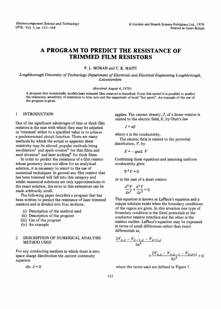
where the terms used are defined in Figure 1.
153
154 P.L. MORAN AND C. K. MAITI
(a) Small Rectangles
RiX,y+l
Vx_ ,yx+l,y
TVx,y-i
(b) Resistor Mesh
FIGURE Physical interpretation of finite differenceapproximation to LaPlace’s equation
(a) Small rectangles(b) Resistor mesh
In order to calculate Vx,y this may be rewritten as
Vx_l,y + Vx+1,y + -y (Vx, y -I + Vx,y+1)
2 1+ y(1)
Expressing the partial differential equations as smalldifferences may be shown to be equivalent to dividingthe resistor into small, equal sized rectangles wherethe voltage Vx,y is the voltage at the centre of therectangle at position (x, y); and the smaller the size ofthe rectangle the more accurate the model. In turn thismay be shown to be equivalent to representing theresistor as a two dimensional mesh of resistors, thoseresistors in the x direction being the value
hxhy
and those in the y direction
hy
hx
where p, is the sheet resistivity. The voltage Vx, y isthen the voltage at the node (x, y). Given theboundary conditions (i.e. the physical outline, positionand potential of the conductors) it is possible to
calculate an exact value for Vx,y by matrix inversion.In practice however it is preferable to use iterativetechniques to obtain an approximate solution; themagnitude of this error being set by the conditionused to terminate the iteration.
In order to reduce the computing time required,the iteration formula given in Eq. (1) may bemodified to
Vx_ + Vx+l,y + -fly (Vx,y-1 + Vx,y+l)
co + (I c) Vx,y
where w is known as the over-relaxation factor, andthe superscript is used to denote the number ofiterations so far carried out.
As previously stated, there are two distinct typesof boundary; those that define the outline of theresistor adjacent to the insulating material and thosethat interface with the conducting material. Thevoltage at the nodes adjacent to the outline boundaryis calculated by modifying the iteration formula totake into account the zero current flow normal to theresistor boundary. The voltages at the nodes on theconductor boundaries are set to fixed values, say 1.0and 0.0; the particular value depending on which ofthe two conductor boundaries the node is situated. Itshould be mentioned that the rectangles along theconductor boundaries are of only half length in thedirection normal to the conductor and it is necessaryto observe this fact when specifying a particularresistor.
The resistance is calculated by summing thecurrents flowing into one of the conductor bound-aries. If the equivalent mesh resistor in the y-directionis Ry and that in the x direction is Rx, then thecurrent flowing out of node x, y on the boundary is
&, =v,y- v,+,>, +v,y- v_,,
Rx Rx
Ry RyNotice however that (i) not all of the nodes adjacentto x,y may be defined and hence the program needsto recognise this and (ii) some of the adjacent nodesmay be part of the conductor, in which case nocurrent flows between them since they are at thesame potential.
TRIMMED FILM RESISTORS 155
The resistance R then is given by
VB1 VBO
The summation being taken over all the nodes onone conductor boundary and where VBa and VBo arethe fixed potentials of the two conductors.
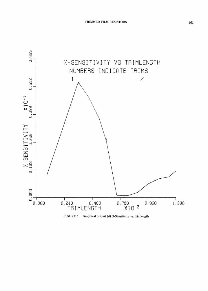
The % sensitivity is defined as
dRST 100
R dL
where L is the length of the trim.In terms of discrete values.
Rn -Rn_ 100ST Rn Ln Ln-1where the subscript refers to the calculation ofR fora trim of length Ln.
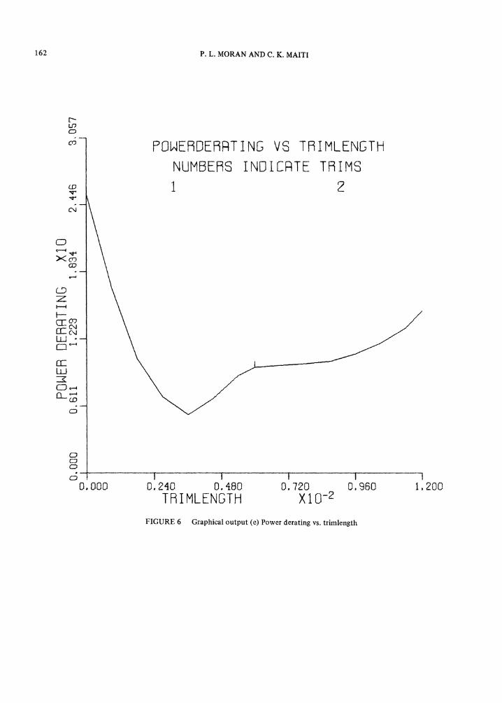
Power derating is a measure of the extent of thecurrent crowding. The power density at node x,y is
where A Vi(x,y) is the potential difference betweenthe boundaries of the rectangle surrounding nodex,y in the direction and oo is the sheet conductivity.The power dissipated in the rectangle isPxy Pxy hx hy. Thus
hy hx" AV2v(X, y)&,y zX (x, y)+
pohx pohy
,a x(X,y +
Rx RyThe total power dissipated in the resistor is
P= ,PxyThe summation being taken over all nodes. The totalpower density is
Pp=
N.hx hy’
where N is the total number of nodes. The maximumpower density is given as
Pxy maxPxy max hx hy
Thus
P PxyPxy max NPxy max
Thus if it is required to ensure that no part of theresistor dissipates more than a predetermined powerdensity, it is necessary to derate the whole resistor by
Z’PxyNPxy max
3. PROGRAM DESCRIPTION
The flow of the program can be seen to fall into threedistinct sections:-
a) setting up the nodal matrix that represents theresistor and the trim pathsb) calculating the resistance
c) plotting the results.
Due to certain program size restrictions imposedby the plotting routines used, the program has beendivided into two smaller programs that communicatevia magnetic tape units. Sections a) and b) above arecontained in the first program, whilst the results areplotted in the second.
Both subprograms require the use of large arraysand in order to allow the user, if desired, to requestonly the core store necessary, dummy array dimen-sions have been used. A listing of the master segmentsof each program is given in Appendix and theamount of core store requested is altered by changingthree statements in these segments. The variable IMXspecifies the maximum number of nodes in thex-direction and the variable JMX the maximumnumber of nodes in the y-direction. The x and ydimensions of the arrays U and IU must be specifiedas equal to IMX and JMX respectively. Provided theactual number of nodes used is less than the maximumrequested, the program will select the requiredmaximum for any particular calculation.
The variable ICONT controls the amount of lineprinter output and if it is set to O only the essentialinformation is printed, whereas if it is set to aconsiderable amount of extra information is printed.
The flow of the program is shown in Figure 2 andit can be seen that it is necessary to incorporate inthe Program Description Segments definitions of themagnetic tape units and also the plotting libraries. Alisting of the Program Description Segments is givenin Appendix 2.
156 P.L. MORAN AND C. K. MAITI
Program Data Supplied
I Calculation DataSet Up Resistor Description
Resistor Boundaries
F Set Up Trim Description
Repeatuntilfinished
Calculate Resistance
l.-------Trimpaths
Write resultsto Magnetic Tape
Program
channel channel
Read in Data
Plot Results
FIGURE 2 Flow diagram of program
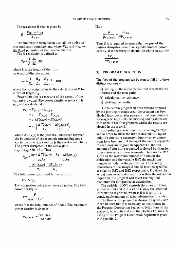
4 USE OF THE PROGRAM
allowed. Most calculations can be completed with alimit of 500 iterations. The acceleration factor (over-relaxation parameter) co has been defined already andsuitable values are 1.8 for a 10 x 10 node resistorincreasing to a maximum of 1.92 for resistors of30 x 30 nodes or greater. The distance between nodesis assumed by the program to be in units of 0.001 in.
4.2 Resistor Definition Data
The purpose of this data is to define the initial shapeof the resistor and the format for these data cards is
IDENTIFIER IX1 IY1 IX2 1Y2
The identifier, which must start in column 1, may beone of the following three types
CON1 CONO BOUN
CON1 and CONO refer to the two conductor-resistorboundaries, whilst BOUN refers to the edge of theresistor. (IX1, IY1) and (IX2, IY2) are the start andfinish respectively of the straight line, parallel to oneof the cartesian axes, that defines the outline of the
Once the system requirements of the program havebeen satisfied, the program may be used to calculatethe resistance of any particular resistor by simplychanging a few data cards. These cards can be dividedinto 3 groups which must appear in the sequence.
1) Calculation Data2) Resistor Definition Data3) Trim Definition Data
4.1 Calculation Data
Five variables must be supplied in the following order
ii)iii)
iv)
i) Maximum number of iterationsallowed per calculation
Acceleration factor 60
Distance between nodes in thex-direction
Distance between nodes in they-direction
v) Number of nodes on the trimpathbetween resistance calculations
(integer)(real)
(real)
(real)
(integer)
The data may be supplied in free format and thetype specified is given in brackets. The iterationlimit is set within the program; however it is necessaryto specify a maximum number of iterations that are FIGURE 3
Sequence
/Boundary
Trimpath
Conductor
/Boundary
Plan of resistor (dimensions in 0.001 in units)
TRIMMED FILM RESISTORS 157
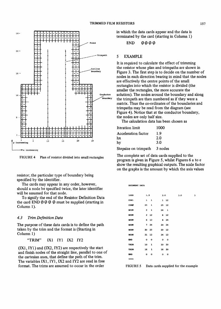
X increasing
FIGURE 4 Plan of resistor divided into small rectangles
resistor; the particular type of boundary beingspecified by the identifier.
The cards may appear in any order, however,should a node be specified twice, the later identifierwill be assumed for that node.
To signify the end of the Resistor Definition Datathe card END @ 0 g must be supplied (starting inColumn 1).
4.3 Trim Definition Data
The purpose of these data cards is to define the pathtaken by the trim and the format is (Starting inColumn 1)
"TRIM" IX1 IY1 IX2 IY2
(IX1, IY1) and (IX2, IY2) are respectively the startand finish nodes of the straight line, parallel to one ofthe cartesian axes, that define the path of the trim.The variables IX1, IY1, IX2 and IY2 are read in freeformat. The trims are assumed to occur in the order
in which the data cards appear and the data isterminated by the card (starting in Column 1)
END O 0 0 0
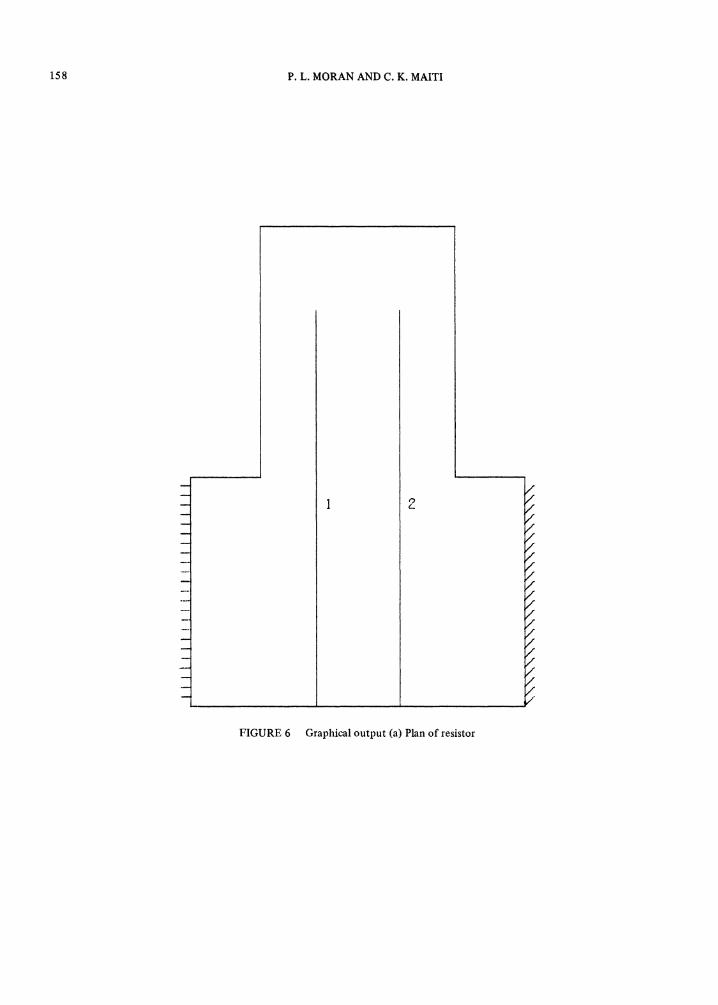
5 EXAMPLEIt is required to calculate the effect of trimmingthe resistor whose plan and trimpaths are shown inFigure 3. The first step is to decide on the number ofnodes in each direction bearing in mind that the nodesare effectively the centre points of the smallrectangles into which the resistor is divided (thesmaller the rectangles, the more accurate thesolution). The nodes around the boundary and alongthe trimpath are then numbered as if they were amatrix. Thus the co-ordinates of the boundaries andtrimpaths may be read from the diagram (seeFigure 4). Notice that at the conductor boundary,the nodes are only half size.
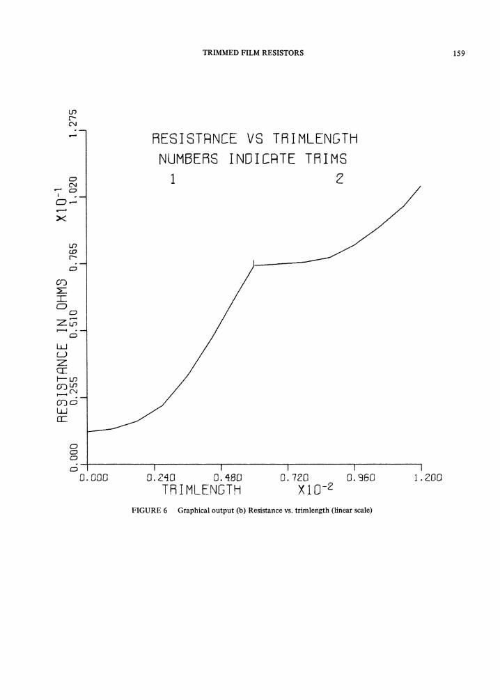
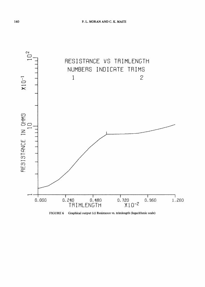
The complete set of data cards supplied to theprogram is given in Figure 5, whilst Figures 6 a to eshow the resulting graphical outputs. The scale factoron the graphs is the amount by which the axis values
DOCUMENT DATA
IOOO 1.9 .O
CON1 12
CON 25 25 12
BOUN 24
BOON 12 12
BOUN 13 24
BOUN 24 20 24
BOUN 20 23 20 12
BOUN 21 12 24 12
0 0 0 0
TRIM IO iO 20
TRIM 16 16 20
END O O O O
FIGURE 5
3.0
Data cards supplied for the example
158 P.L. MORAN AND C. K. MAITI
FIGURE 6 Graphical output (a) Plan of resistor
TRIMMED FILM RESISTORS 159
BESI 8TBNEE VS TR I MLENGTHNUMBERS I NO I CRTE TR I MS
O. 000 o. 2o o.o o.TRIMLENGTH XlO-2
O. 960 1,200
FIGURE 6 Graphical output (b) Resistance vs. trimlength (linear scale)
160 P.L. MORAN AND C. K. MAITI
RESI STANCE V8 TPI I I"ILENGTHNUHBERS I ND I CATE TPI I MS
1 2
O. 000 O. 20 O. 180 O. 720TBIHLENGTH XIO-z 1.200
FIGURE 6 Graphical output (c) Resistance vs. trimlength (logarithmic scale)
TRIMMED FILM RESISTORS 161
O, 000
X-SENSITIVITY V8 TRIHLENGTHNUMBERS I NO I ERTE TR I MS
FIGURE 6 Graphical output (d) %-Sensitivity vs. trimlength
162 P.L. MORAN AND C. K. MAITI
PIDHEEtEFtT I NI VE Tel I MLENIDTHNLIMBEFIEI I ND I EII:::tTE TF I MS1 E
O, 000 o, 20 o.0 o. 20TRIMLENGTH X10-2
960 I, 2O0
FIGURE 6 Graphical output (e) Power derating vs. trimlength
TRIMMED FILM RESISTORS 163
have been multiplied; thus 1.2 with a scale factor of10-2 is 120. The resistance function is calculated for/9 and is plotted on both linear and logarithmicscales; the most appropriate graph being used for theparticular exercise under consideration.
6 CONCLUSION
ACKNOWLEDGMENTS
We wish to acknowledge the financial support of MOD(PE)for whom this work was carried out and with whosepermission this paper is published.
We are also indebted to Mr R. G. Baker for manyhelpful comments and discussions and Dr. B. Negus of theComputer Centre, Loughborough University of Technology,for many patient hours of help.
A method of modelling laser trimmed film resistorshas been described and the various parameters thatmay be derived from it have been outlined. Thismodel has been incorporated into a computerprogram that, amongst other features, uses theminimum amount of data necessary to describe theresistor, thus reducing potential coding errors, andproduces comprehensive graphical output.
An example of the use of the program has beengiven.
REFERENCES
1. L. I. Maissel, Thin Film Resistors, in Handbdok of ThinFilm Technology, (Ed. L. I. Maissel and R. Glang).McGraw Hill, New York, pp. 18.25-18.32. 1970.
2. H. T. Law, Trimming of Thin Film Resistors by SparkErosion. Proc. 1ERE/ISHM Conference on HybridMicroelectronics, Loughborough, 1975.
3. R. E. Col, Facilities, Equipment etc. for C:’ cuitDeposition and Testing, in Handbook of Thick FilmHybrid Microelectronics, (Ed. Harper). McGraw Hill,New York, pp. 3. 33-3.41, 1975.
4. T. Cocca, et al., Laser Trimming of Thick Film Resistorsfor Military Applications. Proc. 1SHM Conference onHybrid Microelectronics, Boston 19 74.