Page 1
APSS Apollo Application Note on
Array Waveguide Grating (AWG) Design, simulation and layout
APN-APSS-AWG
Apollo Inc. 1057 Main Street West
Hamilton, Ontario L8S 1B7 Canada
Tel: (905)-524-3030 Fax: (905)-524-3050
www.apollophotonics.com
Page 2
AWG DEVICE
© Apollo Inc. Page 2 of 24 APN-APSS-AWG
Disclaimer In no event should Apollo Inc., its employees, its contractors, or the authors of this
documentation be liable to you for general, special, direct, indirect, incidental or
consequential damages, losses, costs, charges, claims, demands, or claim for lost profits,
fees, or expenses of any nature or kind.
Document Revision: July 15, 2003
Copyright © 2003 Apollo Inc.
All right reserved. No part of this document may be reproduced, modified or redistributed
in any form or by whatever means without prior written approval of Apollo Inc.
Page 3
AWG DEVICE
© Apollo Inc. Page 3 of 24 APN-APSS-AWG
Abstract
This application note describes how to design, simulate, and layout wavelength
multiplexer devices based on Array Waveguide Grating (AWG), using a pre-defined
model in the Device Module of the Apollo Photonics Solution Suite (APSS).
This application note:
• describes the operation principle, basic design considerations, and performance parameters of AWG
• presents the basic design process for AWG-based devices, based on established analytical and numerical methods
• outlines steps that are specific to the design of AWG, such as import projects, solver settings, and mask layout and export
• provides an example in order to compare simulation results with published papers
• discusses key issues related to the design of AWG-based devices, such as polarization dependence, insertion loss, cross-talk, flat-top wavelength response, and thermal control/tuning
Note: This application note focuses on using the APSS Device Module to design AWG-based devices. For more general information about other modules in the APSS, refer to other available APSS application notes. For detailed information about using the Device Module of the APSS, refer to APSS User manual.
The APSS application consists of four different modules: Material, Waveguide, Device,
and Circuit. Because each module specializes in different specific design tasks, APSS can
handle almost any kind of device made from almost any kind of material.
Keywords APSS, device module, array waveguide grating (AWG), wavelength multiplexer (MUX), wavelength demultiplexer (DeMUX), dense wavelength division multiplexing (DWDM), insertion loss, cross-talk, free spectral range
Page 4
AWG DEVICE
© Apollo Inc. Page 4 of 24 APN-APSS-AWG
Table of Contents
1 INTRODUCTION..................................................................................................... 5
2 THEORY ................................................................................................................... 6 2.1 OPERATION PRINCIPLE ......................................................................................... 6 2.2 BASIC DESIGN CONSIDERATIONS AND DESIGN PARAMETERS ................................ 8
2.2.1 Wavelength dispersion angle and distance................................................. 8 2.2.2 Free spectral range..................................................................................... 9 2.2.3 The channel spacing and focal length ........................................................ 9 2.2.4 The maximum number of the wavelength channels .................................... 9
2.3 PERFORMANCE PARAMETERS............................................................................. 10
3 DESIGN AND SIMULATION .............................................................................. 11 3.1 OVERALL DESIGN............................................................................................... 11 3.2 GENERAL DESIGN PROCEDURE ........................................................................... 12
3.2.1 Basic design parameters ........................................................................... 12 3.2.2 Channel spacing and the number of ports ................................................ 12 3.2.3 Free spectral range and the diffraction order .......................................... 12 3.2.4 Length difference ...................................................................................... 13 3.2.5 Pitches and shift positions ........................................................................ 13 3.2.6 Focusing length......................................................................................... 13 3.2.7 Number of the array waveguides .............................................................. 13 3.2.8 Other design parameters........................................................................... 14
3.3 SIMULATION AND OPTIMIZATION ....................................................................... 14
4 EXAMPLE............................................................................................................... 16 4.1 CREATION OF PREDEFINED DEVICE..................................................................... 16 4.2 SOLVER SETTINGS OF PREDEFINED DEVICE......................................................... 18 4.3 RUN AND DISPLAY............................................................................................. 20
5 DISCUSSIONS........................................................................................................ 21 5.1 POLARIZATION................................................................................................... 21 5.2 INSERTION LOSS ................................................................................................. 22 5.3 CROSS-TALK ................................................ ERROR! BOOKMARK NOT DEFINED. 5.4 FLAT-TOP WAVELENGTH RESPONSE ................................................................... 23 5.5 THERMAL CONTROL/TUNING.............................................................................. 23
6 CONCLUSION ....................................................................................................... 24
7 REFERENCES........................................................................................................ 24
Page 5
AWG DEVICE
© Apollo Inc. Page 5 of 24 APN-APSS-AWG
1 Introduction In recent years, arrayed waveguide gratings (AWG, also known as the optical phased-
array—Phasor, phased-array waveguide grating—PAWG, and waveguide grating
router—WGR) have become increasingly popular as wavelength
multiplexers/demultiplexers (MUX/DeMUX) for dense wavelength division multiplexing
(DWDM) applications [1][2]. This is due to the fact that AWG-based devices have been
proven to be capable of precisely demultiplexing a high number of channels, with
relatively low loss.
Main features of the M (input) x N (output) AWG MUX/DeMUXes are low fiber-to-fiber
loss, narrow and accurate channel spacing, large channel number, polarization
insensitivity, high stability and reliability, and being suitable for the mass production.
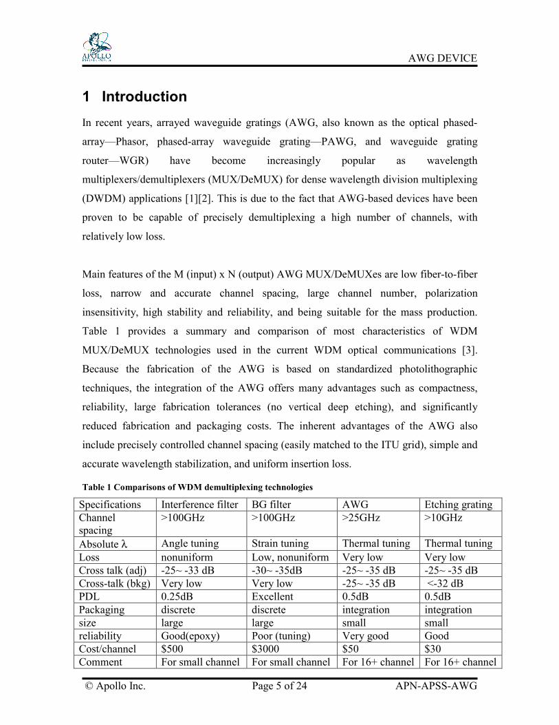
Table 1 provides a summary and comparison of most characteristics of WDM
MUX/DeMUX technologies used in the current WDM optical communications [3].
Because the fabrication of the AWG is based on standardized photolithographic
techniques, the integration of the AWG offers many advantages such as compactness,
reliability, large fabrication tolerances (no vertical deep etching), and significantly
reduced fabrication and packaging costs. The inherent advantages of the AWG also
include precisely controlled channel spacing (easily matched to the ITU grid), simple and
accurate wavelength stabilization, and uniform insertion loss.
Table 1 Comparisons of WDM demultiplexing technologies
Specifications Interference filter BG filter AWG Etching grating Channel spacing
>100GHz >100GHz >25GHz >10GHz
Absolute λ Angle tuning Strain tuning Thermal tuning Thermal tuning Loss nonuniform Low, nonuniform Very low Very low Cross talk (adj) -25~ -33 dB -30~ -35dB -25~ -35 dB -25~ -35 dB Cross-talk (bkg) Very low Very low -25~ -35 dB <-32 dB PDL 0.25dB Excellent 0.5dB 0.5dB Packaging discrete discrete integration integration size large large small small reliability Good(epoxy) Poor (tuning) Very good Good Cost/channel $500 $3000 $50 $30 Comment For small channel For small channel For 16+ channel For 16+ channel
Page 6
AWG DEVICE
© Apollo Inc. Page 6 of 24 APN-APSS-AWG
2 Theory In this section, the operation principle of the AWG devices is described [5][6]. Basic
design considerations and performance parameters for AWG-based devices are also
provided.
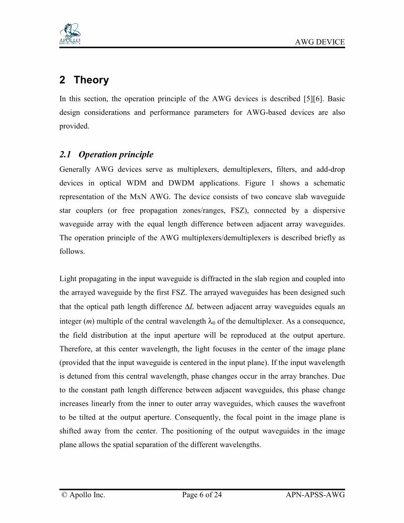
2.1 Operation principle Generally AWG devices serve as multiplexers, demultiplexers, filters, and add-drop
devices in optical WDM and DWDM applications. Figure 1 shows a schematic
representation of the MxN AWG. The device consists of two concave slab waveguide
star couplers (or free propagation zones/ranges, FSZ), connected by a dispersive
waveguide array with the equal length difference between adjacent array waveguides.
The operation principle of the AWG multiplexers/demultiplexers is described briefly as
follows.
Light propagating in the input waveguide is diffracted in the slab region and coupled into
the arrayed waveguide by the first FSZ. The arrayed waveguides has been designed such
that the optical path length difference ∆L between adjacent array waveguides equals an
integer (m) multiple of the central wavelength λ0 of the demultiplexer. As a consequence,
the field distribution at the input aperture will be reproduced at the output aperture.
Therefore, at this center wavelength, the light focuses in the center of the image plane
(provided that the input waveguide is centered in the input plane). If the input wavelength
is detuned from this central wavelength, phase changes occur in the array branches. Due
to the constant path length difference between adjacent waveguides, this phase change
increases linearly from the inner to outer array waveguides, which causes the wavefront
to be tilted at the output aperture. Consequently, the focal point in the image plane is
shifted away from the center. The positioning of the output waveguides in the image
plane allows the spatial separation of the different wavelengths.
Page 7
AWG DEVICE
© Apollo Inc. Page 7 of 24 APN-APSS-AWG
Figure 1 Schematic representation of the MxN AWG demultiplexer
Here the Gaussian beam approach (GBA), one of the analytical methods, is used to
illustrate the 1x1 imaging effect in the AWG device. The coupling coefficients Ki from
the input waveguide to the i-th arrayed waveguide are calculated by:
Ki = | f(yi,zi)|=)(z W i0
0ω exp(-)θ (ωθsinL
i2
i22
f ) Eq. 1
where θi (y=Lfsinθ and z=Lfcosθ) is the angle between the array waveguide and the
optical axis, and ω0 is the initial spot size. Due to the reciprocity, the coupling from the
FSZ to the output waveguides can be described by the same coupling coefficients.
The transfer function for an output waveguide q for an input waveguide p near the optical
axis can be obtained by summing the contributions of the different array waveguides
(assume NxN AWG with P array waveguides):
H0(λ)=∑=
P
i 1
K2i exp(jknci∆L-j q)i(p
N2π − ) Eq. 2
where coupling power Pi=K2i is the optical power in the q-th arm normalized to the total
power. The frequency response of the corresponding channels follows the result from the
overlap of this field with the modals of the output waveguides.
M Input
N Output
FSZ FSZ P, ∆L
Page 8
AWG DEVICE
© Apollo Inc. Page 8 of 24 APN-APSS-AWG
2.2 Basic design considerations and design parameters After understanding the operation principle of AWG devices, (depending on different
materials, such as silica or InP); and design requirements, such as number of channels,
wavelength spacing, and PDL, it is possible to apply some related analytical and
numerical solvers to design AWG-based devices.
2.2.1 Wavelength dispersion angle and distance The wavelength dependent shift (or wave-front tilting angle dθ) of the focal point in the
image plane can be calculated as follows:
dλ
dθ= k∆L dλ ng/(k nsλ0d ) =
dnn mn
sc
g Eq. 3
where d and ns are the propagation constant, the pitch length, and 2D effective index
in the slab waveguide, nc is the effective index in the array waveguides, ∆L is the path
length difference between adjacent array waveguides, λ0 is the center wavelength of the
AWG, and m the diffraction order of the demultiplexer defined as:
0λLnm c∆= Eq. 4
and ng is the group refractive index of array channel waveguides:
ng =(nc –λ00dλ
dnc ) =(nc –λggdλ
dn c ) Eq. 5
Using the wavelength measured in the material λg = λ0 /nc, the wavefront titling can be
simplified to:
gdλ dθ
= ds
g
nm n
, and m=gλL∆ Eq. 6
Finally, with the tilted distance dx= Lf dθ, the relative dispersion distance of the focused
spot in the image plane is determined as:
∆x = (dx/dλg) λg =Lf (dθ/dλg) λg =λg ds
fg
nmL n
Eq. 7
where Lf is the focal length of the slab waveguide.
Page 9
AWG DEVICE
© Apollo Inc. Page 9 of 24 APN-APSS-AWG
2.2.2 Free spectral range An important property of the AWG is the free spectral range (FSR), also known as the
demultiplexer periodicity. This periodicity is due to the fact that constructive interference
at the output FSZ can occur for a number of wavelengths. The free spectral range (∆λFSR,)
denotes the wavelength and frequency spacing between the maxima of the interference
pattern because of the periodic characteristic of the AWG transfer function, and can be
obtained after ignoring material dispersion of nc,
mN /λλλ 0FSR ≈∆=∆ Eq. 8
where N is the number of wavelengths or frequency channels, and ∆λ is the wavelength
channel spacing.
2.2.3 The channel spacing and focal length The wavelength channel spacing is obtained by:
∆λ= (dλdθ )-1∆θ=
g
cs
n mn d n
fLx∆ Eq. 9
where ∆x is the pitch between input and output waveguide and Lf is the focusing length
of the focusing slab waveguide. The focal length of FPZ is obtained when assuming the
ns= nc :
Lf =g
cs
n mn d n
∆λ∆x ≈
m d ns ∆λ∆x Eq. 10
2.2.4 The maximum number of the wavelength channels The maximum number of the wavelength channels N depends on the ∆λFSR: ∆λFSR ≥N∆λ
to prevent the overlapping of orders in the spectral region.
N< nc λ0/( ng m ∆λ) Eq. 11
It is found that m must be small in order to increase the number of wavelength channels.
This characteristic is the same for other multiplexers such as Mach-Zehnder
interferometers (MZI) and Fabry-Perot (FP) interferometers.
Page 10
AWG DEVICE
© Apollo Inc. Page 10 of 24 APN-APSS-AWG
2.3 Performance parameters Except some commonly used performance parameters such as insertion loss )(dBLi and
return loss )(dBLr , this section will discuss performance parameters more specifically
related to AWG-based devices. The excess loss )(dBLe of the device is defined as the
difference between the sum of the powers exiting the outputs and the power entering the
devices:
)/(log10)( 10 inj
je PPdBL ∑−= Eq. 12
As a multiplexer, two performance parameters, cross-talk and loss uniformity, should be
evaluated. The cross-talk )(dBLc is a ratio of the desired power output (Pd), to unwanted
outputs (Pu) in a channel passband. There are two types: device optical cross-talk in an
adjacent channel and optical cross-talk in a non-adjacent channel. Loss uniformity
)(dBLu is a ratio between the maximum and minimum desired outputs:
)/(log10)( 10 udc PPdBL = Eq. 13
)/(log10)( 2110 ddu PPdBL −= Eq. 14
where the cross-talk and the loss uniformity of the AWG are also evaluated by the
isolation and the power imbalance, respectively.
As an integrated component, two performance parameters, polarization dependent loss
(PDL) and ripple, should be evaluated. PDL )(dBLP is the difference in insertion loss for
one polarization compared to another. Ripple )(dBLR is the peak to peak difference in
insertion loss within one channel.
)/(log10)( 10 psP PPdBL = Eq. 15
)/(log10)( min,max,10 ddR PPdBL = Eq. 16
Page 11
AWG DEVICE
© Apollo Inc. Page 11 of 24 APN-APSS-AWG
3 Design and simulation
3.1 Overall design
This section introduces a general design procedure for creating an AWG device.
According to some related design experiences, the following process should be used:
(i) Decide the type of the AWG according to the materials and device functions.
(ii) Use a regular shaped AWG to check device performance using analytic solvers
and to determine possible sizes for the device.
(iii) Use a tapered shape and tapered port in the final design. Compared with the
regular shaped AWG device, the tapered AWG device can improve the transverse
bandwidth while keep the uniform output and loss insertion loss, as a result of the
length reduction and mode conversion in the tapered area.
(iv) Fine tune the AWG device by using the scan function and dense mesh setting in
the device simulations.
In general, the user should finish the material and waveguide design (using the Material
Module and the Waveguide Module) before starting to design an AWG device in the
Device Module.
Because AWGs are very complicated devices, consisting of straight waveguides, star
couplers, arc bend waveguides, and taper waveguides, the designer should be familiar
with the optical properties of these individual subcomponents before starting to design an
AWG device.
Note: For more general information straight waveguides, star couplers, arc bend waveguides, and taper waveguides, or for more information about the symbols used in this section, refer to other available APSS application notes or to APSS user manual.
Page 12
AWG DEVICE
© Apollo Inc. Page 12 of 24 APN-APSS-AWG
3.2 General design procedure Based on the properties calculated above, a simple design strategy can be devised and is
described below in sequence of importance. A more elaborate discussion of AWG design
aspects can be found in [6]. Of course, there are many parameters and equations that
determine the characteristics of an AWG device. This section describes the detailed
process at a high level to provide an overview.
3.2.1 Basic design parameters Before we start to design the AWG wavelength multiplexer, we should know some basic
design parameters, such as the center passband wavelength λ0, the core and cladding
effective refractive indices nc and n0 of the wafer, and the size of the core channel with
the interface. These are used to calculate the effective index ns and group refractive index
ng of array channel and slab waveguides. Some related parameters of the above values
such as the spot size ω0 can also be obtained.
3.2.2 Channel spacing and the number of ports Wavelength channel spacing ∆λ and the number of the wavelength channels M and N are
the most important parameters to design the AWG wavelength multiplexer. Usually the
wavelength channel spacing ∆λ is selected according to the ITU-grid standard such as 50
GHz, 100 GHz, or 200 GHz. The numbers of the wavelength channels M are determined
according to the requirements of the WDM/DWDM network and its customers. Generally
there are two kinds of AWG: 1xN (M=1) and NxN (M=N). The number of the wavelength
channels N is selected with the exponent of 2 such as 16, 32, 64, and 128.
3.2.3 Free spectral range and the diffraction order After obtaining the wavelength channel spacing ∆λ and the number of the wavelength
channels N, the wavelength free spectral ranges ∆λFSR is easily calculated:
∆λFSR = N∆λ Eq. 17
and the diffraction order m is calculated as:
m < nc λ0/[ ng N ∆λ] or m=floor(FSR
c
λλ
∆) Eq. 18
Page 13
AWG DEVICE
© Apollo Inc. Page 13 of 24 APN-APSS-AWG
The flooring of the nearest integer is necessary to fix the center wavelength to the
specified value. Note that this will lead to a slight correction of the FSR.
3.2.4 Length difference Length difference ∆L between the neighboring arrayed waveguides is calculated by:
∆L = mc
0
nλ
Eq. 19
3.2.5 Pitches and shift positions In general, the shift positions ∆x and pitches d should be as small as possible to obtain a
compact design for the AWG MUX/DeMUX. In order to achieve sufficient isolation
between neighbor output waveguides, the gap between the output waveguides should be
sufficiently large. As a general rule, this gap should be twice the width of the waveguide.
With the output waveguide spacing fixed, the relative dispersion ∆x can be calculated to
be:
∆x = d λ0 /∆λ Eq. 20
where ∆λ is the channel spacing of the demultiplexer.
3.2.6 Focusing length As long as the array order has been fixed, the focal length Lf can be calculated:
Lf =g
cs
n mn d n
∆λ∆x ≈
m d ns ∆λ∆x =
m d ns ∆λ∆x Eq. 21
3.2.7 Number of the array waveguides The number of the array waveguides P is not a dominant parameter in the AWG design
because the ∆λ and N do not depend on it. Generally, P is selected so that the number of
array waveguides is sufficient to make the numerical aperture (NA), in which they form a
greater number than the input/output waveguides, such that almost all the light diffracted
into the free space region is collected by the array aperture. As a general rule, this number
should be bigger than four times the number of wavelength channels.
P=(4-6)*max(M,N) Eq. 22
Page 14
AWG DEVICE
© Apollo Inc. Page 14 of 24 APN-APSS-AWG
3.2.8 Other design parameters The current design still has several areas for design decisions, such as the taper length Lt,
L3, and L4, which may be used to optimize the design. To determine the minimum radius
of the device bend, the phase velocity of exponential tails of the mode profile should be
less than that of the cladding layer:
rn
cR
2/wR eff+ <0n
c , or Rmin> 2
w eff [0
r
nn -1] -1=
∆2w eff Eq. 23
where nr, n0, and ∆ are the core, cladding indices, and index difference, and weff is the
effective waveguide width. We can find that the waveguide bend with a tight mode
confinement and a larger index difference has a small-bend radius. The input/output port
pitch d1/d2 can be determined by the optical fiber diameter, for example, 250 µm for the
single mode optical fiber.
3.3 Simulation and optimization This section provides an overview of the simulation and optimization process performed
using the APSS Device Module.
Although an AWG device is typically complex, the Device Module provides a user-
friendly wizard that can be used to build an AWG device based on a pre-defined model.
After loading the waveguide information and selecting “Device type” as “AWG”, the
wizard asks the user to enter some information related to the device ports, star couplers,
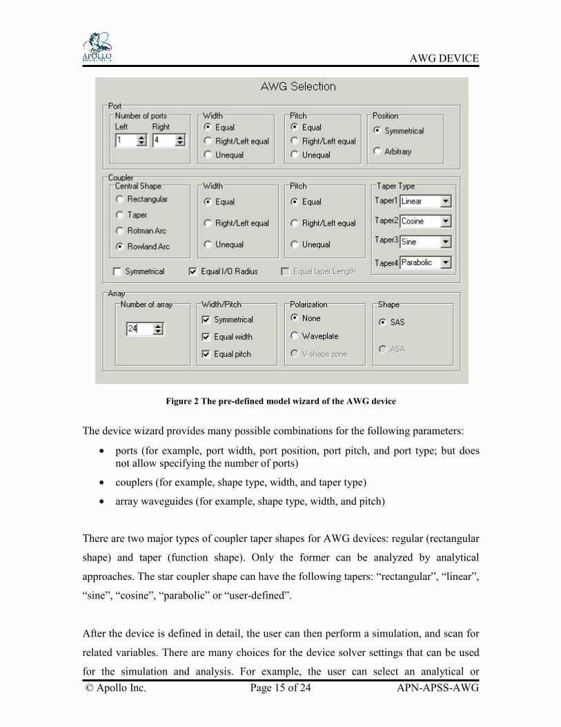
and array waveguides, as shown in Figure 2.
Page 15
AWG DEVICE
© Apollo Inc. Page 15 of 24 APN-APSS-AWG
Figure 2 The pre-defined model wizard of the AWG device
The device wizard provides many possible combinations for the following parameters:
• ports (for example, port width, port position, port pitch, and port type; but does not allow specifying the number of ports)
• couplers (for example, shape type, width, and taper type)
• array waveguides (for example, shape type, width, and pitch)
There are two major types of coupler taper shapes for AWG devices: regular (rectangular
shape) and taper (function shape). Only the former can be analyzed by analytical
approaches. The star coupler shape can have the following tapers: “rectangular”, “linear”,
“sine”, “cosine”, “parabolic” or “user-defined”.
After the device is defined in detail, the user can then perform a simulation, and scan for
related variables. There are many choices for the device solver settings that can be used
for the simulation and analysis. For example, the user can select an analytical or
Page 16
AWG DEVICE
© Apollo Inc. Page 16 of 24 APN-APSS-AWG
numerical solver, without or with tapers. In general, for a strongly guided AWG device,
an analytical solver is sufficient for most applications.
Finally, the user can display the simulation results to view the different performance
parameters such as insertion loss, phase difference, and cross-talk. The user can also
export them in different formats such as ASCII text (*.txt), Microsoft Excel (*.xls), or as
a bitmap (*.bmp) file. The layout mask files can be exported in two different file formats:
EXF and GDSII.
4 EXAMPLE This section provides an example outline of the process for the creation and simulation of
a typical silica AWG, using the equivalent index of a 3D waveguide. This section also
demonstrates how the flexible simulation and scan function enables the optical designer
to efficiently and effectively perform sensitivity analysis of an AWG device, related to
length, polarization, wavelength dependence, port width effect, FSZ width, FSZ taper,
and coupler pitch.
4.1 Creation of predefined device In order to illustrate the design and simulation concepts outlined in the previous chapters,
the example used is for an 1x16 AWG with the design parameters specified in the
following references: [7], [8].
The user selects “user-input” and selects a predefined “AWG” (as shown in Figure 2)
where M=1 (number of input ports), N=16 (number of output ports), P = 60 (number of
array waveguides), and all other values remaining set at the default settings
(“Symmetrical”, “Equal”, and “None” for the port, coupler, and array, respectively). The
user then clicks “Next”, and on the following window, changes the necessary design
parameters. The user clicks “Finish” to create the device project (which, in this example,
is named “D_AWG1x16x60”). Note that the corresponding equivalent indices (1.4551 of
core and 1.4441 of cladding) can be input here as shown in Figure 3. The layout and
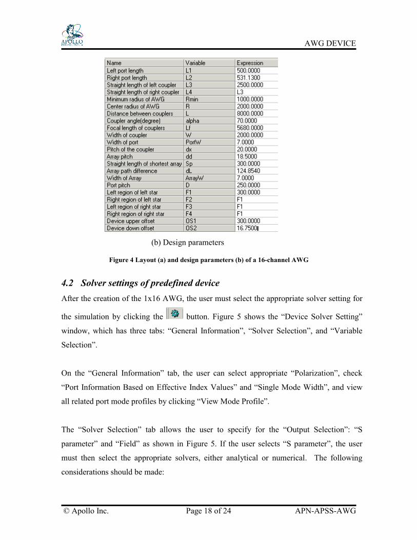
detailed design parameters can be obtained as shown in Figure 4(a) and Figure 4 (b),
Page 17
AWG DEVICE
© Apollo Inc. Page 17 of 24 APN-APSS-AWG
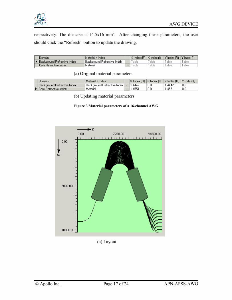
respectively. The die size is 14.5x16 mm2. After changing these parameters, the user
should click the “Refresh” button to update the drawing.
(a) Original material parameters
(b) Updating material parameters
Figure 3 Material parameters of a 16-channel AWG
(a) Layout
Page 18
AWG DEVICE
© Apollo Inc. Page 18 of 24 APN-APSS-AWG
(b) Design parameters
Figure 4 Layout (a) and design parameters (b) of a 16-channel AWG
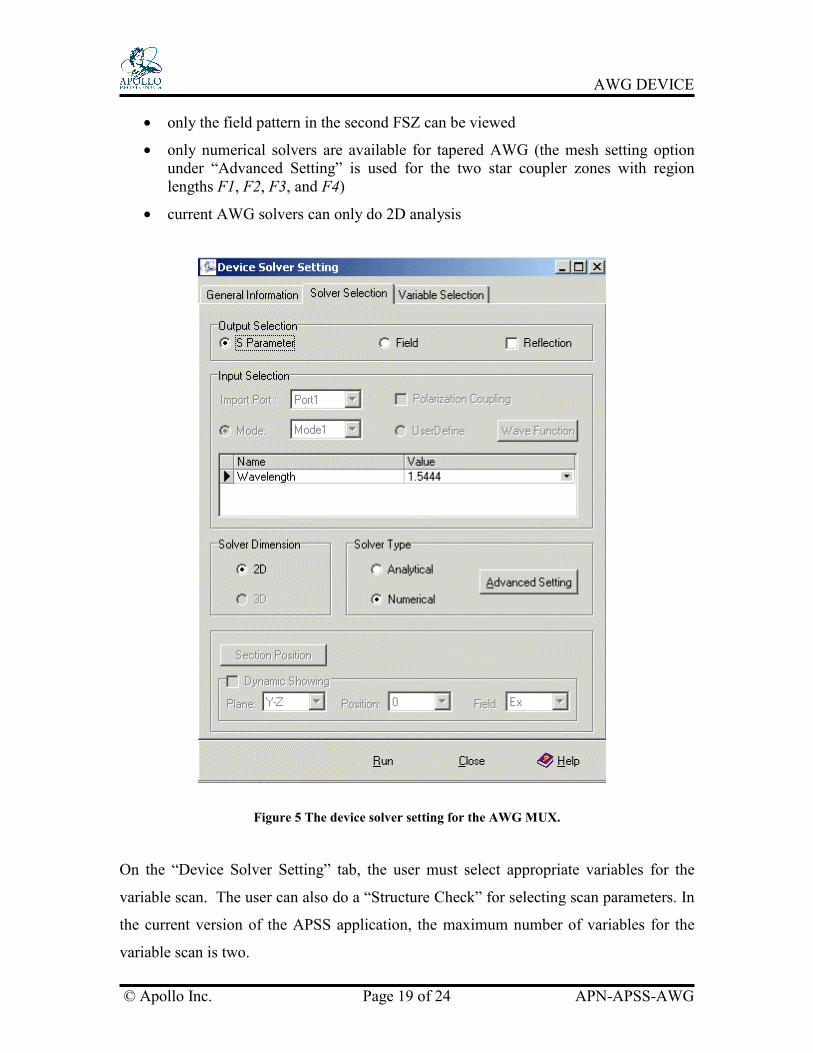
4.2 Solver settings of predefined device After the creation of the 1x16 AWG, the user must select the appropriate solver setting for
the simulation by clicking the button. Figure 5 shows the “Device Solver Setting”
window, which has three tabs: “General Information”, “Solver Selection”, and “Variable
Selection”.
On the “General Information” tab, the user can select appropriate “Polarization”, check
“Port Information Based on Effective Index Values” and “Single Mode Width”, and view
all related port mode profiles by clicking “View Mode Profile”.
The “Solver Selection” tab allows the user to specify for the “Output Selection”: “S
parameter” and “Field” as shown in Figure 5. If the user selects “S parameter”, the user
must then select the appropriate solvers, either analytical or numerical. The following
considerations should be made:
Page 19
AWG DEVICE
© Apollo Inc. Page 19 of 24 APN-APSS-AWG
• only the field pattern in the second FSZ can be viewed
• only numerical solvers are available for tapered AWG (the mesh setting option under “Advanced Setting” is used for the two star coupler zones with region lengths F1, F2, F3, and F4)
• current AWG solvers can only do 2D analysis
Figure 5 The device solver setting for the AWG MUX.
On the “Device Solver Setting” tab, the user must select appropriate variables for the
variable scan. The user can also do a “Structure Check” for selecting scan parameters. In
the current version of the APSS application, the maximum number of variables for the
variable scan is two.
Page 20
AWG DEVICE
© Apollo Inc. Page 20 of 24 APN-APSS-AWG
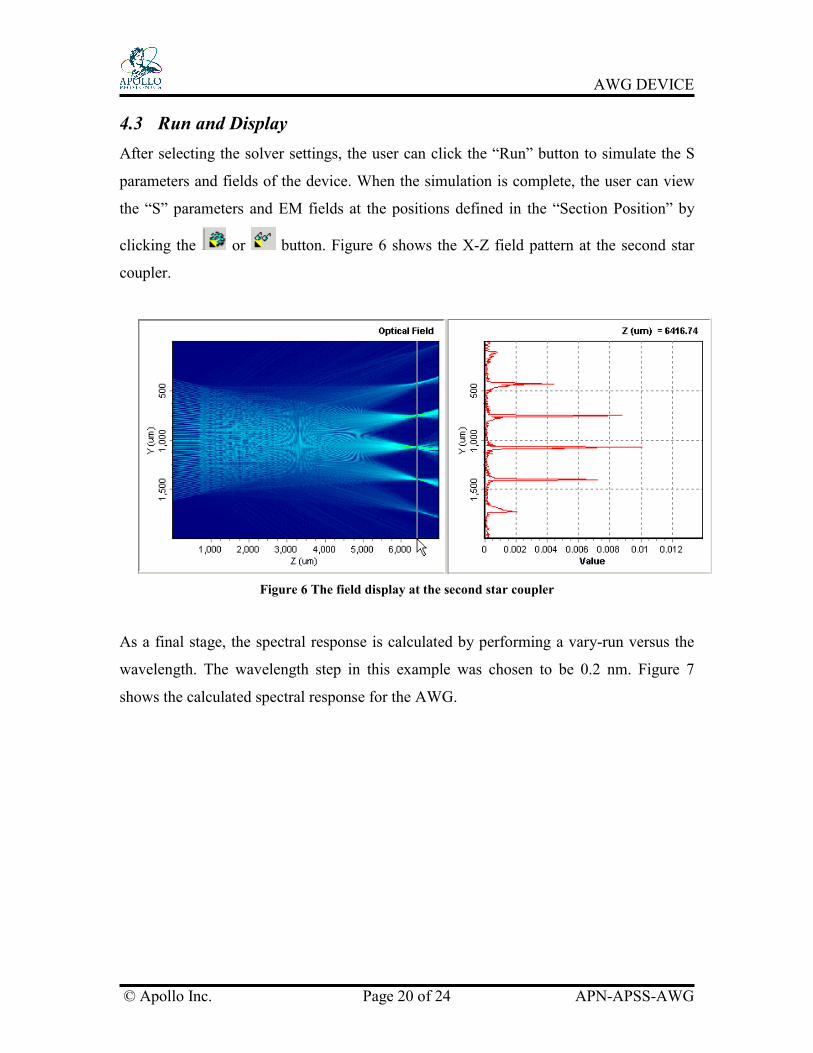
4.3 Run and Display After selecting the solver settings, the user can click the “Run” button to simulate the S
parameters and fields of the device. When the simulation is complete, the user can view
the “S” parameters and EM fields at the positions defined in the “Section Position” by
clicking the or button. Figure 6 shows the X-Z field pattern at the second star
coupler.
Figure 6 The field display at the second star coupler
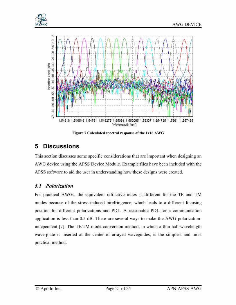
As a final stage, the spectral response is calculated by performing a vary-run versus the
wavelength. The wavelength step in this example was chosen to be 0.2 nm. Figure 7
shows the calculated spectral response for the AWG.
Page 21
AWG DEVICE
© Apollo Inc. Page 21 of 24 APN-APSS-AWG
Figure 7 Calculated spectral response of the 1x16 AWG
5 Discussions This section discusses some specific considerations that are important when designing an
AWG device using the APSS Device Module. Example files have been included with the
APSS software to aid the user in understanding how these designs were created.
5.1 Polarization For practical AWGs, the equivalent refractive index is different for the TE and TM
modes because of the stress-induced birefringence, which leads to a different focusing
position for different polarizations and PDL. A reasonable PDL for a communication
application is less than 0.5 dB. There are several ways to make the AWG polarization-
independent [7]. The TE/TM mode conversion method, in which a thin half-wavelength
wave-plate is inserted at the center of arrayed waveguides, is the simplest and most
practical method.
Page 22
AWG DEVICE
© Apollo Inc. Page 22 of 24 APN-APSS-AWG
5.2 Insertion loss In WDM communications, it is very important for the AWG device to have low fiber-to-
fiber loss. The main sources for the AWG insertion loss are:
• the propagation loss of bent waveguides
• the coupling loss between the fiber and the waveguide
• the transition loss between the star coupler and arrayed waveguides
• the material and scattering losses of silica
In practice, large radii and tapered transition (for example, horizontal and vertical tapers)
are used, rendering bend loss negligible. Research groups have reported loss among 2.3–
2.7 dB. Commercially available AWGs have a 4.5 dB loss for Gaussian passbands and
7.0 dB for flat top passbands.
5.3 Cross-talk According to the review paper [4], there are many mechanisms that can cause cross-talk.
Six sources are: receiver cross-talk, truncation, mode conversion, coupling in the array,
phase transfer incoherence, and background radiation. The first four can be kept low
through effective design.
The most obvious source of the cross-talk is caused by the coupling between the receiver
sides of the star coupler. Using the overlap between the exponential tails of the
propagation field and the waveguide mode profile, the cross-talk can be easily calculated.
Another source of cross-talk is caused from truncation of the propagation field by the
finite width of the output array aperture. This truncation of the field produces the loss of
energy and increases the output focal field side-lobe level. To obtain sufficiently low
cross-talk, the array aperture angle of AWG should be larger than twice the Gaussian
width of the field. The truncation cross-talk should be less than –35dB when this
requirement is met.
Page 23
AWG DEVICE
© Apollo Inc. Page 23 of 24 APN-APSS-AWG
Cross-talk by mode conversion is caused by a “ghost” image of multimode junctions. It
can be kept low by optimizing the junction offset by avoiding first mode excitation.
The cross-talk caused by coupling in the array can be avoided by increasing the distance
between the arrayed waveguide. However, due to imperfections of the fabrication
process, the incoherence of the phased array, caused by the change of optical path length
(in the order of thousands of wavelengths), may lead to considerable phased error, and,
consequently, to increase the cross-talk. For this reason, on a practical level, the reduction
of cross-talk for an AWG device is limited by imperfection in the fabrication process.
5.4 Flat-top wavelength response In many applications, the flat-top passband is very important to relax the wavelength
control requirements. There are several approaches that can be used to achieve this goal.
The most simple method is to use multimode waveguides at the receiver side of the
AWG. If the focal spot moves along these broad waveguides, almost 100% of the light is
coupled into the receiver to have a flat region in the frequency response, in which the 1
dB bandwidth can be easily increased from 31% of the channel spacing to 65%. Another
method is to apply a short MMI power splitter or a Y-junction (two output branches close
together) at the end of the transmitter waveguide of the star coupler. The operation
principle of such a device is to convert the single waveguide mode into the double
(camel-like) image, and, consequently, to flatten the frequency response because the
AWG is a 1:1 image system.
5.5 Thermal control/tuning In order to use AWG devices in practical optical communication applications, precise
wavelength control and long-term wavelength stability are needed. Of course, a channel
wavelength will change according to the thermal coefficient of the material used, if the
temperature of AWG fluctuates. By making use of the thermo-optic (TO) effect, a
temperature controller can be built into the AWG to control and tune the device to the
ITU grid or other desired wavelength.
Page 24
AWG DEVICE
© Apollo Inc. Page 24 of 24 APN-APSS-AWG
6 Conclusion As demonstrated with a practical example, APSS offers designers a feasible and efficient
way to design and simulate an AWG device. This can be accomplished by taking
advantage of the knowledge-based, pre-defined model in the APSS Device Module to
create an effective, functional design. The theory and operational principle of the AWG
device have been described. Finally, the design process has been outlined, and the
simulation results agree well with experimental results.
7 References [1] A. R. Vellekoop and M. K. Smit, “Four channel integrated-optic wavelength
multiplexer with weak polarization dependence,” J. Lightwave Technol., vol. 9, no. 3,
pp. 310-314, 1991.
[2] C. Dragone, “An NxN optical multiplexer using a planar arrangement of two star
couplers,” IEEE Phot. Techn. Lett., vol. 3, no. 9, pp. 812-815, 1991.
[3] E. S. Koteles, “Integrated planar waveguide demultiplexers for high density WDM
applications,” Fiber and Integrated Optics, vol.18, pp. 211-244, 1999.
[4] M. K. Smit and C. van Dam, "PHASAR-Based WDM-Devices: Principles, Design
and Applications", IEEE J. of Sel. Topics in Q.E., vol. 2, no. 2, pp. 236-250, 1996.
[5] A. Kaneko et al, “Recent progress on AWGs for DWDM applications,” IEICE trans.
Vol.E83-C, no.6, 860-868, 2000.
[6] H. Takahashi, “Arrayed waveguide grating for wavelength division multiplexer with
nanometer resolution,” Electron. Lett., vol. 26, pp. 87-88, 1990.
[7] Y. Inoue, H. Takahashi, and et al: “Elimination of polarization sensitivity in silica-
based wavelength division multiplexer using a polyimide half waveplate,” J.
Lightwave Technol., vol.15, no.3, pp1947-1957, 1997.
[8] K. Okamoto, Fundamentals of optical waveguides, New York: Academic, pp. 359,
2000.