©2018 Littelfuse, Inc.Specifications are subject to change without notice.
TVS Diode Arrays (SPA ® Diodes)
Revision: 02/14/18
TVS Diode Arrays (SPA® Diodes)
SPHV Series
General Purpose ESD Protection - SPHV Series
Description
Applications
The AQHV series is designed to provide an option for very fast acting, high performance over-voltage protection devices. Ideally suited for power interfaces, passenger charging interfaces, and well as LED lighting modules, and low speed I/Os. It will protect sensitive equipment from damage due to electrostatic discharge (ESD) and other overvoltage transients.
The AQHV series can safely absorb repetitive ESD strikes above the maximum level of the IEC 61000-4-2 international standard (Level 4, ±8kV contact discharge) without performance degradation and safely conduct up to 8A (AQHV12) of induced surge current (IEC 61000-4-5 2nd edition, tP=8/20μs) with very low clamping voltages.
Features
• ESD, IEC 61000-4-2,
±30kV contact, ±30kV air
• EFT, IEC 61000-4-4, 40A
(5/50ns)
• Lightning, 8A (8/20 as defined in IEC 61000-4-5 2nd edition) for AQHV12
• Low clamping voltage
• PPAP capable
• Low leakage current
• Small SOD882 packaging helps save board space
• AEC-Q101 qualified
• Moisture Sensitivity Level(MSL -1)
• Halogen free, lead free and RoHS compliant
• LED Lighting Modules
• Portable Instrumentation
• General Purpose I/O
• RS232 / RS485
• CAN and LIN Bus
• Automotive application
RoHS Pb GREENAQHV Series 200W Discrete Unidirectional TVS Diode
Pinout
Functional Block Diagram
1
2
Life Support Note:
Not Intended for Use in Life Support or Life Saving Applications
The products shown herein are not designed for use in life sustaining or life saving applications unless otherwise expressly indicated.
1
2
AQHV Series
©2018 Littelfuse, Inc.Specifications are subject to change without notice.
TVS Diode Arrays (SPA ® Diodes)
Revision: 02/14/18
TVS Diode Arrays (SPA® Diodes)
SPHV Series
General Purpose ESD Protection - SPHV Series
Notes:
CAUTION: Stresses above those listed in “Absolute Maximum Ratings” may cause permanent damage to the component. This is a stress only rating and operation of the component at these or any other conditions above those indicated in the operational sections of this specification is not implied.
Absolute Maximum Ratings
Symbol Parameter Value Units
Ppk Peak Pulse Power (tp=8/20μs) 200 W
TOP Operating Temperature -40 to 150 °C
TSTOR Storage Temperature -55 to 150 °C
AQHV12 Electrical Characteristics (TOP=25ºC)
Parameter Symbol Test Conditions Min Typ Max Units
Reverse Standoff Voltage VRWM IR≤1μA 12.0 V
Breakdown Voltage VBR IR=1mA 13.3 V
Leakage Current ILEAK VR=12V 1.0 μA
Clamp Voltage1 VC
IPP=1A, tp=8/20µs, Fwd 19.0 V
IPP=8A, tP=8/20μs, Fwd 25.0 V
Dynamic Resistance2 RDYN TLP, tp=100ns, I/O to GND 0.37 Ω
Peak Pulse Current Ipp tp=8/20µs 8.0 A
ESD Withstand Voltage1 VESD
IEC 61000-4-2 (Contact Discharge) ±30 kV
IEC 61000-4-2 (Air Discharge) ±30 kV
Diode Capacitance1 CD-GND Reverse Bias=0V, f=1MHz 60 pF
AQHV15 Electrical Characteristics (TOP=25ºC)
Parameter Symbol Test Conditions Min Typ Max Units
Reverse Standoff Voltage VRWM IR≤1μA 15.0 V
Breakdown Voltage VBR IR=1mA 16.7 V
Leakage Current ILEAK VR=15V 1.0 μA
Clamp Voltage1 VC
IPP=1A, tp=8/20µs, Fwd 22.0 V
IPP=5A, tp=8/20µs, Fwd 28.0 V
Dynamic Resistance2 RDYN TLP, tp=100ns, I/O to GND 0.40 Ω
Peak Pulse Current Ipp tp=8/20µs 5.0 A
ESD Withstand Voltage1 VESD
IEC 61000-4-2 (Contact Discharge) ±30 kV
IEC 61000-4-2 (Air Discharge) ±30 kV
Diode Capacitance1 CI/O-GND Reverse Bias=0V, f=1MHz 46 pF
AQHV Series
©2018 Littelfuse, Inc.Specifications are subject to change without notice.
TVS Diode Arrays (SPA ® Diodes)
Revision: 02/14/18
TVS Diode Arrays (SPA® Diodes)
SPHV Series
General Purpose ESD Protection - SPHV Series
AQHV24 Electrical Characteristics (TOP=25ºC)
Parameter Symbol Test Conditions Min Typ Max Units
Reverse Standoff Voltage VRWM IR≤1μA 24.0 V
Breakdown Voltage VBR IR=1mA 26.7 V
Leakage Current ILEAK VR=24V 1.0 μA
Clamp Voltage1 VC
IPP=1A, tp=8/20µs, Fwd 36.0 V
IPP=3A, tp=8/20µs, Fwd 50.0 V
Dynamic Resistance2 RDYN TLP, tp=100ns, I/O to GND 0.56 Ω
Peak Pulse Current Ipp tp=8/20µs 3.0 A
ESD Withstand Voltage1 VESD
IEC 61000-4-2 (Contact Discharge) ±24 kV
IEC 61000-4-2 (Air Discharge) ±30 kV
Diode Capacitance1 CI/O-GND Reverse Bias=0V, f=1MHz 32 pF
AQHV36 Electrical Characteristics (TOP=25ºC)
Parameter Symbol Test Conditions Min Typ Max Units
Reverse Standoff Voltage VRWM IR≤1μA 36.0 V
Breakdown Voltage VBR IR=1mA 40.0 V
Leakage Current ILEAK VR=36V 1.0 μA
Clamp Voltage1 VC
IPP=1A, tp=8/20µs, Fwd 52.0 V
IPP=2A, tp=8/20µs, Fwd 60.0 V
Dynamic Resistance2 RDYN TLP, tp=100ns, I/O to GND 1.28 Ω
Peak Pulse Current Ipp tp=8/20µs 2.0 A
ESD Withstand Voltage1 VESD
IEC 61000-4-2 (Contact Discharge) ±15 kV
IEC 61000-4-2 (Air Discharge) ±20 kV
Diode Capacitance1 CI/O-GND Reverse Bias=0V, f=1MHz 25 pF
Non-Repetitive Peak Pulse Power vs. Pulse Time
Pulse Duration - tp (µs)
Pea
k Pu
lse
Po
wer
- P
pk
(kW
)
0.01
0.1
1
10
0.1 1 10 100 1000
Power Derating Curve
0
10
20
30
40
50
60
70
80
90
100
110
0 25 50 75 100 125 150
Ambient Temperature - TA (oC)
% o
f R
ated
Po
wer
IPP
Note:1 Parameter is guaranteed by design and/or component characterization. 2 Transmission Line Pulse (TLP) with 100ns width, 2ns rise time, and average window t1=70ns to t2= 90ns
AQHV Series
©2018 Littelfuse, Inc.Specifications are subject to change without notice.
TVS Diode Arrays (SPA ® Diodes)
Revision: 02/14/18
TVS Diode Arrays (SPA® Diodes)
SPHV Series
General Purpose ESD Protection - SPHV Series
8/20μs Pulse Waveform
0%
10%
20%
30%
40%
50%
60%
70%
80%
90%
100%
110%
0.0 5.0 10.0 15.0 20.0 25.0 30.0
Time (μs)
Per
cen
t o
f I P
P
0
2
4
6
8
10
12
14
16
18
20
0 5 10 15 20 25
TLP Voltage (V)
TLP
Curr
ent (
A)
AQHV12 Transmission Line Pulsing(TLP) Plot
0
2
4
6
8
10
12
14
16
18
20
0 5 10 15 20 25 30
TLP Voltage (V)
TLP
Curr
ent (
A)
AQHV15 Transmission Line Pulsing(TLP) Plot
0
2
4
6
8
10
12
14
16
18
20
0 5 10 15 20 25 30 35 40 45
TLP Voltage (V)
TLP
Curr
ent (
A)
AQHV24 Transmission Line Pulsing(TLP) Plot
0
2
4
6
8
10
12
14
16
0 10 20 30 40 50 60 70 80 90 100
TLP Voltage (V)
TLP
Curr
ent (
A)
AQHV36 Transmission Line Pulsing(TLP) Plot
AQHV Series
©2018 Littelfuse, Inc.Specifications are subject to change without notice.
TVS Diode Arrays (SPA ® Diodes)
Revision: 02/14/18
TVS Diode Arrays (SPA® Diodes)
SPHV Series
General Purpose ESD Protection - SPHV Series
Time
Tem
pera
ture
TP
TLTS(max)
TS(min)
25
tP
tL
tS
time to peak temperature
PreheatPreheat
Ramp-upRamp-up
Ramp-downRamp-do
Critical ZoneTL to TPCritical ZoneTL to TP
Reflow Condition Pb – Free assembly
Pre Heat
- Temperature Min (Ts(min)) 150°C
- Temperature Max (Ts(max)) 200°C
- Time (min to max) (ts) 60 – 180 secs
Average ramp up rate (Liquidus) Temp (TL) to peak
3°C/second max
TS(max) to TL - Ramp-up Rate 3°C/second max
Reflow- Temperature (TL) (Liquidus) 217°C
- Temperature (tL) 60 – 150 seconds
Peak Temperature (TP) 260+0/-5 °C
Time within 5°C of actual peak Temperature (tp)
20 – 40 seconds
Ramp-down Rate 6°C/second max
Time 25°C to peak Temperature (TP) 8 minutes Max.
Do not exceed 260°C
Soldering Parameters
Ordering Information
Part Number Package Marking Min. Order Qty.
AQHV12-01ETG
SOD882
U2
10000AQHV15-01ETG U5
AQHV24-01ETG U4
AQHV36-01ETG U6
Part Numbering System
Part Marking System
AQHV ** 01 T G
Voltage
Number ofChannels Package
T= Tape & Reel
G= Green
–
TVS Diode Arrays(SPA® AutomotiveGrade Diodes)
E: SOD882
E – C
Bidirectional
U*
2: SPHV125: SPHV154: SPHV246: SPHV36
1 2
AQHV Series
2: AQHV125: AQHV154: AQHV246: AQHV36
Product Characteristics
Lead Plating Pre-Plated Frame
Lead Material Copper Alloy
Substrate material Silicon
Body Material Molded Compound
Flammability UL Recognized compound meeting flammability rating V-0
Notes : 1. All dimensions are in millimeters2. Dimensions include solder plating.3. Dimensions are exclusive of mold flash & metal burr.
©2018 Littelfuse, Inc.Specifications are subject to change without notice.
TVS Diode Arrays (SPA ® Diodes)
Revision: 02/14/18
TVS Diode Arrays (SPA® Diodes)
SPHV Series
General Purpose ESD Protection - SPHV Series
Embossed Carrier Tape & Reel Specification
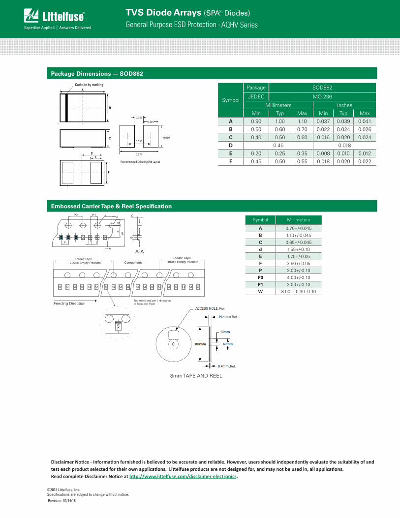
Feeding DirectionTop mark and pin 1 direction in Tape and Reel
UX
1
2
Symbol Millimeters
A 0.70+/-0.045
B 1.10+/-0.045
C 0.65+/-0.045
d 1.55+/-0.10
E 1.75+/-0.05
F 3.50+/-0.05
P 2.00+/-0.10
P0 4.00+/-0.10
P1 2.00+/-0.10
W 8.00 + 0.30 -0.10
Package Dimensions — SOD882
Cathode by marking
Recommended Soldering Pad Layout
0.3250.325
0.650
0.975
0.650
Symbol
Package SOD882
JEDEC MO-236
Millimeters Inches
Min Typ Max Min Typ Max
A 0.90 1.00 1.10 0.037 0.039 0.041
B 0.50 0.60 0.70 0.022 0.024 0.026
C 0.40 0.50 0.60 0.016 0.020 0.024
D 0.45 0.018
E 0.20 0.25 0.35 0.008 0.010 0.012
F 0.45 0.50 0.55 0.018 0.020 0.022
AQHV Series
,Ref.
,Ref.
,Ref.
8mm TAPE AND REEL
Disclaimer Notice - Information furnished is believed to be accurate and reliable. However, users should independently evaluate the suitability of and test each product selected for their own applications. Littelfuse products are not designed for, and may not be used in, all applications. Read complete Disclaimer Notice at http://www.littelfuse.com/disclaimer-electronics.