Page 1
0
Arash Fouladi Azarnaminy
INDUCTIVE BUCK CONVERTER BASED ON LOW VOLTAGE NANO-SCALE CMOS Master of Science Thesis
Supervisor: Professor Nikolay T.
Tchamov, Ph. D
Examiner: Prof. Nikolay T. Tchamov
and Jani Järvenhaara
Examiners and subjects were ap-
proved in the Faculty of Computing
and Electrical Engineering Council
meeting on 13-Aug-2014
Page 2
I
ABSTRACT
TAMPERE UNIVERSITY OF TECHNOLOGY
Master’s Degree Programme in Electrical Engineering
ARASH FOULADI AZARNAMINY: Inductive Buck Converter Based on Low
Voltage Nano-Scale CMOS
Masters of Science Thesis, 59 pages and 1 Appendix page
Sep 2015
Major: Radio Frequency Electonics
Supervisor: Prof. Nikolay T. Tchamov, Ph. D
Examiners: Prof. Nikolay T. Tchamov and Jani Järvenhaara
Keywords: Buck Converter, Cascode, CMOS, 45nm
Cascode architecture is an efficient and cost effective design technique to overcome the
reliability issues regarding Gate-Oxide breakdown. This method is employed for cir-
cuits such as DC-DC converters and power amplifiers operating with input supply volt-
age higher than transistor breakdown voltage. Design of the gate bias circuit which con-
trols the switching operation of the power stage transistors is the main challenge in this
technique, especially for the power stage with more than two stacked transistors. The
bias circuit generates the required gate drive signals with proper timing to avoid the
voltage stress condition.
This thesis presents design and simulation results of the buck type DC-DC converter
based on 45nm CMOS technology. Breakdown voltage of the transistor is 1.1V. There-
fore, 6-stacked power stage configuration is proposed for a fixed input voltage of 6V by
considering a maximum supply voltage of 1V for each transistor. Switching operation
of the power stage is controlled by driving signals for PMOS and NMOS stacked tran-
sistors. In order to generate the driver signal, three cascade stages of high speed level
shifters are employed to shift up the driver signal by 5V. Switching frequency is 52MHz
and open loop control scheme is considered for the buck converter. The control circuit
consists of a Schmitt trigger and a Non-Overlapping switching circuit to generate the
driving signals with adjusted dead times. The designed buck converter provides an out-
put voltage of 1.25V and has an efficiency of 79.2% with a fixed input power of
207mW. A second buck converter circuit is also presented that operates under variable
battery voltages from 3.5V to 6V. Using the designed circuit the output voltage is 1.25V
and a maximum power conversion efficiency of 81.3% is obtained for an input voltage
of 3.9V. The output power is 200mW and a high power density of 195mW/mm3
is
achieved
Page 3
II
PREFACE
This thesis work was done in RF Integrated Circuit group (RFIC), Department of Elec-
tronics and Communication at Tampere University of Technology for the partial ful-
fillment of the requirements for degree of Master of Science in Electrical Engineering.
The research work was financially supported by Academy of Finland.
Foremost, I would like to acknowledge my supervisor, Prof. Nikolay T. Tchamov who
gave me the great opportunity to start working in RFIC lab. His guidance and advices
have had a major impact on thesis outcome. I am also grateful to other members of
RFIC group. Especially, I would like to thank Jani Järvenhaara for his valuable guid-
ance during research work.
Finally, I am grateful to my parents and brothers for their endless support and encour-
agement that made all of this possible.
Tampere September 2015
Arash Fouladi Azarnaminy
Page 4
III
CONTENTS
Abbreviations .................................................................................................................. VI
Chapter 1 Introduction ..................................................................................................... 1
1.1 Motivation ...................................................................................................... 2 1.2 Outline ............................................................................................................ 2
Chapter 2 Background Theory ......................................................................................... 4
2.1 Linear Voltage Regulator ............................................................................... 4
2.2 Switched Mode Converter .............................................................................. 5 2.3 Buck DC-DC converter .................................................................................. 6 2.3.1 Cascode power stage for input voltage up to 2VDD ...................................... 8 2.3.2 Cascode power stage for input voltage up to 3VDD ...................................... 9 2.3.3 Cascode power stage for input voltage up to 4VDD .................................... 10
2.4 Design In Nano-Scale CMOS ...................................................................... 11
2.4.1 Reliability Issues ............................................................................ 11
2.4.2 Breakdown Mechanisim ................................................................ 12
2.4.3 Cascode Circuit Architecture ......................................................... 13
2.5 Literature Survey .......................................................................................... 16
Chapter 3 Cascode Power Stage .................................................................................... 17
3.1 Design Procedure ......................................................................................... 17 3.1.1 Bias circuit for PMOS Power Transistors ...................................... 19
3.1.2 Bias circuit for NMOS Power Transistors ..................................... 20
3.1.3 Decoupling Capacitors ................................................................... 21
3.2 Power Stage Simulations .............................................................................. 23
3.2.1 Gate and source bias conditions ..................................................... 24
3.2.2 Gate-Drain and Gate-Source voltages ............................................ 24
3.2.3 Hot Carrier Effect ........................................................................... 26
3.2.4 Non-ZVS Operation ....................................................................... 28
Chapter 4 Buck Converter Design and Simulations ...................................................... 31
4.1 Design Specifications ................................................................................... 31 4.2 Circuit Block Diagram ................................................................................. 31
4.3 Optimization of Power Stage ....................................................................... 32 4.4 Level Shifter ................................................................................................. 32 4.5 Global Bias Circuit ....................................................................................... 37 4.6 Non-Overlapping Switching Circuit ............................................................ 39 4.7 Schmitt Trigger ............................................................................................ 40
4.8 Filter Components ........................................................................................ 41
4.9 Parasitic Effects ............................................................................................ 41
4.10 Simulation Test Bench ................................................................................. 42 4.11 Simulation Results........................................................................................ 44
4.11.1 Output Waveforms ......................................................................... 44
4.11.2 Switching Noise Effect .................................................................. 45
Page 5
IV
4.11.3 Power Conversion Efficiency ........................................................ 48
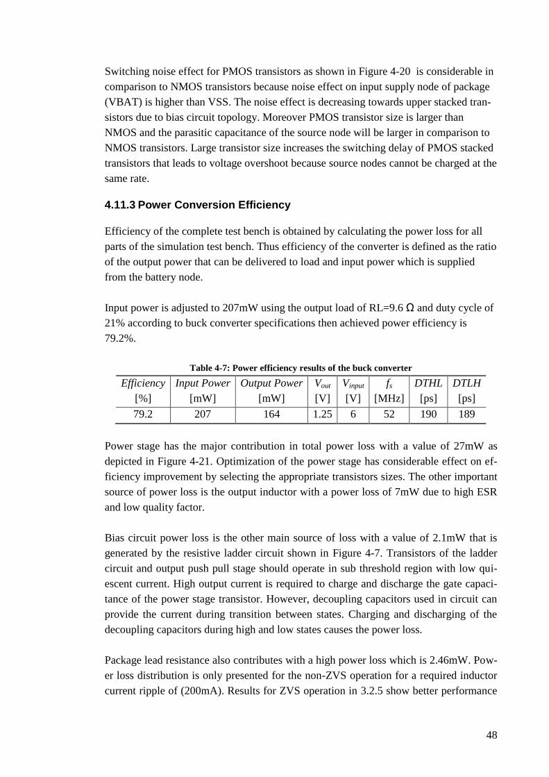
Chapter 5 Buck Converter with Variable Battery Supply ............................................. 50
5.1 Proposed Circuit ........................................................................................... 50 5.2 Simulation Results........................................................................................ 54
Chapter 6 Conclusions ................................................................................................... 56
References ....................................................................................................................... 58
Appendix-1: .................................................................................................................... 60
Page 6
VI
ABBREVIATIONS
DC-DC Direct-Current to Direct-Current
CMOS Complementary Metal Oxide Semiconductor
MOS Metal-Oxide-Semiconductor
LDMOS Lateral Diffused Metal-Oxide-Semiconductor
IC Integrated Circuit
PWM Pulse Width Modulation
DTLH Dead Time at Low-to-High transition
DTHL Dead Time at High-to-Low transition
ZVS Zero Voltage Switching
NMOS N-type Metal Oxide Semiconductor
PMOS P-type Metal Oxide Semiconductor
PCB Printed Circuit Board
SoC System-on-Chip
PMU Power Management Unit
LDO Low Drop Out Regulator
PMIC Power Management Integrated Circuit
Page 7
1
CHAPTER 1
Introduction
Significant growth in portable device market has been a driving force in design and im-
plementation of more complex and power efficient building blocks such as processors,
memory chips and RF front ends. This growing trend goes along with higher levels of
integration and increased total power consumption. Therefore, design of improved pow-
er management units (PMUs) becomes more important. Lithium-Ion battery is the most
widely used power supply source for these portable devices and it is characterized with
a variable voltage range between 2.8-to-5.5V depending on the state of the charge [1].
For this reason PMUs are necessary to provide a stable supply voltage for different inte-
grated blocks within the portable device.
Figure 1-1 illustrates a typical PMU architecture for System-on-Chip design. PMU inte-
grates several high efficiency DC-DC converters and Low-Drop-Out regulators (LDOs)
for different blocks such as processor core, I/O and RF transceiver.
Figure 1-1: Power management unit for SoC design.
DC-DC
Buck
DC-DC
Buck/Boost
DC-DC Prog.
Buck
Inductor less
DC-DC
(Switched capacitor)
Battery
LDO
(Low Quiescent)
Capacitor less
LDO
+
-
Programable
LDO
LDO
DSP Core
LCD Backlight
1.2V
5V
Processor1.2V
RTC1.2V
Memory, I/O1.8-2.5V
Low Noise
RF Block
3.3V
Page 8
2
1.1 Motivation
Integration of Power Management Integrated Circuits (PMICs) with baseband processor
and RF modules using advanced CMOS technology provides power delivery with high-
er efficiency. The higher power efficiency is achieved by integration of the PMU (Buck
DC-DC Converters) on the same chip with digital logic circuits in an advanced System-
on-Chip design and by elimination of extra IC package and PCB connections.
Advanced CMOS technology is one of the best candidates for implementation of inte-
grated PMUs because of its mature processing and lower cost through mass production.
Monolithic integration of buck converters in CMOS requires small silicon area. This
can be achieved by increasing the switching frequency to reduce the filter component
size and also output voltage ripple. At the same time the higher switching frequency
affects the dynamic loss and power efficiency. Advanced CMOS technology such as
45nm CMOS can be used for high switching frequency application due to its low supply
voltage that decreases the dynamic power loss. Another benefit of 45nm CMOS is the
lower on-resistance because of the smaller channel length.
The low breakdown voltage and high leakage current are the main drawbacks of CMOS
technologies. Lateral diffused MOS (LDMOS) transistors can be used as an alternative.
The LDMOS transistor can operate with higher supply voltage. However, high on-
resistance and extra processing is required to integrate these devices with core transis-
tors and this is the limiting factor for SoC implementation. Another method is to use
cascode transistor structure as the solution to keep the supply voltage of the power stage
transistor within the breakdown voltage limit. This technique is employed in circuits
such as DC-DC converters and power amplifiers operating with an input voltage higher
than the breakdown voltage. Bias circuit is the main design challenge for these circuits
specially, when more than two transistors are used in the stack. The bias circuit should
generate the bias voltage required for switching operation of power stage transistors by
considering the appropriate timing in order to ensure the circuit reliability.
1.2 Outline
This thesis studies the design of a high frequency integrated buck converter with main
focus on power stage circuit. The supply voltage for the first design is considered to be
fixed at a battery voltage level of 6V. For the second design, the supply voltage varies
from 3.5V-to-6V. Chapter 2 starts with studying the main DC-DC converter architec-
tures. Then, challenges regarding the use of low voltage CMOS technology are intro-
duced and finally cascode structure is studied as an efficient and cost effective way to
overcome the breakdown condition. Chapter 3 is dedicated to design of power stage and
simulation results to investigate the circuit operation and reliability issues concerning
Gate-Oxide and hot carrier effects. Chapter 4 studies the design of main blocks for buck
converter and obtained simulation results for each block. The achieved converter per-
Page 9
3
formance is investigated by including the dominant parasitic effects in the simulation
test bench. Chapter 5 presents design and simulation results of a buck converter with a
variable input battery voltage from 3.5V to 6V. Dynamic operation is achieved by using
a novel biasing circuit that operates in different regions for 3.5V<VBAT<4.5V and
4.5V<VBAT<6V. The biasing circuit ensures a reliable operation of all the transistors
with respect to a maximum breakdown voltage of 1.8V in 45nm CMOS. Chapter 6 con-
cludes the thesis with main achievements.
Page 10
4
CHAPTER 2
Background Theory
In this chapter first we summarize different types of DC-DC converters, their main fea-
tures and comparison between them. Non-idealities of low voltage CMOS technologies
with main focus on gate-oxide breakdown and hot carrier effect are presented in the
second part. Last part explains the cascode structure operation by representing the volt-
age distribution across stacked transistors. DC-DC voltage converters are classified to
linear voltage regulators and switched mode converters based on conversion mecha-
nism. Each converter type is characterized with specifications that are required for cer-
tain applications. The main important converter parameters are power efficiency, volt-
age conversion ratio, maximum output power and number of the components that speci-
fies the power loss and efficiency.
2.1 Linear Voltage Regulator
Linear voltage regulator in the simplest structure that consists of two resistors as the
voltage divider as shown in the schematic diagram of Figure 2-1. This type of convertor
suffers from high power loss and low efficiency. The error amplifier subtracts the feed-
back output voltage from the reference voltage. The analog buffer with low output im-
pedance is used for driving the gate of output transistor. In this topology same feedback
loop is used for tracking the output voltage and responding to a variable load [2]. This
type of the converter does not need to use bulky components like on-chip capacitor and
inductors and therefore it is one of the best candidates as a DC-DC converter in power
management units (PMUs) and System-on-Chip (SoC) applications. The other ad-
vantage is higher power supply rejection ratio (PSRR) in comparison to switch-mode
DC-DC converters with noise effect that is generated by filter components.
Figure 2-1: Conventional linear voltage regulator circuit [2].
Analog
Buffer
Error
Amplifier
+
-Vref
Output
Device
Vin
Load
Vout
Page 11
5
Efficiency of linear regulator can be estimated as the ratio of output and input voltages
therefore, in order to attain higher efficiency the voltage aspect ratio should be small.
Low dropout regulator (LDO) can fulfill this design requirement. Large output capaci-
tance is used at the output stage to achieve better noise suppression that is a main con-
straint [3].
2.2 Switched Mode Converter
Switched mode converters employ energy storing passive components and also switches
to change the connection path. This type of converters are categorized as inductive DC-
DC and switched capacitor or charge pump DC-DC converters. This section studies the
basics of switched mode converters with main focus on inductive step-down converters.
Switched capacitor DC-DC converter:
Switched capacitor converter operation is based on charging the capacitors in one phase
and then delivering the charge to the output capacitor in second phase. The charging
process of the capacitors intrinsically consumes the power even if we consider the
switches as lossless components. Basic operation of the converter is shown in Figure
2-2.
Figure 2-2: Ideal series-parallel step-down switched capacitor DC-DC converter [4].
In phase one ( 1 ) flying capacitor (C1) and output capacitor 2( )C will be charged and
during phase two ( 2 ) both capacitors are parallel and 1C starts charging the output
capacitor. From (2.1) we can conclude that for the ideal state, output voltage is ap-
proaching to a maximum voltage value of ( / 2inV ) for 100% efficiency [4].
1 1 1
1
1
( 2 )
1 2
out L out L SW SW L SW C L sw in out
L SW inout
L SW
V R I R f Q R f C V R f C V V
R f C VV
R f C
(2.1)
In ideal state by considering the high switching frequency, output voltage is independ-
ent from the load therefore voltage ripple is very small [4]. The advantage of using this
Page 12
6
type of converter is the ability for monolithic integration with high efficiency and the
drawback is the limited voltage ratio with maximum value of 0.5. Moreover output ca-
pacitor size limits the output current. Therefore, attained output power density is less
than inductive DC-DC converters [5].
Inductive DC-DC converter:
Inductive DC-DC converters are classified to step-up, step-down and step up/down con-
verters. This type of the converter uses both inductors and capacitors as energy storage
components. Therefore, more silicon area is required for a monolithic integration com-
pared to previous types. However, this converter can provide high efficiency and high
power density which makes it as the best candidate for SoC design.
Buck converter suffers from switching noise effect at the output node due to low reso-
nance frequency of the filter components. This parasitic effect is more significant for
higher load currents since the parasitic inductors of the PCB traces increase the noise
effect. Thus proper design of the PCB layout is essential for this type of converter and it
can decrease the noise effect.
As demonstrated in Figure 1-1 step down converters are used at first stage to convert the
battery voltage to a lower level that is suitable for conversion using LDOs. The main
features of the studied DC-DC converters are summarized in Table 2-1.
Table 2-1: Comparison between different types of DC-DC converters [16].
Design Parameters Linear Regulator Charge-pump Inductive type
Voltage Conversion Mode Step down Step-up &
Step-down
Step-up & Step-
down
Efficiency Low High High
Maximum Output Current High Low High
Design Complexity Simple Complicated Complicated
Silicon Area Small Small Big
2.3 Buck DC-DC converter
Buck converter operates as a step-down voltage converter that generates an output volt-
age which has a lower level than the input voltage. Circuit model of the buck converter
is shown in Figure 2-3 (a). Circuit operation is based on two switching phases, in the
first phase SW1 is closed and Vx node starts charging to a voltage value of Vin. In the
Page 13
7
second phase SW2 is closed and SW1 is open therefore Vx will be discharged to 0V.
Generated Vx signal is a rectangular pulse as given in Figure 2-4 (a). A second order
output filter is employed to obtain the average of the Vx signal [4].
Considering ideal filter components and also a rectangular Vx pulse, the output voltage
of the converter is given as:
out inV DV (2.2)
The inductor current ripple can be obtained according to the voltage of the inductor and
the output voltage as shown in equation (2.3). Decreasing the inductor value increases
the inductor current ripple [6]. Figure 2-4 (c) shows the inductor current and also the
output current which is the average of the inductor current.
(1 ) (1 )in out
L
S S
V D D V DI
Lf Lf
(2.3)
Output voltage ripple can be defined as following [6]:
2
(1 )1 1
2 2 2 8 8
S OL L
sw sw
T V DI IQV
C C LCf LCf
(2.4)
Equation (2.2) shows that buck converter can generate a wide output voltage range by
changing the duty cycle of the driver signals. Voltage ripple affects the output node as
shown in Figure 2-4 (b). To decrease the output voltage ripple switching frequency
should be increased as given in equation (2.4) however this will also increase the
switching and gate drive losses specifically for a higher load current.
Figure 2-3: Synchronous buck converter (a) Circuit model; (b) Power stage [7].
Figure 2-3 (b) shows the schematic circuit diagram of a buck converter using power
stage that operates as the switch. P-Drive and N-Drive signals control the switching
operation of the power stage transistors (Mp1 and Mn1), gate-source and gate-drain
voltages are biased with maximum allowed voltage of VDD to achieve the minimum
possible on-resistance thus smaller transistor width can be selected. The smaller transis-
tor width helps to decrease switching loss.
Vin=VDD
Cf
Lf
P-Drive
N-Drive
Vout
Cf
Lf
RL Vin
VX Vout
(a) (b)
SW1
SW2
VX
iLiout
MP1
Mn1
V2 = VDD
V1 = 0
V2 = VDD
V1 = 0
Page 14
8
Figure 2-4: Steady state waveforms of the converter in continuous conduction mode (CCM) (a) Vx ,
(b) Vout and (c) Iout [7].
2.3.1 Cascode power stage for input voltage up to 2VDD
For an input voltage higher than the gate-oxide breakdown cascode structure is pro-
posed. By using two stacked transistors in power stage, the input voltage can be in-
creased to a maximum voltage of 2VDD.
Vin=2VDD
Cf
Lf Vout
(c)
P-Drive
N-Drive
VDD
RL
VX
iL
iout
MP1
MP2
Mn2
Mn1
V2 = 2VDD
V1 = VDD
V2 = VDD
V1 = 0
Figure 2-5: Cascode power stage with input voltage of 2VDD.
In the circuit shown in Figure 2-5, gate-oxide voltage across each transistor of the stack
is considered to be VDD. However voltage distribution of the power stage transistors is
changed according to the number of transistors as demonstrated in equations (2.6) and
(2.7). From Figure 2-5, N-Drive signal controls the switching operation of Mn1 and
Mn2. Level shifter circuit is required to shift up the signal of N-Drive by 1V to generate
the P-drive signal that controls the switching of Mp1 and MP2.
Vout
Iout
t
t0
0
Vx(t)
iL(t)
∆iL
D/fs
1/fs
Vin
Vout
t0
Vout(t)
∆Vout
(a)
(b)
(c)
Page 15
9
2.3.2 Cascode power stage for input voltage up to 3VDD
For the input voltage of 3VDD, three stacked transistors are used in the power stage.
Therefore, a bias circuit is required to generate the gate bias voltage with specific timing
for on/off states. Two architectures are proposed, the first circuit architecture is based
on using multiple level shifter sachem and the second circuit uses the external bias cir-
cuit for biasing the transistors gate. Power stage in Figure 2-6 requires using the high
speed level shifter circuit to decrease the switching delay that can affect the charging
and discharging rate of the source nodes and then voltage overshoot of VDS and VGS
signals. Without considering the appropriate timing there will be possibility for gate-
oxide breakdown and hot carrier degradation effect. Power stage circuit in Figure 2-7
does not need additional level shifter circuit to generate the gate bias voltage for com-
mon gate connection. Therefore, the only factor that determines the switching time will
be the size of the power stage transistor.
Figure 2-6: Three cascode stage biased with two level shifter circuits.
Figure 2-7: Three cascode stage with synchronized gate biasing.
V1 = 1V
V2 = 0V
N-Drive
VDD
2VDD
2V, Level shifter
1V, Level shifter
3VDD
3VDD3VDD3VDD 2VDD
2VDD VDD
To output
Filter VX
Mn1
Mn2
Mn3
Mp3
Mp2
Mp1
N-Drive
3VDD
3VDD3VDD
2VDD
VDD
2V, Level shifter
3VDD 2VDD
To output
FilterVX
Mp3
Mp2
Mp1
Mn1
Mn2
Mn3
Mpb1
Mnb1
V1 = 1V
V2 = 0V
Page 16
10
2.3.3 Cascode power stage for input voltage up to 4VDD
Power stage with four cascode transistors requires using three level shifters and a bias-
ing circuit that generates the common gate bias voltage for Mpb4 and Mnb4 as depicted
in Figure 2-8.
Figure 2-8 : Four cascode stage biased with three level shifter circuits.
Figure 2-9: Four cascode stage with synchronized gate biasing.
Design principle of the bias circuit in Figure 2-9 is the same with the three cascode
power stage shown in Figure 2-7 nevertheless additional bias circuit that generates the
4VDD
To output
Filter VX
Mn2
Mn3
Mn4
Mp4
Mp3
Mp2
Mn1
Mp1
4VDD4VDD
2V, Level shifter
3VDD 2VDD3VDD
1V, Level shifter
4VDD 3VDD
V1 = VDD
V2 = 0V
N-Drive
2VDD
VDD
1V, Level shifter
2VDD VDD
Mpb1
Mpb2
Mnb1
Mnb2
4VDD
N1G
N2G
N3G
N2S
N3S
N4S
P3G
P2G
P1G
P4S
P3S
P2S
Mn1
Mn2
Mn3
Mn4
Mp4
Mp3
Mp2
Mp1
3VDD
VDD
To Output
Filter2VDD
4VDD4VDD
VX
V1 = VDD
V2 = 0V
N-Drive
Mnb1
Mnb2
Mpb3
Mpb2
Mpb1
Mnb3
C1
C2
C3
C4
Page 17
11
off state voltage is used to bias the transistors including P3 and N3. Bias circuit opera-
tion with more details including six stacked transistors is explained in Chapter 3.
2.4 Design in Nano-Scale CMOS
Recent developments in integrated circuit technologies facilitate the use of novel silicon
technologies in order to fulfill different design requirements regarding speed, complexi-
ty, better integration and higher power efficiency. The main challenge with respect to
using the nanometer CMOS technology is the lower gate-oxide and PN-junction break-
down voltages duo to shrinking the gate length and also Gate-Oxide thickness. Cascode
design is the technique that can be used to limit the voltage across transistor terminals
for a more reliable performance.
2.4.1 Reliability Issues
In order to maintain the constant lateral and vertical electric fields three main parame-
ters that should be scaled with the same factor are dimensions, supply voltage and dop-
ing level. For the nano-scale process nominal voltage cannot be scaled the same as
physical dimensions. The other parameter is the threshold voltage that cannot be de-
creased further, since this voltage value controls the switch off condition. The major
reliability issues concerning nano-scale CMOS technologies are Time Dependent Die-
lectric Breakdown (TDDB), Hot Carrier degradation (HCD) and Electromigration effect
as explained below.
Time dependent dielectric breakdown (TDDB):
Time dependent breakdown can be translated as the gate-oxide breakdown failure rate
so that lower TDDB means higher failure rate. The wear out of the insulating properties
of silicon-oxide in the gate result in the formation of conducting path through the oxide
to substrate. As technology is scaled down the gate-oxide thickness has been scaled as
well. This scaling causes a large electric field in the gate-oxide junction which can gen-
erate a tunneling current. The oxide life time will be affected by this tunneling current
and the flow of charges through the oxide layer [8].
Hot carrier degradation (HCD):
When electrons in transistor channel are given enough energy and became ”hot” they
may collide with other substrate atoms and create electron and hole pairs which also
leads to collision with other substrate atoms this phenomena so-called impact ionization
causes high substrate current, device breakdown and silicon to gate-oxide degradation.
When the voltage across the transistor is scaled with the same dimensional scaling fac-
tor, electric field remains almost constant and the probability of ionization will be de-
creased however for nanometer CMOS technology the effective channel length is de-
Page 18
12
creasing faster than the supply voltage and therefore, increased electric field that in-
creases the possibility of ionization impact [9].
Electromigration:
High current flowing through the metal lines may cause metal ions to be transported
through the interconnection of metal layers. This physical migration of material from a
certain location to another location creates open circuit or voids on locations where ma-
terial is removed and hillocks on locations where extra material is added. Electromigra-
tion can damage metal layers and eventually result in circuit failure [8].
2.4.2 Breakdown Mechanisim
Reliability issues explained in previous part leads to long term degradation of the tran-
sistor. When the voltage across the transistor terminals exceeds from a specific break-
down limit, there will be a instantaneous breakdown. Breakdown mechanism is catego-
rized into junction breakdown and gate oxide breakdown.
Gate oxide breakdown:
The effect of gate oxide breakdown on Nano-Scale CMOS circuits expressed as the
failure condition that can happen by applying the gate-oxide junction (gate-drain, gate-
source) voltage more than maximum allowable voltage. Break down condition leads to
hot carrier effect and then oxide degradation. Breakdown voltage depends on the oxide
thickness and by scaling the oxide thickness breakdown voltage will be decreased. The
circuit design approach is biasing the gate-source voltage in such a way that limits the
gate-source voltage to a maximum voltage of 1V. Since the breakdown voltage of 45nm
generic CMOS process is 1.1V, this will guarantee the reliable circuit operation.
Junction breakdown:
By increasing the reversed biased voltage of P-N junction, lateral electric field will be
increased and the high reversed current can generate an avalanche breakdown. Simula-
tion results for the breakdown voltage of drain-bulk junction for 45nm CMOS is shown
in Figure 2-10.
Page 19
13
7.75V
7.3V
P-N junction
break down
2.8mA
6.58nA36mA
7.75V
7.3V
P-N junction
break down
2.8mA
6.58nA36mA
Figure 2-10: Junction breakdown voltage (VDB) for 45nm CMOS. (a) NMOS; (b) PMOS
Impact ionization rate is infinite by increasing the Drain-Bulk voltage above the break-
down voltage and avalanche multiplication will result in high reversed bias current as
shown in Figure 2-10 (a)-(b).
2.4.3 Cascode Circuit Architecture
There are different techniques to increase the breakdown voltage by using different
structures such as Laterally Diffused MOS transistors (LDMOS) or modification of the
CMOS process by using thicker oxide. Integration of LDMOS with the mainstream na-
nometer process needs extra processing; high on-resistance is the other drawback that
affects the efficiency and chip size.
In some applications like switching converters, power amplifiers and LNA with high
input supply voltage to overcome the circuit reliability issues regarding breakdown
voltage cascode topology can be used as a cost effective solution. The principle of
18.8V
18.2V
PN junction
break down
0 ≤ Vgs ≤ 0.55V
7.4nA 4mA473uA
100mA
18.8V
18.2V
PN junction
break down
0 ≤ Vgs ≤ 0.55V
7.4nA 4mA473uA
100mA
(a)
(b)
Page 20
14
cascode topology using three stacked transistors is depicted in Figure 2-11 (c). The
maximum voltage across each transistor terminals is equal to the nominal supply volt-
age for a gate-oxide junction (VDD) as shown in Figure 2-11 (a).
VDD
VDD
VDD
VDD
VDD
3VDD
(a) (c)
S
B
VDD
VDD
B
VDD
B
VDD
VDD
VDD
VDD
D
GB
VDD
D
G
G
VDD
VDD
(b)
B
VDD
VDD
B
G
D
VDD
VDD
2VDD
Figure 2-11: Scheme of stacking transistors with triple-well CMOS.
For triple well process, transistor bulk can be connected to the source therefore for all
stacked transistors we have VGS=VGB and VDS=VDB. Therefore, voltage across gate-bulk
and drain-bulk is limited to VDD. Number of the stacks depends on the junction voltage
of N-well and p-substrate. Stacking of transistors should provide an equal voltage dis-
tribution across transistor terminals however as will be explained later each transistor in
stack will experience different supply voltage across the nodes.
Biasing and voltage stress condition
Critical voltages are studied for two cases when transistors are on and off. In off state,
Gate-Source voltage condition is: VGS= Vth. However, in sub-threshold region because
of leakage current, parasitic capacitance of the source node can still be charged thus
Gate-Source voltage value is in the range of 0 ≤ VGS ≤ VTH. In on state, Drain-Source
voltage for each transistor is equal to VDS=Ron×ID. On-resistance value depends on tran-
sistor size and Gate-Source voltage as given below:
1
( )ON
ox GS TH DS
RW
c V V VL
(2.5)
The minimum on-resistance from equation (2.5) is obtained for the maximum allowed
Gate-Source voltage (VDD). For all the transistors in the stack, we will assume that
VGS=VDD.
Page 21
15
Figure 2-12 Voltage distribution (a) On state; (b) Off state.
Cascode stage with three stacked transistors supplied with a fixed voltage value of
3VDD is shown in Figure 2-10. VGS and VGD values are the critical voltages that need to
satisfy the breakdown condition limits. Therefore, in on-state all transistors should be
biased with following condition: VGS=VDD, VGD ≤ VDD. When all transistors are
switched off the only required condition is VGD ≤ VDD. Voltage distributions for cas-
code stage in on and off states are depicted in Figure 2-12. Output voltage is equal to:
1 2 3 3out DS DS DSV V V V VDD . However, VDS1, VDS2 and VDS3 according to equation
(2.7) are not equal for stacked transistors. Gate-Drain voltages have also different values
rather than VDD as given in equation (2.7) for on-state.
I. On state
1 1 1 1 1
2 1 2 1 2
3 1 2 3 1 2 3
( )
( ) ( )
GS GD GS DS DS
GS DS GD DS DS
GS DS DS GD DS DS DS
V VDD V V V VDD V
V VDD V V VDD V V
V VDD V V V VDD V V V
(2.6)
II. Off state
3 3 3 3 3
2 2 2 3 2 3 2
1 1 1 2 3 2 1 2
( )
( ) 3
GD DS GS GD GS
GD G D GS DS GS GS
GD G D DS DS GS DS GS
V VDD V V V VDD V
V V V V VDD V VDD V V
V V V V V VDD V VDD V VDD V
(2.7)
B
0V
B
VGD3
B
VGS3
VDS3VG3=2VDD
VG2=VDD
VIN=0V
VDS2
VGD2
VGS2
VDS1
0
VGD1
VOUT=3VDD
B
VDD
B
VGD3
B
VGS3
VDS3VG3=VDD
VG2=VDD
VIN=VDD
VDS2
VGD2
VGS2
VDS1
VOUT
VGD1
0
(a) (b)
Page 22
16
2.5 Literature Survey
Previous works published in references are classified with respect to the output stage
architecture. Reference [10] presents the buck converter with variable supply voltage in
the range of 2.8-4.2V, Output stage architecture is based on 45nm CMOS with break-
down voltage of 1.8V therefore three PMOS stacked transistors are used in power stage.
Since two stacked NMOS transistors can be used in one well process then LDMOS type
transistor is used in power stage. 1.8V SC converter with three reconfigurable setting is
directly connected to the battery and stacking regulators are used to generate the dynam-
ic reference voltages. Reference [11] represents the ultra-low quiescent current digitally
controlled buck converter that employs PWM method for high load and PFM control
method in light mode to achieve the highest efficiency. Ring-ADC is proposed due to
robustness to switching noise. Power stages consist of two stacked transistors and inter-
nal voltage regulators that are used to generate the gate bias. Reference [12] employs
the adaptive gate biasing method to achieve lower on resistance, small chip size and
high efficiency of 94%. Decoupling capacitors are realized by using the transistors to
prevent the voltage overshoot. In Reference [13], digitally controlled converter is pro-
posed. PFM is used for start-up and standby operation and PWM for normal operation.
DeMOS transistors of the power stage are built in single-gate-oxide form and biased
with a voltage of Vcore =1V.
Table 2-2: Comparison between different types of buck converters in the literature
Output
Stage Cascode DeMOS
Ref [10] [11] [12] [13]
Technology 45nm
CMOS
0.250um
CMOS
0.350μm
CMOS
28nm
CMOS
Vin [V] 2.8-4.2V 5.5-2.8 2.5-5 2.4-5.5
Vout [V] 0.6-1.2V 1-1.8 1-4 0.9-1.8
fs [MHz]
PWM:2MHZ
PFM:1.5MHz
SC:4MHz
PWM:0.5-
1.5MHz
PFM:600KHz
1.3
DPWM:1.6MHz
L [uH] 10 10 4.7 3.3
C [uF] 2 47 4.7 22
Iout [A] NA Max 0.4 100uA-0.4
Max 0.5
η(Peak)
87.4% 92% 94% 90% [%]
Page 23
17
CHAPTER 3
Cascode Power Stage
In this chapter design and simulation results of a cascode power stage for a DC-DC
buck converter is presented. The input voltage of the power stage is considered to be 6V
which requires stacking of six transistors with a maximum supply voltage of 1V across
each transistor terminals. In order to ensure reliable operation regarding gate-oxide
breakdown, gate nodes of the transistors are required to be biased with certain voltage
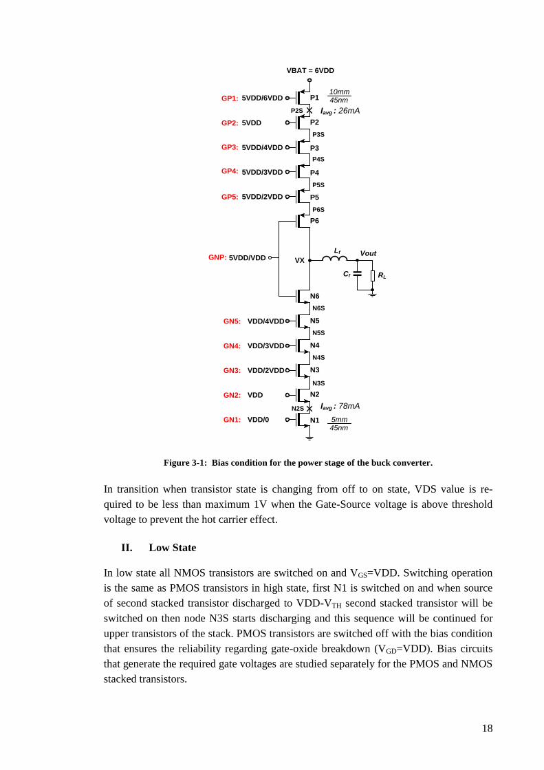
values in the on and off states as illustrated in Figure 3-1.
3.1 Design Procedure
Cascode power stage of the DC-DC converter with input voltage of 6V requires driving
gate voltages that are categorized in two states, when output voltage (VX) is high and
pull-up PMOS transistors are switched on and when the output voltage is low and all
pull-down NMOS transistors are switched on. Reliability of the circuit depends on the
voltage stress condition across Gate-Drain and Gate-Source junctions; thus bias circuit
should generate the Gate-Source and Gate-Drain voltages with a maximum voltage of
1V. Minimum possible on-resistance is an important factor to achieve higher efficiency.
For this reason, Gate-Source is biased with a maximum voltage of 1V to achieve the
minimum on-resistance as given in equation (2.5) [14]. Circuit operation and design
requirements are studied in two cases for the high and low states.
I. High State
In high state VX node voltage is pulled up and all PMOS transistors are switched on
then Source-Gate voltage across each PMOS transistor is VDD=1V, this requires all
gates to be biased with 5VDD. Drain-Source voltage of each transistor depends on the
on-resistance and drain current which is changing by the inductor current. In this case
NMOS transistors are switched off. Regarding gate-oxide breakdown VGD is required
to be maximum 1V.
Since the Gate-Source voltage for each NMOS transistor in off state is in the range of
0 ≤ VGS ≤ VTH then according to equation (2.7) Drain-Source voltages is not equally
distributed between NMOS transistors, the value depends on the Gate-Source voltages
of stacked transistors as explained before.
Page 24
18
Figure 3-1: Bias condition for the power stage of the buck converter.
In transition when transistor state is changing from off to on state, VDS value is re-
quired to be less than maximum 1V when the Gate-Source voltage is above threshold
voltage to prevent the hot carrier effect.
II. Low State
In low state all NMOS transistors are switched on and VGS=VDD. Switching operation
is the same as PMOS transistors in high state, first N1 is switched on and when source
of second stacked transistor discharged to VDD-VTH second stacked transistor will be
switched on then node N3S starts discharging and this sequence will be continued for
upper transistors of the stack. PMOS transistors are switched off with the bias condition
that ensures the reliability regarding gate-oxide breakdown (VGD=VDD). Bias circuits
that generate the required gate voltages are studied separately for the PMOS and NMOS
stacked transistors.
VBAT = 6VDD
N2S
N3S
N4S
N5S
N6S
5VDD/6VDD
P6S
P5S
P4S
P3S
P2S
N1
N2
N3
N4
N5
N6
P6
P5
P4
P3
P2
VX
P1
5VDD
5VDD/3VDD
5VDD/4VDD
5VDD/2VDD
VDD/4VDD
VDD/3VDD
VDD/2VDD
VDD
VDD/0
5VDD/VDDLf
RL
Vout
Cf
GP1:
GP2:
GP3:
GP4:
GP5:
GNP:
GN5:
GN4:
GN3:
GN2:
GN1:
Iavg : 26mA
10mm45nm
5mm45nm
Iavg : 78mA
Page 25
19
3.1.1 Bias circuit for PMOS Power Transistors
Biasing of P1 is accomplished by employing a level shifter which shifts up the signal
level by 5VDD. P2 is biased with a fixed voltage of 5VDD as shown in Figure 3-1. Bias
circuit design for other transistors is based on cascode structure and the number of re-
quired stack transistors depends on the voltage difference between the on and off states.
Figure 3-2: Bias circuit for the stacked PMOS transistors.
Bias circuit for each transistor of the stack is depicted in Figure 3-2. In on state all gate
nodes are biased with 5VDD since NMOS transistors including Mnb1, Mnb2, and
Mnb3 need to be switched on. Source nodes of PMOS transistors cannot be charged at
the same time because switching sequence starts with P1 in Figure 3-1 for GP1=5VDD.
After P2S is charged to 5VDD+VTH, P2 will be switched on, same operation is happen-
ing for P3, when source is charged to 4VDD+VTH transistor is switched on and after it is
charged to 6VDD as shown in Figure 3-2 (d) GP3 will be charged to 5VDD because
Mbn1 is supplied with reference voltage of 5VDD, in this case gate-source voltage for
Mbn1 is VDD. Similarly for other biasing transistors (Mbn2, Mbn3 and Mbn4), first
P4S, P5S and P6S are charged to 6VDD and then GP4, GP5 and GNP are biased with
5VDD.
In the off state, for PMOS stacked transistors first P1 will be switched off and then bias-
ing condition of other transistors will depend on high-to-low dead time according to
switching operation depicted in Figure 3-12 and Figure 3-13. As shown in Figure 3-2
(a) gate voltage of GNP depends on source voltage of NMOS and PMOS transistors.
Thus, during the dead time inductor current starts discharging the source nodes which
5VDD
6VDD/4VDD
6VDD/3VDD
6VDD/2VDD
6VDD/VDD
VDD
GP3
GP4
GP5
P3S:
P4S:
P5S:
P6S:
GNP
0/5VDD
0/4VDD
0/3VDD
0/2VDD
N6S:
N5S:
N4S:
N3S:
GN5
GN4
GN3
2VDD
GNP
GN5
GN4
3VDD
GP5
4VDD/2VDD
GP4
4VDD
5VDD
P3S
P4S
P5S
GP5
P3S
P4S
GP4
5VDD
P3S
5VDD
(a) (b)
Mnb1
Mpb5
Mnb1
Mnb2
Mpb6
Mpb7
Mnb1
Mnb2
Mnb3
Mnb1
Mnb2
Mnb3
Mnb4
Mpb2
Mpb1
Mpb3
Mpb4Mpb8
Mpb9
Mpb10
GP3
(c) (d)
Page 26
20
simultaneously discharges the GNP and other gates. Therefore, gate nodes will be dis-
charged to lower voltage levels even if N-Drive=0V as illustrated in Figure 3-13 for
ZVS operation, however discharging of the PMOS gate voltages will be accelerated
when NMOS stage is switched on.
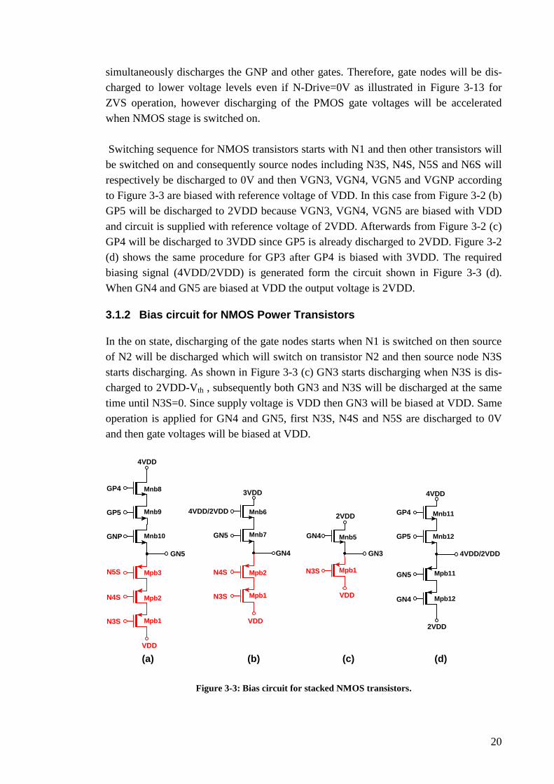
Switching sequence for NMOS transistors starts with N1 and then other transistors will
be switched on and consequently source nodes including N3S, N4S, N5S and N6S will
respectively be discharged to 0V and then VGN3, VGN4, VGN5 and VGNP according
to Figure 3-3 are biased with reference voltage of VDD. In this case from Figure 3-2 (b)
GP5 will be discharged to 2VDD because VGN3, VGN4, VGN5 are biased with VDD
and circuit is supplied with reference voltage of 2VDD. Afterwards from Figure 3-2 (c)
GP4 will be discharged to 3VDD since GP5 is already discharged to 2VDD. Figure 3-2
(d) shows the same procedure for GP3 after GP4 is biased with 3VDD. The required
biasing signal (4VDD/2VDD) is generated form the circuit shown in Figure 3-3 (d).
When GN4 and GN5 are biased at VDD the output voltage is 2VDD.
3.1.2 Bias circuit for NMOS Power Transistors
In the on state, discharging of the gate nodes starts when N1 is switched on then source
of N2 will be discharged which will switch on transistor N2 and then source node N3S
starts discharging. As shown in Figure 3-3 (c) GN3 starts discharging when N3S is dis-
charged to 2VDD-Vth , subsequently both GN3 and N3S will be discharged at the same
time until N3S=0. Since supply voltage is VDD then GN3 will be biased at VDD. Same
operation is applied for GN4 and GN5, first N3S, N4S and N5S are discharged to 0V
and then gate voltages will be biased at VDD.
Figure 3-3: Bias circuit for stacked NMOS transistors.
VDD
N5S
N4S
N3S
GN5
GP4
GP5
GNP
4VDD
VDD
N4S
N3S
GN5
4VDD/2VDD
GN4
3VDD
VDD
N3S
GN4
GN3
2VDD
Mnb5
Mnb6
Mnb7
Mnb8
Mnb9
Mnb10
Mpb1Mpb2
Mpb1Mpb2
Mpb1
Mpb3
(a) (b) (c)
GP5
GP4
4VDD
Mnb11
Mnb12
4VDD/2VDD
2VDD
GN5
GN4
Mpb11
Mpb12
(d)
Page 27
21
In the off state, first N1 is switched off then N2S will be charged to VDD-Vth and N2
will be switched off, similarly N3S, N4S, N5S and N6S will start charging nevertheless
continuation of charging depends on low-to-high dead time because as shown in Figure
3-3 (a) GN5 will start charging when GNP voltage is above VDD+Vth. When P1 is
switched on, consecutive charging of gate nodes, as explained in Section 3.1.1, will bias
PMOS transistors with 5VDD. According to Figure 3-3 (a) GN5 starts charging to
4VDD and when GN5 is charged to VDD+Vth, Mnb7 will be switched on and subse-
quently GN4 will start charging to 3VDD according to Figure 3-3 (b). In a similar way
GN3 will be biased with 2VDD when Mnb5 is switched on as shown in Figure 3-3 (c)
and circuit (d) generates the required bias voltages in Figure 3-3 (b), when GP5 and
GP4 are biased with 5VDD and the output voltage is 4VDD.
3.1.3 Decoupling Capacitors
Coupling effect of the large gate-drain capacitance in transition from on to off states
makes the large voltage overshoot on transistor gate nodes. Therefore, decoupling ca-
pacitors are used to suppress the coupling effect by bypassing the current from the gate
node to a lower voltage that is specified as the reference voltage.
Figure 3-4 (a) and (b) show the bias circuit for P4 and P3 stacked transistors in power
stage. Figure 3-4 (c) and (d) are the simplified electrical models of the transistors ac-
cording to switching operation.
Figure 3-4: Bias circuit operation with decoupling capacitors.
Decoupling capacitors are calculated based on two conditions. First by considering that
charging and discharging of the capacitors including decoupling capacitor and parasitic
capacitance should be at the same rate then from Figure 3-4 (d) we have 1 2on onR R .
According to Figure 3-4 (c) and (d) charging and discharging time constant are 22 onR C
and 1onR C respectively. Consequently to assure same charge and discharge rates for SP3
3VDD
GP5
4VDD/2VDD
GP4
4VDD
P3S
P4S
GP4
5VDD
P3S
5VDD
(a) (b)
Mnb1
Mpb5
Mnb1
Mnb2
Mpb6
Mpb7
5VDD
C2 C1
GP3
5VDD
Ron1
C1
GP3
5VDDRon2
4VDD
5VDD
2Ron1
C2
GP4
5VDD2Ron2
3VDD
5VDD
(c) (d)
Page 28
22
and SP4 we need to have RonC1=2RonC2 and capacitors value are determined as:
1 2 1 2 1 22 2on on on onR R R C R C C C
Total parasitic capacitance of the transistors has a small value and it is in parallel with
decoupling capacitors so the effect of parasitic capacitance is neglected.
Same principle is used for GP5 and GNP from Figure 3-2 to obtain decoupling capacitor
values. Decoupling capacitor values are 3 2 1 4 3 1
2 1 3 1 and
3 3 4 4C C C C C C .
Calculation of decoupling capacitors for NMOS stacked transistors obeys the same rule
therefore capacitor values are achieved as follows: 5 6 7 82 3 4C C C C .
1 5=3pF and 7pFC C are selected as the minimum required capacitance values using
simulation results in order to mitigate the gate voltage overshoot and the other capacitor
values are selected according to 1 5 and C C .
Page 29
23
3.2 Power Stage Simulations
The power stage circuit in Figure 3-5 consists of the output stage transistors, studied
bias circuits in Section 3.1.1 and 3.1.2 and decoupling capacitors. It needs a global bias
circuit to provide the reference voltages and also a level shifter to shift up the N-Drive
signal with an offset voltage of 5V.
Figure 3-5: Power stage circuit for an input voltage of 6V.
Simulation results are presented for the input supply voltage of 6V and switching fre-
quency of 50MHz. First part investigates the bias condition for gate and source nodes.
In order to check the circuit reliability regarding Gate-Oxide breakdown results for the
Gate-Drain and Gate-Source junctions are presented in the second part. Hot carrier ef-
VBAT = 6V
N1G
N2G
N3G
N4G
N5G
N2S
N3S
N4S
N5S
N6S
NP6G
P5G
P4G
P3G
P2G
P1G
P6S
P5S
P4S
P3S
P2S
N1
N2
N3
N4
N5
N6
P6
P5
P4
P3
P2
P1
VB4 = 4V
VB5 = 5V
VB2 = 2V
VB1 = 1V
VB3 = 3V
V2 = 6V
V1 = 5V
P-Drive
V1 = 1V
V2 = 0V
N-Drive
VX
C1
C2
C3
C4
C8
C7
C5
C6
Mpb5
Mpb6
Mpb7
Mpb8
Mpb9
Mpb10
Mpb4
Mpb3
Mpb2
Mpb1
Mnb5
Mnb7
Mnb6
Mnb10
Mnb9
Mnb10
Mnb11
Mnb12
Mpb11
Mpb12
Mnb1
Mnb2
Mnb3
Mnb4
Page 30
24
fect is studied in the third part and the last part is dedicated to power stage operation
under zero voltage switching (ZVS) and non-ZVS conditions.
3.2.1 Gate and source bias conditions
Results for the gate and source voltages are shown in Figure 3-6. All transistors of the
power stage are biased with required voltages for reliable operation of the power stage
as illustrated in Figure 3-1. From the results we can see that operation of the bias circuit
fulfills the gate biasing conditions.
(a) (b)
Figure 3-6: VG and VS (a) NMOS stacked transistors; (b) PMOS transistors.
Decoupling capacitors eliminate the voltage overshoot of gate nodes due to the large
Gate-Drain capacitance. Source nodes should be discharged at the same rate to avoid the
voltage overshoot of VDS. Decoupling capacitors can affect the discharge rate therefore
proper selection of capacitor values is required as explained in Section 3.1.3.
3.2.2 Gate-Drain and Gate-Source voltages
Gate-oxide breakdown condition is studied by simulating VGD and VGS for the power
stage transistors as presented in Figure 3-7. In order to obtain the minimum resistance in
on-state, VGS is biased at 1V. The bias circuit provides a maximum Gate-Drain voltage
of 1V. Input voltage and VGD specify the minimum required number of stack transis-
tors in the power stage. VGD and VGS voltages are considered to be maximum 1V
however; voltage level can be increased by 10% according to characteristics of 45nm
CMOS process. This is the voltage margin that transistor can operate reliably without
breakdown issues.
GN1
GN2
GN3
GN4
GN5
GN6
SN6
SN5
SN4
SN3
SN2
GP1
GP2
GP3
GP4
GP5
GP6
SP2
SP3
SP4
SP5
SP6
Page 31
25
Results show that VGS and VGD in steady state are below the voltage limit of 1.1V.
Voltage peaks at transient on-to-off and off-to-on states are demonstrated with more
detail in the simulation results related to hot carrier effects (Section 3.2.3).
(a) (b)
Figure 3-7: VGS and VGD for NMOS stacked transistors.
(a) (b)
Figure 3-8: VGS and VGD for PMOS stacked transistors.
VGD-N1
VGD-N2
VGD-N3
VGD-N4
VGD-N5
VGD-N6
VGS-N2
VGS-N3
VGS-N4
VGS-N5
VGS-N6
VGS-P2
VGS-P3
VGS-P4
VGS-P5
VGS-P6
VGD-P1
VGD-P2
VGD-P3
VGD-P4
VGD-P5
VGD-P6
Page 32
26
Simulations for the PMOS stacked transistors also show the reliable operation regarding
Gate-Oxide breakdown in steady state condition with VGS and VDS below 1.1V.
3.2.3 Hot Carrier Effect
Circuit reliability due to hot carrier effect is studied in transient conditions from high-to-
low and low-to-high states. Results for different transistors are presented in Figure 3-9.
(a) (b) (c)
(d) (e) (f)
Figure 3-9: VDS vs. VGS for NMOS stacked transistors.
Figure 3-9 (f) shows the possibility of hot carrier effect for N6. VDS is above 1V limit
for the maximum allowed voltage for reliable operation. Moreover, at the same time in
transition region VGS is also above threshold voltage that can create the channel under
gate area. x-axis depicts VGS in on state and the value is below 1.1V with 10% safe
operation margin.
N1 N2 N3
N6 N4 N5
VDS
VGS
Page 33
27
Results for PMOS transistors show the hot carrier effect for P2, P3, P4, P5 and P6. As
depicted in Figure 3-12 charging of different PMOS source nodes do not happen at the
same rate. This is because of large transistor width that leads to voltage overshoot of
VDS.
(a) (b) (c)
(d) (e) (f)
Figure 3-10: VDS vs. VGS for PMOS stacked transistors.
Simulation results in Figure 3-9 and Figure 3-10 represent the Gate-Source vs. Gate-
Drain for each one of the stacked transistors in power stage. Hot carrier effect is studied
in transition points of high-to-low and low-to-high states when VGS is above threshold
voltage to create channel under the gate area and at the same time VDS is higher than
maximum value (1V) and both conditions increase the vertical and horizontal electric
fields. As a result electrons will get high enough energy to be accelerated in the pinch
off region. This phenomenon can lead to hot carrier degradation of the transistor. End-
ing points of the diagrams show VGS and VDS when a transistor is switched on and off,
VGS value should be less than 1V to assure a reliable operation.
P6
P1 P2 P3
P4 P5
VDS
VGS
Page 34
28
3.2.4 Non-ZVS Operation
Output waveforms in non-zero voltage switching operation are shown in Figure 3-11.
Converter operates in continuous conduction mode with a slight negative current (-
41mA) and dead times of DTLH=100ps and DTHL=100ps. Component values are
listed in Table 3-1. These conditions do not satisfy the ZVS operation as depicted in
Figure 3-12 (a) and (b) for VX node.
Figure 3-11: Output waveforms for non-ZVS operation.
Figure 3-12 (a) shows a peak at drain current due to sudden discharging of the NMOS
sources and VX node when N1is switched on. Source nodes start discharging during the
dead time and when N1 is switched on, low resistance path between VX and ground will
discharge the VX node with a high current. Figure 3-12 (b) shows the charge condition
for the PMOS stacked transistors. Source nodes start charging when P-Drive=6-VTH. VX
is 1.15V and input voltage is 6V. As the results, high current starts flowing and current
peak is happening for VSG=1V.
Table 3-1: Dead times and component values for non-ZVS operation
DTHL
[ps]
DTLH
[ps]
L
[nH]
C
[nF]
RL
[Ω]
100 100 68 100 12
IL
VX
-41mA
Vout
-141mV
27mV
291mA
580mV
250mV
Page 35
29
(a) (b)
Figure 3-12: Transient states for non-ZVS operation (a) High-to-Low; (b) Low-to-High state.
3.2.5 ZVS Operation
Zero voltage switching can be accomplished by adjusting the dead time and inductor
current such that VX node is already charged to high state voltage (6V) when P1 is
switched on as shown in Figure 3-13 (b). In low state VX should be discharged to 0V
before N1 is switched on which is illustrated in Figure 3-13 (a).Increasing the dead time
in high-to-low state, as shown in Figure 3-13 (a), can discharge VX node before N1 is
switched on, however diode conduction can happen when DTHL is increased to more
than 200ps. Simulation results for non-ZVS operation using L=68nH show that slight
inductor negative current (-41mA) cannot charge Vx node during the short dead time
(100ps) therefore in order to avoid body diode conduction increasing the dead time and
decreasing the inductor value is proposed at the same time. Negative current of -203mA
can discharge Vx node with a smaller dead time that is required for ZVS operation.
Since a small inductor provides a higher resonance frequency then the output voltage
ripple is decreased to 41mV as shown in Figure 3-14. ZVS operation is achieved with
adjusted dead times and component values given in Table 3-2. Decreasing the inductor
value increases the inductor current ripple which causes higher static power loss. There-
fore there should be a compromise regarding ZVS operation and power loss because of
high inductor current ripple.
Table 3-2: Dead times and component values for ZVS operation
DTHL
[ps]
DTLH
[ps]
L
[nH]
C
[nF]
RL
[Ω]
100 320 30 100 12
Source-NMOS
Source-PMOS
Gate-PMOS
PDrive
Drain Currents-PMOS
Drain Currents-NMOS
NDrive
Gate-NMOS
VX
63mA
844mV
723mV
Source-PMOS
Gate-PMOS
PDrive
Drain Currents-PMOS
Drain Currents-NMOS
NDrive
Gate-NMOS
Source-NMOS
VX
109mA
54mA
1.55V
Page 36
30
(a) (b)
Figure 3-13: Transient states for ZVS operation (a) High-to-Low; (b) Low-to-High state.
Figure 3-14: Output waveforms for ZVS operation.
Source-PMOS
Gate-PMOS
PDrive
Drain Currents-PMOS
Drain Currents-NMOS
NDrive
Gate-NMOS
Source-NMOS
VX
315mV
Source-PMOS
Gate-PMOS
PDrive
Drain Currents-PMOS
Drain Currents-NMOS
NDrive
Gate-NMOS
Source-NMOS
VX
5.6V
6.21V
-1.42mA
-305mV
-13mA
723mA
IL
-203mA
Vout
178mV
41mV
VX
-491mV
Page 37
31
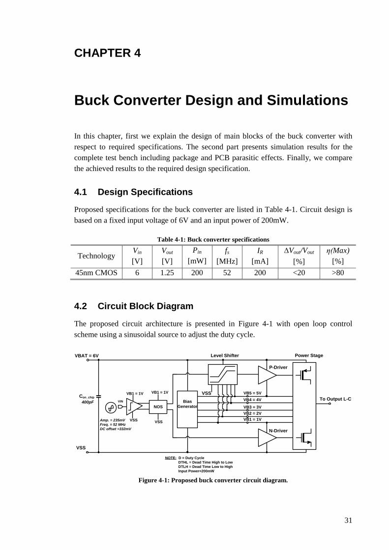
CHAPTER 4
Buck Converter Design and Simulations
In this chapter, first we explain the design of main blocks of the buck converter with
respect to required specifications. The second part presents simulation results for the
complete test bench including package and PCB parasitic effects. Finally, we compare
the achieved results to the required design specification.
4.1 Design Specifications
Proposed specifications for the buck converter are listed in Table 4-1. Circuit design is
based on a fixed input voltage of 6V and an input power of 200mW.
Table 4-1: Buck converter specifications
Technology Vin
[V]
Vout
[V]
Pin
[mW]
fs
[MHz]
IR
[mA]
∆Vout/Vout
[%]
η(Max)
[%]
45nm CMOS 6 1.25 200 52 200 <20 >80
4.2 Circuit Block Diagram
The proposed circuit architecture is presented in Figure 4-1 with open loop control
scheme using a sinusoidal source to adjust the duty cycle.
Figure 4-1: Proposed buck converter circuit diagram.
P-Driver
Level Shifter Power Stage
Amp. = 235mV
Freq. = 52 MHz
DC offset =332mV N-Driver
To Output L-C
VBAT = 6V
VB5 = 5V
VB1 = 1V
VB3 = 3V
VSS
VSSCon_chip
400pF
NOTE: D = Duty Cycle
DTHL = Dead Time High to Low
DTLH = Dead Time Low to High
Input Power=200mW
VB2 = 2V
VB4 = 4VBias
GeneratorNOS
VSS
VB1 = 1V VB1 = 1V
VIN
VSS
Page 38
32
Design procedure of each block and circuit operation is studied separately without con-
sidering the parasitic effects and then simulation results for the complete converter is
presented by including the parasitics.
4.3 Optimization of Power Stage
Design procedure of the power stage circuit is discussed in Section 3.1. This part inves-
tigates the optimization procedure to minimize total power loss and also modifications
that are required to achieve the reliable circuit operation. The main contributors to pow-
er loss are dynamic and static power loss mechanisms. Thus, to decrease total power
loss finding the optimum width of transistor is required. Power stage loss is simulated
for different transistor sizes and obtained result is shown in Figure 4-2. The NMOS
transistor width is selected as half of the PMOS transistor width because the electron
mobility of NMOS transistor is twice of the PMOS transistor and on-resistance depends
on the mobility according to equation (2.5).
Figure 4-2: Conversion efficiency for different PMOS transistor width values.
Applied method for transistor size selection does not ensure the minimum power loss by
itself because the other important factor is duty cycle that specifies the time duration
when transistor is on. Moreover switching loss is the other parameter that is different for
PMOS and NMOS transistors. Maximum power efficiency is achieved when transistor
widths are set to 11mm for PMOS and 5.5mm for the NMOS transistors.
4.4 Level Shifter
The other important block is the level shifter circuit that controls the power stage pull-
up and pull-down sequences by generating the driving signals for the outer stacked tran-
sistors. Since the required offset voltage is five times the nominal voltage (5V) accord-
ing to Figure 3-1, a high speed low to high voltage level shifter with efficient driving
84.8
85
85.2
85.4
85.6
85.8
86
86.2
86.4
86.6
6 8 10 12 14
Eff
icie
ncy(%
)
PMOS transistor Width (mm)
Page 39
33
capability is required; the circuit is designed based on three cascaded level shifters. First
and second stages are shifting the signal level by 2V and the third stage is used to shift
up the signal level by 1V with the circuit shown in Figure 4-3 (b). The proposed design
assures maximum supply voltage of 1V across each transistor terminals with respect to
45nm CMOS process requirements. Therefore, cascode configuration is proposed in the
level shifter circuit design.
Figure 4-3: (a) 2V level shifter circuit; (b) 1V conventional level shifter [15].
I. Design Procedure
Design procedure is only explained for the level shifter with an offset voltage of 2V as
shown in Figure 4-3 (a). The circuit consists of two ladder stages. Circuit design is
based on cascode structure to limit the voltage across transistors of the stage to a maxi-
mum voltage of 1V. Required gate bias voltages are shown in Figure 4-4 (a). Figure (b)
and (c) show the bias generation circuit for GP2 (2V/1V) and GN3 (1V/2V). Gate of
Mp4 is connected to output node with a voltage level of (3V/2V). Mp2 and Mn2 are
biased with fixed supply voltages.
Mn6
Mn7
Mp6
Mp7
Mpb2
Mnb2
Mn2
Mn3
Mp2
Mp3
Mpb1
Mnb1
1V
2V
1V
2V
1V
Cup
3V
Mp7 Mp4
Mn8
Mp5
Mn4
Mp1
Mn5 Mn1
Input
Output
3V
2V
GN7
GD2
GP6
P6S
P5S
P7S
N8S
N7S
N6S
P2S
P1S
P3S
N4S
N3S
N2S
GD1
GN5
GN6
GP2
Gn3
Mp4 Mp2
Mp3
Mn2
Mp1
Mn1
Cup
2V
V2 = 1V
V1 = 0V
V2 = 3V
V1 = 2V
Mn3
Mn4
2V
Output
V2 = 2V
V1 = 1V
InputV2 = 1V
V1 = 0V
1V 1V
1V
1V
I1
I2
I2
I1
(a) (b)
Page 40
34
Figure 4-4: (a) Level shifter switching operation; (b) bias for GN3 and (c) for GP2.
In low state when the output of level shifter is 2V, drain-source voltage across transistor
Mp2 is (1-Vth) because of diode connection of Mp1 and Mn4 that pulls-up the voltage
level of P1S in Figure 4-4 (a) to 2Vth. Same reason is applied for Mn3, voltage of N4S
is pull-down to 3V-2Vth then VDS for Mn3 is 1-Vth. For the case that diode connection
is not used in circuit, drain-source voltage for Mp2 and Mn3 will be raised to 1V+Vth
which is above 1V as maximum voltage for drain-source junction.
Coupling capacitor drives the inverter and speeds up the level shifter and therefore low-
er rise and fall times can be achieved which is required for high switching frequency
applications. An arbitrary capacitor value of 5pF is selected to achieve the voltage rising
( thV V ) that is required to drive the inverter circuit [15].
1
1par
DD
cup
VC
VC
(2.8)
parC is the parasitic capacitance at the gate node of Mp4. Both coupling and equivalent
parasitic capacitances are considered as series connections.
Transistor sizes of ladder circuit are selected small since there is no need to have small
on-resistance. Driving capability of the circuit depends on the requirements of the level
shifter for the rise and fall times. Inverter transistor size is selected with a bigger size to
fulfill the driving capability. Since a bigger size transistor adds more parasitic capaci-
tance at the gate node then there will be a need to increase the coupling capacitor value
Mn2
Mn3
Mp2
Mp3
1V
2V
Mp4
Mn4
Mp1
Mn1
Vth/3V-Vth
P2S:
P1S:
N3S:
N2S:
1V/2V
1V/0
2V/1V
3V/2V
3V
3V/2V
3V/2Vth
N4S:0/3V-2Vth
3V/1V+Vth
0/2V-Vth
0/1V-Vth
3V/1V+Vth
2V
Mnb1
GP2: 2V/1V
P2S:
1V
GN3:
N3S:
1V/2V
0/2V-VthMpb1
Output:
(a) (b) (c)
Page 41
35
according to equation (2.8). As a result there should be a compromise between inverter
transistor size and the coupling capacitor value.
Table 4-2: Transistor Sizes of level shifter circuit
Mn1,Mn3,Mn4
[um]
Mn2
[um]
Mp1,Mp3,Mp4
[um]
Mp3
[um]
Mnb1
[um]
Mpb1
[um]
10 60 20 80 10 20
II. Circuit Operation
In high state (3V) according to Figure 4-3 (a) for the input signal with 1V, output of
inverter (I1) is 0V. Coupling capacitor changes the second inverter (I2) input to 3 V .
The capacitor value is enough to satisfy thV V condition then the output of the sec-
ond inverter (I2) will be 3V. Mp7 will be switched off and P7S node that is connected to
Mp4 gate starts discharging, after it is discharged to 3V-Vth, Mp4 will be switched on.
P3S starts charging and when the node voltage is charged to 2V+Vth, Mp3 will be
switched on. Next P2S will start charging and then according to Figure 4-4 (c) Gp2 will
be charged to 2V.
For NMOS transistors Mn1 is switched off when output of I1 is 0V then N2S starts
charging until it reaches to 1-Vth. Then Mn2 will be switched off. N3S is charging to
2V-Vth and according to Figure 4-4 (b) GN3 will be charged to 2V. Mn4 is working in
triode region and after Mn3 is switched off N4S will be charged to 3-2Vth as shown in
Figure 4-4 (a).
For the output with low state (2V) circuit operates as follows. Circuit operation is start-
ed by transistor Mn1. first this transistor is switched on then N2S in Figure 4-4 (a) starts
discharging until Mn2 is switched on. Then N3S will be discharged, as illustrated in
Figure 4-4 (b) and GN3 will be discharged to 1V. Mn4 is biased in triode region with
VGS=Vth.
Regarding PMOS side operation, first coupling capacitor changes the inverter output to
3V then Mp7 will be switched off and P7S node that is connected to Mp4 gate starts
discharging, after it is discharged to 3V-Vth, Mp4 will be switched on. P3S starts charg-
ing and when the node voltage is charged to 2V+Vth, Mp3 will be switched on. Next
P2S will start charging and then according to Figure 4-4 (c) Gp2 will be charged to 2V.
III. Simulation Results
The level shifter circuit in Figure 4-3 (a) generates an output signal with a 2V offset and
following characteristics.
Page 42
36
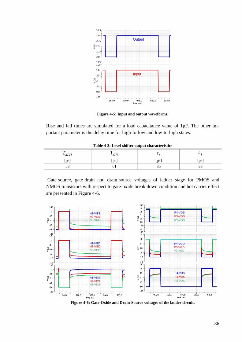
Figure 4-5: Input and output waveforms.
Rise and fall times are simulated for a load capacitance value of 1pF. The other im-
portant parameter is the delay time for high-to-low and low-to-high states.
Table 4-3: Level shifter output characteristics
dLHT
[ps]
dHLT
[ps]
r
[ps]
f
[ps]
53 61 35 33
Gate-source, gate-drain and drain-source voltages of ladder stage for PMOS and
NMOS transistors with respect to gate-oxide break down condition and hot carrier effect
are presented in Figure 4-6.
Figure 4-6: Gate-Oxide and Drain-Source voltages of the ladder circuit.
Output
Input
N2-VGD
N3-VGD
N1-VGD
N3-VDS
N1-VDS
N2-VDS
N1-VGS
N2-VGS N3-VGS
P3-VGD
P4-VGS
P2-VGD
P2-VDS
P4-VDS
P3-VDS
P3-VGS
P2-VGS
P4-VGD
Page 43
37
4.5 Global Bias Circuit
Global bias circuit provides the reference voltages that are used to generate the local
bias voltages for the gate of power stage. Two resistive ladder circuits in Figure 4-7 are
used. The first stage comprises of PMOS diode connected transistors and the second
stage includes NMOS diode connected transistors. These stages cannot sink or source
the current therefore another push-pull circuit at the output is used that mirrors the cur-
rent from ladder stages to the output.
Figure 4-7: Global bias circuit.
Transistors of the ladder circuit and push-pull circuit operate in the sub-threshold region
therefore bias current is limited to 24uA in ladder circuits. Charging and discharging of
the parasitic capacitance in output stage transistors consumes high currents. For this
reason on-chip decoupling capacitors are used to provide the current during switching
operation. As a result decoupling capacitors stabilize the generated output voltages by
keeping the transistors operation in the sub-threshold region.
VB4 = 4V
VB5 = 5V
VB2 = 2V
VB1 = 1V
VB3 = 3V
Mn1
Mp1
Mn2
Mp2
Mn3
Mp3
Mn4
Mp4
Mn5
Mp5
R1
Mnb1
R2
Mnb2
R3
Mnb3
R4
Mnb4
R5
Mnb5
R6
Mnb6
R7
Mpb2
R8
Mpb3
R9
Mpb4
R10
Mpb5
R11
Mpb6
R12
Mpb1
VBAT = 6V
VSS
C_onchip1
C_onchip2
C_onchip3
C_onchip4
C_onchip5
VSS
VSS
VSS
VSS
Page 44
38
Table 4-4: Component values for global bias circuit
Mnb1-Mnb6
[um]
Mpb1-Mpb6
[mm]
Mn1-Mn5
[mm]
Mp1-Mp5
[mm]
C1-C5
[pF]
R1-R12
[KΩ]
600 1.2 2 4 500 30
Simulation results:
Simulation results for the bias circuit are presented by using a test bench as shown in
Figure 4-8 to investigate the circuit performance under load condition.
Figure 4-8: Simulation test bench for studying the bias circuit performance.
Power stage contributes the main bias circuit current consumption and total power loss
of the converter. Moreover voltage instability during on/off states necessitates studying
the bias circuit operation by using the power stage as the load.
Figure 4-9: Output voltages of global bias circuit under load condition.
P-Driver
Level Shifter Power Stage
N-Driver
To Output L-C
VBAT = 6V
VB5 = 5V
VB1 = 1V
VB3 = 3V
VSS
VSS
VB2 = 2V
VB4 = 4VBias
GeneratorV2 = 1V
V1 = 0V
N-Drive
P-Drive
VDD
4.04V
4.03V
3.03V
3.02V
2.051V
2.053V
1.04V
1.01V
4VDD
3VDD
2VDD
5VDD
5.09V
5.03V
Page 45
39
Results show voltage instability in high and low states. In low state, gates of PMOS
transistors are discharged to off state voltage level as depicted in Figure 3-1 then high
current due to discharging of parasitic capacitance leads to a slight change in output
voltage level of the bias circuit.
4.6 Non-Overlapping Switching Circuit
Non-Overlapping switching circuit generates the required dead times for the power
stage circuit. Dead times are adjusted by the number of the inverters and generated de-
lay from inverter chain (I1-I10) and (I1-I14). Circuit operates in latch mode since the
next state of the circuit output depends on the previous states of Out1 and Out2.
Figure 4-10: Non-Overlapping Switching circuit.
The required number of inverters and dead time adjustment are achieved from the simu-
lation results for the test bench circuit shown in Figure 4-1.
Simulation results:
Acquired dead times for High-to-Low state is 159ps and 138ps for Low-to-High state.
Figure 4-11: Output waveforms of Non-Overlapping circuit
Out2_NOS
Out1_NOS
NOR Gate
NOR Gate
I1
V2 = 1V
V1 = 0V
I1 I10
1V
0V
1V
0V
1V
0V
I14
1V
0V
Input
Out1
Out2
Page 46
40
The reason for having different dead times is the induced delay by level shifter and
driver stages in signal propagation path. Achieved dead times for P-Drive and N-Drive
signals are proposed to be equal by investigating the simulation results and adjusting the
delay of inverter chain.
4.7 Schmitt Trigger
Open loop control scheme is based on using a simple Schmitt trigger circuit without
hysteresis characteristic to adjust the duty cycle of driving signals for the power stage as
illustrated in Figure 4-1. Input sinusoidal signal is applied at the input with an amplitude
of 235mV and an offset voltage of 324mV. Offset voltage should be selected below
threshold voltage to ensure the switching operation of the inverters including I1 and I2.
Amplitude and offset of the input signal specifies the duty cycle of the output signal. I3
and I4 are used for pulse shaping purpose.
Figure 4-12: Schmitt trigger circuit diagram.
Simulation results:
Input signal amplitude is increased from 400mV to 700mV and offset voltage has a con-
stant value of 200mV then the duty cycle of the output signal is changed from 34% to
28% according to Figure 4-13.
Figure 4-13: Schmitt trigger output waveform
M1
M2
0V
I1
1V
0V
I2
1V
1V
0V
Input Output
V2 = 1V
V1 = 0V0V
I3
1V
0V
I4
1V
Output
Input
Page 47
41
4.8 Filter Components
Filter components are selected with respect to buck converter specifications for output
voltage ripple, inductor current ripple and switching frequency. Therefore equations
(2.3) and (2.4) are used for the calculation of the filter components and obtained values
are L=100nH and C=100nH.
4.9 Parasitic Effects
Switching operation of the buck converter necessitates including the parasitic effects of
the measurement setup, IC package and non-idealities of the filter components in simu-
lation test bench. Switching noise is mainly due to parasitic inductive effects that gener-
ate the voltage ripple in signal propagation path. Buck converter test bench includes the
DC-DC converter blocks and parasitic components of the PCB and IC package. Package
parasitic, as depicted in Figure 4-14, consists of the lead frame and bonding wire ef-
fects. PCB parasitic originates from the trace and the component values in electrical
model depending on the trace width, length and switching frequency.
Figure 4-14: Electrical model of the PCB and package parasitic.
Electrical model of the package represents parasitic components of the WLB redistribu-
tion layer. In simulation test bench electrical model of the package represents the VCC-
Gnd for the VBAT and VSS pads and only lead frame and bonding wire model for Vx
signal as shown in Figure 4-14.
Rlead/2
Rlead/2
Rlead/2
Llead/2
Llead/2
Llead/2
Llead/2
Llead/2
Llead/2
Rlead/2
Rlead/2
Rlead/2
C12
C12
C
C
C13Lead1
Lead2
Lead3 C
LBond RBond
CBond
LBond RBond
CBond
LBond RBond
CBond
Bond1
Bond2
Bond3
LPCB RTrace
RTraceLPCB
RTraceLPCB
CPCBLPCB RTrace
LPCB RTrace
VDD
Gnd
Integ
rated
Circu
it
Rlead/2
Rlead/2
Llead/2
Llead/2 Llead/2
Rlead/2
Rlead/2C12
Llead/2
CBond
LBond RBond
LBond RBond
Package Lead
Frame Parascitics
Package Bonding
Wires Parascitics
Sig
na
ls
VC
C-G
nd
PCB Parasitics
Page 48
42
4.10 Simulation Test Bench
PCB layout design is based on minimum impact regarding parasitic effects that are gen-
erated by the traces. The effect of common ground on making the switching noise on
VSS pad will be demonstrated in simulation results.
Figure 4-15: Simulation Test Bench of the Buck converter.
DC
-DC
Co
nve
rte
r IC
VB
AT
RS
LS
Ba
tte
ry M
od
el
VD
D P
lan
e/T
race
L1
R1
R2
R4R3
L2
L3C
23
10
mW
10
mW
5mW
5mW
1n
H2
5n
H
18
0mW
10
0p
H
10
0p
H
R5
L4
L5C
45
20p
H
20
pH
R7
L6
L7C
67
5p
H
5p
H
50
mW
50
mW
5mW
5mW
10
0fF
40
0fF
2p
F
PC
B
Pa
ck
ag
e
VS
S
R6
R8
R9
L8
20
pH
50mW
C2
C3
C4
C1
R1
1L
9
10
0p
H5
mW
3mW
R1
0
10
mW
R0
Con_chip
IL
VB
AT
VX
L0
75W
@1
0M
Hz
Lo
ut
10
0n
H
Co
ut
VO
UT
Lf
RLoad
10
0n
F
75W
@1
0M
Hz
Page 49
43
Model of the battery is the static model of the lithium-ion type which includes only the
parasitic inductance and ESR and does not include state of charge. Decoupling capaci-
tors, and filter capacitor and inductor are used with real model in simulation test bench.
Table 4-5: Parasitic component of the PCB and package.
Value Purpose
R0 3mΩ Ground plane
R1, R2, R10 10mΩ Via+Trace Resistance
R3, R4, R11 5mΩ Trace Parasitics
L2, L3, L9 100pH Trace Parasitics
L1 1nH VDD Plane
C23 2pF PCB parasitic
R5, R6, R9 50mΩ Package parasitic
L4, L5, L8 20pH Package parasitic
R7, R8 5mΩ Package parasitic
L6, L7 5pH Package parasitic
Electrical model of the PCB and parasitic components values are obtained with the elec-
tromagnetic simulation of the PCB traces as the micro strip line. Different parasitic
components including the PCB trace parasitic, via, package parasitic and planes are
listed in Table 4-5.
Decoupling capacitors are used to decrease the switching noise of the supply voltage
line. C1 (4.7uF) is selected as the big capacitor that helps to improve the efficiency
since in high state, some part of the current is provided by discharging C1. This way the
current taken by the battery will be less in comparison to the case that we do not use the
capacitor and this can improve efficiency by decreasing the power consumption.
In order to reduce the switching noise effect, decoupling capacitors C1, C2 and C3 are
used with values listed in Table 4-6. Large capacitors have better performance with re-
spect to noise suppression however lower resonance frequency is the main limiting fac-
tor, thus small decoupling capacitors are connected in parallel to increase the total ad-
mittance.
Table 4-6: Discrete component values of the simulation test bench.
Value Manufacturer Part Number
L0 30Ω@100MHz MPZ1005S300CT000
C1 4.7 μF C1608X5R1A475M080AC
C2 100 nF C0603X5R1E104M030BB
C3 100 pF C0603X7R1E101K030BA
C4 2.2 nF C0603X7R1E222K030BA
Cout 100 nF C0510X6S0G104M030AC
Lout 100 nH MLZ1608DR10DT
Ls 25nH Battery model
Rs 180mΩ Battery model
RLoad 9.6Ω Ideal
Lf 30Ω@100MHz MPZ1005S300CT000
Page 50
44
Using the ferrite beads, L0 and Lf reduces the switching noise by suppressing the high
frequency noise components from the output and supply line of the PCB. Lout and Cout
are the filter parts that are selected according to buck converter specifications for the
inductor current ripple and output voltage ripple given in equations (2.3) and (2.4).
4.11 Simulation Results
This part is dedicated to simulation results that are achieved by including all buck con-
verter blocks, filter components, battery model, parasitic effects of the PCB and pack-
age. Simulation results are compared with the DC-DC converter specifications and fi-
nally required circuit modifications are proposed to achieve the target outputs.
4.11.1 Output Waveforms
Continuous conduction mode with an inductor current ripple of 200mA can be observed
from the converter output waveforms give in Figure 4-16. Circuit does not operate in
ZVS operation since inductor current direction is not changing during off state then Vx
node cannot be charged to battery voltage (6V) before switching to high state. ZVS op-
eration as explained in Section 3.2.5 provides smaller output voltage ripple because of
using smaller inductor with higher resonance frequency, however static power loss due
to high inductor current can decrease power efficiency.
Figure 4-16: Output waveforms of the buck converter.
Dead times are adjusted to avoid the body diode conduction but the values should be
selected large enough to increase the rise and fall times of Vx node to decrease the
switching noise at the output. Output voltage ripple and other issues are explained in the
next section.
-407mV
VX
IL
316mV
Vout
-350mV
28mA
197mV
201mA
Page 51
45
4.11.2 Switching Noise Effect
Including the parasitic effects in simulation test bench results in seeing the switching
noise effect at the output. Filter components have significant effect on switching noise.
Since an inductor with a low resonance frequency has a bigger parasitic capacitance
then charging and discharging of the parasitic capacitor during high-to-low and low-to-
high transition makes the switching current noise worse, as shown in Figure 4-16, and
this generates the voltage switching noise at the output. The other important noise con-
tributor is the PCB layout using the common ground scheme. High current flow from
output node to the ground through ground traces adds to the switching noise at the out-
put.
Figure 4-17: Switching noise effect on output signals.
Increasing the rise and fall times of Vx node decreases the switching noise of the induc-
tor current because parasitic capacitor of the inductor can be charged during the long
time duration. Noise ripple of the inductor current is shown in Figure 4-17. Increasing
VSS
Iin
Vout
IL
VX
VIN Chip
VIN Package
VBAT
67mA
45mV
36mV
319mV
252mV
342mV
283mV
316mV
197mV
256mA
29mA
294mV
240mV
-106mA
Page 52
46
the high-to-low and low-to-high dead times can increase the rise and fall times however
the possibility of body diode conduction will be increased if dead time is increased more
than a certain value, this also depends on the inductor value and current ripple. ZVS
operation improves circuit performance concerning output voltage switching noise as
illustrated in Section 3.2.5 because circuit design is based on smaller inductor value
with higher resonance frequency and higher dead time values.
Switching noise effect over the supply line of PCB can be seen in Figure 4-17 by start-
ing from the battery node and moving toward the input supply node of the chip for the
simulation test bench shown in Figure 4-15. Because of parasitic inductance of the PCB
traces, voltage ripple is increased towards the power supply.
Switching noise effect on global bias circuit is depicted in Figure 4-18 (a). Noise of the
input supply (VIN package) and VSS nodes generate the switching noise on global bias
circuit shown in Figure 4-17. Consequently driver signals are also affected from switch-
ing noise because of the noise effect on bias signals. Switching noise effect on gate bias-
ing of the power stage should be studied carefully since noise ripple can increase the
gate-oxide voltage to more than the maximum allowed voltage of 1.1V.
(a) (b)
Figure 4-18: Switching noise effect on bias voltages (a) and driving signal (b).
Increase of gate-source voltage in low-to-high transition points is due to the longer dead
time and inductor current direction that decreases the source voltages below the on-state
voltage. Since circuit does not operate in ZVS operation then inductor current cannot
charge source nodes.
According to switching sequence of NMOS transistors, N1 will be switched earlier
therefore voltage drop is more significant for N2S. As depicted in Figure 4-19 (a) VGS
is increased to 1.3V. Selecting a smaller inductor value and changing the inductor cur-
rent direction helps to charge the source nodes which can mitigate the voltage rise
5VDD
4VDD
3VDD
2VDD
VDD
P-Drive
Package
N-Drive
Page 53
47
condition during low-to-high dead time; however small inductor current increases the
inductor current ripple to more than 200mA which is not complied with buck converter
specifications.
(a) (b)
Figure 4-19: VGS and VDS for NMOS power stage transistors.
(a) (b)
Figure 4-20: VGS and VDS for PMOS power stage transistors.
Voltage rise of VDS for N6 is because of the smaller charge of N6S. GNP in off state is
5V then source will charge up to 5V-Vth, as a result P6S according to Figure 3-1 is ap-
proximately 6V then VDS will increase to 1V+Vth. Same operation for three cascode
stage is illustrated in Section 2.4.3, equation (2.7).
N1-VGS
N2-VGS
N3-VGS
N4-VGS
N5-VGS
N6-VGS
N1-VDS
N2-VDS
N3-VDS
N4-VDS
N5-VDS
N6-VDS
1.43V
1.31V
1.24V
1.16V
1.25V
1.21V
1.11V
1.26V
P1-VGS
P2-VGS
P3-VGS
P4-VGS
P5-VGS
P6-VGS
P1-VDS
P2-VDS
P3-VDS
P4-VDS
P5-VDS
P6-VDS
1.25V
1.71V
1.63V
1.42V
1.83V
1.31V
1.25V
Page 54
48
Switching noise effect for PMOS transistors as shown in Figure 4-20 is considerable in
comparison to NMOS transistors because noise effect on input supply node of package
(VBAT) is higher than VSS. The noise effect is decreasing towards upper stacked tran-
sistors due to bias circuit topology. Moreover PMOS transistor size is larger than
NMOS and the parasitic capacitance of the source node will be larger in comparison to
NMOS transistors. Large transistor size increases the switching delay of PMOS stacked
transistors that leads to voltage overshoot because source nodes cannot be charged at the
same rate.
4.11.3 Power Conversion Efficiency
Efficiency of the complete test bench is obtained by calculating the power loss for all
parts of the simulation test bench. Thus efficiency of the converter is defined as the ratio
of the output power that can be delivered to load and input power which is supplied
from the battery node.
Input power is adjusted to 207mW using the output load of RL=9.6 Ω and duty cycle of
21% according to buck converter specifications then achieved power efficiency is
79.2%.
Table 4-7: Power efficiency results of the buck converter
Efficiency
[%]
Input Power
[mW]
Output Power
[mW]
Vout
[V]
Vinput
[V]
fs
[MHz]
DTHL
[ps]
DTLH
[ps]
79.2 207 164 1.25 6 52 190 189
Power stage has the major contribution in total power loss with a value of 27mW as
depicted in Figure 4-21. Optimization of the power stage has considerable effect on ef-
ficiency improvement by selecting the appropriate transistors sizes. The other important
source of power loss is the output inductor with a power loss of 7mW due to high ESR
and low quality factor.
Bias circuit power loss is the other main source of loss with a value of 2.1mW that is
generated by the resistive ladder circuit shown in Figure 4-7. Transistors of the ladder
circuit and output push pull stage should operate in sub threshold region with low qui-
escent current. High output current is required to charge and discharge the gate capaci-
tance of the power stage transistor. However, decoupling capacitors used in circuit can
provide the current during transition between states. Charging and discharging of the
decoupling capacitors during high and low states causes the power loss.
Package lead resistance also contributes with a high power loss which is 2.46mW. Pow-
er loss distribution is only presented for the non-ZVS operation for a required inductor
current ripple of (200mA). Results for ZVS operation in 3.2.5 show better performance
Page 55
49
regarding switching noise effect. However, high inductor current ripple can increase the
static power loss. Therefore, there should be a compromise between efficiency and
switching noise ripple.
Figure 4-21: Power loss contributions.
0
5
10
15
20
25
30
35
40
[mW
]
NMOS (Power Stage) PMOS (Power Stage)
Inductor Global Bias
N-Drive P-Drive
Level Shifter PCB
Package NOS
Ferrite Beads Capacitor
Schmitt triger
Page 56
50
CHAPTER 5
Buck Converter with Variable Battery
Supply
In this chapter, a buck-type DC-DC converter is presented that is capable of operation
under variable input battery voltage from 3.5V to 6V. The proposed converter is based
on a new design technique using an adaptive biasing circuit and cascode power stage
implemented in 45-nm CMOS technology. Dynamic biasing is used to generate the gate
biasing voltages of the transistors according to the variations in the battery voltage level.
The converter achieves a maximum power conversion efficiency of 81% for an output
voltage of 1.25V and an output power of 200mW.
5.1 Proposed Circuit
The proposed buck converter as shown in Figure 5-1 consists of a power stage circuit
with four cascode transistors, an adaptive gate biasing circuit, two inverter chains as
gate drivers and external filter components. Nominal breakdown voltage of gate-source
and gate-drain junctions for the used CMOS technology is 1.8V. This requires using
four cascode transistors for a reliable circuit operation with a maximum battery voltage
of 6V. The adaptive gate biasing circuit presented in this paper is designed to configure
itself according to the supply battery voltage and generate fixed 1.5V gate-source and
gate-drain voltages for cascode transistors in the power stage in on and off states, re-
spectively. SW and CP signals are the outputs of the switch controller and comparator
circuits shown in Figure 5-2. The input to the comparator is a function of the battery
voltage through the resistive voltage divider and the reference input to the comparators
is 1.5V. For VBAT above 4.5V the output of the comparator is CP=1.5V and when VBAT
is below 4.5V, CP=3V. The comparator circuit has an adjustable hysteresis characteris-
tic that is used to eliminate voltage variations due to switching noise [17]. Hysteresis
value is considered to be 36mV as depicted in Figure 5-3(a). Therefore, comparator
output switches when VBAT=4.5V±18mV.
Circuit diagram of the switch controller used to generate SW signal according to the
battery voltage level is shown in Figure 5-2.The comparator output signal CP is used as
an input to the switch controller circuit. The switch controller circuit consists of three
cascode transistors in the output stage for a safe operation under a maximum voltage of
VBAT-1V= 5V. Two cascode stages with differential switch operation mode provide the
gate bias for cross coupled pairs (P5, P8). For 4.5V±18mV<VBAT<6V, CP=1.5V and
Page 57
51
transistors P8, P9 and P10 are switched on and SW=VBAT-1V. When
3.5V<VBAT<4.5V±18mV, CP=3V and transistors N8, N9 and N10 are switched on and
SW=1.5V. Outputs of the comparator and switch controller circuits are presented in
Figure 5-3(b).
Figure 5-1: Buck converter with cascode power stage.
The gate biasing circuit in Figure 5-1 is designed to operate in different modes based on
battery voltage values as shown in Table 5-1. When 4.5V<VBAT, SW and CP signals
create open states (Ns and Ps are off). In this case, when the output voltage VX=VBAT,
transistors Nb1, Nb2 and Nb3 are on and Pb1, Pb2 and Pb3 are off. Common node
(GN4/GP4) and GP3 are biased with VBAT-1.5V and GN3 is biased with 3V. When
VX=0V, transistors Pb1, Pb2 and Pb3 are on while Nb1, Nb2 and Nb3 are off. (GN4/GP4)
and GN3 are biased with 1.5V and GP3 is biased with VBAT-3V. This ensures that for
this range of battery voltage, the gate-source and gate-drain voltages of all transistors
stay within 1.5V less than the breakdown voltage.
N4
N3
N2
N1
P1
P2
P3
P4
Nb2
Nb1C1
C2NsCP
VBAT -3V
VBAT -1.5V
3V
Ps C3
C4
Pb2
Pb1
Nb3
SW
1.5V
VBAT
VX
Cf
Lf
RL
VOUT
200µm
0.15µm
18pF
9pF
5pF
10pF
100nH
100nF 7.8Ω
SP2
SP3
SP4
SN4
SN3
SN2
Pb3
6mm0.15µm
12mm0.15µm
ND
1.5V
PD
VBAT
VBAT -1.5V
GP2
GP3
GP4
GN4
GN3
GN2
0.15µm
400µm
Gate Bias Circuit
Page 58
52
Figure 5-2: Comparator and Switch controller circuits.
Figure 5-3: (a) Hysteresis curve for comparator circuit and (b) comparator and switch controller
circuit outputs.
Table 5-1: Different modes of gate bias circuit
VBAT VX CP SW Ps Ns
4.5V<VBAT<6V 0 1.5V VBAT-1V Open Open
4.5V<VBAT<6V VBAT 1.5V VBAT-1V Open Open
3.5V<VBAT<4.5V 0 3V 1.5V Open Short
3.5V<VBAT<4.5V VBAT 3V 1.5V Short Short*
*Ns is open for 4.5-Vth< VBAT <4.5V
CP
3V
1.5V
1.5V
VBAT
Rk2
Rk1
1.5V
3V
VBAT -1V
VBAT-2.5V
SW
N8
N10
N9
P8
P9
P10
Nb4Nb5
Pb4Pb5
100µm
0.15µm
50µm
0.15µmN5
N7
N6
P5
P6
P7
SN6
SN7
GP7
GN7
SP7
SP6
SP9
SP10
SN10
SN9
320nm
0.15µm
320nm
0.15µmGP10
GN10
(a) (b)
VBAT (V)
CP
(V
)
36mV
4.518V4.482V
VBAT-1VVBAT-1V
VBAT =3.5V
3V
1.5V
1.5V
6V 6V
VB
AT (
V)
CP
(V
)S
W (
V)
Page 59
53
For VBAT<4.5V and when VX=0V, Pb1 and Pb2 are switched on, CP=3V and creates a
short state while SW=1.5V creates an open state (Ps is off and Ns is on). Therefore GP3,
GN3 and GN4/GP4 are all biased with 1.5V. For VBAT<4.5V and when VX=VBAT, Nb1
and Nb2 are switched on, SW= 1.5V creates a short state (Ps is on). Therefore GP3,
GN3 and GN4/GP4 are all biased with VBAT-1.5V.
Figure 5-4 shows simulated gate bias voltages for gate nodes GN3, GP3 and
GN4/GP4. As shown in Figure 5-4(a), for VX=VBAT, when VBAT>4.5V, GN3 is biased
at a fixed voltage of 3V. The slight variation from 3V is due to the fact that transistor
Nb3 in Figure 5-1, is operating in the sub-threshold region. However, the other two
nodes, GP3 and GN4/GP4 have a bias voltage equal to VBAT-1.5V over the entire range
of 3.5V<VBAT<6V. Figure 5-4 (b) shows gate bias voltages when VX is at low state. In
this case, all the nodes are biased at 1.5V except GP3. For 4.5V<VBAT, GP3 is connect-
ed to VBAT-3V source. The slight variation from VBAT-3V is due to the fact that Pb3 is
operating in the sub-threshold region. Using the proposed gate bias circuit, for the entire
battery voltage range of 3.5V<VBAT<6V, the gate-source voltage of power transistors in
the on state is equal to 1.5V which is required to achieve minimum on resistance and
subsequently minimum conduction loss while maintaining enough safety margin from
the breakdown voltage.
Figure 5-4: Gate bias voltages. (a) VX at High State and (b) VX at Low State
Switching operation of the power train transistors in Figure 5-1 is controlled by driv-
er pulse signals PD and ND with rise and fall times of 100ps and frequency of 50MHz.
Gate driver circuits consisting of inverters are used to bias P1 and N1 transistors. Gate
node voltages are synchronized with these driver signals. Decoupling capacitors C1 to
C4 are also used to suppress voltage overshoot in gate nodes caused by coupling effect
of large parasitic capacitors. Capacitance values are selected to provide the same RC
delay time and therefore same discharge rate at the gate nodes of all transistors in the
power stage.
0
0.5
1
1.5
2
2.5
3
3.5
4
4.5
5
3.5 4 4.5 5 5.5 6
GP3
GN4/GP4
GN3
VBAT (V)
0
0.5
1
1.5
2
2.5
3
3.5
3.5 4 4.5 5 5.5 6
GP3
GN4/GP4
GN3
VBAT (V)
Vo
lta
ge
(V
)
VBAT -3V
Pb3 in sub-threshold
VBAT -1.5V
VBAT -1.5VNb3 in sub-threshold
(a) (b)
Vo
lta
ge
(V
)
Page 60
54
5.2 Simulation Results
The proposed DC-DC buck converter is simulated for different supply battery voltage
values in Cadence using 45nm Generic PDK. Figure 5-5 shows simulated transient node
voltages for each transistor within the power stage for VBAT=6V. In low-to-high transi-
tion of the output voltage VX, power stage switching operation starts with P1 when PD
is VBAT-Vth. Gate nodes of PMOS transistors (GP) are sequentially charged to 4.5V and
source nodes (SP) are charged to approximately 6V, with small voltage drop because of
on-resistance as shown in Figure 5-5(a). Gate and source voltage of NMOS transistors
are also plotted in Figure 5-5. Dead times for both low-to-high and high-to-low transi-
tions are 116ps to prevent short circuit conduction in the power stage. Therefore, during
the 116ps dead time, both P1 and N1 transistors are off.
Figure 5-5: Transient node voltages for VBAT=6V. (a) low-to-high and (b) high-to-low tran-
sitions.
Switching operation for high-to-low transition of the power stage output VX, as
shown in Figure 5-5(b), starts with N1 when ND is higher than threshold voltage. The
gate and source voltages of NMOS transistors are sequentially discharged to 1.5V and
0V, respectively. The steady state value of gate voltages of both NMOS and PMOS
transistors are according to the values shown in Figure 5-4 for VBAT=6V.
GN
(V
)V
X (
V)
SN
(V
)N
D (
V)
PD
(V
)G
P (
V)
SP
(V
)
SP2SP3SP4
5.98V
4.5V
3V
1.5V
4.5V
6V
4.5V
1.5V
0V
GP2GP3GP4
VX
4.5V
3V
1.5V
4.11V2.66V1.22V
5.95V
GN2GN3GN4
SN2SN3SN4
6V-Vth
Vth
116ps
4.75V
3.27V1.78V
6V-Vth
116ps
Vth
-35mV
(b)(a)
Page 61
55
Figure 5-6 shows the simulated output waveforms for the designed buck converter.
The output voltage for the power stage VX, inductor current IL and the output voltage of
the converter Vout are plotted for three different values of VBAT=3.5V, 4.8V and 6V. The
buck convertor operates in continuous conduction mode with a maximum inductor cur-
rent ripple of 200mA for VBAT=6V. Vout is maintained at a constant voltage value of
1.25V with a maximum switching noise of 350mV. The switching noise in IL and Vout
can be improved by using a high-Q inductor with lower parasitic capacitance and higher
resonance frequency in the output filter. For the discrete inductor Lf=100nH we have
used spice model of a TDK SMD inductor in our simulation [18]. The simulated power
conversion efficiency for the designed buck convertor is shown in Figure 5-7. A peak
power conversion efficiency of 81.3% is achieved for VBAT at 3.9V and it stays above
72% for the entire range of the battery voltage from 3.5V to 6V.
Figure 5-6: Buck Converter Output Waveforms.
Figure 5-7: Simulated Power Conversion Efficiency.
VBAT=6VVBAT=4.8V
VBAT=3.5V
Vo
ut (
V)
I L (m
A)
VX (
V)
70
72
74
76
78
80
82
84
3.5 4 4.5 5 5.5 6
Eff
icie
ncy(%
)
VBAT (V)
Page 62
56
CHAPTER 6
Conclusions
The main objective of this thesis is to design an integrated buck converter for an input
voltage value of 6V based on 45nm advanced CMOS technology. Cascode structure is
proposed in the design of the power stage circuit to avoid reliability issues regarding
gate-oxide breakdown and hot carrier effects.
In order to assure the voltage limit of 1V across transistor terminals, gate nodes should
be biased dynamically according to on/off states. The bias circuit that is an important
part of the design, generates the gate voltages for each one of the transistors with respect
to its operating state.
The other important part of the work is the level shifter circuit that controls the power
stage pull-up and pull-down sequences by generating the required driving signal for the
outer stacked transistor. Since the required offset voltage is five times the nominal volt-
age (5V), a high speed low to high voltage level shifter with efficient driving capability
is required; the circuit is designed based on three cascaded level shifters.
In order to achieve higher efficiency off-chip components are used in filter part. The
main drawback using discrete components is the low resonance frequency. As a result,
charge and discharging of the parasitic capacitance will considerably increase the induc-
tor current ripple and voltage ripple at the output. In addition, parasitic inductance of
PCB traces has significant effect on switching noise therefore proper layout is the other
important part of the design.
The circuit architectures are evaluated using generic 45nm CMOS technology to im-
plement the DC-DC Converter with a switching frequency of 52MHz. Proposed buck
converter provides an output voltage of 1.25V with an efficiency of 79.2% for an input
power of 207mW. Complete models of the package and PCB by considering the parasit-
ic effects have been carefully taken into account in simulations.
A converter is proposed that can operate under variable supply battery voltage from
3.5V to 6V. The dynamic operation is achieved by using a novel biasing circuit that
operates in different modes. The biasing circuit ensures a reliable operation of all the
transistors with respect to a maximum breakdown voltage of 1.8V in 45nm CMOS. The
output voltage of the converter is constant at 1.25V and the power conversion efficiency
is better than 72% for the entire range of VBAT=3.5V to 6V. The output power of the
Page 63
57
convertor is 200mW for an output load of RL=7.8 Ohm and the power density defined
as power per inductor area is 195mW/mm3 for a 100nH TDK SMD inductor.
Page 64
58
REFERENCES
[1] US383759 Lithium Polymer battery datasheet available at:
http:// www.sony.com.cn/products/ed/battery/download.pdf , Date: 10.10.2014.
[2] Hazucha, P.; Sung Tae Moon; Schrom, G.; Paillet, F.; Gardner, D.; Rajapandian, S.; Karnik, T.,
"High Voltage Tolerant Linear Regulator With Fast Digital Control for Biasing of Integrated
DC-DC Converters," Solid-State Circuits, IEEE Journal of , vol.42, no.1, pp.66,73, Jan. 2007.
[3] Chang-Joon Park; Onabajo, M.; Silva-Martinez, J., "External Capacitor-Less Low Drop-Out
Regulator With 25 dB Superior Power Supply Rejection in the 0.4–4 MHz Range," Solid-State
Circuits, IEEE Journal of , vol.49, no.2, pp.486,501, Feb. 2014.
[4] Wens, Mike, Steyaert, Michiel,” Design and Implementation of Fully-Integrated Inductive DC-
DC Converters in Standard CMOS”, Springer 2011, Chapter 2, Page 36.
[5] Villar-Pique, G.; Bergveld, H.J.; Alarcon, E., "Survey and Benchmark of Fully Integrated
Switching Power Converters: Switched-Capacitor Versus Inductive Approach," Power Electron-
ics, IEEE Transactions on , vol.28, no.9, pp.4156,4167, Sept. 2013.
[6] E. S-Sinencio, A. Andreou, “Low-Voltage / Low-Power Integrated Circuits and Systems”,
Chapter 12, Wiley-IEEE Press, 1998.
[7] A. J. Stratakos, “High-efficiency, low-voltage dc–dc conversion for portable applica-
tions", Ph.D. dissertation, Dept. Electr. Eng., Comput. Sci., Univ. California, Berkeley, 1998.
[8] Serneels, Bert, Steyaert, Michiel,” Design of High Voltage xDSL Line Drivers in Standard
CMOS”, Springer 2008.
[9] Varghese, D.; Mathur, G.; Reddy, V.; Heater, J.; Krishnan, S., "Simulation and modeling of hot
carrier degradation of cascoded NMOS transistors for power management applications," Relia-
bility Physics Symposium (IRPS), 2012 IEEE International , vol., no., pp.3B.3.1,3B.3.4, 15-19
April 2012.
[10] Bandyopadhyay, S.; Ramadass, Y.K.; Chandrakasan, A.P., "20 μA to 100 mA DC–DC Con-
verter With 2.8-4.2 V Battery Supply for Portable Applications in 45 nm CMOS," Solid-State
Circuits, IEEE Journal of , vol.46, no.12, pp.2807,2820, Dec. 2011.
[11] Xiao, J.; Peterchev, A.V.; Zhang, Jianhui; Sanders, S.R., "A 4-μa quiescent-current dual-mode
digitally controlled buck converter IC for cellular phone applications," Solid-State Circuits,
IEEE Journal of , vol.39, no.12, pp.2342,2348, Dec. 2004.
[12] Hyunseok Nam; Youngkook Ahn; Jeongjin Roh, "5-V Buck Converter Using 3.3-V Standard
CMOS Process With Adaptive Power Transistor Driver Increasing Efficiency and Maximum
Load Capacity," Power Electronics, IEEE Transactions on , vol.27, no.1, pp.463,471, Jan. 2012.
[13] Kuttner, F.; Habibovic, H.; Hartig, T.; Fulde, M.; Babin, G.; Santner, A.; Bogner, P.; Kropf, C.;
Riesslegger, H.; Hodel, U., "A digitally controlled DC-DC converter for SoC in 28nm CMOS,"
Solid-State Circuits Conference Digest of Technical Papers (ISSCC), 2011 IEEE International ,
vol., no., pp.384,385, 20-24 Feb. 2011.
[14] Serneels B., M.Steyaert, W.Dehaene, “A 237mW aDSL2+ CO Line Driver in Standard 1.2V
0.13μm CMOS”, IEEE-ISSCC, San Francisco 2007, pp.524-525,619.
Page 65
59
[15] Serneels, B.; Steyaert, M.; Dehaene, W., "A High speed, Low Voltage to High Voltage Level
Shifter in Standard 1.2V 0.13μm CMOS," Electronics, Circuits and Systems, 2006. ICECS '06.
13th IEEE International Conference on , vol., no., pp.668,671, 10-13 Dec. 2006.
[16] J. Stratakos, “High-efficiency, low-voltage dc–dc conversion for portable applications", Ph.D.
dissertation, Dept. Electr. Eng., Comput. Sci., Univ. California, Berkeley, 1998.
[17] P.Amiri, A.Nabavi and S.Y. Mortazavi,”Low distortion CMOS class-D amplifier with dou-
ble-band hysteresis”, IEICE Electronics. Express, Vol. 7, No. 4, P 273-280, 2010.
[18] TDK: MLZ1608DR10DT SPICE Netlist (2015) http://product.tdk.com
Page 66
60
APPENDIX-1: A manuscript as the outcome of thesis work is submitted to IEICE Electronics Express
Title: A High Efficiency DC-DC Buck Converter with Variable Battery Supply in
45nm-CMOS Technology
Authors: Arash Fouladi, Jani Jarvenhaara, Nikolay. T. Tchamov
Submission Date: 16.0.9.2015
Abstract: In this paper, a buck-type DC-DC converter is presented that is capable
of operation under variable input battery voltage from 3.5V to 6V. The proposed
converter is based on a new design technique using an adaptive biasing circuit and
cascode power stage implemented in 45-nm CMOS technology. Dynamic biasing is
used to generate the gate biasing voltages of the transistors according to the varia-
tions in the battery voltage level. The converter achieves a maximum power conver-
sion efficiency of 81% for an output voltage of 1.25V and an output power of
200mW.