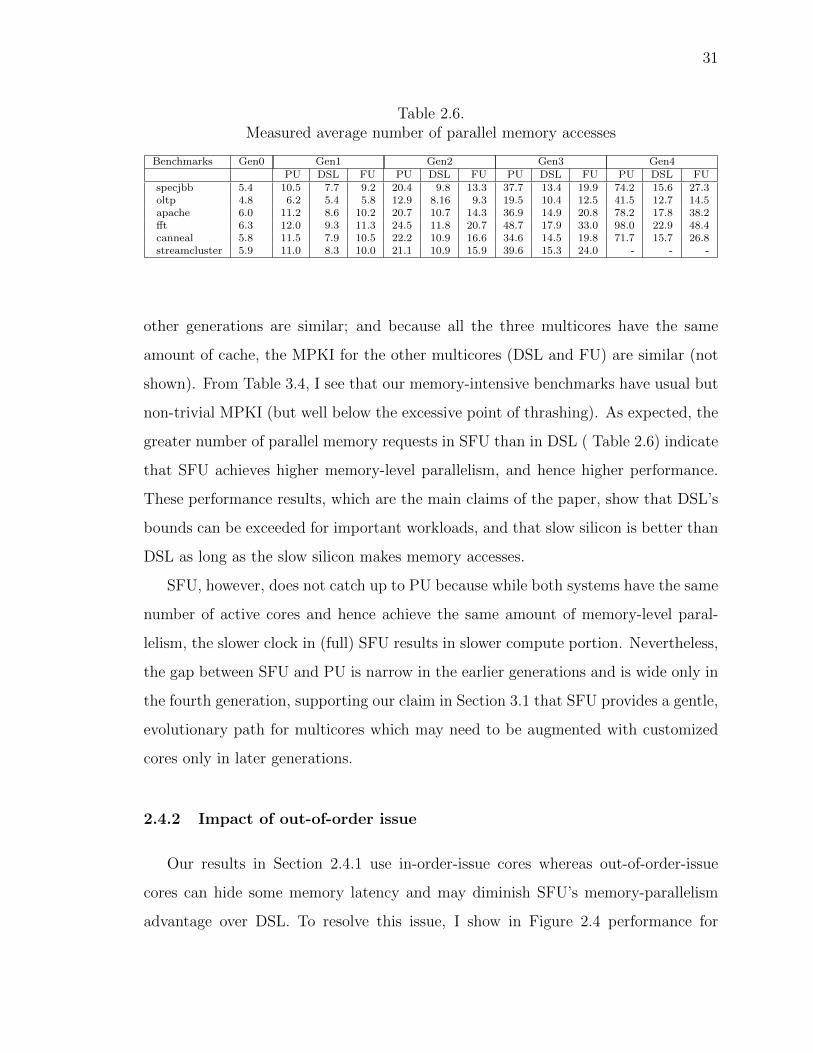
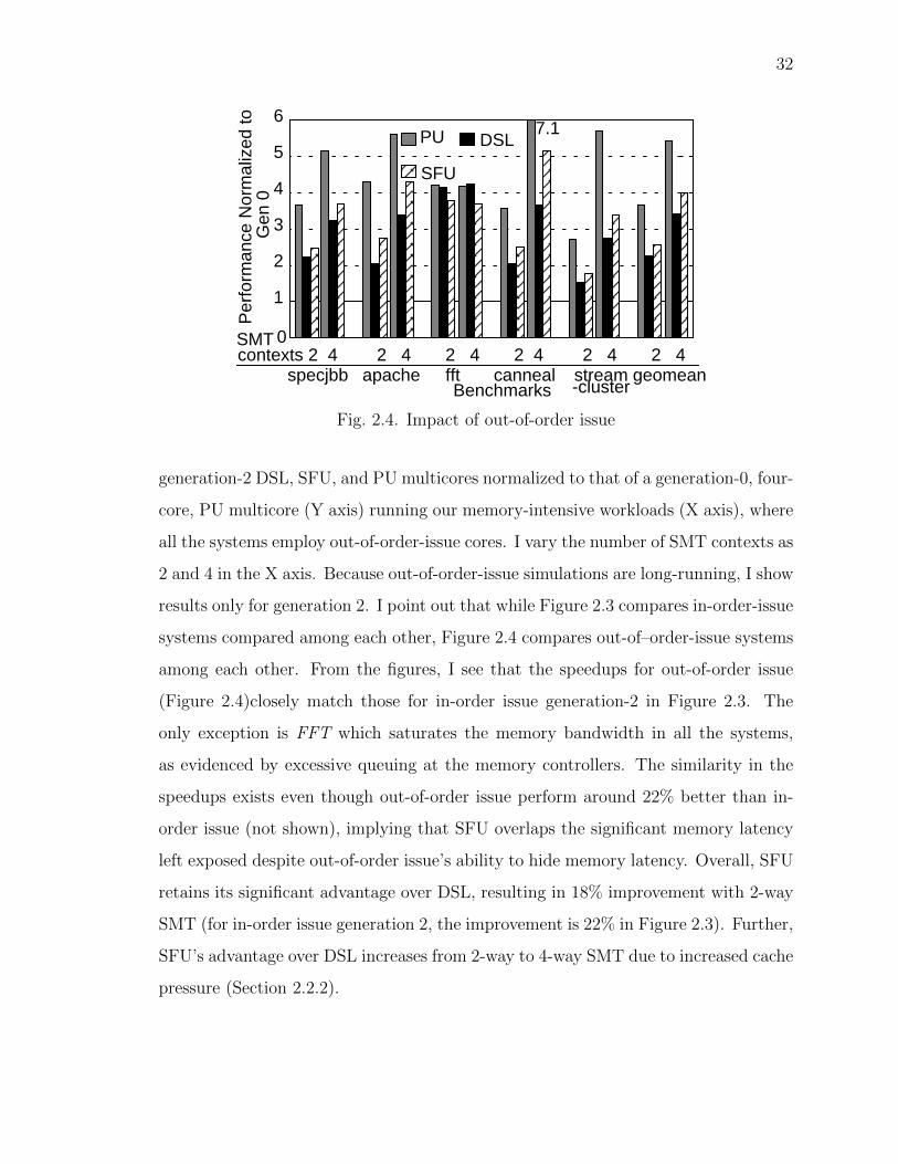
Purdue University Purdue e-Pubs Open Access Dissertations eses and Dissertations Spring 2015 Architectural techniques to extend multi-core performance scaling Hamza Bin Sohail Purdue University Follow this and additional works at: hps://docs.lib.purdue.edu/open_access_dissertations Part of the Computer Engineering Commons , and the Computer Sciences Commons is document has been made available through Purdue e-Pubs, a service of the Purdue University Libraries. Please contact [email protected] for additional information. Recommended Citation Sohail, Hamza Bin, "Architectural techniques to extend multi-core performance scaling" (2015). Open Access Dissertations. 559. hps://docs.lib.purdue.edu/open_access_dissertations/559
Transcript
Purdue UniversityPurdue e-Pubs
Open Access Dissertations Theses and Dissertations
Spring 2015
Architectural techniques to extend multi-coreperformance scalingHamza Bin SohailPurdue University
Follow this and additional works at: https://docs.lib.purdue.edu/open_access_dissertations
Part of the Computer Engineering Commons, and the Computer Sciences Commons
This document has been made available through Purdue e-Pubs, a service of the Purdue University Libraries. Please contact [email protected] foradditional information.
Recommended CitationSohail, Hamza Bin, "Architectural techniques to extend multi-core performance scaling" (2015). Open Access Dissertations. 559.https://docs.lib.purdue.edu/open_access_dissertations/559
To the best of my knowledge and as understood by the student in the Thesis/Dissertation Agreement, Publication Delay, and Certification/Disclaimer (Graduate School Form 32), this thesis/dissertation adheres to the provisions of Purdue University’s “Policy on Integrity in Research” and the use of copyrighted material.
Hamza Bin Sohail
Architectural Techniques to Extend Multi-core Performance Scaling
2.1 Speedups across generations of PU, DSL, and SFU multicores over a four-core multicore (generation 0) for the following workloads: (a) mostly se-rial and memory-unintensive, (b) mostly serial, and memory-intensive,(c) mostly parallel and memory-unintensive, and (d) mostly parallel andmemory-intensive . . . . . . . . . . . . . . . . . . . . . . . . . . . . . . 22
2.2 Sensitivity to model parameters (speedup relative to generation 0, 4-coreconfiguration) for the different values of m and s: (a) Variable memoryintensity with s = 0.01, (b) Variable parallelism with m = 0.8 . . . . . 23
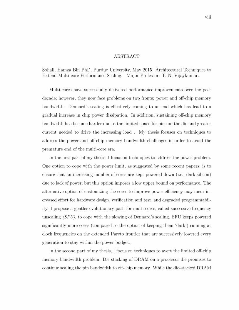
Sohail, Hamza Bin PhD, Purdue University, May 2015. Architectural Techniques toExtend Multi-core Performance Scaling. Major Professor: T. N. Vijaykumar.
Multi-cores have successfully delivered performance improvements over the past
decade; however, they now face problems on two fronts: power and off-chip memory
bandwidth. Dennard’s scaling is effectively coming to an end which has lead to a
gradual increase in chip power dissipation. In addition, sustaining off-chip memory
bandwidth has become harder due to the limited space for pins on the die and greater
current needed to drive the increasing load . My thesis focuses on techniques to
address the power and off-chip memory bandwidth challenges in order to avoid the
premature end of the multi-core era.
In the first part of my thesis, I focus on techniques to address the power problem.
One option to cope with the power limit, as suggested by some recent papers, is to
ensure that an increasing number of cores are kept powered down (i.e., dark silicon)
due to lack of power; but this option imposes a low upper bound on performance. The
alternative option of customizing the cores to improve power efficiency may incur in-
creased effort for hardware design, verification and test, and degraded programmabil-
ity. I propose a gentler evolutionary path for multi-cores, called successive frequency
unscaling (SFU), to cope with the slowing of Dennard’s scaling. SFU keeps powered
significantly more cores (compared to the option of keeping them ‘dark’) running at
clock frequencies on the extended Pareto frontier that are successively lowered every
generation to stay within the power budget.
In the second part of my thesis, I focus on techniques to avert the limited off-chip
memory bandwidth problem. Die-stacking of DRAM on a processor die promises to
continue scaling the pin bandwidth to off-chip memory. While the die-stacked DRAM
ix
is expected to be used as a cache, storing any part of the tag in the DRAM itself erodes
the bandwidth advantage of die-stacking. As such, the on-die space overhead of the
large DRAM cache’s tag is a concern. A well-known compromise is to employ a small
on-die tag cache (T$) for the tag metadata while the full tag stays in the DRAM.
However, tag caching fundamentally requires exploiting page-level metadata locality
to ensure efficient use of the 3-D DRAM bandwidth. Plain sub-blocking exploits this
locality but incurs holes in the cache (i.e., diminished DRAM cache capacity), whereas
decoupled organizations avoid holes but destroy this locality. I propose Bandwidth-
Efficient Tag Access (BETA) DRAM cache (β$) which avoids holes while exploiting
the locality through various metadata organizational techniques. Using simulations,
I conclusively show that the primary concern in DRAM caches is bandwidth and not
latency, and that due to β$’s tag bandwidth efficiency, β$ with a T$ performs 15%
better than the best previous scheme with a similarly-sized T$.
1
1. INTRODUCTION
For the past several decades, Moore’s law has been the driving force behind the
computing industry. The doubling of transistors every 2 years and increasing tran-
sistor speed at the same dollar cost delivered exponential performance improvement.
In 1974, Robert Dennard presented the scaling theory for CMOS which postulated
that transistors can be shrinked, and key figures of merit such as operating speed,
layout density and energy efficiency can be improved as long as voltages, geometric
dimensions and doping concentrations are consistently scaled to maintain constant
electric field [1]. Dennard’s scaling has been the major enabling factor in delivering
the promise of Moore’s law. During the earlier process generations, constant voltage
scaling was employed but with almost a linear increase in power consumption, the
industry switched to constant electric field scaling.
However, the slowing of Dennard’s scaling during the last decade due to higher
static power at lower threshold voltages forced the industry to move to multi-cores.
Multi-cores were inevitable since uniprocessor performance improvements were only
sustainable if Dennard scaling had continued. Multi-cores ushered the era in which
higher performance necessitated greater parallelism in applications. Going parallel to
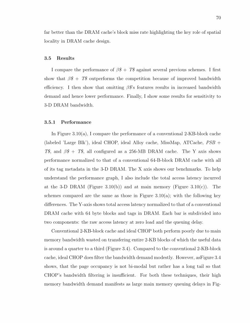
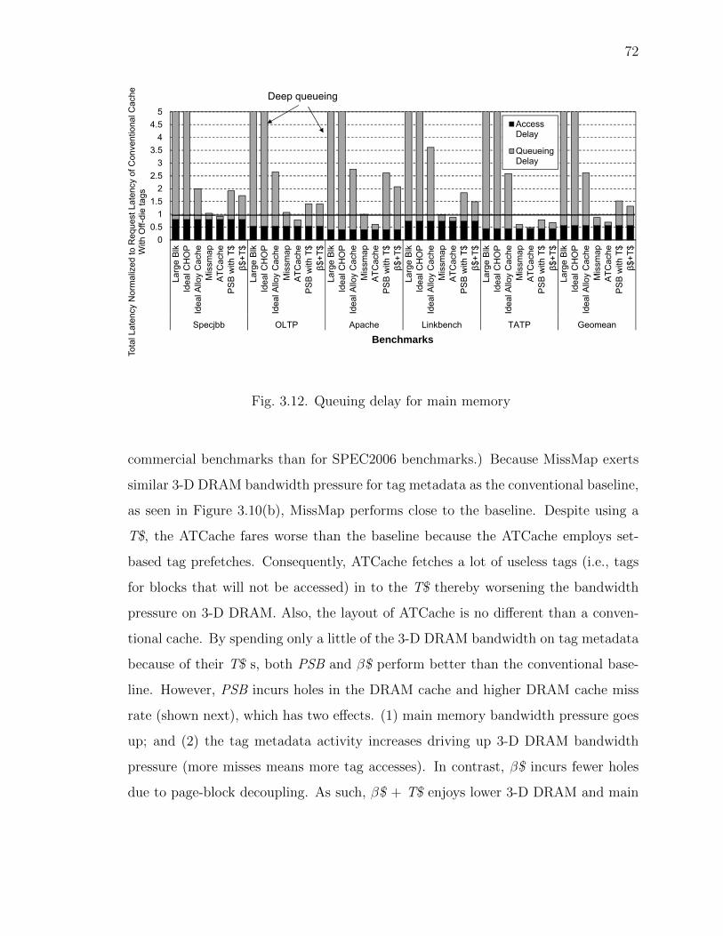
sustain Moore’s law was a major change in the landscape of computing. Multi-core
performance came through exploitation of thread-level parallelism and small improve-
ments in clock frequency. While multi-cores have successfully delivered performance
improvements over the past decade, they now face problems on two fronts: power and
off-chip memory bandwidth. Figure 1.1 shows chip power consumption over the years
and extrapolates the effects of Dennard’s scaling coming to an end. Purportedly, the
imminent end of Dennard scaling will result in multi-cores hitting a utilization wall –
a direct implication of the power wall. With supply voltage no longer scaling, many
architects feel a significant number of transistors simply cannot be activated because
2
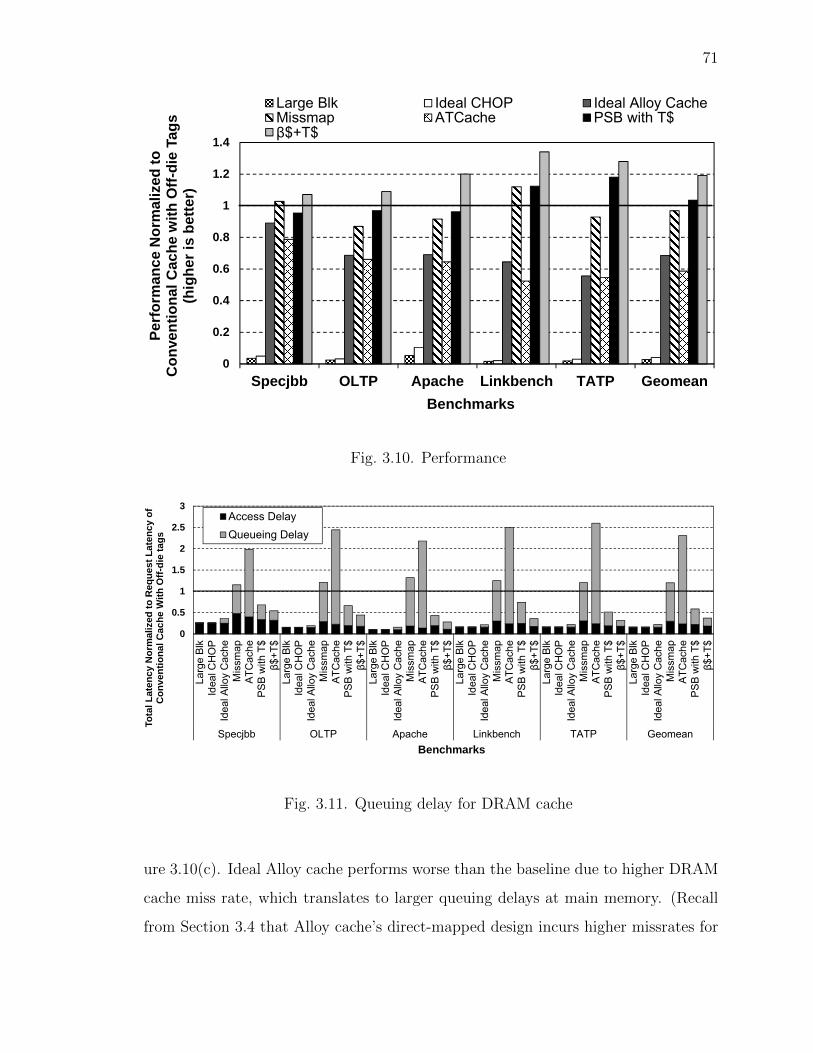
TDP of power-unconstrained system
End ofDennard’s scaling
Projection
Desired TDP
2015 2020 2025 2030
400300200100
TDP (W)
Fig. 1.1. Power projections (The trends have been extrapolated fromthe power trends figure courtesy of Kunle Olukotun and Lance Ham-mond)
of stringent power constraints.
In Chapter 2, I present an alternate evolutionary path for multi-core scaling in
the absence of Dennard’s scaling that can alleviate the power problem and extend the
life-span of the multi-core era. I argue that architects, so far, have ignored the fact
that memory plays a central role in today’s applications; from databases to webservers
and beyond, memory plays a crucial role in limiting the achievable performance. Be-
cause the power limits are harsh for memory-unintensive application behavior, the
memory-intensive nature of a vast number of today’s applications can act as a boon
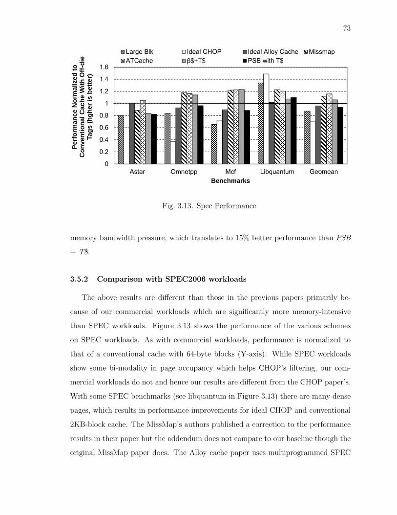
rather than a bane for multi-cores.
3
I/O Pads
1x Transistors 2x Transistors 4x Transistors
Die
Fig. 1.2. Pin count increase with double the cores
In addition to the power conundrum, today’s multi-cores have an increasing de-
mand of memory bandwidth. Doubling the cores, even with double the cache capacity,
increases the memory bandwidth demand by a factor of 2 which necessitates increas-
ing the off-chip memory bandwidth. However, increasing off-chip memory bandwidth
requires increase in pin count as well as device bandwidth. While heavy banking of
DRAM will increase the device bandwidth, bus bandwidth requires an increase in pin
count of the processor chip. Since die sizes do not change, it has become increasingly
difficult to add more pins to increase bus bandwidth due to the limited space for pins
on the die and greater current needed to drive the increasing load. 3-D Die-stacking
aims to alleviate the pin-bandwidth problem. 3-D Die-stacked DRAM is stacked on
top of the chip while Through-Silicon-Vias (TSVs) act as the interface between the
chip and DRAM. Because the vias are on the surface of the chip and not the edges,
it allows for more and wider buses. Even if DRAM is not stacked on top of the pro-
cessor die, it can still offer high bandwidth by being off-die but in the same package
(e.g., Intel’s Haswell GT3e integrates a 128 MB DRAM in the same package). 3-D
Die-stacking is meant to reduce the off-chip traffic which reduces the off-chip memory
bandwidth demand. Consequently, the need to increase pin count can be avoided.
However, the effectiveness of 3-D Die-stacking depends on how well its main feature
(i.e., bandwidth) is used. As conventional wisdom suggests, researchers have proposed
4
designing 3-D Die-stacked caches that reduce the off-chip memory traffic. The pri-
mary reason for this choice is that the capacity of 3-D Die-stacked DRAM is still far
less than what off-chip DDR3/DDR4 modules have to offer; it adds negligible capac-
ity to the physical address space if it were to be added as on-package physical memory.
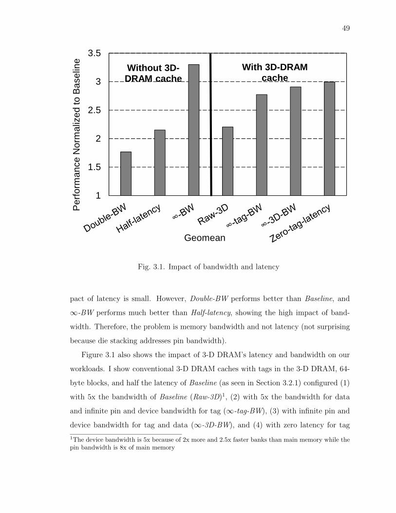
In Chapter 3, I explore the design challenges associated with 3-D Die-stacked
caches. The main advantage of 3-D Die-stacked caches is its high bandwidth. While
it may provide some latency benefits (the smaller size of arrays and shorter delays on
TSVs may reduce access delay), it is really the bandwidth of 3-D-Die stacked DRAM
which enables it to serve the memory demands of multi-cores. First, I conclusively
show how bandwidth (and not latency) is the real feature of 3-D Die stacked caches,
contrary to some recent papers which tend to argue otherwise. Second, I show the
importance of metadata organization in 3-D Die-stacked DRAM in order to preserve
the bandwidth advantages that 3-D Die-stacking has to offer. Chapter 3 shows that
plain-subblocking, a cache design technique invented back in the 1960s, tends to
exploit spatial locality in a way that helps in cutting down the bandwidth demand
due to metadata accesses. However, plain sub-blocking exploits this locality but
incurs holes in the cache (i.e., diminished DRAM cache capacity), whereas decoupled
organizations avoid holes but destroy this locality. To satisfy these seemingly opposing
contraints, Chapter 3 will describe Bandwidth-Efficient Tag Access (BETA) DRAM
cache (β$), a cache design which avoids holes while exploiting the locality through
various metadata organizational techniques with the aim to preserve the bandwidth
advantage provided by 3-D Die-stacked DRAM.
Chapter 4 wraps up the thesis with conclusions drawn from the earlier chapters,
and ends with greater optimism for the future of multi-cores.
5
2. COPING WITH THE SLOWING OF DENNARD’S
SCALING
2.1 Introduction
Historically, CMOS scaling has reduced transistor area and per-transistor dynamic
power by about half and has improved switching speed by about 40% from one tech-
nology generation to the next. Specifically, Dennard’s scaling of the supply voltage
has allowed doubling the number of transistors without significantly worsening the
dynamic power [1]. Recently, however, on one hand, Dennard’s scaling has slowed
down significantly due to its undesirable side-effects of higher leakage, narrower noise
margins, and worse reliability (e.g., supply voltage reduces only by 2% now). On
the other hand, transistor count, and hence the number of cores in a multicore, con-
tinue to double. Consequently, there is an exponential divergence between the core
count and the per-core power. Unfortunately, the total chip power budget cannot
be increased due to limits on cooling and power delivery (i.e., the total chip power
will remain constant). These trends imply an increasing power shortage in future
generations.
The imminence of dark silicon – silicon that must be kept deactivated because of
power shortage – has been presaged1 for some time now [2]. A recent paper [3] ana-
lyzes these trends and asserts that an increasing number of cores must be deactivated
in future generations and that future multicore performance is fundamentally limited
by dark silicon. I refer to the previously shown, dark-silicon induced multicore perfor-
mance limit in [3] as (DSL). Alternatively, to alleviate the resulting performance loss,
other papers [4–6] have suggested customizing the cores for specific functionalities to
improve power efficiency and activate more cores with the same power budget. Unfor-
1ARM CTO Mike Muller appears to have coined the term “dark silicon”. [2]
6
tunately, the customization option puts multicores on a potentially arduous path of (i)
requiring customization to provide exponential improvements of power efficiency (i.e.,
every generation better than the previous), (ii) incurring increased effort for hardware
design, verification, and test, and (iii) potentially degraded programmability.
In this paper, I show that DSL performance bounds can be exceeded for memory-
intensive applications, and that a gentler, evolutionary path exists where customiza-
tion may be optional but not essential. Previous dark silicon papers [3, 5] examine
design points along the power-performance Pareto frontier covering a large space of
large and small core designs and voltage-frequency-scaled operating points. The pa-
pers assert that the DSL configurations, in which a subset of the cores run at the
Pareto-optimal clock speed while the rest are deactivated, achieves the best possible
performance for a given technology generation and power budget. I emphasize that
DSL deactivates cores and thereby bounds the peak power to be within the budget.
I make three key observations: First, because voltage-scaling has slowed down
considerably, the Pareto frontier extends to a new region derived by frequency scaling
alone. Second, because memory lags far behind processor clocks in speed, perfor-
mance of most realistic workloads for future multicores will be dominated by memory
latency and not processor clock speed (most future multicores with 16 or more cores
are destined for servers with memory-intensive workloads). Finally, because cores
wait for memory in such workloads and thereby dissipate far less power than the
peak, DSL’s average power is well below the budget. Our key result combines the
first two observations to show that lower frequencies on the new extended Pareto fron-
tier enable powering of more or, in many cases, all cores of a multicore which achieve
more memory-latency overlap and better performance than DSL limits. I show that
our results hold despite techniques for reducing, hiding, or tolerating memory latency
via 3-D stacked memory, out-of-order issue, and simultaneous multithreading, respec-
tively. While the DSL configuration bounds its peak power by deactivating cores (i.e.,
in space), I do so by lowering the clock frequencies (i.e., in time). However, our mul-
ticores’ better performance does imply higher average power than DSL’s well-below-
7
the-budget average. Nevertheless, as I show later in Section 2.2.2, our multicores’
average power is guaranteed to be within the budget.
I arrive at our key result by exploiting two known non-linear effects, the first
of which is captured by a simple analytical model for multicore performance. Our
model shows that in the degenerate case of absence of memory latency, more cores
running at slower clocks perform similarly to fewer running at faster clocks under the
same power budget as long as the workloads are sufficiently parallel (a condition also
necessary for multicores in general). In the presence of memory latency, however,
more cores running at slower clocks perform better than fewer cores running at faster
clocks. This reversal occurs because of the non-linear impact of clock speed on per-
formance in the presence of memory latency where more active cores achieve more
overlap of memory latency so that the dominant memory component of execution
time reduces far more than the slight increase in the smaller non-memory component
due to the slower clock. While our extra cores do incur more leakage than the DSL
cores (cache capacity, and therefore cache leakage, is the same in both cases), SFU’s
advantage over DSL remains for memory-intensive workloads even after accounting
for this extra leakage in all but extreme cases (e.g., 90% of the chip power is in
leakage). However, because adjusting for the extra-leakage does modestly degrade
memory-unintensive workloads, I propose to revert to the DSL configuration for such
workloads. Thus, our key insight is that, for a broad range of memory-intensive com-
mercial and scientific workloads, slow silicon is better than DSL’s dark silicon as long
as the slow silicon makes memory accesses. While voltage scaling has historically
exploited the non-linear (cubic) relationship between power and voltage, I propose
that clock-performance non-linearity be exploited in the post-Dennard era. Due to
this fundamental non-linearity, DSL’s performance limit can be exceeded for many
realistic and important multicore workloads.
Based on our model’s predictions, I propose a gentler, evolutionary path for multi-
cores than customization, called successive frequency unscaling (SFU). In SFU, more
cores than DSL (and in many cases, all cores) are kept activated and run at succes-
8
sively slower clocks every generation to bridge the exponential divergence between the
core count and per-core power in the post-Dennard era. While the linear relationship
between power and frequency is well known, this paper is the first to propose suc-
cessively slower clocks; dynamic voltage and frequency scaling (DVFS) dynamically
changes the clock speed up or down for good power-performance within a technology
generation but does not employ successively slower clocks from one generation to the
next.
I employ SFU in two contexts with different performance metrics. In the first
context of workloads where job execution time is the only metric (e.g., scientific
applications), I employ full SFU wherein I unscale frequency to power all the cores.
Surprisingly, despite considerably slower clocks in later generations (e.g., sub-GHz)
full SFU exceeds the DSL performance limit. Not surprisingly, however, SFU does
not completely close the gap between a DSL configuration and a power-unconstrained
system due to the slower clock. In the other context of enterprise workloads (e.g., on-
line transaction processing) where both throughput and response latency matter, the
slower clock of full SFU would degrade single-thread performance, and hence response
latency. Accordingly, I employ controlled successive frequency unscaling (C-SFU)
which moderately slows down the clock and powers many, if not all, cores to achieve
better throughput than DSL. C-SFU avoids degrading response latency despite the
clock slowdown by exploiting the second non-linearity that the higher throughput of
C-SFU non-linearly reduces the queuing component of response latency and thereby
compensates for the slower clock. Finally, SFU’s simplicity implies better performance
at virtually no design effort or complexity, enabling a viable evolutionary path for
multicores.
The key contributions of this paper are:
• I propose the unusual idea of successively slower cores to stay within the power
budget in the post-Dennard era.
9
• I show that, for memory-intensive applications (which includes important com-
mercial benchmarks) our approach can exceed the DSL’s performance limits.
The key results of this paper are:
• for memory-intensive workloads, SFU performs 46% better than DSL’s limits at
the 11 nm technology node whereas for memory-unintensive, workloads I revert
to the DSL configuration; and
• for response-time-sensitive enterprise workloads, C-SFU achieves 21% better
throughput than DSL at the 11 nm technology node while maintaining the
total response latency including queuing delays to be within +/- 10%.
• while out-of-order cores partially reduce opportunity for SFU by reducing the
exposed memory latency, there remains ample opportunity for SFU to improve
performance compared to DSL (e.g., SFU with out-of-order cores achieves 18%
better performance then DSL with out-of-order cores at the 22nm technology
node).
The rest of the paper is organized as follows. Section 2.2 discusses our intuition and
qualitative arguments behind SFU, and then presents a simple power-performance
model for multicores to provide quantitative corroboration of our intuition. Sec-
tions 2.3 and 3.5 validate our model using simulations of commercial and scientific
workloads. Finally,
2.2 Multicore power and performance
I start with the intuition behind SFU followed by an analytical model.
2.2.1 Intuition
The two key claims by Esmailzadeh et al. [3] are that (1) the limit on perfor-
mance achievable in practical multicore systems of future technology generations is
10
significantly lower than the performance of a power-unconstrained multicore system
in the equvalent technology generation, and (2) dark-silicon is inevitable for opti-
mal performance. Esmailzadeh et al.do not examine frequency scaling alone because,
where both voltage and frequency scaling are possible, scaling frequency alone is
not Pareto-optimal. However, in regions where further voltage scaling is infeasible,
frequency-scaling alone can be used to extend the power-performance Pareto fron-
tier. Even in this extended Pareto frontier, frequency scaling alone cannot improve
upon DSL for memory-unintensive applications (i.e., applications with little exposed
memory latency) because both techniques offer the same linear improvement (degra-
dation) in performance for linear increase (reduction) in power. However, I observe
that when I include the effect of exposed memory latency, the power-performance
tradeoff due to frequency unscaling becomes sub-linear because the exposed memory
latency does not scale. Such sublinearity is advantageous because a large reduction in
frequency (which reduces power linearly) results in less-than-proportional reduction
in performance. This difference in the impact of frequency scaling on dynamic power
(linear) and performance (sub-linear) is central to enabling our design to achieve
higher performance than the DSL limits would imply.
Recent work [7] reveals that near-threshold operation is performance-per-watt
optimal for perfectly parallelizable programs. Given that the dark-silicon problem
is to maximize performance under a fixed power-budget, one may think that such
performance-per-watt optimality is ideal. However, near-threshold-computing’s en-
ergy optimality results in very slow speed (e.g., 3-MHz Intel Claremont). As such,
even though individual cores may be performance-per-watt optimal, the system as a
whole will run into other bottlenecks (e.g., area, application scalability) which can
prevent the utilization of the full power budget and hence degrade performance. Fur-
ther, the paper does not consider memory effects which is the main focus of our
work.
11
Next, to support the above qualitative reasoning, I develop a simple analytical
model of the combined impact of SFU’s frequency unscaling and memory latency
effects on overall multicore power-performance.
2.2.2 Model
Our model is derived from Amdahls’ Law [8] and more recent revisits of Amdahl’s
Law in the context of multicores [3,9]. However, recall from Section 3.1 that the key
reason for our better performance is more cores achieving higher overlap of mem-
ory latency. Accordingly, our model specifically includes memory latency effects in
addition to the usual serialization effects.
I first describe our model for a multicore that is not constrained by power. Then,
I modify this model to include power constraints either via the DSL configuration or
successive frequency unscaling (SFU). Let
• s be the serial portion of sequential execution time (i.e., 1 − s is the parallelportion);
• c be the factor by which the clock frequency improves every technology gener-ation (e.g., if the clock speed improves by 20% then c = 1.2); and
• m be the fraction of sequential execution time due to memory latency (i.e.,1−m is the non-memory, compute fraction).
I derive m as follows: Assuming the number of off-chip misses per kilo instructions
(MKPI) is r, the per-access average exposed main memory latency is memlat in
processor cycles, and the processor cycles per instruction (CPI) with 0% off-chip miss
rate is instrlat then
m = r ×memlat/(1000× instrlat + r ×memlat).
For example, assuming an off-chip miss rate of 2% which usually corresponds to r
of 5, memlat of 400, and instrlat of 0.5 gives m = 0.80. I note that memlat denotes
exposed memory latency, and hence covers both in-order- and out-of-order-issue cores
though the latter’s memlat and m values would be smaller than the former’s.
To simplify the model, I assume that
12
• both the parallel and serial portions of the application incur the same fractionm of execution time due to memory latency;
• employing more parallel cores does not change the fraction m of execution timedue to memory (our experimental evaluation avoids these two assumptions byusing real workloads);
• the factor c is constant across generations while in reality clock speed improve-ments may reduce in later generations resulting in an overall average of c (ourexperimental evaluation uses actual, non-constant factors);
• the cores do not employ simultaneous multithreading (SMT) (I include SMTlater); and
• memory bandwidth scales with the number of cores (I revisit this assumptionin our results).
Defining the execution time on the generation-0 system as 1 (i.e., our normaliza-
tion base), the breakdown of the total execution time may be expressed as:
s× ((1−m) +m) + (1− s)× ((1−m) +m)
Over n technology generations, the non-memory, compute fraction 1 − m scales
as (1 − m)/cn due to clock speed improvements while the memory fraction m re-
mains unchanged. This scaling occurs for both the serial and parallel portions so
that the serial portion scales as s × (1−mcn
+ m) and the parallel portion scales as
(1 − s) × (1−mcn
+ m). In addition, the parallel portion gets further sped up by a
factor of 2 every generation due to the doubling of the core count so that the parallel
portion scales overall as
(1− s)× (1−mcn
+m)
2n.
Thus, after n generations since the last uniprocessor, a power-unconstrained (PU)
multicore achieves a net speedup of
1
s× (1−mcn
+m) +(1− s)× (
1−mcn
+m)
2n
(2.1)
I note that while the 1 −m compute terms in both the serial and parallel portions
diminish exponentially over generations due to faster clocks, the m memory term
13
in the parallel portion diminishes exponentially due to more cores’ higher memory-
level parallelism. For memory-intensive workloads, m is generally greater than 1−m
making the number of cores more important than the clock speed for performance
(from the above example, m is 0.80). As I will see shortly, this difference is the key
contrast between DSL and SFU where the former keeps only a subset of the available
cores powered whereas the latter keeps all the cores powered albeit at a slower clock.
For the DSL multicore which is constrained by power, let p be the factor by which
the per-core dynamic power scales every technology generation due to a combination
of feature size scaling, slow scaling of voltage, and transistor engineering (e.g., if power
reduces by 20% then p = 0.8). To simplify the model, I assume that
• the dynamic power of the on-chip (non-L1) caches and network for a core’saccesses are included in the core’s dynamic power (an accounting simplificationthat does not affect the model’s predictions);
• leakage is zero (I add in leakage in the next section); and
• p, like c, is constant across generations while in reality dynamic power improve-ments may reduce in later generations resulting in an overall average of p.
To stay within the constant power budget across generations, DSL bounds its peak
power by limiting the number of cores after n generations to (2 × 0.5/p)n = 1/pn
(i.e., bound in space). DSL differs from PU only in the number of active cores
—- 1/pn versus 2n; DSL enjoys identical clock speed and last-level, shared cache
size improvements, and incur similar memory latency effects. Therefore, the DSL
multicore’s net speedup after n generations is
1
s× (1−mcn
+m) +(1− s)× (
1−mcn
+m)
1/pn
(2.2)
I see that DSL exploits significantly less memory-level parallelism than PU due to
fewer active cores. This limitation considerably degrades performance for realistic
multicore workloads which are memory-intensive.
14
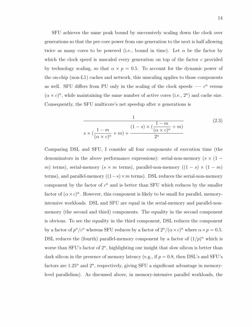
SFU achieves the same peak bound by successively scaling down the clock over
generations so that the per-core power from one generation to the next is half allowing
twice as many cores to be powered (i.e., bound in time). Let α be the factor by
which the clock speed is unscaled every generation on top of the factor c provided
by technology scaling, so that α × p = 0.5. To account for the dynamic power of
the on-chip (non-L1) caches and network, this unscaling applies to those components
as well. SFU differs from PU only in the scaling of the clock speeds —– cn versus
(α× c)n, while maintaining the same number of active cores (i.e., 2n) and cache size.
Consequently, the SFU multicore’s net speedup after n generations is
1
s× (1−m
(α× c)n+m) +
(1− s)× (1−m
(α× c)n+m)
2n
(2.3)
Comparing DSL and SFU, I consider all four components of execution time (the
denominators in the above performance expressions): serial-non-memory (s × (1 −
m) terms), serial-memory (s × m terms), parallel-non-memory ((1 − s) × (1 − m)
terms), and parallel-memory ((1−s)×m terms). DSL reduces the serial-non-memory
component by the factor of cn and is better than SFU which reduces by the smaller
factor of (α×c)n. However, this component is likely to be small for parallel, memory-
intensive workloads. DSL and SFU are equal in the serial-memory and parallel-non-
memory (the second and third) components. The equality in the second component
is obvious. To see the equality in the third component, DSL reduces the component
by a factor of pn/cn whereas SFU reduces by a factor of 2n/(α×c)n where α×p = 0.5.
DSL reduces the (fourth) parallel-memory component by a factor of (1/p)n which is
worse than SFU’s factor of 2n, highlighting our insight that slow silicon is better than
dark silicon in the presence of memory latency (e.g., if p = 0.8, then DSL’s and SFU’s
factors are 1.25n and 2n, respectively, giving SFU a significant advantage in memory-
level parallelism). As discussed above, in memory-intensive parallel workloads, the
15
parallel-memory component is likely to dominate the other components, magnifying
SFU’s advantage. Therefore, DSL’s limit can be exceeded.
Impact of leakage:
The above analysis ignores leakage power, which generally increases with lower
supply voltage and higher transistor count. In the post-Dennard generations, how-
ever, leakage as a fraction of the total power budget will either remain a constant
(e.g., 25-30%) or increase only slowly (e.g., under 5% per generation) due to two rea-
sons: (1) voltage scaling has slowed down considerably and (2) the rate of growth of
transistor speed over generations is reduced to compensate for the doubling of tran-
sistor count every generation (e.g., by fine-tuning the transistor threshold voltage).
Recent commercial microprocessors follow this methodology to keep leakage under
check [10]. Note, I assume SFU and DSL use the same fast, leaky transistors (i.e.,
per-transistor leakage is the same for SFU and DSL). This assumption enables us to
operate a subset of processors with the same maximum frequency as DSL which is
important to allow for memory-unintensive workloads.
Let l be the leakage budget as a fraction of the total power budget in the last
uniprocessor generation and λ be the rate at which the total chip leakage budget
increases every generation. Then, the chip leakage budget scales as λn × l after n
generations (to be meaningful, λn × l < 1 for any n), whereas the chip dynamic
power budget scales as (1 − λn × l). To make room for leakage, this new dynamic
power budget is lower than our previously-assumed full budget. Let fl be the core
leakage as the fraction of the total chip leakage, the remainder of which is the cache
leakage. This scaling implies that (1) the core counts and clock frequencies for DSL
and SFU, respectively, should be adjusted for this new dynamic power budget at every
generation; and (2) DSL’s fewer cores incur less leakage than the allotted budget (and
also less than SFU), allowing more cores to be added (the DSL paper does not discuss
such compensation).
16
Because the new, lower dynamic power budget is the same for DSL and SFU, both
designs are affected similarly. Both DSL’s core count for generation n, given by 1/pn,
and SFU’s clock frequency, given by (α × c)n in Equations 2.2 and 2.3, respectively,
reduce by the factor (1−λn × l). Therefore, SFU maintains its advantage in memory-
level parallelism, and hence performance, over DSL.
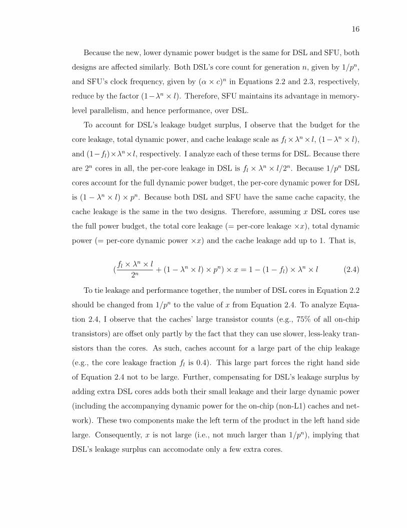
To account for DSL’s leakage budget surplus, I observe that the budget for the
core leakage, total dynamic power, and cache leakage scale as fl×λn× l, (1−λn × l),
and (1−fl)×λn×l, respectively. I analyze each of these terms for DSL. Because there
are 2n cores in all, the per-core leakage in DSL is fl × λn × l/2n. Because 1/pn DSL
cores account for the full dynamic power budget, the per-core dynamic power for DSL
is (1 − λn × l) × pn. Because both DSL and SFU have the same cache capacity, the
cache leakage is the same in the two designs. Therefore, assuming x DSL cores use
the full power budget, the total core leakage (= per-core leakage ×x), total dynamic
power (= per-core dynamic power ×x) and the cache leakage add up to 1. That is,
(fl × λn × l
2n+ (1− λn × l)× pn)× x = 1− (1− fl)× λn × l (2.4)
To tie leakage and performance together, the number of DSL cores in Equation 2.2
should be changed from 1/pn to the value of x from Equation 2.4. To analyze Equa-
tion 2.4, I observe that the caches’ large transistor counts (e.g., 75% of all on-chip
transistors) are offset only partly by the fact that they can use slower, less-leaky tran-
sistors than the cores. As such, caches account for a large part of the chip leakage
(e.g., the core leakage fraction fl is 0.4). This large part forces the right hand side
of Equation 2.4 not to be large. Further, compensating for DSL’s leakage surplus by
adding extra DSL cores adds both their small leakage and their large dynamic power
(including the accompanying dynamic power for the on-chip (non-L1) caches and net-
work). These two components make the left term of the product in the left hand side
large. Consequently, x is not large (i.e., not much larger than 1/pn), implying that
DSL’s leakage surplus can accomodate only a few extra cores.
17
I illustrate this point with some realistic examples based on known scaling trends [4].
Assume a constant 30-70 split of the total budget for leakage and dynamic power (i.e.,
l = 0.3 and λ = 1) and a 40-60 split of the leakage budget for the cores and caches
(i.e., fl = 0.4). Assume generation 6 with 64 cores (i.e., n = 6) and DSL’s p = 0.646
(i.e., p6 = 0.073). While SFU runs all the 64 cores at a slower clock, DSL runs 1/p6
= 13.7 cores at the full clock speed. SFU splits a total budget of 100 as 12, 70, and
18 for the core leakage, dynamic power, and cache leakage, respectively. DSL has the
same dynamic power (70) and cache leakage (18) as SFU. Because each DSL core’s
leakage is 12/64, DSL’s total budget with 13.7 cores is (12/64) ∗ 13.7 + 18 + 70 =
90.57, and not 100 as it is for SFU. Therefore, a few more DSL cores can be acco-
modated. Assuming x DSL cores and plugging in our values in Equation 2.4 gives
(12/64 + 70/13.7) ∗ x + 18 = 100, giving x = 15.5. DSL’s leakage surplus is equiva-
lent to only 15.5 -13.7 = 1.8 extra DSL cores. Thus, I see that SFU’s advantage of
memory-level parallelism remains. However, the advantage exists solely for memory
intensive applications where the parallel memory component (fourth term in the de-
nominator of Equation 2.2 and Equation 2.3) reduces with memory-level parallelism.
For memory-unintensive applications, where m is negligible, DSL is better because of
the additional cores due to leakage compensation.
Increasing the the total chip leakage budget from 30% to as much as 50% (i.e.,
l = 0.3 and λ = 1.09) implies that the core leakage, dynamic power, and cache
leakage are 20, 50, and 30 in SFU, respectively. The DSL calculations change to
(20/64 + 50/13.7) ∗ x + 30 = 100, giving x = 17.7, or 4 extra DSL cores. Now, the
number of extra DSL cores can be much larger. For example, if the total chip leakage
budget goes to 90% (i.e., l = 0.9) and core leakage is also 90% of all leakage (i.e., fl
= 0.9), then (81/64 + 10/13.7) ∗ x+ 9 = 100, giving x = 45.6. In this extreme case,
SFU has fewer than 2x cores than DSL (45.6 versus 64) but a much slower clock, so
that SFU’s memory-level parallelism advantage may not offset its clock disadvantage.
As an aside, I note that higher leakage (from 30% to 90%) leads to more DSL cores
(from 15.48 to 45.6). The dark silicon problem diminishes because dynamic power,
18
which is worsensed considerably by the slowing down of Dennard’s scaling, is now the
minor component whereas leakage, the major component, increases only slowly. In
our experiments, I show the more realistic cases of 30% and 50% leakage.
Finally, I discuss a subtle point: One might think that if DSL has a 25-75 split of
per-core leakage versus per-core dynamic power (this ratio is different from any of the
above), then SFU having 4x more cores than DSL would imply zero dynamic power for
SFU cores (Amdahl’s leakage limit). While true, this limit is rarely reached. Although
chip leakage is 50% in our second example above, DSL’s per-core leakage versus per-
core dynamic power ratio is 20/64 versus 50/13.7 or 1 versus 11.67 which is drastically
different than the starting assumption of 20 in core leakage and 50 in dynamic power
(or 1 versus 2.5). Because Dennard’s scaling has slowed significantly while leakage
stays constant or increases only slowly, DSL’s per-core dynamic power far exceeds the
per-core leakage in future generations, making the leakage limit irrelevant in realistic
scenarios. I note that while DSL’s ratio of core leakage to core dynamic power, and
not SFU’s ratio, is relevant for this limit, SFU’s ratio in this example is 20/64 versus
50/64 or 1 versus 2.5 because SFU scales down the clock to reduce the per-core
dynamic power.
SFU’s peak power bound:
After adjusting for leakage, DSL and SFU have the same peak power though
DSL bounds its peak power to be within the budget by deactivating cores (i.e., in
space) whereas SFU does so by lowering the clock frequencies (i.e., in time). However,
SFU’s higher performance in memory-intensive workloads means higher average power
than DSL. Nevertheless, SFU’s average power is still within the budget. To validate
this claim, I note that due to exposed memory latency, DSL’s average power for
these memory-intensive workloads falls below its peak by a factor determined by the
latency. (There is no such power slack for memory-unintensive workloads.) Because
SFU can at most eliminate this latency through higher memory-level parallelism,
19
SFU’s performance, and hence average power, can increase at most by this factor.
Therefore, SFU’s average power is within the budget.
Effect of SMT:
The above model does not include SMT. It may seem that because SMT reduces
each core’s exposed memory latency via better thread overlap, SFU’s opportunity
would decrease with SMT. However, SMT increases the number of threads to im-
prove thread ovelap but does not change each thread’s compute-memory overlap or
performance (ignoring any extra cache misses due to SMT’s increased cache pres-
sure). SMT’s thread overlap is no different than that achieved by the cores of a
multicore (i.e., one core’s memory latency is overlapped by the other cores’ com-
putation and memory accesses) and the non-linear impact of memory latency on
power-performance tradeoff holds in a multicore irrespective of the number of cores,
as seen in Equation 2.1. Therefore, the non-linearity holds for SMT as well, implying
that the above model stays valid for SMT. One may think that DSL, like SFU, can
also increase its memory-level parallelism via SMT. However, adding SMT contexts
to a core would linearly increase its activity factor, and hence dynamic power, and
would force the number of DSL cores to be cut by the same factor. Therefore, DSL’s
performance, and hence SFU’s opportunity, would remain unchanged with SMT.
In reality, SMT’s increased cache pressure may actually increase cache misses and
thereby increase SFU’s opportunity. I include SMT in all our results.
As an aside, I note that unlike SMT, out-of-order issue does increase each thread’s
compute-memory overlap and therefore, may decrease SFU’s opportunity. I evaluate
this point in our results.
Controlling single-thread latency:
SFU, as proposed, improves (1) overall execution time of parallel workloads (e.g.,
scientific workloads) and (2) throughput of enterprise workloads (e.g., on-line trans-
20
action processing). However, full SFU requires scaling the clock by (α× c) every gen-
eration which may degrade single-thread performance, and hence response latency,
of enterprise workloads. This degradation may be considerable despite the sub-linear
impact of clock on performance particularly in later generations where the clock is
slowed down significantly with full unscaling. To address this issue, I exploit the
other non-linear impact of throughput on queuing delays where higher throughput
super-linearly reduces the queuing delay component of response latency as dictated
by queuing theory, and thereby compensates for the slower clock. Based on this non-
linear relationship, I propose to reduce the unscaling factor α compared to full SFU,
still allowing more cores to be powered than DSL, though not all the cores like full
SFU. I choose α so that the resultant degradation of single-thread execution time
is matched by the gain in the queuing delay due to higher throughput, resulting in
similar total response latency and higher throughout as compared to DSL. I propose
to apply such controlled SFU (C-SFU) only for response-latency-sensitive workloads
and not for others.
Because C-SFU allows only a subset of the cores to be powered, I consider the
option of converting the area and leakage of the remaining unpowered cores, which
would otherwise be dark silicon, into additional last-level cache (unlike core cus-
tomization, this option does not worsen design/programmability costs). While the
same design can choose dynamically between full or controlled SFU based on the
workload, this option cannot be applied dynamically and, if employed, would require
different designs for full and controlled SFU. Though DSL’s surplus core leakage bud-
get is already used up for extra cores (Section 2.2.2), I still consider this conversion
option for DSL as well.
2.2.3 Model’s predictions
To illustrate our model’s predictions, I analyze four regions of the workload-
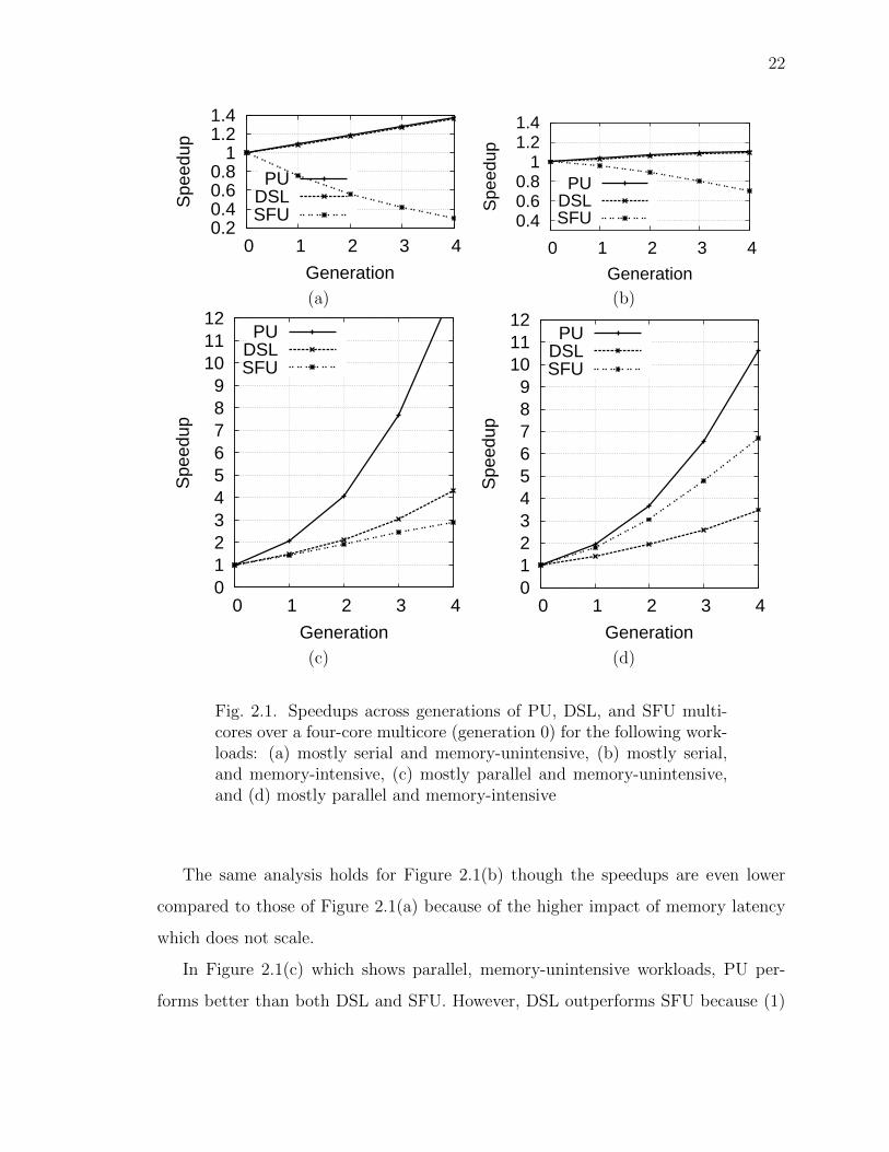
characteristics space in Figures 2.1(a) through (d), respectively: (1) mostly serial
21
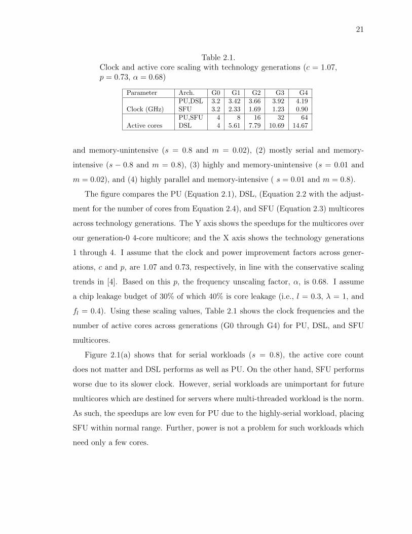
Table 2.1.Clock and active core scaling with technology generations (c = 1.07,p = 0.73, α = 0.68)
and memory-unintensive (s = 0.8 and m = 0.02), (2) mostly serial and memory-
intensive (s − 0.8 and m = 0.8), (3) highly and memory-unintensive (s = 0.01 and
m = 0.02), and (4) highly parallel and memory-intensive ( s = 0.01 and m = 0.8).
The figure compares the PU (Equation 2.1), DSL, (Equation 2.2 with the adjust-
ment for the number of cores from Equation 2.4), and SFU (Equation 2.3) multicores
across technology generations. The Y axis shows the speedups for the multicores over
our generation-0 4-core multicore; and the X axis shows the technology generations
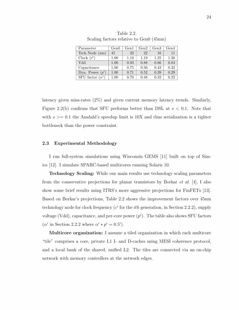
1 through 4. I assume that the clock and power improvement factors across gener-
ations, c and p, are 1.07 and 0.73, respectively, in line with the conservative scaling
trends in [4]. Based on this p, the frequency unscaling factor, α, is 0.68. I assume
a chip leakage budget of 30% of which 40% is core leakage (i.e., l = 0.3, λ = 1, and
fl = 0.4). Using these scaling values, Table 2.1 shows the clock frequencies and the
number of active cores across generations (G0 through G4) for PU, DSL, and SFU
multicores.
Figure 2.1(a) shows that for serial workloads (s = 0.8), the active core count
does not matter and DSL performs as well as PU. On the other hand, SFU performs
worse due to its slower clock. However, serial workloads are unimportant for future
multicores which are destined for servers where multi-threaded workload is the norm.
As such, the speedups are low even for PU due to the highly-serial workload, placing
SFU within normal range. Further, power is not a problem for such workloads which
need only a few cores.
22
0.2 0.4 0.6 0.8
1 1.2 1.4
0 1 2 3 4
Spe
edup
Generation
PUDSLSFU 0.4
0.6 0.8
1 1.2 1.4
0 1 2 3 4
Spe
edup
Generation
PUDSLSFU
(a) (b)
0 1 2 3 4 5 6 7 8 9
10 11 12
0 1 2 3 4
Spe
edup
Generation
PUDSLSFU
0 1 2 3 4 5 6 7 8 9
10 11 12
0 1 2 3 4
Spe
edup
Generation
PUDSLSFU
(c) (d)
Fig. 2.1. Speedups across generations of PU, DSL, and SFU multi-cores over a four-core multicore (generation 0) for the following work-loads: (a) mostly serial and memory-unintensive, (b) mostly serial,and memory-intensive, (c) mostly parallel and memory-unintensive,and (d) mostly parallel and memory-intensive
The same analysis holds for Figure 2.1(b) though the speedups are even lower
compared to those of Figure 2.1(a) because of the higher impact of memory latency
which does not scale.
In Figure 2.1(c) which shows parallel, memory-unintensive workloads, PU per-
forms better than both DSL and SFU. However, DSL outperforms SFU because (1)
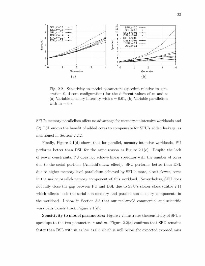
Fig. 2.2. Sensitivity to model parameters (speedup relative to gen-eration 0, 4-core configuration) for the different values of m and s:(a) Variable memory intensity with s = 0.01, (b) Variable parallelismwith m = 0.8
SFU’s memory parallelism offers no advantage for memory-unintensive worklaods and
(2) DSL enjoys the benefit of added cores to compensate for SFU’s added leakage, as
mentioned in Section 2.2.2.
Finally, Figure 2.1(d) shows that for parallel, memory-intensive workloads, PU
performs better than DSL for the same reason as Figure 2.1(c). Despite the lack
of power constraints, PU does not achieve linear speedups with the number of cores
due to the serial portions (Amdahl’s Law effect). SFU performs better than DSL
due to higher memory-level parallelism achieved by SFU’s more, albeit slower, cores
in the major parallel-memory component of this workload. Nevertheless, SFU does
not fully close the gap between PU and DSL due to SFU’s slower clock (Table 2.1)
which affects both the serial-non-memory and parallel-non-memory components in
the workload. I show in Section 3.5 that our real-world commercial and scientific
workloads closely track Figure 2.1(d).
Sensitivity to model parameters: Figure 2.2 illustrates the sensitivity of SFU’s
speedups to the two parameters s and m. Figure 2.2(a) confirms that SFU remains
faster than DSL with m as low as 0.5 which is well below the expected exposed miss
1 Number of cores (PU/SFU) 4 8 16 32 64 2X per gen2 Number of cores (DSL) 4 6 8 12 16 Power-limited3 Clock (GHz) (PU/DSL) 3.2 3.52 3.81 4 4.16 As per Table 2.24 Clock (GHz) (SFU) 3.2 2.48 1.73 1.28 0.89 As per Table 2.25 Shared L2 size (MB) 4 8 16 32 64 2X per gen6 Shared L2 banks 4 8 16 32 64 2X per gen7 Network 2x2 2x4 4x4 4x8 8x88 Link latency (cycles) 2 2 2 3 3 Slower than f scaling9 Memory (DSL/PU) cycles 320 344 368 380 400 2% reduction per gen10 Memory (SFU) cycles 320 240 180 124 86 2% reduction per gen11 Number of DRAM banks 16 32 64 128 256 2X per gen12 Number of memory channels 1 2 4 8 16 2X per gen13 Number of instances (DSL) 1 1 2 4 4 Problem size scaling14 Number of instances (SFU/PU) 1 1 2 4 8 Problem size scaling
27
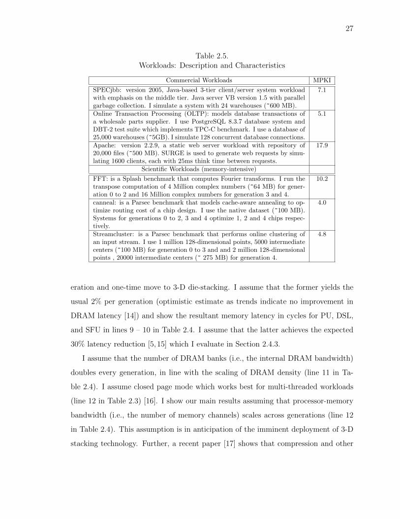
Table 2.5.Workloads: Description and Characteristics
Commercial Workloads MPKI
SPECjbb: version 2005, Java-based 3-tier client/server system workloadwith emphasis on the middle tier. Java server VB version 1.5 with parallelgarbage collection. I simulate a system with 24 warehouses (~600 MB).
7.1
Online Transaction Processing (OLTP): models database transactions ofa wholesale parts supplier. I use PostgreSQL 8.3.7 database system andDBT-2 test suite which implements TPC-C benchmark. I use a database of25,000 warehouses (~5GB). I simulate 128 concurrent database connections.
5.1
Apache: version 2.2.9, a static web server workload with repository of20,000 files (~500 MB). SURGE is used to generate web requests by simu-lating 1600 clients, each with 25ms think time between requests.
17.9
Scientific Workloads (memory-intensive)
FFT: is a Splash benchmark that computes Fourier transforms. I run thetranspose computation of 4 Million complex numbers (~64 MB) for gener-ation 0 to 2 and 16 Million complex numbers for generation 3 and 4.
10.2
canneal: is a Parsec benchmark that models cache-aware annealing to op-timize routing cost of a chip design. I use the native dataset (~100 MB).Systems for generations 0 to 2, 3 and 4 optimize 1, 2 and 4 chips respec-tively.
4.0
Streamcluster: is a Parsec benchmark that performs online clustering ofan input stream. I use 1 million 128-dimensional points, 5000 intermediatecenters (~100 MB) for generation 0 to 3 and and 2 million 128-dimensionalpoints , 20000 intermediate centers (~ 275 MB) for generation 4.
4.8
eration and one-time move to 3-D die-stacking. I assume that the former yields the
usual 2% per generation (optimistic estimate as trends indicate no improvement in
DRAM latency [14]) and show the resultant memory latency in cycles for PU, DSL,
and SFU in lines 9 – 10 in Table 2.4. I assume that the latter achieves the expected
30% latency reduction [5, 15] which I evaluate in Section 2.4.3.
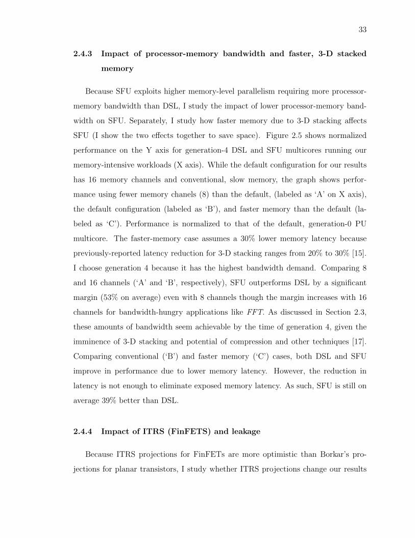
I assume that the number of DRAM banks (i.e., the internal DRAM bandwidth)
doubles every generation, in line with the scaling of DRAM density (line 11 in Ta-
ble 2.4). I assume closed page mode which works best for multi-threaded workloads
(line 12 in Table 2.3) [16]. I show our main results assuming that processor-memory
bandwidth (i.e., the number of memory channels) scales across generations (line 12
in Table 2.4). This assumption is in anticipation of the imminent deployment of 3-D
stacking technology. Further, a recent paper [17] shows that compression and other
28
techniques can allow conventional pin bandwidth to scale beyond 100 cores, covering
many future generations. Nevertheless, I include results constraining the number of
memory channels in Section 2.4.3.
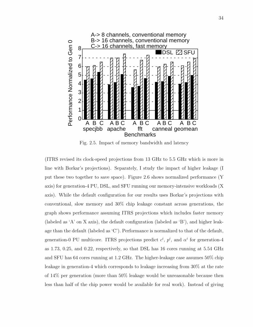
Leakage: As explained in Section 2.2.2, recent commercial microprocessors in-
crease transistor threshold voltages and decrease transistor speeds to hold leakage
at a constant 25-30% of the constant total power budget [10]. Consequently, the
total dynamic power budget is also a constant. Borkar’s conservative scaling, and
therefore Table 2.2, include the effects of such adjustments. While our main results
assume a chip leakage budget of 30% held constant across generations (i.e., l = 0.3
and λ = 1), I also show brief results for leakage growing from 30% to 50% across our
four generations (i.e., l = 0.3 and λ = 1.15). Based on our reasons in Section 2.2.2, I
assume that 40% of the chip leakage is in the cores (i.e., fl = 0.4).
Workloads: I run the commercial and scientific workloads shown in Table 3.4.
Note, because our focus is on memory-intensive workloads where SFU offers maximum
advantage, I focus on the above workloads. However, because it is important to show
that SFU does not hurt performance for memory-unintensive workloads, I show ad-
ditional results in Section 2.4.5 for three other workloads that are compute-intensive.
Recall from Section 2.2.2 that I revert to DSL for memory-unintensive (based on a
miss-rate threshold) workloads. To account for the general trend of data increasing
with cache sizes across generations, I scale up the workload size across generations so
that the off-chip miss rate, shown as misses per kilo instructions (MPKI) in Table 3.4,
remains about the same across generations. Because even higher miss rates would
give more opportunity for SFU over DSL, this constant miss rate is a conservative
choice. While the scientific workloads are amenable to easy scale-up by increasing
the datasets, meaningfully scaling up the commercial workloads’ datasets to 128 cores
requires significant amount of domain expertise to achieve realistic settings (e.g., tune
various benchmark parameters to avoid software bottlenecks). Instead, I scale up the
commercial workloads by consolidating multiple instances of the same benchmark as
shown in lines 13 – 14 of Table 2.4 (i.e., homogeneous consolidation as done in [18]).
29
This methodology is in line with the trend in software consolidation especially on large
multicores [18]. I compile our workloads with full software prefetching so that the
exposed memory latency is realistic. Finally, because OLTP runs are long-running,
I only include OLTP in the main results (Section 2.4.1 and Section 2.4.6). I omit
OLTP from the other sensitivity results.
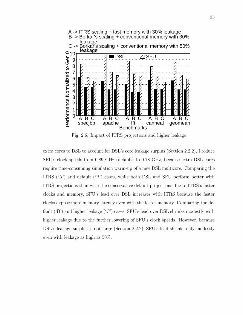
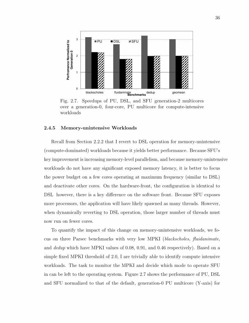
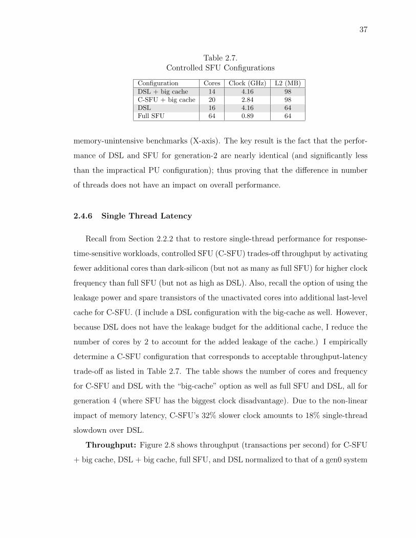
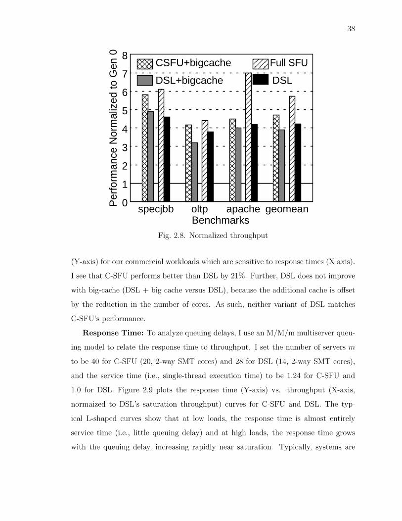
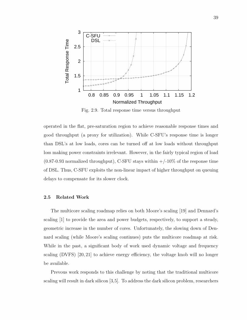
2.4 Experimental Results
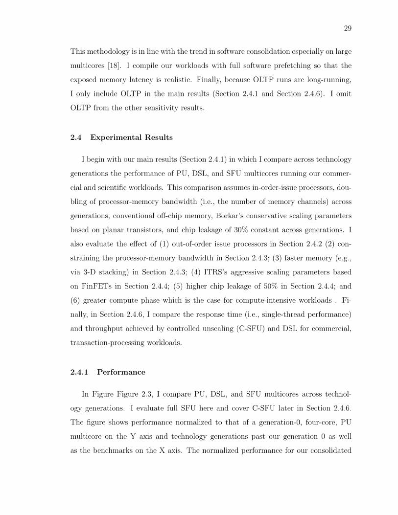
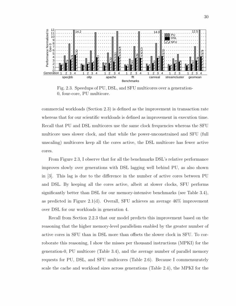
I begin with our main results (Section 2.4.1) in which I compare across technology
generations the performance of PU, DSL, and SFU multicores running our commer-
cial and scientific workloads. This comparison assumes in-order-issue processors, dou-
bling of processor-memory bandwidth (i.e., the number of memory channels) across
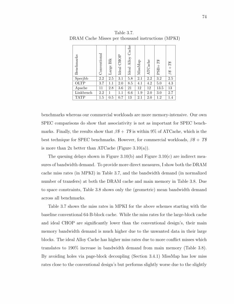
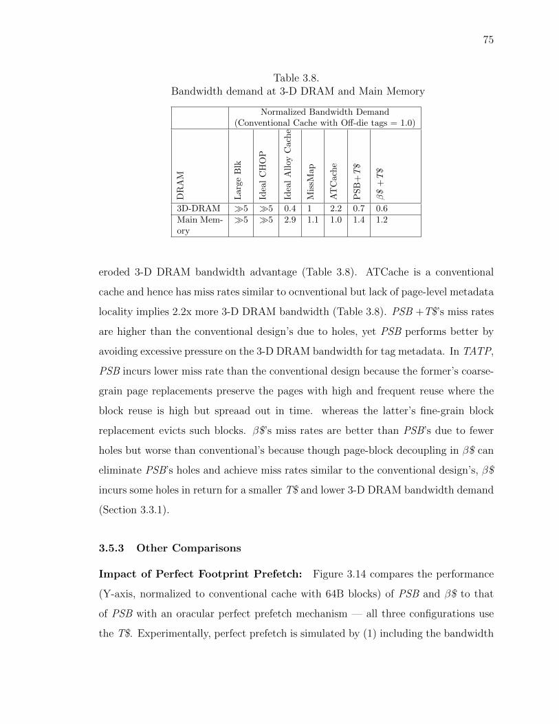
# of blocks evicted per page upon replacement in a PSB cache
Specjbb
OLTP
Apache
Linkbench
TATP
Fig. 3.4. Block density distribution
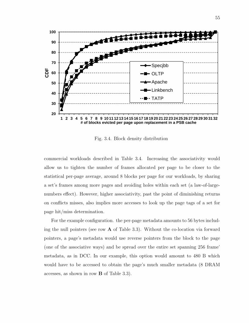
commercial workloads described in Table 3.4. Increasing the associativity would
allow us to tighten the number of frames allocated per page to be closer to the
statistical per-page average, around 8 blocks per page for our workloads, by sharing
a set’s frames among more pages and avoiding holes within each set (a law-of-large-
numbers effect). However, higher associativity, past the point of diminishing returns
on conflicts misses, also implies more accesses to look up the page tags of a set for
page hit/miss determination.
For the example configuration. the per-page metadata amounts to 56 bytes includ-
ing the null pointers (see row A of Table 3.3). Without the co-location via forward
pointers, a page’s metadata would use reverse pointers from the block to the page
(one of the associative ways) and be spread over the entire set spanning 256 frame’
metadata, as in DCC. In our example, this option would amount to 480 B which
would have to be accessed to obtain the page’s much smaller metadata (8 DRAM
accesses, as shown in row B of Table 3.3).
56
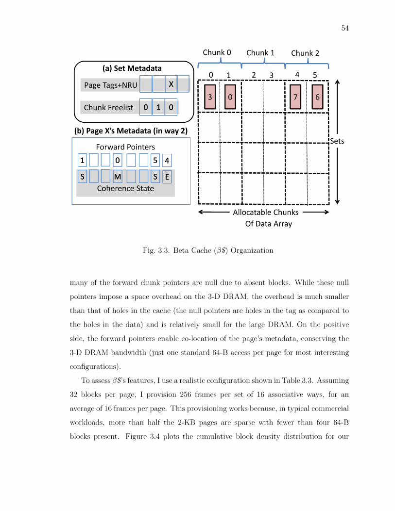
Chunks: Recall from Section 3.1 that the T$ uses reverse pointers to avoid β$’s
null-pointer overhead which is significant for the small T$. However, allocating space
at the granularity of only one block would imply a reverse pointer per block in the
T$ which still amounts to high space overhead. Therefore, β$ allocates space at the
chunk granularity (e.g., 4 blocks per chunk) upon a miss.
Accesses may miss in the page (i.e., the entire page is missing), or in a block of a
page that is present. A page miss results in the (full) eviction of a victim page and
the freeing of its chunks. Upon a block miss, β$ allocates a chunk either by reclaiming
a free chunk (from a previous eviction of a page which vacates all its chunks) or by
partially evicting a chunk of a page in the set if no chunk is free. In either case,
the page’s metadata records a forward pointer to the first frame within the allocated
chunk for the missing block, as shown by ”Page X’s Metadata” in Figure 3.3(b).
Once a chunk is allocated, the subsequent blocks are allocated within the chunk in
left-to-right order. For maximum flexibility in using the set’s space, the blocks of a
page may be located in any order and are discontiguous.
Chunking may cause a few holes in β$ (data array) due to internal fragmentation
but so significantly reduces the T$’s space overhead that the trade-off is justified. I
show an example of how much the overhead reduces in Section 3.3.2.
Per-set free lists: Upon a block miss, determining which, if any, chunks are free
requires examining the metadata of all the pages in the set which would incur many
3-D DRAM accesses. To alleviate this problem, I propose to maintain a free list per
set as a bit vector, as shown in ”Set Metadata” in Figure 3.3(a) (i.e., 64-bit vector
for our example of 64 chunks per set). Freeing of chunks upon full eviction results in
the corresponding free-list bits being set and allocation of chunks results in clearing
of the bits. Without the chunks, the free list would grow but may still fit within a
3-D DRAM access. However, this growth imposes significant space overhead on the
small T$, as I will see in Section 3.3.2.
57
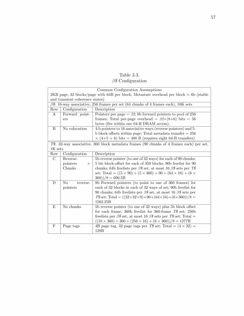
Table 3.3.β$ Configuration
Common Configuration Assumptions2KB page; 32 blocks/page with 64B per block; Metastate overhead per block = 6b (stableand transient coherence states)β$: 16-way associative, 256 frames per set (64 chunks of 4 frames each), 16K setsRow Configuration Description
A Forward point-ers
Pointers per page = 32; 8b forward pointers to pool of 256frames; Total per-page overhead = 32×(8+6) bits = 56bytes (fits within one 64-B DRAM access).
B No colocation 4-b pointers to 16 associative ways (reverse pointers) and 5-b block offsets within page; Total metadata transfer = 256× (4+5 + 6) bits = 480 B (requires eight 64-B transfers)
T$: 32-way associative, 360 block metadata frames (90 chunks of 4 frames each) per set,1K setsRow Configuration Description
C Reverse-pointers +Chunks
5b reverse pointer (to one of 32 ways) for each of 90 chunks;5 bit block-offset for each of 350 blocks; 90b freelist for 90chunks; 64b freelists per β$ set, at most 16 β$ sets per T$set; Total = ((5× 90) + (5× 360) + 90 + (64× 16) + (6×360))/8 = 690.5B
D No reverse-pointers
9b Forward pointers (to point to one of 360 frames) foreach of 32 blocks in each of 32 ways of set; 90b freelist for90 chunks; 64b freelists per β$ set, at most 16 β$ sets perT$ set; Total = ((32×32×9)+90+(64×16)+(6×360))/8 =1562.25B
E No chunks 5b reverse pointer (to one of 32 ways) plus 5b block offsetfor each frame; 360b freelist for 360-frame T$ set; 256bfreelists per β$ set, at most 16 β$ sets per T$ set; Total =((10× 360) + 360 + (256× 16) + (6× 360))/8 = 1277B
F Page tags 4B page tag, 32 page tags per T$ set; Total = (4× 32) =128B
58
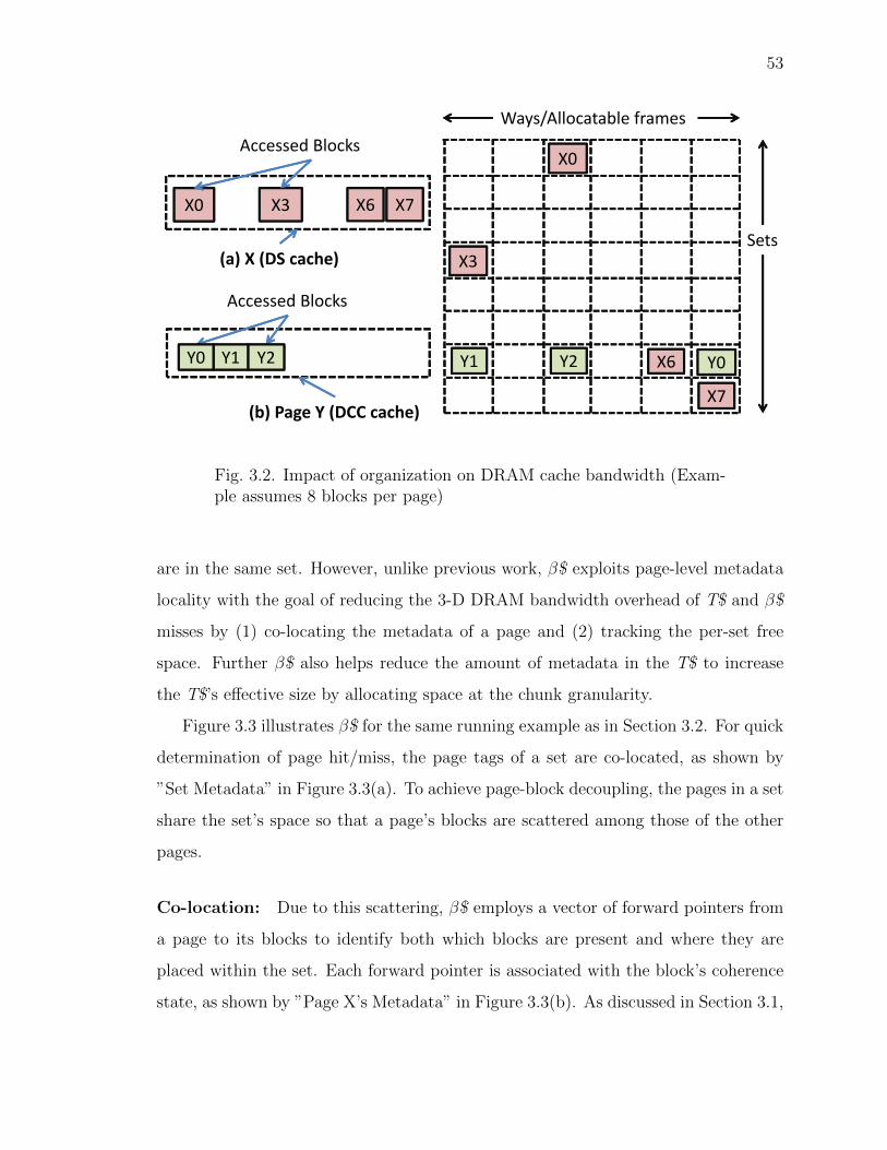
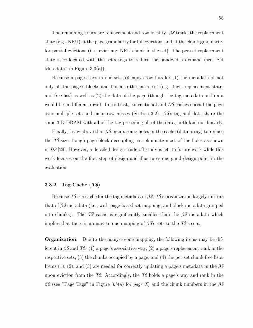
The remaining issues are replacement and row locality. β$ tracks the replacement
state (e.g., NRU) at the page granularity for full evictions and at the chunk granularity
for partial evictions (i.e., evict any NRU chunk in the set). The per-set replacement
state is co-located with the set’s tags to reduce the bandwidth demand (see ”Set
Metadata” in Figure 3.3(a)).
Because a page stays in one set, β$ enjoys row hits for (1) the metadata of not
only all the page’s blocks and but also the entire set (e.g., tags, replacement state,
and free list) as well as (2) the data of the page (though the tag metadata and data
would be in different rows). In contrast, conventional and DS caches spread the page
over multiple sets and incur row misses (Section 3.2). β$’s tag and data share the
same 3-D DRAM with all of the tag preceding all of the data, both laid out linearly.
Finally, I saw above that β$ incurs some holes in the cache (data array) to reduce
the T$ size though page-block decoupling can eliminate most of the holes as shown
in DS [29]. However, a detailed design trade-off study is left to future work while this
work focuses on the first step of design and illustrates one good design point in the
evaluation.
3.3.2 Tag Cache (T$)
Because T$ is a cache for the tag metadata in β$, T$’s organization largely mirrors
that of β$ metadata (i.e., with page-based set mapping, and block metadata grouped
into chunks). The T$ cache is significantly smaller than the β$ metadata which
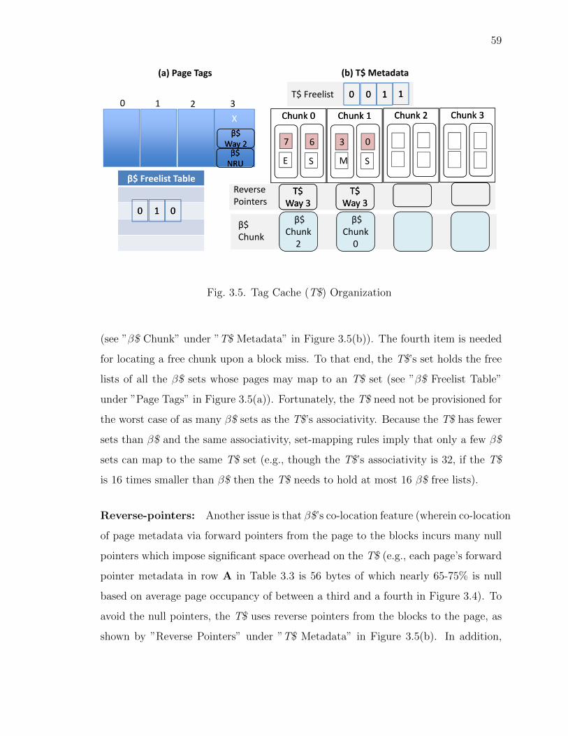
implies that there is a many-to-one mapping of β$’s sets to the T$’s sets.
Organization: Due to the many-to-one mapping, the following items may be dif-
ferent in β$ and T$: (1) a page’s associative way, (2) a page’s replacement rank in the
respective sets, (3) the chunks occupied by a page, and (4) the per-set chunk free lists.
Items (1), (2), and (3) are needed for correctly updating a page’s metadata in the β$
upon eviction from the T$. Accordingly, the T$ holds a page’s way and rank in the
β$ (see ”Page Tags” in Figure 3.5(a) for page X) and the chunk numbers in the β$
59
0 1 2
(a) Page Tags
X Chunk 1Chunk 1
3 0
M S
Chunk 2Chunk 2 Chunk 3Chunk 3
T$Way 3T$
Way 3T$
Way 3T$
Way 3
Chunk 0Chunk 0
67
E S
β$Chunk
2
β$Way 2β$
Way 2
Reverse Pointers
3
(b) T$ Metadata
β$NRUβ$NRU
β$Chunk
0
β$ Chunk
T$ Freelist
β$ Freelist Table
00 11 00
00 00 11 11
Fig. 3.5. Tag Cache (T$) Organization
(see ”β$ Chunk” under ”T$ Metadata” in Figure 3.5(b)). The fourth item is needed
for locating a free chunk upon a block miss. To that end, the T$’s set holds the free
lists of all the β$ sets whose pages may map to an T$ set (see ”β$ Freelist Table”
under ”Page Tags” in Figure 3.5(a)). Fortunately, the T$ need not be provisioned for
the worst case of as many β$ sets as the T$’s associativity. Because the T$ has fewer
sets than β$ and the same associativity, set-mapping rules imply that only a few β$
sets can map to the same T$ set (e.g., though the T$’s associativity is 32, if the T$
is 16 times smaller than β$ then the T$ needs to hold at most 16 β$ free lists).
Reverse-pointers: Another issue is that β$’s co-location feature (wherein co-location
of page metadata via forward pointers from the page to the blocks incurs many null
pointers which impose significant space overhead on the T$ (e.g., each page’s forward
pointer metadata in row A in Table 3.3 is 56 bytes of which nearly 65-75% is null
based on average page occupancy of between a third and a fourth in Figure 3.4). To
avoid the null pointers, the T$ uses reverse pointers from the blocks to the page, as
shown by ”Reverse Pointers” under ”T$ Metadata” in Figure 3.5(b). In addition,
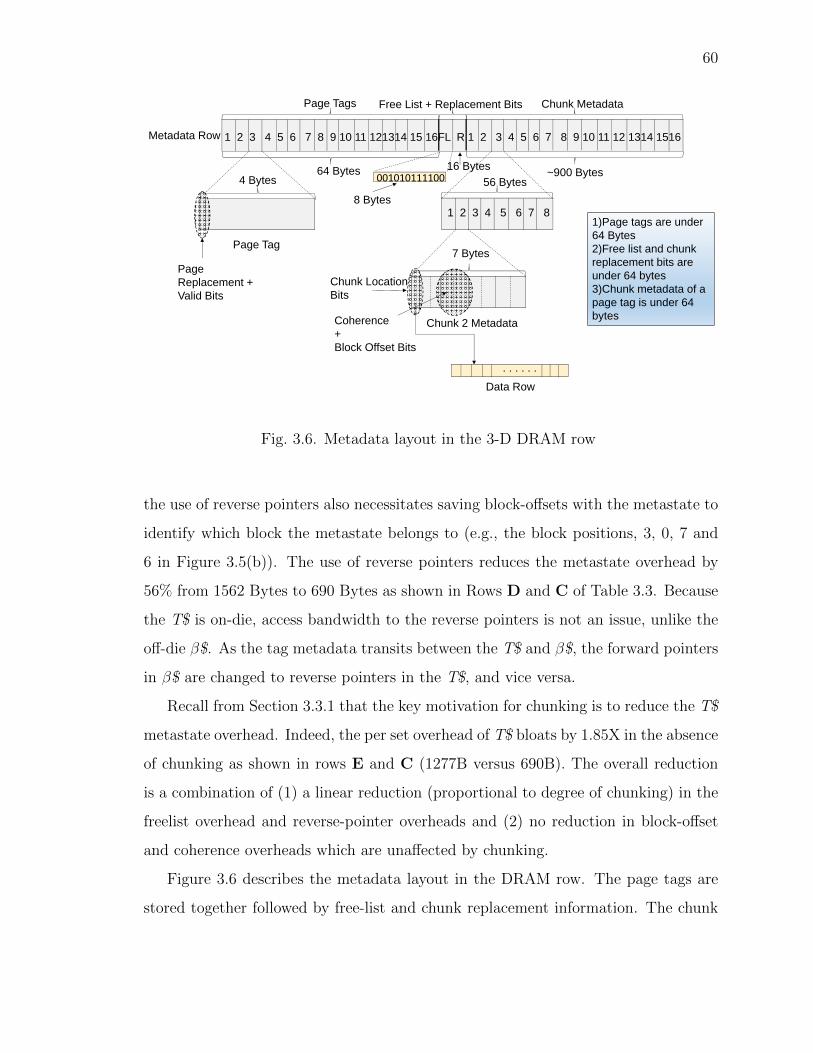
1)Page tags are under 64 Bytes2)Free list and chunk replacement bits are under 64 bytes3)Chunk metadata of a page tag is under 64 bytes
4 Bytes
. . . . . .
Data Row
Free List + Replacement Bits
001010111100
8 Bytes
16 Bytes
Fig. 3.6. Metadata layout in the 3-D DRAM row
the use of reverse pointers also necessitates saving block-offsets with the metastate to
identify which block the metastate belongs to (e.g., the block positions, 3, 0, 7 and
6 in Figure 3.5(b)). The use of reverse pointers reduces the metastate overhead by
56% from 1562 Bytes to 690 Bytes as shown in Rows D and C of Table 3.3. Because
the T$ is on-die, access bandwidth to the reverse pointers is not an issue, unlike the
off-die β$. As the tag metadata transits between the T$ and β$, the forward pointers
in β$ are changed to reverse pointers in the T$, and vice versa.
Recall from Section 3.3.1 that the key motivation for chunking is to reduce the T$
metastate overhead. Indeed, the per set overhead of T$ bloats by 1.85X in the absence
of chunking as shown in rows E and C (1277B versus 690B). The overall reduction
is a combination of (1) a linear reduction (proportional to degree of chunking) in the
freelist overhead and reverse-pointer overheads and (2) no reduction in block-offset
and coherence overheads which are unaffected by chunking.
Figure 3.6 describes the metadata layout in the DRAM row. The page tags are
stored together followed by free-list and chunk replacement information. The chunk
61
metadata associated to each page tag is laid out at the end. It is important to note
that all page tags, the free-list and chunk replacement bits, and chunk metadata
for the matching page tag (or victim page tag) can be transferred in 3 memory
transactions. Great care is taken to ensure that the metadata layout is done in a
way that minimizes the number of memory transactions needed to fetch the required
metadata.
Operation: The T$ and the metadata in the β$ operates like a traditional 2-level
hierarchy wherein addresses are first looked up in the T$ before accessing the β$ (in
case of a miss in the T$). Because of the two-level organization, each access can face
one of four possible outcomes (hit/miss in the T$, hit/miss in the β$). The number
of DRAM accesses for each of these four cases is summarized in Table 3.2. Note, not
all cases are equally likely; hits are common and misses are uncommon in each of the
two levels. Later, in Section 3.5.1, I show that β$ + T$ reduces the total number of
transfers from 3D-DRAM.
A key invariant I enforce in the T$’s operation is that for the pages present in
the T$, the block information in the T$ is the same as that in the β$. That is, the
T$ maintains full and current information about a page. This invariant guarantees
that for any given access, a page hit in the T$ ensures that the block hit (miss) in
the T$ is a hit (miss) in the β$ as well. The rationale for this invariant is that (1) it
prevents unnecessary accesses to the β$, and (2) it matches the T$’s goal of exploiting
page-level spatial locality by fetching (and maintaining) full page information.
As with any tag-caching scheme, the T$ requires page metadata invalidations
whenever a page is evicted from the underlying cache (β$, in our case). Further,
to enforce the invariant, I require one additional safeguard – in the case of partial
replacement of a chunk of a page, the update must be actively propagated to the
corresponding page entry in the T$ to ensure that the metadata of the victim chunk
is also evicted from the T$.
62
For example, eviction of a page results in the tag-cache entry being similarly
evicted from the T$.
Accordingly, accesses to the T$ and β$ fall into four cases (in increasing order of
difficulty): page hit and block hit (in both the T$ and β$), page hit (in the T$) and
block miss (in the β$), page miss in the T$ and block hit in the β$, page miss in the
T$ and block miss in the β$.
First case: In the first case, the metadata is served completely from the T$
without requiring any access to the 3-D DRAM. In the T$, the way pointers of all
the chunks in the indexed set are matched to identify the relevant chunks (e.g., 4-bit
way pointers of 64 chunks). Then the offsets of the matching chunks are searched to
identify the relevant block. This matching can be simplified to a few sequential steps
involving fewer matches per step (e.g., 4 groups of 16 chunks each). Such grouping
costs only a few cycles compared to the 3-D DRAM data access of more than 50
cycles.
Second case: In the second case, if space is already available in a chunk that is
not full (sub-case 1), the pre-allocated space is assigned to the block. If there is no
free space in existing chunks (sub-case 2), a new chunk, preferably a free chunk, is
allocated in both the T$ and β$. If there were no free lists, locating the free chunks
would incur many 3-D DRAM accesses to search through the forward pointers of
all the pages in the set (e.g., 8 64-B accesses each of which covers 2 pages’ forward
pointers shown in row A of Table 3.3). If no free chunks are available in the T$ and
β$ (sub-case 3), then a partial eviction occurs from the β$ (i.e., only one chunk is
evicted) and a full eviction from the T$ (i.e., a full page is evicted); recall that there
are no partial evictions , based on the replacement state for the respective sets in the
T$ and β$; from the T$. The partial β$ eviction incurs a 3-D DRAM read of the
coherence state in the β$ possibly followed by a writeback of the partially evicted
data to main memory and an update of the victim page’s block metadata (typically
two 3-D DRAM accesses). The T$ full eviction (in sub-case 3) incurs a reverse-to-
forward-converted metadata writeback to the β$ (typically one DRAM access for the
63
page’s tag and replacement state, another access for the page’s co-located metadata,
and one more for updating the free list vector). If the page’s metadata were not co-
located, the writeback would incur many 3-D DRAM accesses (e.g., 6 64-B accesses
for the page’s metadata scattered across the set as shown in row C of Table 3.3).
While the writeback can be reduced with metadata dirty bits, replacement state and
block occupancy often change and make the dirty bits ineffective (our implementation
does not use metadata dirty bits).
Irrespective of the sub-case (i.e., presence or absence of free chunks), the second
case is a block miss in the β$ which requires a fill of the data from main memory
into the DRAM cache. Assuming the β$ (and T$) is provisioned appropriately with
enough chunks, free chunks would be available in the common case. As such, the
first two cases (both page hits) correspond to the prevalent page-level spatial locality
and therefore capture a majority of accesses (e.g., 80%) most of which require only
a few or no 3-D DRAM accesses. Table 3.2 briefly summarizes the number of 3-D
DRAM accesses for the two cases (rows ”Hit/Hit” and ”Hit/Miss”). While full/partial
evictions from the T$ and β$ are uncommon in the second case, they do occur in the
fourth case below where β$’s mechanisms of chunking, co-location and free lists are
more important.
Third case: In the third case of page miss in the T$ and block hit in the β$, there
are typically two 3-D DRAM accesses for the block hit: one to read the page tags of
the set in the β$ and another to read the co-located per-page metadata. Recall that
in a set in the β$, the page tags are co-located for quick page hit/miss determination.
In addition, the page miss in the T$ requires a full eviction from the T$ incurring a
metadata writeback to the β$ (like the second case above) and a page metadata fill
via a forward-to–reverse conversion (see ”Miss/Hit” row in Table 3.2; the transfers
may increase in case of dirty evictions). This case is uncommon as it corresponds to
the page being absent in the T$ but being present in the β$ which would not occur
often in the presence of page-level locality and a well-provisioned T$.
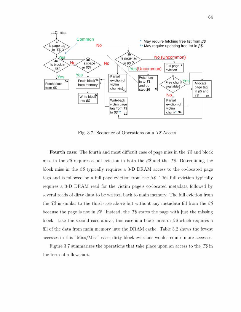
64
Yes
Is page tag in T$ ?
1
Is block inβ$?
2a
YesFetch block from β$
3a
No (Uncommon)
Full page eviction
Free chunk available?
7
8
No
Is page tag in β$ ?
2b
Fetch tag in to T$ and do step 10
Yes(Uncommon)
6
Fetch block from memory
Write blockInto β$
4a
5
Yes
No Is space in β$?
3bNo
Partialeviction of victim chunk(s)4b
Yes
NoPartialeviction of victim chunk*
Allocatepage tag in β$ andT$
9a
9b
LLC miss
* May require fetching free list from β$** May require updating free list in β$
Writebackvictim page tag from T$to β$ ** 10
Common
Fig. 3.7. Sequence of Operations on a T$ Access
Fourth case: The fourth and most difficult case of page miss in the T$ and block
miss in the β$ requires a full eviction in both the β$ and the T$. Determining the
block miss in the β$ typically requires a 3-D DRAM access to the co-located page
tags and is followed by a full page eviction from the β$. This full eviction typically
requires a 3-D DRAM read for the victim page’s co-located metadata followed by
several reads of dirty data to be written back to main memory. The full eviction from
the T$ is similar to the third case above but without any metadata fill from the β$
because the page is not in β$. Instead, the T$ starts the page with just the missing
block. Like the second case above, this case is a block miss in β$ which requires a
fill of the data from main memory into the DRAM cache. Table 3.2 shows the fewest
accesses in this ”Miss/Miss” case; dirty block evictions would require more accesses.
Figure 3.7 summarizes the operations that take place upon an access to the T$ in
the form of a flowchart.
65
Table 3.4.Benchmarks
Benchmark Description Memory Foot-print (GB)
Specjbb: version 2005, Java-based 3-tier client/server system workload with emphasis onthe middle tier. Java server VB version 1.5 with parallel garbage collection. I simulate2 JVMs each hosting 24 warehouses. I warmup the benchmark for 180,000 transactionsand measure performance for 2,000 transactions
1.2
Online Transaction Processing (OLTP): models database transactions of a wholesaleparts supplier. I use PostgreSQL 8.3.7 database system and DBT-2 test suite whichimplements TPC-C benchmark. I reduced number of items and districts per warehouseand customers per district to allow a larger number of warehouses. I use 8 databases eachwith 25,000 warehouses. I simulate 128 concurrent database connections per database. Iwarmup the databases for 80,000 transactions each before taking measurements for 200transactions
64
Apache: version 2.2.9, a static web server workload. I use 8 webservers hosting a 160,000files. SURGE is used to generate web requests by simulating 12800 clients, each with25ms think time between requests. I warmup the webservers for 1,000,000 transactionseach before taking measurements for 1,000 transactions
4
Linkbench: models database queries to a social graph e.g Facebook. I use MySQL 5.6.14database system and the Linkbench social graph and query generator. I use 8 databaseseach with 5 million keys. I configure MySQL with a 4 GB buffer pool and InnoDBstorage engine. I generate the social graph, load the keys, warmup the databases for300,000 transactions, and perform our measurements for 500 transactions
48
Telecom Application Transaction Processing (TATP): models database transactions of aHome Location Register (HLR) database used by a mobile carrier. I use MySQL 5.6.14database system and OLTP-Bench which implements the request generator in java. Iuse 8 databases each with a scale factor of 40. I use 40 client terminals and defaultweights. Each MySQL database is configured with an 4 GB buffer pool and InnoDBstorage engine. I warmup the database for 300,000 transactions and take measurementsfor 500 transactions
40
Spec2006: I evaluate 4 spec programs (astar,omnetpp,mcf,libquantum) in rated mode (8copies each). I use simpoints to identify a simulation interval. I warmup the caches for250 million instructions and do measuremeants for 100 million instructions
Die-stacked DRAM (256 MB)Bus frequency 1.6 GHzChannels 4Ranks 1 per channelBanks 8 per rankBus width 128 bits per channeltCAS-tRP-tRCD-tRAS 9-9-9-27
Main Memory (64 GB)Bus frequency 800 MHzChannels 2Ranks 1 per channelBanks 8 per rankRow buffer size 2KBBus width 64 Bits per channeltCAS-tRP-tRCD-tRAS 11-11-11-33
the bus speed, and twice the bus-width as main memory. Other timing parameters
for the 3-D DRAM and main memory are shown in Table 3.5; the DRAM has 5x
more bandwidth than memory (2x more banks and 2.5x shorter bank occupancy, as
discussed in Section 3.2). Recall, the β$ and T$ parameters are shown in Table 3.3. I
determine the associativity of the conventional DRAM cache empirically. As shown in
Figure 3.8, commercial workloads see significant performance improvements as asso-
ciativity (X-axis) increases up to 16. However, the impact of associativity in spec2006
programs is insignificant. For the commercial workloads, increasing the associativity
beyond 16 resulted in insignificant performance gains. As such, all our experiments
use a 16-way associative DRAM cache.
68
Table 3.6.Tag Overhead (MB)
Com
pon
ents
Conve
nti
on
al
DS
Larg
eB
lk
Idea
lC
HO
P
Idea
lA
lloy
Mis
sMap
PS
B
β$
Totalfor256-MB
17.5 10.2 0.5 0.5 16 17.5 3.5 15
Totalfor1-GB
70 40 2.1 2.1 64 70 14 60
Totalfor4-GB
280 160 8.5 8.5 256 280 56 240
Comparison with other cache organizations I compare the following schemes:
(1) a conventional cache using large, 2-KB blocks; (2) an ideal version of CHOP [27]
using 2-KB blocks with an experimentally determined migration threshold of 8 ac-
cesses, and an unbounded filter-cache to filter sparse pages without any loss of history;
(3) an ideal Alloy cache using 64-B blocks with the tag metadata in the 3-D DRAM
and perfect hit-miss prediction [26]; (4) MissMap with compound accesses to the tag
metadata and data which are stored in the 3-D DRAM [25]; and (5) a PSB cache
using 2-KB pages and 64-B blocks with tag metadata in DRAM cache and a T$
for caching the tag metadata; and (6) a β$ cache and a T$ using 2-KB pages, 64-B
blocks, and 4-block chunks. I model the bus and 3-D DRAM bank occupancy of
non-critical-path events such as writeback of coherence and replacement state for all
the caches, as these events impact the bandwidth demand on the 3-D DRAM, as
discussed in Section 3.2.
3.4.1 Tag Overhead
Varying the DRAM cache size as 256 MB, 1 GB, and 4 GB, Table 3.6 shows
the total tag overhead conventional 64-B-block cache, DS, conventional 2-KB-block
69
0
5
10
15
20
25
30
35
40
45
Specjbb OLTP Apache Linkbench TATP
Mis
s ra
tio (l
ower
is b
ette
r)
Benchmarks
3D-cache (256MB)T$ (512 sets)
T$ (1K sets)
T$ (2K sets)
Fig. 3.9. T$ miss rate
caches (Large Blk in table), ideal 2-KB-block CHOP [27], MissMap [25], ideal Alloy
cache [26], PSB, and β$. The ideal variants are described in Section 3.4. The overhead
includes tags, replacement state (NRU bits at the appropriate granularity), sub-block
pointers or presence bit vectors (for β$ and PSB), per-block coherence state, reverse
(block-to-page) pointers (for DS) and free-lists (for β$). Excluding the large-block
variants, the metastate for all other techniques is too large to include on the processor
die. As such, our performance comparisons configure these schemes to use a tag cache
to hold a subset of the total metadata on the processor die.
In Figure 3.9, I show the T$’s page miss rate for our benchmarks as I vary its
size as 512, 1K (default),and 2K sets (410, 820, and 1640 KB in total size), which
are 30x, 15x, and 7.5x fewer than the DRAM cache’s sets. I also show the 256-MB
DRAM cache’s block miss rate for reference. While the T$’s page miss rate lowers
as expected with its size, the more important point is that the T$’s page miss rate is
70
far better than the DRAM cache’s block miss rate highlighting the key role of spatial
locality in DRAM cache design.
3.5 Results
I compare the performance of β$ + T$ against several previous schemes. I first
show that β$ + T$ outperforms the competition because of improved bandwidth
efficiency. I then show that omitting β$’s features results in increased bandwidth
demand and hence lower performance. Finally, I show some results for sensitivity to
3-D DRAM bandwidth.
3.5.1 Performance
In Figure 3.10(a), I compare the performance of a conventional 2-KB-block cache
benchmarks whereas our commercial workloads are more memory-intensive. Our own
SPEC comparisons do show that associativity is not as important for SPEC bench-
marks. Finally, the results show that β$ + T$ is within 9% of ATCache, which is the
best technique for SPEC benchmarks. However, for commercial workloads, β$ + T$
is more than 2x better than ATCache (Figure 3.10(a)).
The queuing delays shown in Figure 3.10(b) and Figure 3.10(c) are indirect mea-
sures of bandwidth demand. To provide more direct measures, I show both the DRAM
cache miss rates (in MPKI) in Table 3.7, and the bandwidth demand (in normalized
number of transfers) at both the DRAM cache and main memory in Table 3.8. Due
to space constraints, Table 3.8 shows only the (geometric) mean bandwidth demand
across all benchmarks.
Table 3.7 shows the miss rates in MPKI for the above schemes starting with the
baseline conventional 64-B-block cache. While the miss rates for the large-block cache
and ideal CHOP are significantly lower than the conventional design’s, their main
memory bandwidth demand is much higher due to the unwanted data in their large
blocks. The ideal Alloy Cache has higher miss rates due to more conflict misses which
translates to 190% increase in bandwidth demand from main memory (Table 3.8).
By avoiding holes via page-block decoupling (Section 3.4.1) MissMap has low miss
rates close to the conventional design’s but performs slightly worse due to the slightly
75
Table 3.8.Bandwidth demand at 3-D DRAM and Main Memory
Normalized Bandwidth Demand(Conventional Cache with Off-die tags = 1.0)
DR
AM
Lar
ge
Blk
Idea
lC
HO
P
Idea
lA
lloy
Cac
he
Mis
sMap
AT
Cac
he
PS
B+T$
β$
+T$
3D-DRAM �5 �5 0.4 1 2.2 0.7 0.6Main Mem-ory
�5 �5 2.9 1.1 1.0 1.4 1.2
eroded 3-D DRAM bandwidth advantage (Table 3.8). ATCache is a conventional
cache and hence has miss rates similar to ocnventional but lack of page-level metadata
locality implies 2.2x more 3-D DRAM bandwidth (Table 3.8). PSB +T$’s miss rates
are higher than the conventional design’s due to holes, yet PSB performs better by
avoiding excessive pressure on the 3-D DRAM bandwidth for tag metadata. In TATP,
PSB incurs lower miss rate than the conventional design because the former’s coarse-
grain page replacements preserve the pages with high and frequent reuse where the
block reuse is high but spreaad out in time. whereas the latter’s fine-grain block
replacement evicts such blocks. β$’s miss rates are better than PSB’s due to fewer
holes but worse than conventional’s because though page-block decoupling in β$ can
eliminate PSB’s holes and achieve miss rates similar to the conventional design’s, β$
incurs some holes in return for a smaller T$ and lower 3-D DRAM bandwidth demand
(Section 3.3.1).
3.5.3 Other Comparisons
Impact of Perfect Footprint Prefetch: Figure 3.14 compares the performance
(Y-axis, normalized to conventional cache with 64B blocks) of PSB and β$ to that
of PSB with an oracular perfect prefetch mechanism — all three configurations use
the T$. Experimentally, perfect prefetch is simulated by (1) including the bandwidth
76
0
0.2
0.4
0.6
0.8
1
1.2
1.4
1.6
Specjbb OLTP Apache Linkbench TATP Geomean
Per
form
ance
Nor
mal
ized
to
Con
vent
iona
l Cac
he w
ith O
ff-di
e ta
gs
Benchmarks
PSB with T$ PSB with T$ and Perfect Footprint Predictor β$+T$
Fig. 3.14. Perfect Footprint Prefetch
cost (bank occupancy) of the subset of blocks of a page that are accessed before page
replacement, and (2) considering any page hit to be a block hit. The addition of
perfect footprint prefetching offers a modest improvement over PSB + T$; β$ +T$
remains significantly better without any prefetching at all. This result is not surprising
because the problem is one of bandwidth and not latency and prefetching improves
latency but not bandwidth (Section 3.2.4).
Impact isolation and comparison with DCC: Recall that two of our features
(colocation, free-lists) serve to minimize transfers from the DRAM cache and two of
them (chunking and reverse pointers) to reduce the size of the T$. The impact of
omitting the latter two features was previously isolated in Section 3.3.2 and Table 3.3;
the per-set state is reduced by more than 1.85X as a result. As such, I focus on the
impact of the former two features in this section.
To isolate the impact of β$’s features, Figure 3.15 shows the performance of β$
with and without the features (both variants use the T$). Without the features,
β$ defaults to a decoupled cache with set mapping at the page granularity (i.e.,
few holes), similar to DCC [34]. In such an organization, the metadata is scattered
77
0
0.2
0.4
0.6
0.8
1
1.2
Specjbb OLTP Apache Linkbench TATP Geomean
Perf
orm
ance
Nor
mal
ized
to β
$+T$
(hig
her i
s be
tter)
Benchmarks
Without colocation and freeliststWith colocation and freelists
Fig. 3.15. Impact of β$’s features and comparison with DCC
across the set, which destroys metadata locality at the page-level. Consequently,
β$ loses significant performance despite using the T$ because the lack of page-level
metadata spatial locality results in many more 3-D DRAM accessses than the full β$
(Section 3.3.1). Thus, both T$ and β$’s features are needed for good performance.
Note, the above comparison is equivalent to a comparison of β$ +T$ with DCC+T$.
3.5.4 Sensitivity to 3-D DRAM bandwidth
Figure 3.16 shows the normalized performance (mean across all benchmarks, Y-
axis) of three systems (conventional with 64B blocks and off-die tags, PSB +T$, and
β$ + T$) while varying 3-D DRAM bandwidth between 4X and 6X of main memory
bandwidth. (Recall that our main results assume 3-D DRAM has 5X the bandwidth
of main memory. I use the conventional cache with 64B blocks and off-die tags and
5X bandwidth as our normalization baseline.)
When available bandwidth is reduced (see 4X bars in Figure 3.16, 3-D bandwidth
becomes a more precious resource. This results in β$ +T$ widening its performance
gap relative to both PSB + T$ and conventional cache. In contrast, when I increase
78
00.20.40.60.8
11.21.4
4x 3D BW 5x 3D BW 6x 3D BW
Per
form
ance
Nor
mal
ized
to
Con
vent
iona
l Cac
he w
ith 5
x 3D
BW
and
Off-
die
Tags
Geomean
Conventional off-die tags PSB with T$ B$+T$
Fig. 3.16. Sensitivity to 3-D DRAM bandwidth
the bandwidth to 6X, the conventional cache, which is starved for 3-D bandwidth,
benefits significantly relative to β$ + T$. This is not surpising as abundant bandwidth
reduces the benefit of bandwidth efficiency that β$ enjoys. Interestingly, PSB + T$,
which is not limited by 3-D DRAM bandwidth, becomes worse than both conventional
and β$ +T$ configurations. The abundant bandwidth neutralizes any bandwidth
efficiency advantage PSB +T$ may have with respect to the conventional cache; and
PSB’s holes ensures that it has a disadvantage relative to both β$ and the conventional
cache.
3.6 Related work
Off-chip memory bandwidth has been predicted to be a limiting factor even before
the multicore era began [37]. While memory latency has always been a roadblock to
maximizing processor performance, the advent of multicores meant that the memory
subsystem will face another roadblock in the form of higher bandwidth demand. Not
as harsh as the memory latency wall – a name given to the ever-increasing diverg-
ing gap between the speed of operation of the processor and memory – designing
multicores with memory subsystem capable of sustaining the memory bandwidth de-
79
mand has its own challenges. Because die areas are not supposed to increase a lot
with smaller process nodes, the available physical space along the chip edges doesn’t
increase. Consequently, this makes it harder to increase the pin count as memory
traffic increases due to increase in core count. It is precisely for this reason pin-
bandwidth has been identified to be a major bottleneck for future multicores [38].
3-D die-stacking is the industry’s response to the pin-bandwidth problem [15, 24].
3-D die-stacking packages the on-chip logic and DRAM together albeit on different
dies. Through the use of TSVs, the 3-D DRAM is stacked on top of processors. An-
other form of packaging, 2.5-D packaging, instead of TSVs makes use of high density
interconnects between heterogeneous dies on a single package. As of now, it isn’t
clear which of the two packaging techniques will become more prevalent in the com-
ing years. However, it is fair to say that on-chip logic and DRAM will be packaged
together to serve the bandwidth demands of multicore. The idea of a tag cache has
been proposed before for off-chip DRAM sector cache [31]. While sector caches cap-
ture spatial locality very well without increasing metadata storage overhead, they
suffer from capacity loss due to holes incurred since page-level spatial locality varies.
I compare with this design point in my evaluation. [39] proposes a sector cache with
tags in 3-D, which on top of footprint prediction [32,33], uses way prediction to avoid
the tag lookup latency overhead if the tags are stored in 3-D cache. [39] operates
under the assumption that (1) 3-D bandwidth is plentiful (2) the loss of capacity due
to holes is a non-issue. First, while it is true that 3-D bandwidth is more than main
memory bandwidth, it is overly far-fetched to assume that such bandwidth would
justify wasting it in metadata lookup and updates. Architects will try to utilize the
copious bandwidth by increasing the core count, multithreading, or through other
means. Second, while the spatial locality exhibited by scaleout workloads may be
regular and plentiful, it is more varying for commercial workloads (Figure 3.4) where
the loss of capacity in the form of holes hurts MPKI. In contrast, β$ tries to minimize
loss of capacity due to holes by decoupling tagging granularity and allocation granu-
80
larity, and ensuring that bandwidth is not worsened due to the additional metadata
accesses through compact metadata layout techniques.
81
4. CONCLUSIONS
In this thesis, I have addressed the two fundamental problems that act as hindrance
for multi-core performance scaling: power and off-chip memory bandwidth.
Multi-cores are becoming increasingly power-contrained. The slowing of Den-
nard’s scaling, despite transistor innovations, is making it harder to get the desired
power savings transistor scaling has traditionally offered. Researchers have responded
to the slowing of Dennard’s scaling by arguing that dark silicon inevitably imposes a
performance limit and by advocating for customization to harness more performance
with the same power budget. While the DSL suggests an undesirable bound on per-
formance because of dark silicon, customization places multi-cores on a potentially
arduous path of considerable design/programmability cost. In chapter 2, I showed
that previously shown dark-silicon induced bounds on multi-core performance can be
surpassed, and that a gentler, evolutionary path for multi-cores exists. This path,
called successive frequency unscaling (SFU), involves successively scaling down the
clock frequency with each technology generation. SFU is based on the insights that
(1) frequency unscaling lowers per-core power where voltage-frequency scaling is in-
feasible, enabling more cores to be activated than the DSL approach; and (2) typical
multi-core workloads are memory-bound and benefit from the increased memory-level
parallelism achieved by the higher active core count. Guided by these insights and a
simple analytical model, SFU exploits two non-linearities: (1) the sub-linear impact
of clock speed on performance for memory-bound workloads and (2) the super-linear
impact of throughput on queuing delays. The first non-linearity implies that SFU’s
increased memory-level parallelism more than offsets the slower clock so that for
memory-intensive workloads, full SFU, where all the cores are powered up, performs
46% better than the DSL limit at the 11 nm technology node (18% better with out-of-
82
order cores). The second non-linearity comes into play for enterprise workloads where
both throughput and response times are important and full SFU’s aggressive clock
slowdown may penalize response times. To address this issue, I proposed controlled
SFU (C-SFU) which moderately slows down the clock and powers many, but not all,
cores to achieve 21% better throughput than the DSL limit at the 11 nm technol-
ogy node. The higher throughput non-linearly reduces queuing delays and thereby
compensates for the slower clock, resulting in C-SFU’s total response latency to be
within +/- 10% of that of DSL.
Finally, SFU’s simplicity enables a viable, evolutionary path of higher performance
for multi-cores at virtually no design effort or complexity.
On the memory bandwidth front, increasing the pin-bandwidth has become harder
due to the physical space limitations along the chip edges. While die sizes can be
increased to allow greater number of pins, doing so will increase the cost per chip
due to lower yield. Fortunately, the problem of memory bandwidth can be alleviated
by die-stacking of DRAM on the processor die which promises to continue scaling
the pin bandwidth to off-chip memory. The 3-D DRAM is expected to be used as a
large cache, which poses a choice between placing its large tag on the processor die
versus in the 3-D DRAM. Tag caching can strike a compromise between these choices
but fundamentally requires exploiting page-level metadata locality to ensure efficient
use of 3-D DRAM bandwidth. This locality crucially depends on the DRAM cache
and tag cache (T$) organizations. While plain sub-blocking exploits this locality but
incurs holes in the cache due to absent blocks, decoupled organizations avoid holes
but destroy this locality. In chapter 3, I proposed Bandwidth-Efficient Tag Access
(BETA) DRAM cache (β$) which both avoids holes and exploits the locality via its
four features. β$ targets two goals: (1) reducing the 3-D DRAM bandwidth cost of
T$ misses and DRAM cache misses, and (2) improving the T$’s effective size. For
the first goal, β$ exploits page-level metadata locality by (a) co-locating the meta-
data of a page, and (b) tracking the per-set free space. For the second goal, both
β$ and T$ reduce the amount of on-die metadata by (a) dynamically switching from
83
β$’s forward pointers to reverse pointers in the T$ at the β$-T$ interface, and (b)
allocating space in β$ at the chunk granularity. Using simulations, I conclusively
showed that (1) the primary concern in DRAM caches is bandwidth and not latency;
(2) previous proposals incur bandwidth bottlenecks at either main memory or 3-D
DRAM; (3) β$ with a T$ performs 15% better than the best previous scheme with a
similarly-sized T$; and (4) β$’s improvements are due to its tag bandwidth efficiency.
As die stacking is increasingly adopted, β$’s tag bandwidth efficiency will be a key
advantage over the other cache organizations.
While multi-cores do face challenges in delivering the promise of Moore’s law, this
thesis makes an attempt to show that multi-core performance can scale (for atleast a
decade) without a drastic paradigm shift in computing.
REFERENCES
84
REFERENCES
[1] R. Dennard, F. Gaensslen, V. Rideout, E. Bassous, and A. LeBlanc, “Designof ion-implanted mosfet’s with very small physical dimensions,” Solid-State Cir-cuits, IEEE Journal of, vol. 9, no. 5, pp. 256–268, 1974.
[2] “ARM-CTO: Power Surge could create ’Dark Silicon’http://www.eetimes.com/electronics-news/4085396/ARM-CTO-power-surge-could-create-dark-silicon-.”
[3] H. Esmaeilzadeh, E. Blem, R. St. Amant, K. Sankaralingam, and D. Burger,“Dark silicon and the end of multicore scaling,” in Proceeding of the ISCA-38,2011, pp. 365–376.
[4] S. Borkar and A. A. Chien, “The future of microprocessors,” Communicationsof the ACM, vol. 54, pp. 67–77, May 2011.
[5] N. Hardevellas, M. Ferdman, B. Falsafi, and A. Ailamaki, “Toward dark siliconin servers,” IEEE Micro, vol. 31, no. 4, pp. 6–15, 2011.
[6] G. e. a. Venkatesh, “QsCores: trading dark silicon for scalable energy efficiencywith quasi-specific cores,” in Proceedings of IEEE/ACM MICRO-44, 2011, pp.163–174.
[7] N. Pinckney et al., “Assessing the performance limits of parallelized near-threshold computing,” in Proceedings of DAC-49, ser. DAC ’12, 2012, pp. 1147–1152.
[8] G. M. Amdahl, “Validity of the single processor approach to achieving large scalecomputing capabilities,” in Proceedings of the April 1967 spring joint computerconference, 1967, pp. 483–485.
[9] M. D. Hill and M. R. Marty, “Amdahl’s law in the multicore era,” IEEE Com-puter, vol. 41, pp. 33–38, 2008.
[10] S. Borkar, Personal communication, 2012.
[11] M. M. K. e. a. Martin, “Multifacet’s general execution-driven multiprocessorsimulator (gems) toolset,” SIGARCH Comput. Archit. News, vol. 33, pp. 92–99,November 2005.
[12] P. S. Magnusson, M. Christensson, J. Eskilson, D. Forsgren, G. Hallberg,J. Hogberg, F. Larsson, A. Moestedt, and B. Werner, “Simics: A full systemsimulation platform,” Computer, vol. 35, no. 2, pp. 50–58, Feb. 2002.
[13] “ITRS. international technology roadmap for semiconductors, 2011 winterupdate, 2011.” [Online]. Available: http://www.itrs.net
85
[14] “DDR4: Double the speed, double the latency?” [Online]. Available:http://www.chipestimate.com/techtalk.php?d=2011-11-22
[15] B. Black et al., “Die stacking (3d) microarchitecture,” in Proceedings ofIEEE/ACM MICRO-39, 2006, pp. 469–479.
[16] D. e. a. Wang, “DRAMsim: a memory system simulator,” SIGARCH Comput.Archit. News, pp. 100–107, 2005.
[17] B. M. e. a. Rogers, “Scaling the bandwidth wall: challenges in and avenues forcmp scaling,” in Proceedings of ISCA-36, 2009, pp. 371–382.
[18] M. R. Marty and M. D. Hill, “Virtual hierarchies to support server consolida-tion,” in Proceedings of ISCA-34, 2007, pp. 46–56.
[19] G. e. a. Moore, “Cramming more components onto integrated circuits,” Proceed-ings of the IEEE, vol. 86, no. 1, pp. 82–85, 1998.
[20] G. e. a. Semeraro, “Energy-efficient processor design using multiple clock do-mains with dynamic voltage and frequency scaling,” in Proceedings of the 8th In-ternational Symposium on High-Performance Computer Architecture, ser. HPCA’02, 2002.
[21] T. e. a. Simunic, “Dynamic voltage scaling and power management for portablesystems,” in DAC ’01: Proceedings of the 38th conference on Design automation.ACM, 2001, pp. 524–529.
[22] G. e. a. Venkatesh, “Conservation cores: reducing the energy of mature com-putations,” SIGARCH Comput. Archit. News, vol. 38, no. 1, pp. 205–218, Mar.2010.
[23] H. e. a. Esmaeilzadeh, “Architecture support for disciplined approximate pro-gramming,” in Proceedings of the Seventeenth International Conference on Ar-chitectural Support for Programming Languages and Operating Systems, ser. AS-PLOS XVII. ACM, 2012, pp. 301–312.
[24] G. H. Loh, “3d-stacked memory architectures for multi-core processors,” in Pro-ceedings of the 35th Annual International Symposium on Computer Architecture,ser. ISCA ’08. Washington, DC, USA: IEEE Computer Society, 2008, pp. 453–464.
[25] G. H. Loh and M. D. Hill, “Efficiently enabling conventional block sizes for verylarge die-stacked dram caches,” in Proceedings of the 44th Annual IEEE/ACMInternational Symposium on Microarchitecture, ser. MICRO-44 ’11. New York,NY, USA: ACM, 2011, pp. 454–464.
[26] M. K. Qureshi and G. H. Loh, “Fundamental latency trade-off in architectingdram caches: Outperforming impractical sram-tags with a simple and practicaldesign,” in Proceedings of the 2012 45th Annual IEEE/ACM International Sym-posium on Microarchitecture, ser. MICRO ’12. Washington, DC, USA: IEEEComputer Society, 2012, pp. 235–246.
[27] X. Jiang, N. Madan, L. Zhao, M. Upton, R. Iyer, S. Makineni, D. Newell, Y. Soli-hin, and R. Balasubramonian, “Chop: Integrating dram caches for cmp serverplatforms,” IEEE Micro, vol. 31, no. 1, pp. 99–108, 2011.
86
[28] J. S. Liptay, “Structural aspects of the system/360 model 85: Ii the cache,” IBMSyst. J., vol. 7, no. 1, pp. 15–21, Mar. 1968.
[29] A. Seznec, “Decoupled sectored caches: conciliating low tag implementationcost,” in Proceedings of the 21st annual international symposium on Computerarchitecture, ser. ISCA ’94. Los Alamitos, CA, USA: IEEE Computer SocietyPress, 1994, pp. 384–393.
[30] C.-C. Huang and V. Nagarajan, “Atcache: Reducing dram cache latency via asmall sram tag cache,” in Proceedings of the 23rd International Conference onParallel Architectures and Compilation, ser. PACT ’14, 2014, pp. 51–60.
[31] Z. Zhang, Z. Zhu, and X. Zhang, “Design and optimization of large size and lowoverhead off-chip caches,” IEEE Trans. Comput., vol. 53, no. 7, pp. 843–855,Jul. 2004.
[32] S. Kumar and C. Wilkerson, “Exploiting spatial locality in data caches usingspatial footprints,” in Proceedings of the 25th annual international symposium onComputer architecture, ser. ISCA ’98. Washington, DC, USA: IEEE ComputerSociety, 1998, pp. 357–368.
[33] D. Jevdjic, S. Volos, and B. Falsafi, “Die-stacked dram caches for servers: hitratio, latency, or bandwidth? have it all with footprint cache,” in Proceedings ofthe 40th Annual International Symposium on Computer Architecture, ser. ISCA’13. New York, NY, USA: ACM, 2013, pp. 404–415.
[34] S. Sardashti and D. A. Wood, “Decoupled compressed cache: Exploiting spatiallocality for energy-optimized compressed caching,” in Proceedings of the 46th An-nual IEEE/ACM International Symposium on Microarchitecture, ser. MICRO-46, 2013, pp. 62–73.
[35] S. Thoziyoor, J. H. Ahn, M. Monchiero, J. B. Brockman, and N. P. Jouppi,“A comprehensive memory modeling tool and its application to the design andanalysis of future memory hierarchies,” in Proceedings of the 35th Annual In-ternational Symposium on Computer Architecture, ser. ISCA ’08. Washington,DC, USA: IEEE Computer Society, 2008, pp. 51–62.
[36] J. L. Henning, “Spec cpu2006 benchmark descriptions,” SIGARCH Comput.Archit. News, vol. 34, no. 4, pp. 1–17, Sep. 2006.
[37] D. Burger, J. R. Goodman, and A. Kagi, “Memory bandwidth limitations offuture microprocessors,” in Proceedings of the 23rd Annual International Sym-posium on Computer Architecture, ser. ISCA ’96. New York, NY, USA: ACM,1996, pp. 78–89.
[38] B. M. Rogers, A. Krishna, G. B. Bell, K. Vu, X. Jiang, and Y. Solihin, “Scalingthe bandwidth wall: Challenges in and avenues for cmp scaling,” in Proceedings ofthe 36th Annual International Symposium on Computer Architecture, ser. ISCA’09. New York, NY, USA: ACM, 2009, pp. 371–382.
[39] D. Jevdjic, G. H. Loh, C. Kaynak, and B. Falsafi, “Unison Cache: A Scalableand Effective Die-Stacked DRAM Cache,” in Proceedings of the 47th AnnualIEEE/ACM International Symposium on Microarchitecture. IEEE, 2014.
VITA
87
VITA
Hamza Bin Sohail was born on October 29, 1984 in Islamabad, Pakistan. In March
2007, he obtained his BSc in Elctrical Engineering from the University of Engieering
and Technology, Lahore, Pakistan.
In August 2007, he joined the PhD program in the School of Electrical and Com-
puter Engineering at Purdue University. He began research work with Prof. T. N.
Vijaykumar during spring 2009, and continued to work with him up to the completion
of his doctoral degree. Hamza Bin Sohail interned at Intel Corporation at Hillsboro,
Oregon, from May 2013 to August 2013, and at Apple Inc. at Cupertino, California,
from May 2014 to August 2014.
The focus of his PhD research was on investigating ways to extend the perfor-
mance scaling of multicores in the face of growing power constraints and increasing
memory bandwidth demands. The problems he investigated include providing a gen-
tler evolutionary path for multicores which ensures that there is no dark silicon while
remaining within the desired Thermal Design Power budget. Since multicores require
the memory bandwidth to scale proportionately, he investigated ways to design Die-
stacked caches with bandwidth-efficient metadata accesses in order to preserve the
bandwidth advantage the technology has to offer. In addition, he has also looked in
to techniques to design memory systems with Phase Change Memory.