51
Universität Dortmund ARM Architecture

Universität Dortmund
ARM Architecture

Universität Dortmund
The RISC Philosophy
• Original RISC design (e.g. MIPS)– aims for high performance through
o reduced number of instruction classes
o large general-purpose register set
o load-store architecture
o fixed length instructions
o pipelines
– enables simpler hardware, therefore enabling it to scale to higher operating frequencies
Joseph Yiu, The Definitive Guide to ARM® Cortex®-M3 and Cortex®-M4 Processors -
3rd Edition, Authors: Joseph Yiu ISBN: 9780124080829, 2013
Cortex-M4 Devices Generic User Guide - ARM DUI 0553A (available online from ARM)
ARM® Cortex®-M4 Processor Technical Reference Manual (available online from ARM)

Universität Dortmund
A Processor Architecture Refresher

Universität Dortmund
Basic Processor-Based System
Regis
ters
Processor
core
Cache/SRAM
memory
Main
memory
Storage
memory
I/O
Interface
Address bus, data bus,
and bus control signals
Universität Dortmund
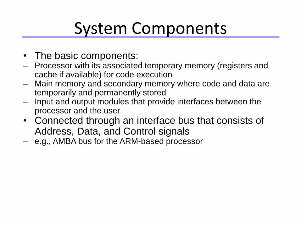
System Components
• The basic components:– Processor with its associated temporary memory (registers and
cache if available) for code execution– Main memory and secondary memory where code and data are
temporarily and permanently stored– Input and output modules that provide interfaces between the
processor and the user
• Connected through an interface bus that consists of Address, Data, and Control signals
– e.g., AMBA bus for the ARM-based processor

Universität Dortmund
Memory Hierarchy
• A typical processor is supported by:
– on-board main memory (e.g. SDRAM up to GB)
– on-chip or on-die cache memory (e.g. SRAM KB to MB)
– on-die registers
• Some processors also provide general purpose on-
chip
– SRAM (e.g. embedded processor) which may be configured as SRAM/Cache combination (e.g. TI’s DSP)
• Typically, a processor also utilizes secondary non-
volatile memory
– for permanent code and data storage like Flash-based memory and hard disks
Universität Dortmund
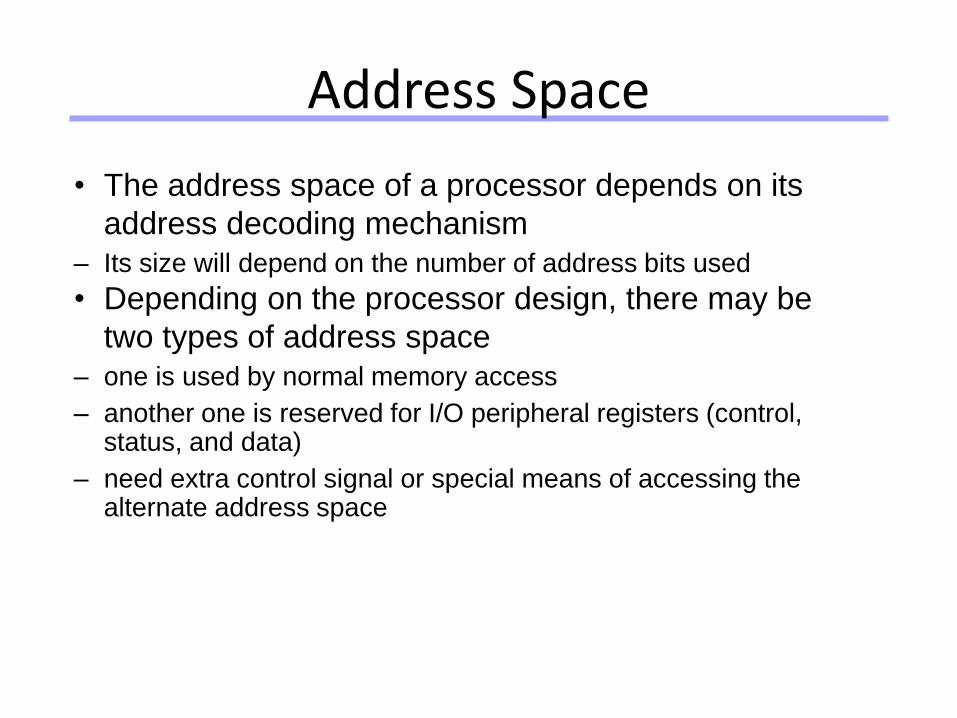
Address Space
• The address space of a processor depends on its
address decoding mechanism
– Its size will depend on the number of address bits used
• Depending on the processor design, there may be
two types of address space
– one is used by normal memory access
– another one is reserved for I/O peripheral registers (control, status, and data)
– need extra control signal or special means of accessing the alternate address space

Universität Dortmund
I/O Reg
I/O Reg
Memory
Processor
0x00000000
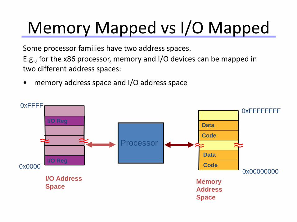
• Refer to the range of addresses that can be accessed
by the processor, determined by the number of
address bit utilized in the processor architecture
• Some processor families (e.g. ARM) utilize only one
address space for both memory and I/O devices
– i.e. everything is mapped in the same address space
0xFFFFFFFF
I/O
Data
Code
Address Space (con’t)
Universität Dortmund
Memory
Address
Space
Processor
0x00000000
Some processor families have two address spaces.
E.g., for the x86 processor, memory and I/O devices can be mapped in two different address spaces:
• memory address space and I/O address space
0xFFFFFFFF
0x0000
0xFFFF
I/O Address
Space
I/O Reg
I/O RegData
Code
Data
Code
Memory Mapped vs I/O Mapped
Universität Dortmund
• Two types of information are found in a typical program code:
i. Instruction codes for execution
ii. Data that is used by the instruction codes
• Two classes of memory systems designed to store the information:
i. von Neumann architecture
ii. Harvard architecture
Memory System Architectures

Universität Dortmund
0000h
FFFFh
Code
Data
Code
Data Table
Data
Processor
Single path
(bus) for both
Code & Data
• The von Neumann architecture utilizes only one memory bus for both instruction fetching and data access
– simplifies the hardware and glue logic design
– code and data located in the same address space
von Neumann Architecture
Universität Dortmund
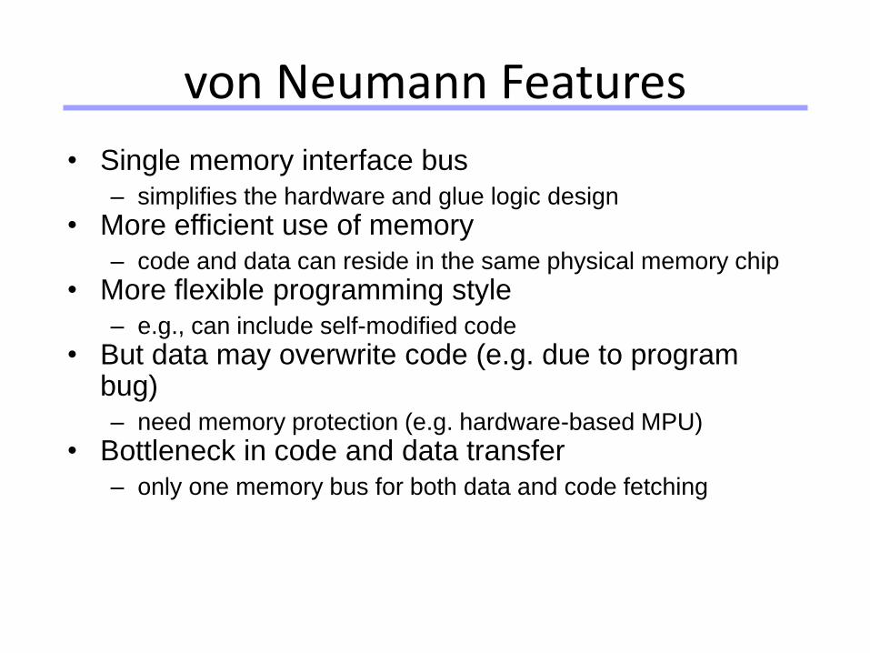
• Single memory interface bus
– simplifies the hardware and glue logic design
• More efficient use of memory
– code and data can reside in the same physical memory chip
• More flexible programming style
– e.g., can include self-modified code
• But data may overwrite code (e.g. due to program bug)
– need memory protection (e.g. hardware-based MPU)
• Bottleneck in code and data transfer
– only one memory bus for both data and code fetching
von Neumann Features

Universität Dortmund
• The Harvard architecture utilizes separate instruction bus and data bus
– code and data may still share the same memory space
0000h
FFFFh
Code
Code
Data
Data
ProcessorSeparate bus
for Code & Data
Data
Code7FFFh
8000h
Harvard Architecture

Universität Dortmund
• Separate instruction and data buses– allow code and data access at the same time which gives
improved performance
– provide better support for instruction pipeline operations and shorter instruction execution time
– allow different sizes of data and instructions to be used which results in more flexibility
– do not incur any code corruption by data which makes the operations more robust
• But more sophisticated hardware glue logic is required to support multiple interface buses
• Cortex-M4 core is based on the Harvard architecture with separate buses for instructions and data
Harvard Features

Universität Dortmund
0000h
FFFFh
Code
Code
Data
Data
Processor
Data
CodeFFFFh
0000h
0000h
FFFFh
Code
Data
Code
Data
Processor
Two separate
internal bus for
code & data (e.g.
ARM9)Data Cache
Code Cache
Independent data
and code memory
but with one shared
bus (e.g. 8051)
Architecture Variations

Universität Dortmund
00..00h
FF..FFh
Reset vector
Data
Program
Data
Processor
00..00h
FF..FFh
Program
Data
DataProcessor
Reset vector
Different processor families use different locations for their reset vectors for boot-up.
Examples:
• x86 processors boot up from the top of the memory space
• ARM processors boot up from the bottom of its memory space
Top Boot and Bottom Boot

Universität Dortmund
• Processor size is described in terms of ‘bits’ (e.g. an
8-bit or 32-bit processor)– corresponds to the data size that can be manipulated at a time by
the processor
– typically reflected in the size of the processor (internal) data path and register bank
• An 8-bit processor can only manipulate one byte of
data at a time, while a 32-bit processor can handle
one 32-bit double word sized data at a time– even though the data content may only be of single byte size
Processor ‘Size’

Universität Dortmund
• Typically, memory contains a storage locations that can store data of a certain fixed size– most commonly of the 8-bit (byte) size
• Each location is provided with a unique address.
• Depending on the data path size of the processor– the memory content is accessible in the size of an
8-bit byte, a 16-bit half word, a 32-bit word, and even a 64-bit double word
Data Organization in Memory

Universität Dortmund
• A 32-bit data consists of four bytes of data, which are stored in four successive memory locations
• Data and code must be aligned to the respective address size boundary. – e.g., for a 32-bit system which aligns to the word boundary, the
lowest two address bits equal to zero
• But what is the order of the four bytes of data?– depends on the Endianness adopted
• In the Little Endian format,
– the least significant byte (LSB) is stored in the lowest address of the memory, with the most significant byte (MSB) stored in the highest address location of the memory.
• In the Big Endian format,
– the least significant byte (LSB) is stored in the highest address of the memory, with the most significant byte (MSB) stored in the lowest address location of the memory.
Data Alignment

Universität Dortmund
Memory
Address
Space
0x000000
Memory
Address
Space
0x000000
MSB LSB
Big Endian Little Endian
Data Endianness
Universität Dortmund
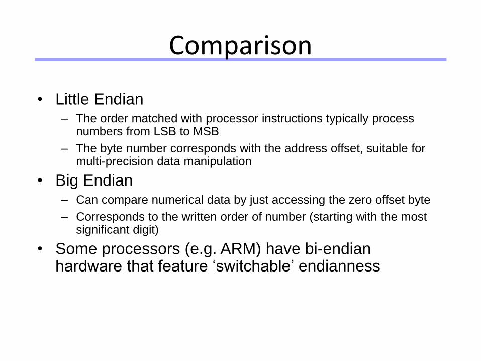
• Little Endian– The order matched with processor instructions typically process
numbers from LSB to MSB
– The byte number corresponds with the address offset, suitable for multi-precision data manipulation
• Big Endian– Can compare numerical data by just accessing the zero offset byte
– Corresponds to the written order of number (starting with the most significant digit)
• Some processors (e.g. ARM) have bi-endianhardware that feature ‘switchable’ endianness
Comparison

Universität Dortmund
Inside a Processor
Multi-ported register file
Processor datapath

Universität Dortmund
• The most fundamental storage area in the processor– is closely located to the processor
– provides very fast access, operating at the same frequency as the processor clock
– but is of limited quantity (typically less than 100)
• Most are of the general purpose type and can store
any type of information:
– data – e.g., timer value, constants
– address – e.g., ASCII table, stack
• Some are reserved for specific purposes– program counter (r15 in ARM)
– program status register (CPSR in ARM)
Registers

Universität Dortmund
Instructions
unused opcode regA regB unused destR
31-25 24-22 21-19 18-16 15-3 2-0
Instruction set architecture defines the mapping of assembly
instructions to machine code
add 1 2 3 // r3 = r1 + r2
Universität Dortmund
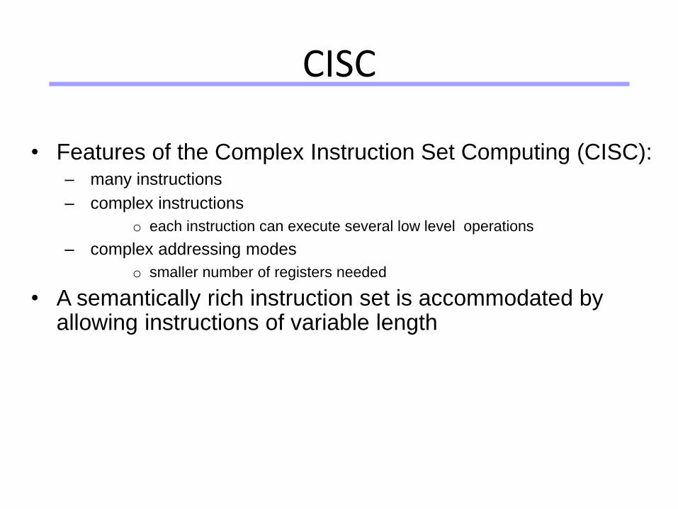
• Features of the Complex Instruction Set Computing (CISC):– many instructions
– complex instructions
o each instruction can execute several low level operations
– complex addressing modes
o smaller number of registers needed
• A semantically rich instruction set is accommodated by allowing instructions of variable length
CISC

Universität Dortmund
RISC – Reduced Instruction Set Computing
• Small instruction sets
• Simpler instructions
• Fixed length instructions
• Large number of registers
• Simpler addressing mode with the Load/Store instructions for accessing memory
RISC

Universität Dortmund
• Simpler instructions– one clock per instruction gives faster execution than on a CISC
processor with the same clock speed
• Simpler addressing mode– faster decoding
• Fixed length instructions– faster decoding and better pipeline performance
• Simpler hardware– less silicon area
– less power consumption
Advantages of RISC

Universität Dortmund
RISC Memory Footprint
• The RISC processor typically needs more memory than a CISC processor does to store the same program– complex functions performed in a single but slower instruction in
a CISC processor may require two, three, or more simpler instructions in a RISC processor
• To reduce memory requirements and cost – ARM provides the 16-bit Thumb instruction set as an option for its
RISC processor cores

Universität Dortmund
Limitations of RISC
• Fewer instructions than CISC– as compared to CISC, RISC needs more instructions to execute one
task
– code density is less
– needs more memory
• No complex instructions– no hardware support for division or floating-point arithmetic
operations
– needs a more complex compiler and longer compiling time
• But ARM also adds DSP-like instructions to support commonly used signal processing functions

Universität Dortmund
• Opcode encoding depends on the number of bits used– Example: For ARM, all instructions are of 32-bit length, but only 8
bits (bit 20 to 28) are used to encode the instruction. Hence a total of 28 = 256 different instructions are possible
• A typical instruction is encoded with a specific bit pattern that consists of the following:– an opcode field specifying the operation to be performed
– an operand(s) identification (address) field that depends on the modes of addressing;
o this provides the address of the register/memory location (s) that store the operand(s), or the operand itself.
Instruction Code Format
Universität Dortmund
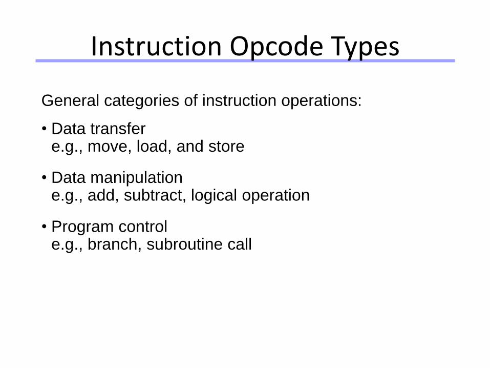
General categories of instruction operations:
• Data transfere.g., move, load, and store
• Data manipulatione.g., add, subtract, logical operation
• Program controle.g., branch, subroutine call
Instruction Opcode Types

Universität Dortmund
• Immediate addressing – operand is given in the instruction
• Register addressing– operand is stored in a register
• Direct addressing– operand is stored in memory, with the address given in the
instruction
• Indirect (Index) addressing– operand is stored in memory, with the address given in a register
(address and an offset given in the instruction)
• Implied addressing– implicit location like stack and program counter
Operand Addressing Types

Universität Dortmund
• Multiple stages are involved in executing an instruction.
– Example:
1) Fetching the instruction code
2) Decoding the instruction code
3) Executing the instruction code
• Hence multiple processor clock cycles are needed to execute one single instruction.
Fetch
Instruction
Decode
Instruction
Execute
Instruction
time
Fetch
Instruction
Decode
Instruction
Execute
Instruction
1st 2nd
Instruction Execution

Universität Dortmund
• The pipeline allows concurrent execution of multiple different instructions– execution of different stages of multiple instructions at the same time
• During a normal operation– while one instruction is being executed
– the next instruction is being decoded
– and a third instruction is being fetched from memory
– allows effective throughput to increase to one instruction per clock cycle
Instruction Pipeline

Universität Dortmund
Pipelined Execution
• 3-stage pipeline for instruction executions– Fetch Decode Execute
– Pipeline design allows effective throughput to increase to one instruction per clock cycle
– Allows the next instruction to be fetched while still decoding or executing the previous instructions
Fetch Decode Execute
Fetch Decode Execute
Fetch Decode Execute
1st
2nd
3rd
time

Universität Dortmund
Pipeline Hazards
• Not always one clock per cycle!
• Example: branch instruction “breaks” the pipe
Two stall cycles – don’t know if and where to jump
Universität Dortmund
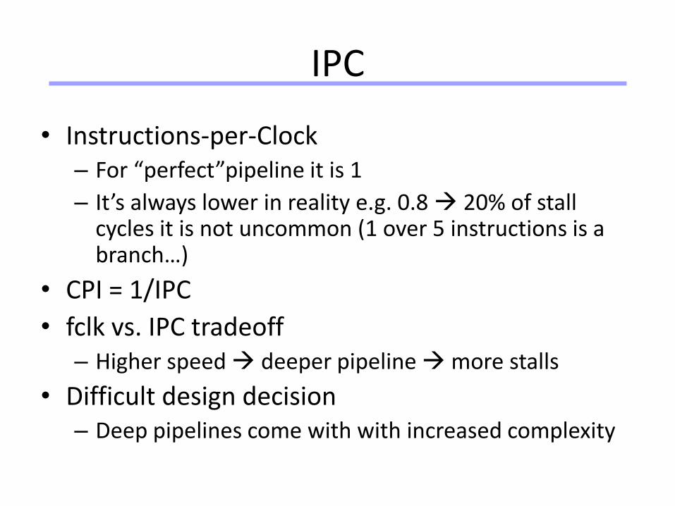
IPC
• Instructions-per-Clock– For “perfect”pipeline it is 1
– It’s always lower in reality e.g. 0.8 20% of stall cycles it is not uncommon (1 over 5 instructions is a branch…)
• CPI = 1/IPC
• fclk vs. IPC tradeoff– Higher speed deeper pipeline more stalls
• Difficult design decision– Deep pipelines come with with increased complexity

Universität Dortmund
ARM Processors Families
38

Universität Dortmund
• Key attributes: Implementation size, performance, and very low power.
• Architectures types:– ARMv4T architecture introduced the 16-bit Thumb® instruction
set alongside the 32-bit ARM instruction set.– ARMv5TEJ architecture introduced arithmetic support for digital
signal processing (DSP) algorithms.– ARMv6 architecture introduced an array of new features including
the Single Instruction Multiple Data (SIMD) operations.– ARMv7 architecture implementsThumb-2 technology.
• Cortex-A implements a virtual memory system architecture based on an MMU, an optional NEON processing unit for multimedia applications and advanced hardware Floating Point.
• Cortex-R – implements a protected memory system architecture based on an MPU (memory protection unit).
• Cortex-M – Microcontroller profile designed for fast interrupt processing.
– ARMv8 implementing 64bit instruction set
ARM Processors Architectures (2)
39Alberto Macii - Politecnico di Torino
Universität Dortmund
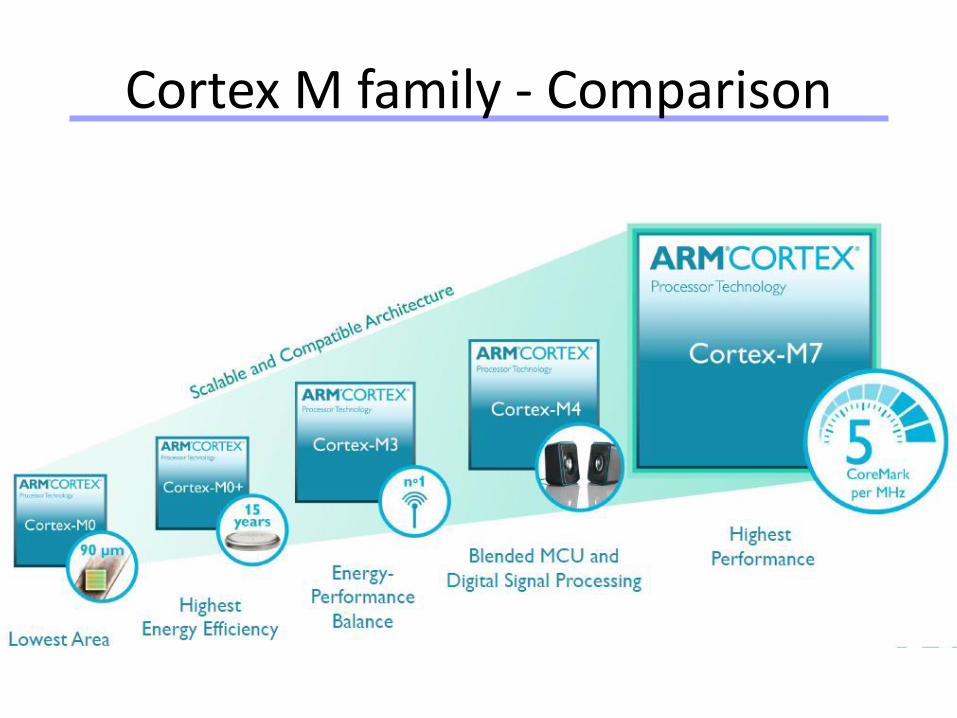
Cortex M family - Comparison

Universität Dortmund
Embedded ARM Cortex Processors
• Cortex M0:
– Ultra low gate count (less that 12 K gates).
– Ultra low-power (3 µW/MHz ).
– 32-bit processor.
41
Universität Dortmund
Embedded ARM Cortex Processors (2)
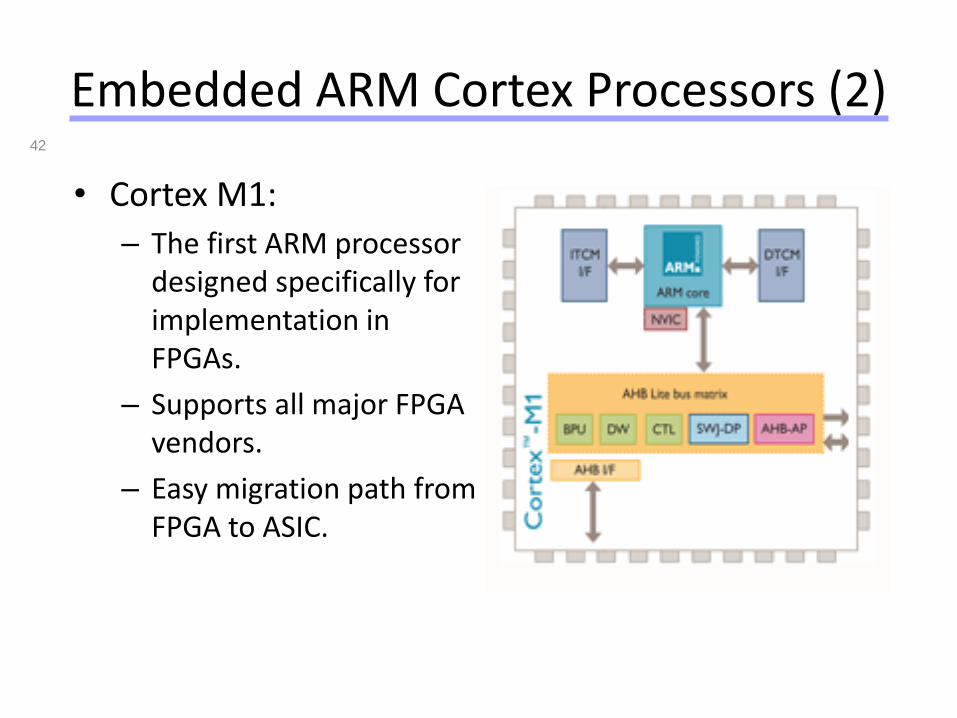
• Cortex M1:
– The first ARM processor designed specifically for implementation in FPGAs.
– Supports all major FPGA vendors.
– Easy migration path from FPGA to ASIC.
42

Universität Dortmund
Embedded ARM Cortex Processors
• Cortex M3:
– The mainstream ARM processor for microcontroller applications.
– High performance and energy efficiency.
43
Universität Dortmund
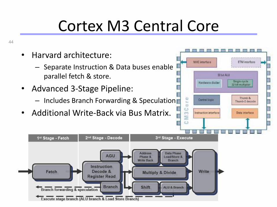
Cortex M3 Central Core
• Harvard architecture:– Separate Instruction & Data buses enable
parallel fetch & store.
• Advanced 3-Stage Pipeline:– Includes Branch Forwarding & Speculation
• Additional Write-Back via Bus Matrix.
44
Alberto Macii - Politecnico di Torino

Universität Dortmund
Embedded ARM Cortex Processors
45
Cortex M4
Embedded processor for DSP with FPU
Universität Dortmund
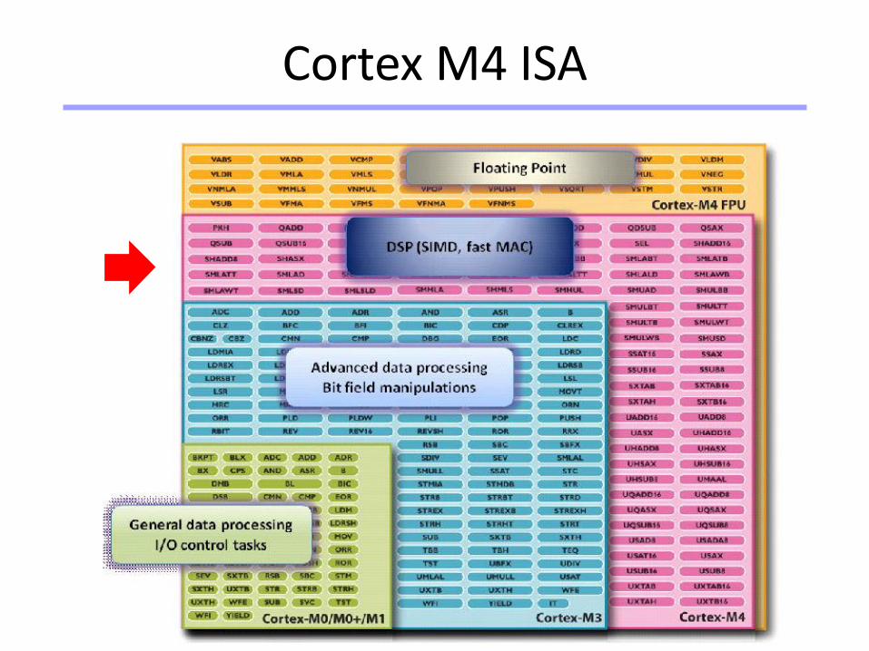
Cortex M4 ISA
Universität Dortmund
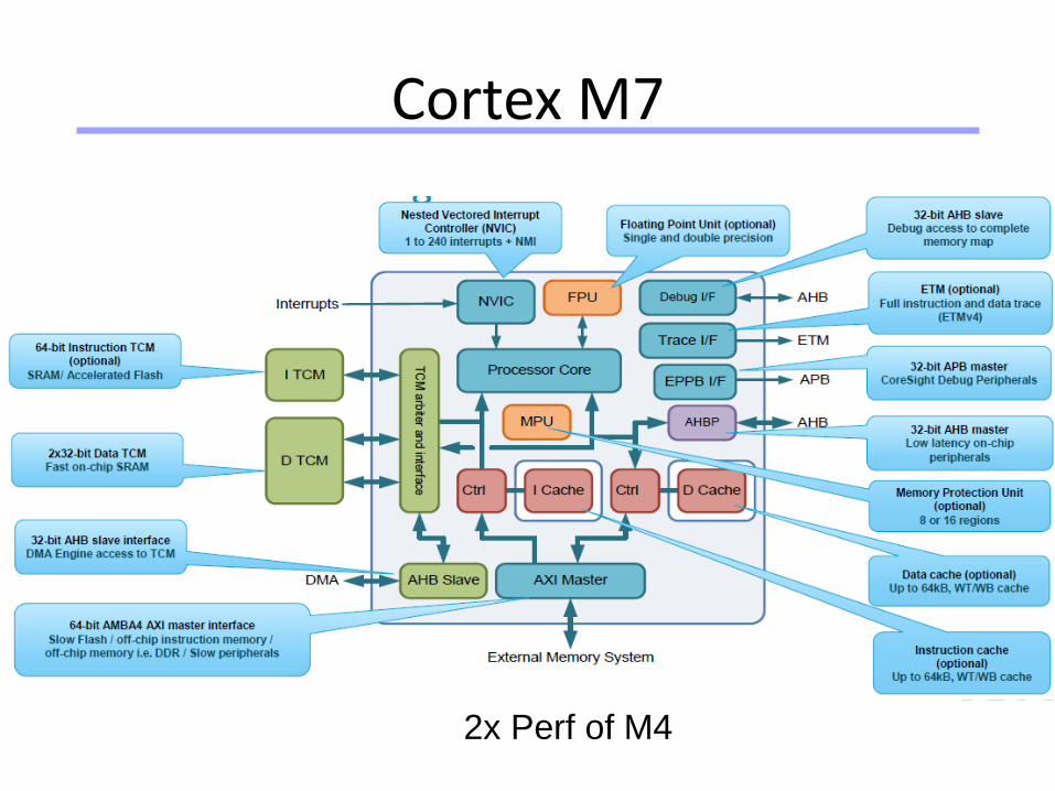
Cortex M7
2x Perf of M4

2
STM32F2x5
STM32F2x7
Ultra-low-power
Mainstream
Cortex-M0
Cortex-M0+Cortex-M3 Cortex-M4 Cortex-M7
STM32F030 Value line
STM32F0x1
STM32F0x2
STM32F0x8
STM32F301
STM32F302
STM32F303
STM32F3x4
STM32F373
STM32F3x8
STM32F100 Value line
STM32F101
STM32F102
STM32F103
STM32F105/107
STM32F401
STM32F411
STM32F405/415
STM32F407/417
STM32F427/437
STM32F429/439
STM32L0x1
STM32L0x2
STM32L0x3
STM32L100 Value line
STM32L151/152
STM32L162
High-performance
STM32 platform
STM32F746/756
8 product series / 30 product lines
STM32L47x
STM32L48x
STM32L43x
STM32L42x

Universität Dortmund
Application ARM Cortex Processors
• Cortex A15:
– Low-power.
– Suitable for:• Smartphones.
• Mobile Computing.
• Digital Home Entertainment.
• Wireless Infrastructure.
• Low-power Servers.
49
Universität Dortmund
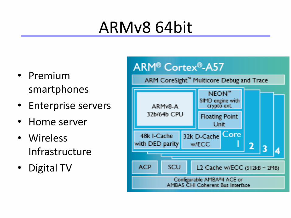
ARMv8 64bit
• Premium smartphones
• Enterprise servers
• Home server
• Wireless Infrastructure
• Digital TV

Universität Dortmund
Cortex A57 Block Diagram


