103
Arria 10 FPGA Development Kit User Guide Subscribe Send Feedback UG-01170 2015.06.26 101 Innovation Drive San Jose, CA 95134 www.altera.com

Arria 10 FPGA Development Kit UserGuide
Subscribe
Send Feedback
UG-011702015.06.26
101 Innovation DriveSan Jose, CA 95134www.altera.com

Contents
Overview.............................................................................................................. 1-1General Description.....................................................................................................................................1-1Recommended Operating Conditions...................................................................................................... 1-2Handling the Board..................................................................................................................................... 1-3
Getting Started.................................................................................................... 2-1Installing the Subscription Edition Software........................................................................................... 2-1
Activating Your License.................................................................................................................. 2-1Installing the Development Kit..................................................................................................................2-2Installing the USB-Blaster Driver.............................................................................................................. 2-3
Development Board Setup.................................................................................. 3-1Applying Power to the Board..................................................................................................................... 3-1Default Switch and Jumper Settings..........................................................................................................3-2
Board Test System............................................................................................... 4-1Preparing the Board.....................................................................................................................................4-2Running the Board Test System.................................................................................................................4-2Using the Board Test System......................................................................................................................4-4
Using the Configure Menu............................................................................................................. 4-4The System Info Tab........................................................................................................................4-5The GPIO Tab.................................................................................................................................. 4-7The Flash Tab................................................................................................................................... 4-9The XCVR Tab...............................................................................................................................4-11The PCIe Tab..................................................................................................................................4-14The FMC A Tab............................................................................................................................. 4-17The FMC B Tab..............................................................................................................................4-20The DDR3 Tab............................................................................................................................... 4-23The DDR4 Tab............................................................................................................................... 4-25The Power Monitor....................................................................................................................... 4-27The Clock Control......................................................................................................................... 4-29
Board Components..............................................................................................5-1Board Overview............................................................................................................................................5-1MAX V CPLD System Controller..............................................................................................................5-5FPGA Configuration................................................................................................................................. 5-15
Configuring the FPGA Using Programmer............................................................................... 5-15Status Elements.......................................................................................................................................... 5-15User Input/Output.....................................................................................................................................5-17
TOC-2 Arria 10 FPGA Development Kit
Altera Corporation
User-Defined Push Buttons..........................................................................................................5-17User-Defined DIP Switch............................................................................................................. 5-17User-Defined LEDs........................................................................................................................5-18Character LCD............................................................................................................................... 5-18DisplayPort..................................................................................................................................... 5-19SDI Video Input/Output Ports.................................................................................................... 5-20
Clock Circuitry...........................................................................................................................................5-23On-Board Oscillators.....................................................................................................................5-23Off-Board Clock I/O......................................................................................................................5-24
Components and Interfaces..................................................................................................................... 5-25PCI Express.....................................................................................................................................5-2510/100/1000 Ethernet PHY...........................................................................................................5-28HiLo External Memory Interface................................................................................................ 5-29FMC................................................................................................................................................. 5-36QSFP................................................................................................................................................ 5-43SFP+.................................................................................................................................................5-45I2C.................................................................................................................................................... 5-45
Memory....................................................................................................................................................... 5-48Flash................................................................................................................................................. 5-48
Board Power Supply.................................................................................................................................. 5-51Power Distribution System...........................................................................................................5-51Power Measurement......................................................................................................................5-52
Daughtercards............................................................................................................................................ 5-52External Memory Interface...........................................................................................................5-53FMC Loopback Card..................................................................................................................... 5-56
Additional Information......................................................................................A-1Board & User Guide Revision History.....................................................................................................A-1Compliance and Conformity Statements................................................................................................ A-1
CE EMI Conformity Caution........................................................................................................ A-1
Arria 10 FPGA Development Kit TOC-3
Altera Corporation

Overview 12015.06.26
UG-01170 Subscribe Send Feedback
The Arria® 10 GX FPGA development board provides a hardware platform for evaluating theperformance and features of the Altera® Arria 10 GX device.
General Description
Figure 1-1: Overview of the Development Board Features
FMCA (J1) FMCB (J2)Arria 10
FPGA (U28)Clock In/OutSMA (J6, J7) User Dipswitch
(SW2)Power Switch
(SW1)
PCIe ATXConnector(J4)
DC Input Jack (J13)
JTAG Header(J17)
Character LCD(B2)
Transceiver TX(J15, J16)
HiLo Connector(J14)
SDI Video Port(J20, J21)
PCI ExpressEdge Connector
(J22)
PCIe Dipswitch(SW3)
Fan Power Header (J19)
On-BoardUSB-Blaster II (J3)
DisplayPortConnector (J5)
MAX V CPLD (U16)
Gbps EthernetPort (J9)
QSPFInterface (J18)
LTPowerPlay interface Connector (J24)
© 2015 Altera Corporation. All rights reserved. ALTERA, ARRIA, CYCLONE, ENPIRION, MAX, MEGACORE, NIOS, QUARTUS and STRATIX words and logos aretrademarks of Altera Corporation and registered in the U.S. Patent and Trademark Office and in other countries. All other words and logos identified astrademarks or service marks are the property of their respective holders as described at www.altera.com/common/legal.html. Altera warrants performanceof its semiconductor products to current specifications in accordance with Altera's standard warranty, but reserves the right to make changes to anyproducts and services at any time without notice. Altera assumes no responsibility or liability arising out of the application or use of any information,product, or service described herein except as expressly agreed to in writing by Altera. Altera customers are advised to obtain the latest version of devicespecifications before relying on any published information and before placing orders for products or services.
ISO9001:2008Registered
www.altera.com101 Innovation Drive, San Jose, CA 95134

Figure 1-2: Arria 10 GX Block Diagram
FMCAltera LPC+
x69
CLKI
N x
8
REFC
LK x
2
XCVR
x16
XCVR
x8
x8 XCVRs
PCI Express 128MBFLASH x32
(FPGA)CPLDMAX V
x8 C
onfig
Oscillators50M, 125M,
Programmable
x1 (SE)
ButtonsSwitches
LEDs
x4x8
x16
x15
Micro-USB2.0
JTAG Chain
SMA CLK IN
NF5-1932C Package
10AX115N2F45
x32
x19 USB Interface
x4
HiLO External Memory
x136
x3 LCD
ENET FPGA (SGMII)
x8
EPCQ
On-BoardUSB Blaster TM II
& USB Interface
FMCAltera LPC+
x69
CLKI
N x
8
REFC
LK x
2
XCVR
x16
x66
x1(PCML)SMA XCVR OUT
x1SMA CLK OUT
QSFP x23
SFP+ x12
Display Port (TX)
x15
Arria 10 GXFPGA
MAX II
Related InformationBoard Components on page 5-1For details on the board components.
Recommended Operating Conditions• Recommended ambient operating temperature range: 0C to 45C• Maximum ICC load current: 80A• Maximum ICC load transient percentage: 35%• FPGA maximum power supported by the supplied heatsink/fan: 100W
1-2 Recommended Operating ConditionsUG-01170
2015.06.26
Altera Corporation Overview
Send Feedback

Handling the BoardWhen handling the board, it is important to observe static discharge precautions.
Caution: Without proper anti-static handling, the board can be damaged. Therefore, use anti-statichandling precautions when touching the board.
UG-011702015.06.26 Handling the Board 1-3
Overview Altera Corporation
Send Feedback
Getting Started 22015.06.26
UG-01170 Subscribe Send Feedback
Installing the Subscription Edition SoftwareThe Quartus II Subscription Edition Software provides the necessary tools used for developing hardwareand software for Altera devices.
Included in the Quartus II Subscription Edition Software are the Quartus II software, the Nios II EDS, andthe MegaCore IP Library. To install the Altera development tools, download the Quartus II SubscriptionEdition Software from the Quartus II Subscription Edition Software page of the Altera website. Alterna‐tively, you can request a DVD from the Altera IP and Software DVD Request Form page of the Alterawebsite.
Related InformationQuartus II Subscription Edition Software page
Activating Your LicensePurchasing this kit entitles you to a one-year license for the Development Kit Edition (DKE) of theQuartus II software. After the year, your DKE license will no longer be valid and you will not be permittedto use this version of the Quartus II software. To continue using the Quartus II software, you shoulddownload the free Quartus II Web Edition or purchase a subscription to Quartus II software.
Before using the Quartus II software, you must activate your license, identify specific users andcomputers, and obtain and install a license file. If you already have a licensed version of the subscriptionedition, you can use that license file with this kit. If not, follow these steps:
1. Log on at the myAltera Account Sign In web page, and click Sign In.2. On the myAltera Home web page, click the Self-Service Licensing Center link.3. Locate the serial number printed on the side of the development kit box below the bottom bar code.
The number consists of alphanumeric characters and does not contain hyphens.4. On the Self-Service Licensing Center web page, click the Find it with your License Activation Code
link.5. In the Find/Activate Products dialog box, enter your development kit serial number and click Search.
© 2015 Altera Corporation. All rights reserved. ALTERA, ARRIA, CYCLONE, ENPIRION, MAX, MEGACORE, NIOS, QUARTUS and STRATIX words and logos aretrademarks of Altera Corporation and registered in the U.S. Patent and Trademark Office and in other countries. All other words and logos identified astrademarks or service marks are the property of their respective holders as described at www.altera.com/common/legal.html. Altera warrants performanceof its semiconductor products to current specifications in accordance with Altera's standard warranty, but reserves the right to make changes to anyproducts and services at any time without notice. Altera assumes no responsibility or liability arising out of the application or use of any information,product, or service described herein except as expressly agreed to in writing by Altera. Altera customers are advised to obtain the latest version of devicespecifications before relying on any published information and before placing orders for products or services.
ISO9001:2008Registered
www.altera.com101 Innovation Drive, San Jose, CA 95134
6. When your product appears, turn on the check box next to the product name.7. Click Activate Selected Products, and click Close.8. When licensing is complete, Altera emails a license.dat file to you. Store the file on your computer and
use the License Setup page of the Options dialog box in the Quartus II software to enable the software.
Related Information
• Altera Software Installation and LicensingComprehensive information for installing and licensing Altera software.
• myAltera Account Sign In web page
Installing the Development Kit1. Download the Arria 10 FPGA Development Kit installer from the Arria 10 FPGA Development Kit
page of the Altera website. Alternatively, you can request a development kit DVD from the Altera KitInstallations DVD Request Form page of the Altera website.
2. Run the Arria 10 FPGA Development Kit installer.3. Follow the on-screen instructions to complete the installation process. Be sure that the installation
directory you choose is in the same relative location to the Quartus II software installation.The installation program creates the development kit directory structure shown in the following figure.
Figure 2-1: Installed Development Kit Directory Structure
<install dir>
documents
board_design_files
The default Windows installation directory is C:\altera\<version>\.
examples
factory_recovery
demos
kits
<device name>
Table 2-1: Installed Directory Contents
Directory Name Description of Contents
board_design_files Contains schematic, layout, assembly, and bill of material board design files.Use these files as a starting point for a new prototype board design.
demos Contains demonstration applications when available.
documents Contains the documentation.
examples Contains the sample design files for this kit.
2-2 Installing the Development KitUG-01170
2015.06.26
Altera Corporation Getting Started
Send Feedback

Directory Name Description of Contents
factory_recovery Contains the original data programmed onto the board before shipment. Usethis data to restore the board with its original factory contents.
Installing the USB-Blaster DriverThe development board includes integrated USB-Blaster circuitry for FPGA programming. However, forthe host computer and board to communicate, you must install the On-Board USB-Blaster II driver onthe host computer.
Installation instructions for the On-Board USB-Blaster II driver for your operating system are available onthe Altera website. On the Altera Programming Cable Driver Information page of the Altera website,locate the table entry for your configuration and click the link to access the instructions.
Related InformationAltera Programming Cable Driver InformationClick on the link for your operating system.
UG-011702015.06.26 Installing the USB-Blaster Driver 2-3
Getting Started Altera Corporation
Send Feedback
Development Board Setup 32015.06.26
UG-01170 Subscribe Send Feedback
This section describes how to apply power to the board and provides default switch and jumper settings.
Applying Power to the BoardThis development kit ships with its board switches preconfigured to support the design examples in thekit.
If you suspect that your board might not be currently configured with the default settings, follow theinstructions in the Default Switch and Jumper Settings section of this chapter.
1. The development board ships with design examples stored in the flash memory device. To load thedesign stored in the factory portion of flash memory, verify SW6.4 is set to OFF. This is the defaultsetting.
2. Connect the supplied power supply to an outlet and the DC Power Jack (J13) on the FPGA board.
Caution: Use only the supplied power supply. Power regulation circuitry on the board can bedamaged by power supplies with greater voltage.
3. Set the power switch (SW1) to the on position.
When the board powers up, the parallel flash loader (PFL) on the MAX V reads a design from flashmemory and configures the FPGA. When the configuration is complete, green LEDs illuminate signalingthe device configured successfully. If the configuration fails, the red LED illuminates.
© 2015 Altera Corporation. All rights reserved. ALTERA, ARRIA, CYCLONE, ENPIRION, MAX, MEGACORE, NIOS, QUARTUS and STRATIX words and logos aretrademarks of Altera Corporation and registered in the U.S. Patent and Trademark Office and in other countries. All other words and logos identified astrademarks or service marks are the property of their respective holders as described at www.altera.com/common/legal.html. Altera warrants performanceof its semiconductor products to current specifications in accordance with Altera's standard warranty, but reserves the right to make changes to anyproducts and services at any time without notice. Altera assumes no responsibility or liability arising out of the application or use of any information,product, or service described herein except as expressly agreed to in writing by Altera. Altera customers are advised to obtain the latest version of devicespecifications before relying on any published information and before placing orders for products or services.
ISO9001:2008Registered
www.altera.com101 Innovation Drive, San Jose, CA 95134

Default Switch and Jumper SettingsThis topic shows you how to restore the default factory settings and explains their functions.
Caution: Do not install or remove jumpers (shunts) while the development board is powered on.
Figure 3-1: Default Switch and Jumper Settings on the Top
FMCBFMCA
SW3
PRSNTn
ON12
34 X1
X4X8
FMCBVCCIO
1.8V1.5V1.35V
FMCA
J11 J8
Note for J11 & J 8:No shunt = 1.2V
1.35V1.5V1.8V
3-2 Default Switch and Jumper SettingsUG-01170
2015.06.26
Altera Corporation Development Board Setup
Send Feedback

Figure 3-2: Default Switch Settings on the Bottom
SW5
ON12
34
MSEL0MSEL1MSEL2VIDEN
SW4
CLK_SELCLK_ENSi516_FSFACTORYRZQ_B2K
ON1
1 0 1 0
23
4
ARRIA 10MAX VFMCAFMCB
SW6
ON12
34
5
1. Set DIP switch bank (SW3) to match the following table.
Table 3-1: SW3 DIP PCIe Switch Default Settings (Board Top)
Switch Board Label Function Default Position
1 x1 ON for PCIe x1 ON
2 x4 ON for PCIe x4 ON
3 x8 ON for PCIe x8 ON
4 — OFF for 1.35 V MEM_VDD power rail OFF
2. If all of the jumper blocks are open, the FMCA and FMCB VCCIO value is 1.2 V. To change that value,add shunts as shown in the following table.
Table 3-2: Default Jumper Settings for the FPGA Mezzanine Card (FMC) Ports (Board Top)
Board Reference Board Label Description
J8 pins 1-2 1.35V 1.35 V FMCB VCCIO select
J8 pins 3-4 1.5V 1.5 V FMCB VCCIO select
J8 pins 5-6 1.8V 1.8 V FMCB VCCIO select
J11 pins 1-2 1.35V 1.35 V FMCA VCCIO select
UG-011702015.06.26 Default Switch and Jumper Settings 3-3
Development Board Setup Altera Corporation
Send Feedback

Board Reference Board Label Description
J11 pins 3-4 1.5V 1.5 V FMCA VCCIO select
J11 pins 5-6 1.8V 1.8 V FMCA VCCIO select
3. Set DIP switch bank (SW4) to match the following table.
Table 3-3: SW4 JTAG DIP Switch Default Settings (Board Bottom)
Switch Board Label Function Default Position
1 ARRIA 10 OFF to enable the Arria 10 in the JTAG chain OFF
2 MAX V OFF to enable the MAX V in the JTAG chain OFF
3 FMCA ON to bypass the FMCA connector in the JTAGchain
ON
4 FMCB ON to bypass the FMCB connector in the JTAGchain
ON
4. Set DIP switch bank (SW5) to match the following table.
Table 3-4: SW5 DIP Switch Default Settings (Board Bottom)
Switch Board Label Function Default Position
1 MSEL0 ON for MSEL0 = 1; for FPP standard mode OFF
2 MSEL1 ON for MSEL1 = 0; for FPP standard mode ON
3 MSEL2 ON for MSEL2 = 0; for FPP standard mode ON
4 VIDEN OFF for enabling VID_EN for the Smart Voltage ID(SmartVID) feature
ON
5. Set DIP switch bank (SW6) to match the following table.
Table 3-5: SW6 DIP Switch Default Settings (Board Bottom)
Switch Board Label Function Default Position
1 CLK_SEL ON for 100 MHz on-board clock oscillatorselection
OFF for SMA input clock selection
ON
2 CLK_EN OFF for setting CLK_ENABLE signal high to theMAV V
OFF
3 Si516_FS ON for setting the SDI REFCLK frequency to148.35 MHz
OFF for setting the SDI REFCLK frequency to148.5 MHz
OFF
3-4 Default Switch and Jumper SettingsUG-01170
2015.06.26
Altera Corporation Development Board Setup
Send Feedback
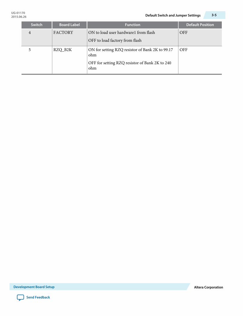
Switch Board Label Function Default Position
4 FACTORY ON to load user hardware1 from flash
OFF to load factory from flash
OFF
5 RZQ_B2K ON for setting RZQ resistor of Bank 2K to 99.17ohm
OFF for setting RZQ resistor of Bank 2K to 240ohm
OFF
UG-011702015.06.26 Default Switch and Jumper Settings 3-5
Development Board Setup Altera Corporation
Send Feedback
Board Test System 42015.06.26
UG-01170 Subscribe Send Feedback
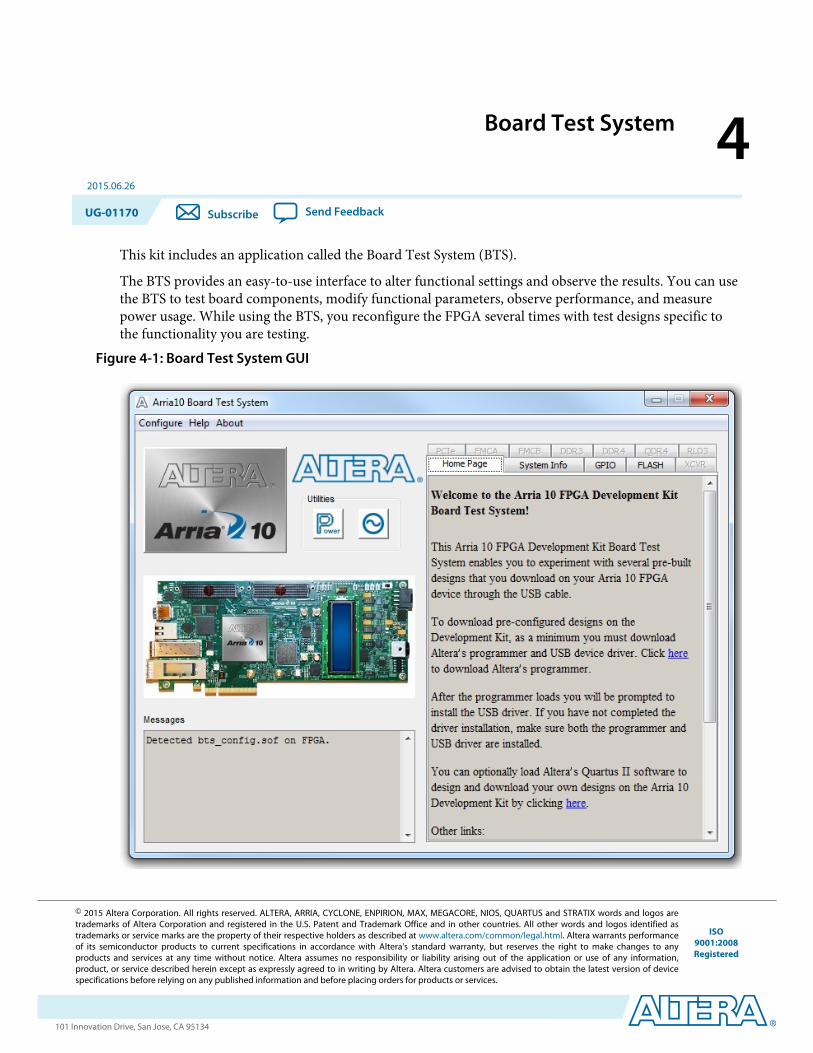
This kit includes an application called the Board Test System (BTS).
The BTS provides an easy-to-use interface to alter functional settings and observe the results. You can usethe BTS to test board components, modify functional parameters, observe performance, and measurepower usage. While using the BTS, you reconfigure the FPGA several times with test designs specific tothe functionality you are testing.
Figure 4-1: Board Test System GUI
© 2015 Altera Corporation. All rights reserved. ALTERA, ARRIA, CYCLONE, ENPIRION, MAX, MEGACORE, NIOS, QUARTUS and STRATIX words and logos aretrademarks of Altera Corporation and registered in the U.S. Patent and Trademark Office and in other countries. All other words and logos identified astrademarks or service marks are the property of their respective holders as described at www.altera.com/common/legal.html. Altera warrants performanceof its semiconductor products to current specifications in accordance with Altera's standard warranty, but reserves the right to make changes to anyproducts and services at any time without notice. Altera assumes no responsibility or liability arising out of the application or use of any information,product, or service described herein except as expressly agreed to in writing by Altera. Altera customers are advised to obtain the latest version of devicespecifications before relying on any published information and before placing orders for products or services.
ISO9001:2008Registered
www.altera.com101 Innovation Drive, San Jose, CA 95134

Several designs are provided to test the major board features. Each design provides data for one or moretabs in the application. The Configure menu identifies the appropriate design to download to the FPGAfor each tab.
After successful FPGA configuration, the appropriate tab appears that allows you to exercise the relatedboard features. Highlights appear in the board picture around the corresponding components
The BTS communicates over the JTAG bus to a test design running in the FPGA. The Board Test Systemand Power Monitor share the JTAG bus with other applications like the Nios II debugger and theSignalTap® II Embedded Logic Analyzer. Because the Quartus II programmer uses most of the bandwidthof the JTAG bus, other applications using the JTAG bus might time out. Be sure to close the other applica‐tions before attempting to reconfigure the FPGA using the Quartus II Programmer.
Preparing the BoardWith the power to the board off, follow these steps:
1. Connect the USB cable to your PC and the board.2. Ensure that the Ethernet patch cord is plugged into the RJ-45 connector.3. Check the development board switches and jumpers are set according to your preferences. See the
“Factory Default Switch and Jumper Settings” section.4. Set the load selector switch (SW6.4) to OFF for user hardware1 (page #1).
The development board ships with the CFI flash device preprogrammed with a default:
• Factory FPGA configuration for running the Board Update Portal design example• User configuration for running the Board Test System demonstration
5. Turn on the power to the board. The board loads the design stored in the user hardware1 portion offlash memory into the FPGA. If your board is still in the factory configuration, or if you havedownloaded a newer version of the Board Test System to flash memory through the Board UpdatePortal, the design loads the GPIO, Ethernet, and flash memory tests.To ensure operating stability, keep the USB cable connected and the board powered on when runningthe demonstration application. The application cannot run correctly unless the USB cable is attachedand the board is on.
Related InformationDefault Switch and Jumper Settings on page 3-2
Running the Board Test SystemTo run the Board Test System (BTS), navigate to the <install dir> \kits\<device name>\examples\board_test_system directory and run the BoardTestSystem(32-bit).exe or BoardTestSystem(64-bit).exe application.
On Windows, you can also run the BTS from the Start > All Programs > Altera menu.
A GUI appears, displaying the application tab that corresponds to the design running in the FPGA. Thedevelopment board’s flash memory ships preconfigured with the design that corresponds to the GPIO tab.
4-2 Preparing the BoardUG-01170
2015.06.26
Altera Corporation Board Test System
Send Feedback

Note: The BTS relies on the Quartus II software's specific library. Before running the BTS, open theQuartus II software. It sets the environment variable $QUARTUS_ROOTDIR automatically. The BoardTest System uses this environment variable to locate the Quartus II library.
UG-011702015.06.26 Running the Board Test System 4-3
Board Test System Altera Corporation
Send Feedback

Using the Board Test SystemThis section describes each control in the Board Test System application.
Using the Configure MenuUse the Configure menu to select the design you want to use. Each design example tests different boardfeatures. Choose a design from this menu and the corresponding tabs become active for testing.
Figure 4-2: The Configure Menu
To configure the FPGA with a test system design, perform the following steps:
1. On the Configure menu, click the configure command that corresponds to the functionality you wishto test.
2. In the dialog box that appears, click Configure to download the corresponding design to the FPGA.3. When configuration finishes, close the Quartus II Programmer if open. The design begins running in
the FPGA. The corresponding GUI application tabs that interface with the design are now enabled.
If you use the Quartus II Programmer for configuration, rather than the Board Test System GUI, you mayneed to restart the GUI.
4-4 Using the Board Test SystemUG-01170
2015.06.26
Altera Corporation Board Test System
Send Feedback
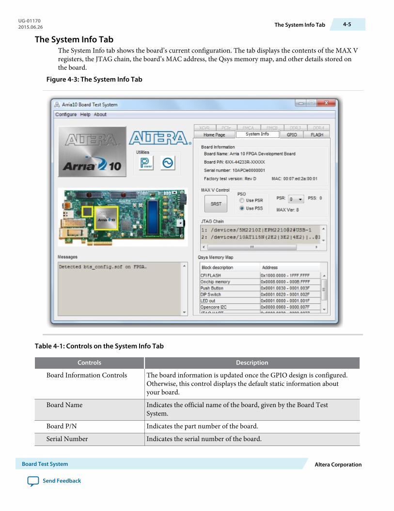
The System Info TabThe System Info tab shows the board’s current configuration. The tab displays the contents of the MAX Vregisters, the JTAG chain, the board’s MAC address, the Qsys memory map, and other details stored onthe board.
Figure 4-3: The System Info Tab
Table 4-1: Controls on the System Info Tab
Controls Description
Board Information Controls The board information is updated once the GPIO design is configured.Otherwise, this control displays the default static information aboutyour board.
Board Name Indicates the official name of the board, given by the Board TestSystem.
Board P/N Indicates the part number of the board.
Serial Number Indicates the serial number of the board.
UG-011702015.06.26 The System Info Tab 4-5
Board Test System Altera Corporation
Send Feedback

Controls Description
Factory Test Version Indicates the version of the Board Test System currently running onthe board.
MAC Indicates the MAC address of the board.
MAX V Control Allows you to view and change the current register values, which takeeffect immediately:
System Reset (SRST) — Write only. Click to reset the FPGA.
Page Select Override (PSO) — Read/Write
Page Select Register (PSR) — Read/Write
Page Select Switch (PSS) — Read only
MAX Ver: Indicates the version of MAX V code currently running onthe board.
JTAG Chain Shows all the devices currently in the JTAG chain.
Qsys Memory Map Shows the memory map of the Qsys system on your board.
4-6 The System Info TabUG-01170
2015.06.26
Altera Corporation Board Test System
Send Feedback
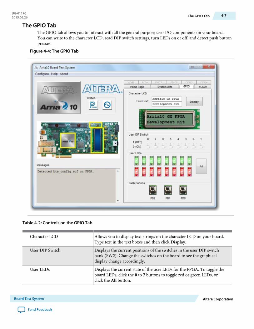
The GPIO TabThe GPIO tab allows you to interact with all the general purpose user I/O components on your board.You can write to the character LCD, read DIP switch settings, turn LEDs on or off, and detect push buttonpresses.
Figure 4-4: The GPIO Tab
Table 4-2: Controls on the GPIO Tab
Character LCD Allows you to display text strings on the character LCD on your board.Type text in the text boxes and then click Display.
User DIP Switch Displays the current positions of the switches in the user DIP switchbank (SW2). Change the switches on the board to see the graphicaldisplay change accordingly.
User LEDs Displays the current state of the user LEDs for the FPGA. To toggle theboard LEDs, click the 0 to 7 buttons to toggle red or green LEDs, orclick the All button.
UG-011702015.06.26 The GPIO Tab 4-7
Board Test System Altera Corporation
Send Feedback

Push Button Switches Read-only control displays the current state of the board user pushbuttons. Press a push button on the board to see the graphical displaychange accordingly.
4-8 The GPIO TabUG-01170
2015.06.26
Altera Corporation Board Test System
Send Feedback

The Flash TabThe Flash Tab allows you to read and write flash memory on your board. The memory table will displaythe CFI ROM table contents by default after you configure the FPGA.
Figure 4-5: The Flash Tab
Control Description
Read Reads the flash memory on your board. To see the flash memorycontents, type a starting address in the text box and click Read. Valuesstarting at the specified address appear in the table.
Write Writes the flash memory on your board. To update the flash memorycontents, change values in the table and click Write. The applicationwrites the new values to flash memory and then reads the values backto guarantee that the graphical display accurately reflects the memorycontents.
Random Test Starts a random data pattern test to flash memory, limited to the 512 Ktest system scratch page.
UG-011702015.06.26 The Flash Tab 4-9
Board Test System Altera Corporation
Send Feedback
Control Description
CFI Query Updates the memory table, displaying the CFI ROM table contentsfrom the flash device.
Increment Test Starts an incrementing data pattern test to flash memory, limited tothe 512 K test system scratch page.
Reset Executes the flash device’s reset command and updates the memorytable displayed on the Flash tab.
Erase Erases flash memory.Flash Memory Map Displays the flash memory map for the development board.
4-10 The Flash TabUG-01170
2015.06.26
Altera Corporation Board Test System
Send Feedback
The XCVR TabThis tab allows you to perform loopback tests on the QSFP, SFP, SMA, and SDI ports.
Figure 4-6: The XCVR Tab
UG-011702015.06.26 The XCVR Tab 4-11
Board Test System Altera Corporation
Send Feedback

Control Description
Status Displays the following status information during a loopback test:
PLL lock—Shows the PLL locked or unlocked state.
Pattern sync—Shows the pattern synced or not synced state. The pattern isconsidered synced when the start of the data sequence is detected.
Details—Shows the PLL lock and pattern sync status:
Port Allows you to specify which interface to test. The following port tests areavailable:
QSFP x4
SFP x1
SMA x1
SDI x1
PMA Setting Allows you to make changes to the PMA parameters that affect the activetransceiver interface. The following settings are available for analysis:
Serial Loopback—Routes signals between the transmitter and the receiver.
VOD—Specifies the voltage output differential of the transmitter buffer.
Pre-emphasis tap
• 1st pre—Specifies the amount of pre-emphasis on the pre-tap of thetransmitter buffer.
• 2nd pre—Specifies the amount of pre-emphasis on the second pre-tap ofthe transmitter buffer.
• 1st post—Specifies the amount of pre-emphasis on the first post tap of thetransmitter buffer.
• 2nd post—Specifies the amount of pre-emphasis on the second post tap ofthe transmitter buffer.
Equalizer—Specifies the setting for the receiver equalizer.
DC gain—Specifies the DC portion of the receiver equalizer.
4-12 The XCVR TabUG-01170
2015.06.26
Altera Corporation Board Test System
Send Feedback
Control Description
Data Type Specifies the type of data contained in the transactions. The following datatypes are available for analysis:
• PRBS 7—Selects pseudo-random 7-bit sequences.• PRBS 15—Selects pseudo-random 15-bit sequences.• PRBS 23—Selects pseudo-random 23-bit sequences.• PRBS 31—Selects pseudo-random 31-bit sequences.• HF—Selects highest frequency divide-by-2 data pattern 10101010.• LF—Selects lowest frequency divide by 33 data pattern.
Error Control Displays data errors detected during analysis and allows you to insert errors:
• Detected errors—Displays the number of data errors detected in thehardware.
• Inserted errors—Displays the number of errors inserted into the transmitdata stream.
• Insert Error—Inserts a one-word error into the transmit data stream eachtime you click the button. Insert Error is only enabled during transactionperformance analysis.
• Clear—Resets the Detected errors and Inserted errors counters to zeroes.
Loopback Start—Initiates the selected ports transaction performance analysis.
Note: Always click Clear before Start.
Stop—Terminates transaction performance analysis.
TX and RX performance bars—Show the percentage of maximum theoreticaldata rate that the requested transactions are able to achieve.
UG-011702015.06.26 The XCVR Tab 4-13
Board Test System Altera Corporation
Send Feedback

The PCIe TabThis tab allows you to run a PCIe loopback test on your board. You can also load the design and use anoscilloscope to measure an eye diagram of the PCIe transmit signals.
Figure 4-7: The PCIe Tab
4-14 The PCIe TabUG-01170
2015.06.26
Altera Corporation Board Test System
Send Feedback

Control Description
Status Displays the following status information during a loopback test:
PLL lock—Shows the PLL locked or unlocked state.
Pattern sync—Shows the pattern synced or not synced state. Thepattern is considered synced when the start of the data sequence isdetected.
Details—Shows the PLL lock and pattern sync status:
Port PCIe x8 Gen3PMA Setting Allows you to make changes to the PMA parameters that affect the
active transceiver interface. The following settings are available foranalysis:
Serial Loopback—Routes signals between the transmitter and thereceiver.
VOD—Specifies the voltage output differential of the transmitterbuffer.
Pre-emphasis tap
• 1st pre—Specifies the amount of pre-emphasis on the pre-tap of thetransmitter buffer.
• 2nd pre—Specifies the amount of pre-emphasis on the second pre-tap of the transmitter buffer.
• 1st post—Specifies the amount of pre-emphasis on the first post tapof the transmitter buffer.
• 2nd post—Specifies the amount of pre-emphasis on the secondpost tap of the transmitter buffer.
Equalizer—Specifies the setting for the receiver equalizer.
DC gain—Specifies the DC portion of the receiver equalizer.
UG-011702015.06.26 The PCIe Tab 4-15
Board Test System Altera Corporation
Send Feedback

Control Description
Data Type Specifies the type of data contained in the transactions. The followingdata types are available for analysis:
• PRBS 7—Selects pseudo-random 7-bit sequences.• PRBS 15—Selects pseudo-random 15-bit sequences.• PRBS 23—Selects pseudo-random 23-bit sequences.• PRBS 31—Selects pseudo-random 31-bit sequences.• HF—Selects highest frequency divide-by-2 data pattern 10101010.• LF—Selects lowest frequency divide by 33 data pattern.
Error Control Displays data errors detected during analysis and allows you to inserterrors:
• Detected errors—Displays the number of data errors detected inthe hardware.
• Inserted errors—Displays the number of errors inserted into thetransmit data stream.
• Insert Error—Inserts a one-word error into the transmit datastream each time you click the button. Insert Error is only enabledduring transaction performance analysis.
• Clear—Resets the Detected errors and Inserted errors counters tozeroes.
Loopback Start—Initiates the selected ports transaction performance analysis.
Note: Always click Clear before Start.
Stop—Terminates transaction performance analysis.
TX and RX performance bars—Show the percentage of maximumtheoretical data rate that the requested transactions are able to achieve.
4-16 The PCIe TabUG-01170
2015.06.26
Altera Corporation Board Test System
Send Feedback

The FMC A TabThis tab allows you to perform loopback tests on the FMC A port.
Figure 4-8: The FMC A Tab
UG-011702015.06.26 The FMC A Tab 4-17
Board Test System Altera Corporation
Send Feedback

Control Description
Status Displays the following status information during a loopback test:
PLL lock—Shows the PLL locked or unlocked state.
Pattern sync—Shows the pattern synced or not synced state. Thepattern is considered synced when the start of the data sequence isdetected.
Details—Shows the PLL lock and pattern sync status:
Port Allows you to specify which interface to test. The following port testsare available:
XCVR
CMOS
PMA Setting Allows you to make changes to the PMA parameters that affect theactive transceiver interface. The following settings are available foranalysis:
Serial Loopback—Routes signals between the transmitter and thereceiver.
VOD—Specifies the voltage output differential of the transmitterbuffer.
Pre-emphasis tap
• 1st pre—Specifies the amount of pre-emphasis on the pre-tap of thetransmitter buffer.
• 2nd pre—Specifies the amount of pre-emphasis on the second pre-tap of the transmitter buffer.
• 1st post—Specifies the amount of pre-emphasis on the first post tapof the transmitter buffer.
• 2nd post—Specifies the amount of pre-emphasis on the secondpost tap of the transmitter buffer.
Equalizer—Specifies the setting for the receiver equalizer.
DC gain—Specifies the DC portion of the receiver equalizer.
4-18 The FMC A TabUG-01170
2015.06.26
Altera Corporation Board Test System
Send Feedback
Control Description
Data Type Specifies the type of data contained in the transactions. The followingdata types are available for analysis:
• PRBS 7—Selects pseudo-random 7-bit sequences.• PRBS 15—Selects pseudo-random 15-bit sequences.• PRBS 23—Selects pseudo-random 23-bit sequences.• PRBS 31—Selects pseudo-random 31-bit sequences.• HF—Selects highest frequency divide-by-2 data pattern 10101010.• LF—Selects lowest frequency divide by 33 data pattern.
Error Control Displays data errors detected during analysis and allows you to inserterrors:
• Detected errors—Displays the number of data errors detected inthe hardware.
• Inserted errors—Displays the number of errors inserted into thetransmit data stream.
• Insert Error—Inserts a one-word error into the transmit datastream each time you click the button. Insert Error is only enabledduring transaction performance analysis.
• Clear—Resets the Detected errors and Inserted errors counters tozeroes.
Loopback Start—Initiates the selected ports transaction performance analysis.
Note: Always click Clear before Start.
Stop—Terminates transaction performance analysis.
TX and RX performance bars—Show the percentage of maximumtheoretical data rate that the requested transactions are able to achieve.
UG-011702015.06.26 The FMC A Tab 4-19
Board Test System Altera Corporation
Send Feedback
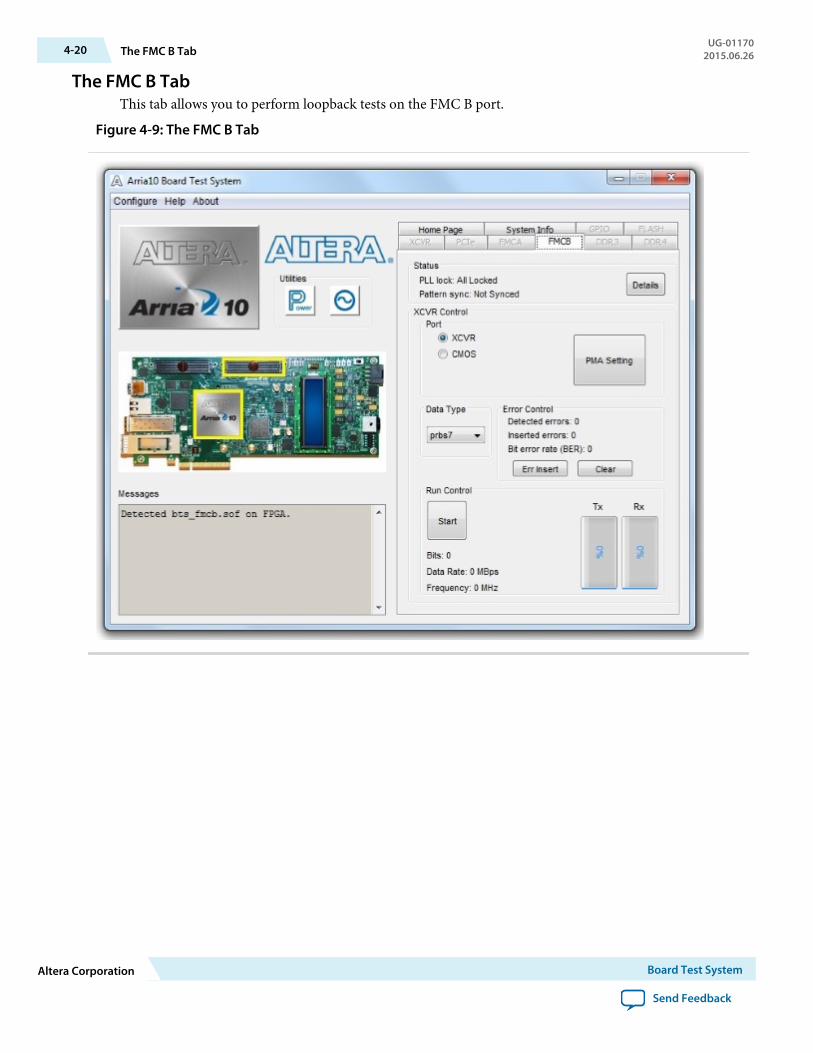
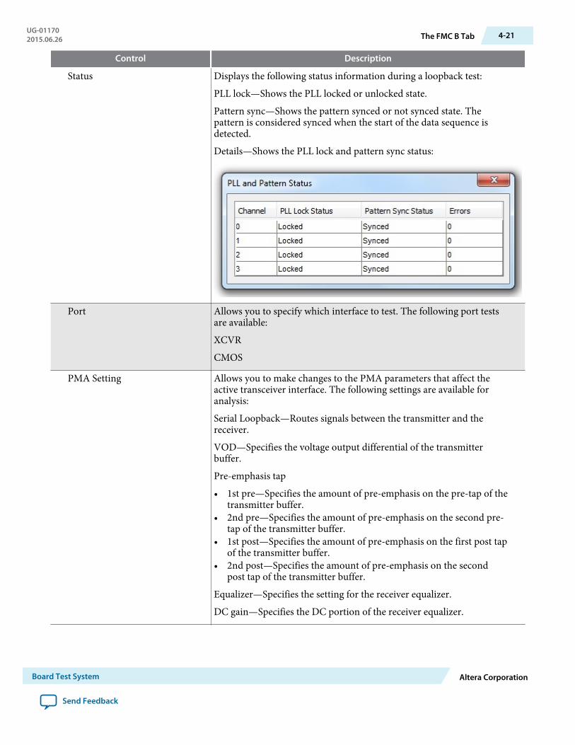
The FMC B TabThis tab allows you to perform loopback tests on the FMC B port.
Figure 4-9: The FMC B Tab
4-20 The FMC B TabUG-01170
2015.06.26
Altera Corporation Board Test System
Send Feedback
Control Description
Status Displays the following status information during a loopback test:
PLL lock—Shows the PLL locked or unlocked state.
Pattern sync—Shows the pattern synced or not synced state. Thepattern is considered synced when the start of the data sequence isdetected.
Details—Shows the PLL lock and pattern sync status:
Port Allows you to specify which interface to test. The following port testsare available:
XCVR
CMOS
PMA Setting Allows you to make changes to the PMA parameters that affect theactive transceiver interface. The following settings are available foranalysis:
Serial Loopback—Routes signals between the transmitter and thereceiver.
VOD—Specifies the voltage output differential of the transmitterbuffer.
Pre-emphasis tap
• 1st pre—Specifies the amount of pre-emphasis on the pre-tap of thetransmitter buffer.
• 2nd pre—Specifies the amount of pre-emphasis on the second pre-tap of the transmitter buffer.
• 1st post—Specifies the amount of pre-emphasis on the first post tapof the transmitter buffer.
• 2nd post—Specifies the amount of pre-emphasis on the secondpost tap of the transmitter buffer.
Equalizer—Specifies the setting for the receiver equalizer.
DC gain—Specifies the DC portion of the receiver equalizer.
UG-011702015.06.26 The FMC B Tab 4-21
Board Test System Altera Corporation
Send Feedback

Control Description
Data Type Specifies the type of data contained in the transactions. The followingdata types are available for analysis:
• PRBS 7—Selects pseudo-random 7-bit sequences.• PRBS 15—Selects pseudo-random 15-bit sequences.• PRBS 23—Selects pseudo-random 23-bit sequences.• PRBS 31—Selects pseudo-random 31-bit sequences.• HF—Selects highest frequency divide-by-2 data pattern 10101010.• LF—Selects lowest frequency divide by 33 data pattern.
Error Control Displays data errors detected during analysis and allows you to inserterrors:
• Detected errors—Displays the number of data errors detected inthe hardware.
• Inserted errors—Displays the number of errors inserted into thetransmit data stream.
• Insert Error—Inserts a one-word error into the transmit datastream each time you click the button. Insert Error is only enabledduring transaction performance analysis.
• Clear—Resets the Detected errors and Inserted errors counters tozeroes.
Loopback Start—Initiates the selected ports transaction performance analysis.
Note: Always click Clear before Start.
Stop—Terminates transaction performance analysis.
TX and RX performance bars—Show the percentage of maximumtheoretical data rate that the requested transactions are able to achieve.
4-22 The FMC B TabUG-01170
2015.06.26
Altera Corporation Board Test System
Send Feedback

The DDR3 TabThis tab allows you to read and write DDR3 memory on your board.
Figure 4-10: The DDR3 Tab
Control Description
Start Initiates DDR3 memory transaction performance analysis.Stop Terminates transaction performance analysis.
UG-011702015.06.26 The DDR3 Tab 4-23
Board Test System Altera Corporation
Send Feedback

Control Description
Performance Indicators These controls display current transaction performance analysisinformation collected since you last clicked Start:
• Write, Read, and Total performance bars—Show the percentage ofmaximum theoretical data rate that the requested transactions areable to achieve.
• Write (MBps), Read (MBps), and Total (MBps)—Show thenumber of bytes of data analyzed per second.
• Data bus: 72 bits (8 bits ECC) wide and the frequency is 1066 MHzdouble data rate. 2133 Megabits per second (Mbps) per pin.Equating to a theoretical maximum bandwidth of 136512 Mbps or17064 MBps.
Error Control This control displays data errors detected during analysis and allowsyou to insert errors:
• Detected errors—Displays the number of data errors detected inthe hardware.
• Inserted errors—Displays the number of errors inserted into thetransaction stream.
• Insert Error—Inserts a one-word error into the transaction streameach time you click the button. Insert Error is only enabled duringtransaction performance analysis.
• Clear—Resets the Detected errors and Inserted errors counters tozeroes.
Number of Addresses to Writeand Read
Determines the number of addresses to use in each iteration of readsand writes.
4-24 The DDR3 TabUG-01170
2015.06.26
Altera Corporation Board Test System
Send Feedback

The DDR4 TabThis tab allows you to read and write DDR4 memory on your board.
Figure 4-11: The DDR4 Tab
Control Description
Start Initiates DDR4 memory transaction performance analysis.Stop Terminates transaction performance analysis.
UG-011702015.06.26 The DDR4 Tab 4-25
Board Test System Altera Corporation
Send Feedback

Control Description
Performance Indicators These controls display current transaction performance analysisinformation collected since you last clicked Start:
• Write, Read, and Total performance bars—Show the percentage ofmaximum theoretical data rate that the requested transactions areable to achieve.
• Write (MBps), Read (MBps), and Total (MBps)—Show thenumber of bytes of data analyzed per second.
• Data bus: 72 bits (8 bits ECC) wide and the frequency is 1066 MHzdouble data rate. 2133 Megabits per second (Mbps) per pin.Equating to a theoretical maximum bandwidth of 136512 Mbps or17064 MBps.
Error Control This control displays data errors detected during analysis and allowsyou to insert errors:
• Detected errors—Displays the number of data errors detected inthe hardware.
• Inserted errors—Displays the number of errors inserted into thetransaction stream.
• Insert Error—Inserts a one-word error into the transaction streameach time you click the button. Insert Error is only enabled duringtransaction performance analysis.
• Clear—Resets the Detected errors and Inserted errors counters tozeroes.
Number of Addresses to Writeand Read
Determines the number of addresses to use in each iteration of readsand writes.
4-26 The DDR4 TabUG-01170
2015.06.26
Altera Corporation Board Test System
Send Feedback
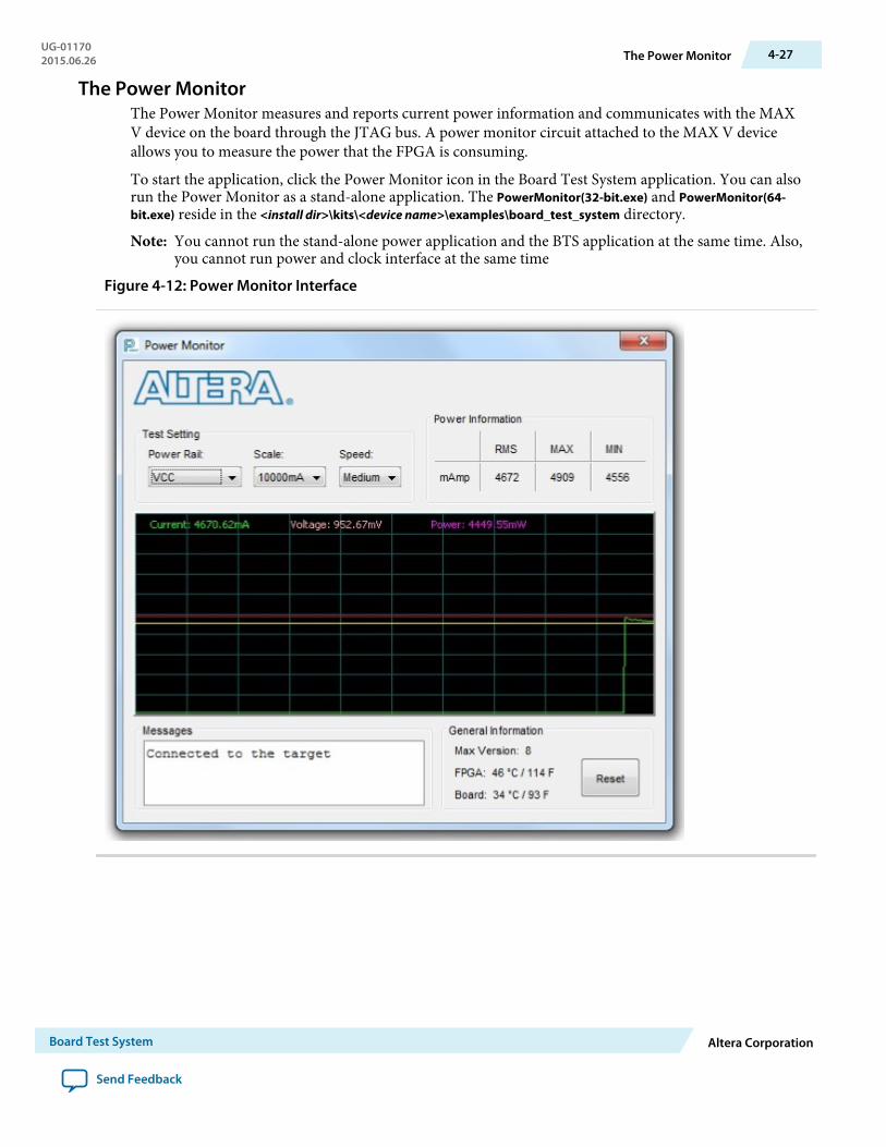
The Power MonitorThe Power Monitor measures and reports current power information and communicates with the MAXV device on the board through the JTAG bus. A power monitor circuit attached to the MAX V deviceallows you to measure the power that the FPGA is consuming.
To start the application, click the Power Monitor icon in the Board Test System application. You can alsorun the Power Monitor as a stand-alone application. The PowerMonitor(32-bit.exe) and PowerMonitor(64-bit.exe) reside in the <install dir>\kits\<device name>\examples\board_test_system directory.
Note: You cannot run the stand-alone power application and the BTS application at the same time. Also,you cannot run power and clock interface at the same time
Figure 4-12: Power Monitor Interface
UG-011702015.06.26 The Power Monitor 4-27
Board Test System Altera Corporation
Send Feedback

Control Description
Test Settings Displays the following controls:
Power Rail—Indicates the currently-selected power rail. Afterselecting the desired rail, click Reset to refresh the screen with updatedboard readings.
Scale—Specifies the amount to scale the power graph. Select a smallernumber to zoom in to see finer detail. Select a larger number to zoomout to see the entire range of recorded values.
Speed—Specifies how often to refresh the graph.
Power Information Displays root-mean-square (RMS) current, maximum, and minimumnumerical power readings in mA.
Graph Displays the mA power consumption of your board over time. Thegreen line indicates the current value. The red line indicates themaximum value read since the last reset. The yellow line indicates theminimum value read since the last reset.
General Information Displays MAX V version and current temperature of the FPGA andboard.
Reset Clears the graph, resets the minimum and maximum values, andrestarts the Power Monitor.
4-28 The Power MonitorUG-01170
2015.06.26
Altera Corporation Board Test System
Send Feedback
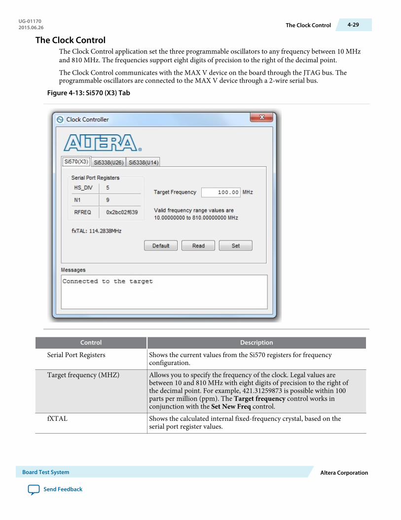
The Clock ControlThe Clock Control application set the three programmable oscillators to any frequency between 10 MHzand 810 MHz. The frequencies support eight digits of precision to the right of the decimal point.
The Clock Control communicates with the MAX V device on the board through the JTAG bus. Theprogrammable oscillators are connected to the MAX V device through a 2-wire serial bus.
Figure 4-13: Si570 (X3) Tab
Control Description
Serial Port Registers Shows the current values from the Si570 registers for frequencyconfiguration.
Target frequency (MHZ) Allows you to specify the frequency of the clock. Legal values arebetween 10 and 810 MHz with eight digits of precision to the right ofthe decimal point. For example, 421.31259873 is possible within 100parts per million (ppm). The Target frequency control works inconjunction with the Set New Freq control.
fXTAL Shows the calculated internal fixed-frequency crystal, based on theserial port register values.
UG-011702015.06.26 The Clock Control 4-29
Board Test System Altera Corporation
Send Feedback
Control Description
Default Sets the frequency for the oscillator associated with the active tab backto its default value. This can also be accomplished by power cycling theboard.
Set New Freq Sets the programmable oscillator frequency for the selected clock tothe value in the Target frequency control for the programmableoscillators. Frequency changes might take several milliseconds to takeeffect. You might see glitches on the clock during this time. Alterarecommends resetting the FPGA logic after changing frequencies.
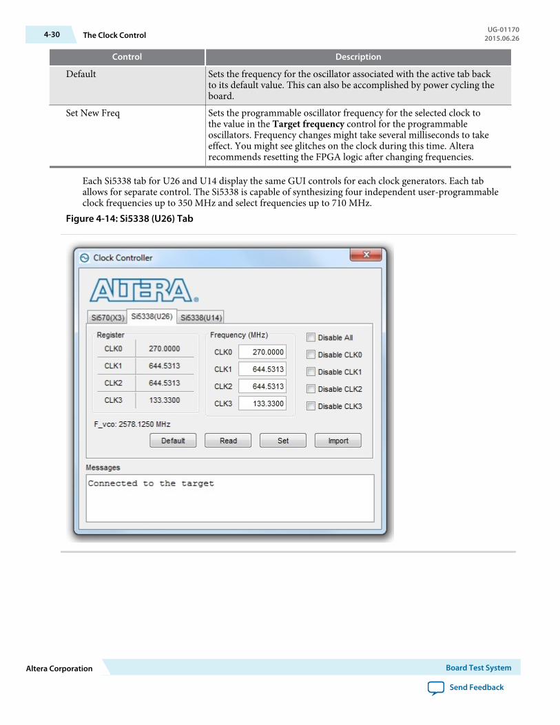
Each Si5338 tab for U26 and U14 display the same GUI controls for each clock generators. Each taballows for separate control. The Si5338 is capable of synthesizing four independent user-programmableclock frequencies up to 350 MHz and select frequencies up to 710 MHz.
Figure 4-14: Si5338 (U26) Tab
4-30 The Clock ControlUG-01170
2015.06.26
Altera Corporation Board Test System
Send Feedback

Figure 4-15: Si5338 (U14) Tab
Control Description
F_vco Displays the generating signal value of the voltage-controlledoscillator.
Registers Display the current frequencies for each oscillator.Frequency (MHz) Allows you to specify the frequency of the clock.Disable all Disable all oscillators at once.Read Reads the current frequency setting for the oscillator associated with
the active tab.Default Sets the frequency for the oscillator associated with the active tab back
to its default value. This can also be accomplished by power cycling theboard.
Set New Freq Sets the programmable oscillator frequency for the selected clock tothe value in the CLK0 to CLK3 controls for the Si5338 (U26 and U14).Frequency changes might take several milliseconds to take effect. Youmight see glitches on the clock during this time. Altera recommendsresetting the FPGA logic after changing frequencies.
UG-011702015.06.26 The Clock Control 4-31
Board Test System Altera Corporation
Send Feedback
Control Description
Import Reg Map Import register map file generated from Silicon LaboratoriesClockBuilder Desktop.
4-32 The Clock ControlUG-01170
2015.06.26
Altera Corporation Board Test System
Send Feedback

Board Components 52015.06.26
UG-01170 Subscribe Send Feedback
This chapter introduces all the important components on the development kit board.
A complete set of schematics, a physical layout database, and GERBER files for the development boardreside in the development kit documents directory.
Board OverviewThis section provides an annotated board image and the major component descriptions.
Figure 5-1: Overview of the Development Board Features
FMCA (J1) FMCB (J2)Arria 10
FPGA (U28)Clock In/OutSMA (J6, J7) User Dipswitch
(SW2)Power Switch
(SW1)
PCIe ATXConnector(J4)
DC Input Jack (J13)
JTAG Header(J17)
Character LCD(B2)
Transceiver TX(J15, J16)
HiLo Connector(J14)
SDI Video Port(J20, J21)
PCI ExpressEdge Connector
(J22)
PCIe Dipswitch(SW3)
Fan Power Header (J19)
On-BoardUSB-Blaster II (J3)
DisplayPortConnector (J5)
MAX V CPLD (U16)
Gbps EthernetPort (J9)
QSPFInterface (J18)
LTPowerPlay interface Connector (J24)
© 2015 Altera Corporation. All rights reserved. ALTERA, ARRIA, CYCLONE, ENPIRION, MAX, MEGACORE, NIOS, QUARTUS and STRATIX words and logos aretrademarks of Altera Corporation and registered in the U.S. Patent and Trademark Office and in other countries. All other words and logos identified astrademarks or service marks are the property of their respective holders as described at www.altera.com/common/legal.html. Altera warrants performanceof its semiconductor products to current specifications in accordance with Altera's standard warranty, but reserves the right to make changes to anyproducts and services at any time without notice. Altera assumes no responsibility or liability arising out of the application or use of any information,product, or service described herein except as expressly agreed to in writing by Altera. Altera customers are advised to obtain the latest version of devicespecifications before relying on any published information and before placing orders for products or services.
ISO9001:2008Registered
www.altera.com101 Innovation Drive, San Jose, CA 95134

Table 5-1: Arria 10 GX FPGA Development Board Components
Board Reference Type Description
Featured Devices
U28 FPGA Arria 10 GX FPGA, 10AX115S2F45I1SG:
• Adaptive logic modules (ALMs): 427,200• LEs (K): 1,150• Registers: 1,708,800• M20K memory blocks: 2,713• Transceiver count: 96• Package Type: 1932 BGA
U16 CPLD MAX V CPLD, 2210 LEs, 256FBGA 1.8V VCCINT
Board Reference Type Description
Configuration and Setup Elements
J3 On-Board USB-Blaster II Micro-USB 2.0 connector for programming anddebugging the FPGA.
SW3 PCI Express Control DIPswitch
Enables PCI Express link widths x1, x4, and x8.
SW4 JTAG Bypass DIP switch Enables and disables devices in the JTAG chain. Thisswitch is located on the back of the board.
SW5 FPP Configuration DIPSwitch
Sets the Arria 10 MSEL pins and VID_EN pin.
SW6 Board settings DIP switch Controls the MAX V CPLD System Controllerfunctions such as clock select, clock enable, factory oruser design load from flash and FACTORY signalcommand sent at power up. This switch is located atthe bottom of the board.
S4 CPU reset push button The default reset for the FPGA logic.S5 Image select push button Toggles the configuration LEDs which selects the
program image that loads from flash memory to theFPGA.
S6 Program configuration pushbutton
Configures the FPGA from flash memory image basedon the program LEDs.
S7 MAX V reset push button The default reset for the MAX V CPLD SystemController.
Board Reference Type Description
Status Elements
D22, D23 JTAG LEDs Indicates transmit or receive activity of the JTAGchain. The TX and RX LEDs flicker if the link is in useand active.
5-2 Board OverviewUG-01170
2015.06.26
Altera Corporation Board Components
Send Feedback

Board Reference Type Description
Status Elements
D24, D25 System Console LEDs Indicates the transmit or receive activity of the SystemConsole USB interface. The TX and RX LEDs wouldflicker if the link is in use and active. The LEDs areeither off when not in use or on when in use but idle.
D12, D13, D14 Program LEDs Illuminates to show the LED sequence that determineswhich flash memory image loads to the FPGA whenyou press the program load push button.
D17 Configuration done LED Illuminates when the FPGA is configured.D15 Load LED Illuminates during FPGA configuration.D16 Error LED Illuminates when the FPGA configuration from flash
fails.D19 Power LED Illuminates when the board is powered on.D32 Temperature LED Illuminates when an over temperature condition
occurs for the FPGA device. Ensure that an adequateheatsink/fan is properly installed..
D26, D27, D28,D29, D30
Ethernet LEDs Shows the connection speed as well as transmit orreceive activity.
D33 SDI Cable LED Illuminates to show the transmit or receive activity.D34, D35, D36,D37, D38
PCI Express link LEDs You can configure these LEDs to display the PCIExpress link width (x1, x4, x8) and data rate.
D3, D4, D5, D6,D7, D8, D9, D10
User defined LEDs Eight bi-color LEDs (green and red) for 16 user LEDs.Illuminates when driven low.
D1, D2, D11 FMCA LEDs Illuminates for RX, TX, PRSNTn activity.D18, D20, D21 FMCB LEDs Illuminates for RX, TX, PRSNTn activity.
Board Reference Type Description
Clock Circuitry
X1 SDI reference clock SW6.3 DIP switch controlled:
FS=0: 148.35 MHz
FS=1: 148.50 MHz
X3 Programmable oscillator Si570 programmable oscillator by the clock controlGUI. Default is 100 MHz.
X2 125.0-MHz oscillator 125.0-MHz voltage controlled crystal oscillator for theEthernet interface..
X4 50-MHz oscillator 50.000-MHz crystal oscillator for general purpose logic.U26 Quad-output oscillator Si5338 programmable oscillator for clock control GUI.
(Defaults CLK[0:3] = 270MHz, 644.53125MHz,644.53125MHz, 133.33MHz)
UG-011702015.06.26 Board Overview 5-3
Board Components Altera Corporation
Send Feedback

Board Reference Type Description
Clock Circuitry
U14 Quad-output oscillator Si5338 programmable oscillator for clock control GUI.(Defaults CLK[0:3] = 100MHz, 625MHz, 625MHz,302.083333MHz)
J6 Clock input SMA connector Signal: CLKIN_SMAJ7 Clock output SMA connector Signal: SMA_CLK_OUTJ20, J21 SDI (Serial Digital Interface)
transceiver connectorsTwo sub-miniature version B (SMB) connectors.Drives serial data input/output to or from SDI videoport.
Board Reference Type Description
Transceiver Interfaces
J15 SMA connector SMA_TX_N from the left transceiver bank - 1HJ16 SMA connector SMA_TX_P from the left transceiver bank - 1H
Board Reference Type Description
General User Input/Output
SW2 FPGA user DIP switch Octal user DIP switches. When the switch is ON, alogic 0 is selected.
S1, S2, S3 General user push buttons Three user push buttons. Driven low when pressed.D3, D4, D5, D6,D7, D8, D9, D10
User defined LEDs Eight bi-color user LEDs. Illuminates when driven low.
Board Reference Type Description
Memory Devices
J14 HiLo Connector One x72 memory interface supporting DDR3 (x72),DDR4 (x72), QDR4 (x36), and RLDRAM 3 (x36).
This development kit includes three plugin modules(daughtercards) that use the HiLo connector:
• DDR4 memory (x72) 1333 MHz, Ping Pong PHY.• DDR3 memory (x72) 1066 MHz, Ping Pong PHY.• RLDRAM3 memory (x36) 1,200 MHz
U4, U5 Flash memory ICS - 1GBIT STRATA FLASH, 16-BIT DATA,VCC=VCCQ=1.7V-2.0V, 64-BALL EASY BGA(10MM X 8MM)
Board Reference Type Description
Communication Ports
J22 PCI Express x8 edgeconnector
Made of gold-plated edge fingers for up to ×8 signalingin either Gen1, Gen2, or Gen3 mode.
J1, J2 FMC Port FPGA mezzanine card ports A and B.
5-4 Board OverviewUG-01170
2015.06.26
Altera Corporation Board Components
Send Feedback

Board Reference Type Description
Communication Ports
J9 Gbps Ethernet RJ-45connector
RJ-45 connector which provides a 10/100/1000Ethernet connection via a Marvell 88E1111 PHY andthe FPGA-based Altera Triple Speed Ethernet MACMegaCore function in SGMII mode.
J18 QSFP interface Provides four transceiver channels for a 40G QSFPmodule.
J12 SFP+ connector SFP+ XCVR interface.J3 Micro-USB connector Embedded Altera USB-Blaster II JTAG for program‐
ming the FPGA via a USB cable.
Board Reference Type Description
Display Ports
J5 DisplayPort connector Molex 0.50mm pitch DisplayPort male receptacle, rightangle, surface mount, 0.76µm gold plating, 20 circuitswith cover.
B2 Character LCD Connector which interfaces to the provided 16character × 2 line LCD module.
J20, J21 SDI video port Two sub-miniature version B (SMB) connectors thatprovide a full-duplex SDI interface.
Board Reference Type Description
Power Supply
J22 PCI Express edge connector Interfaces to a PCI Express root port such as anappropriate PC motherboard.
J13 DC input jack Accepts a 12-V DC power supply. Do not use thisinput jack while the board is plugged into a PCIExpress slot.
SW1 Power Switch Switch to power on or off the board when power issupplied from the DC input jack.
J4 PCIe 2x4 ATX powerconnector
12-V ATX input. This input must be connected whenthe board is plugged into a PCIe root port.
MAX V CPLD System ControllerThe board utilizes the EPM2210 System Controller, an Altera MAX V CPLD, for the following purposes:
• FPGA configuration from flash memory• Power consumption monitoring• Temperature monitoring• Fan control• Control registers for clocks• Control registers for remote update system
UG-011702015.06.26 MAX V CPLD System Controller 5-5
Board Components Altera Corporation
Send Feedback

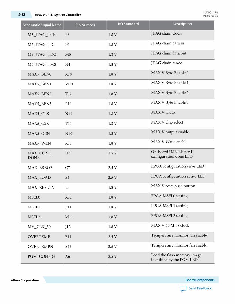
Table 5-2: MAX V CPLD System Controller Device Pin-Out
Schematic Signal Name Pin Number I/O Standard Description
CLK125_EN E9 2.5 V 125 MHz oscillator enable
CLK50_EN J16 1.8 V 50 MHz oscillator enable
CLK_CONFIG J5 1.8 V Clock Configure
CLK_ENABLE D4 2.5 V Clock Enable
CLK_SEL A2 2.5 V Clock Select
CLOCK_I2C_SCL C12 2.5 V Serial clock line for I2C
CLOCK_I2C_SDA C10 2.5 V Serial data line for I2C
CPU_RESETN K4 1.8 V FPGA reset push button
FACTORY_LOAD B5 2.5 V DIP switch to load factory oruser design at power-up
FLASH_ADVN N14 1.8 V FSM bus flash memory addressvalid
FLASH_CEN0 D14 1.8 V FSM bus flash memory chipenable
FLASH_CEN1 F11 1.8 V FSM bus flash memory chipenable
FLASH_CLK N15 1.8 V FSM bus flash memory clock
FLASH_OEN P14 1.8 V FSM bus flash memory outputenable
FLASH_RDYBSYN0
F12 1.8 V FSM bus flash memory ready
FLASH_RDYBSYN1
P15 1.8 V FSM bus flash memory ready
FLASH_RESETN D13 1.8 V FSM bus flash memory reset
FLASH_WEN J1 1.8 V FSM bus flash memory writeenable
FM_A1 F15 1.8 V FM address bus
FM_A2 G16 1.8 V FM address bus
FM_A3 G15 1.8 V FM address bus
5-6 MAX V CPLD System ControllerUG-01170
2015.06.26
Altera Corporation Board Components
Send Feedback
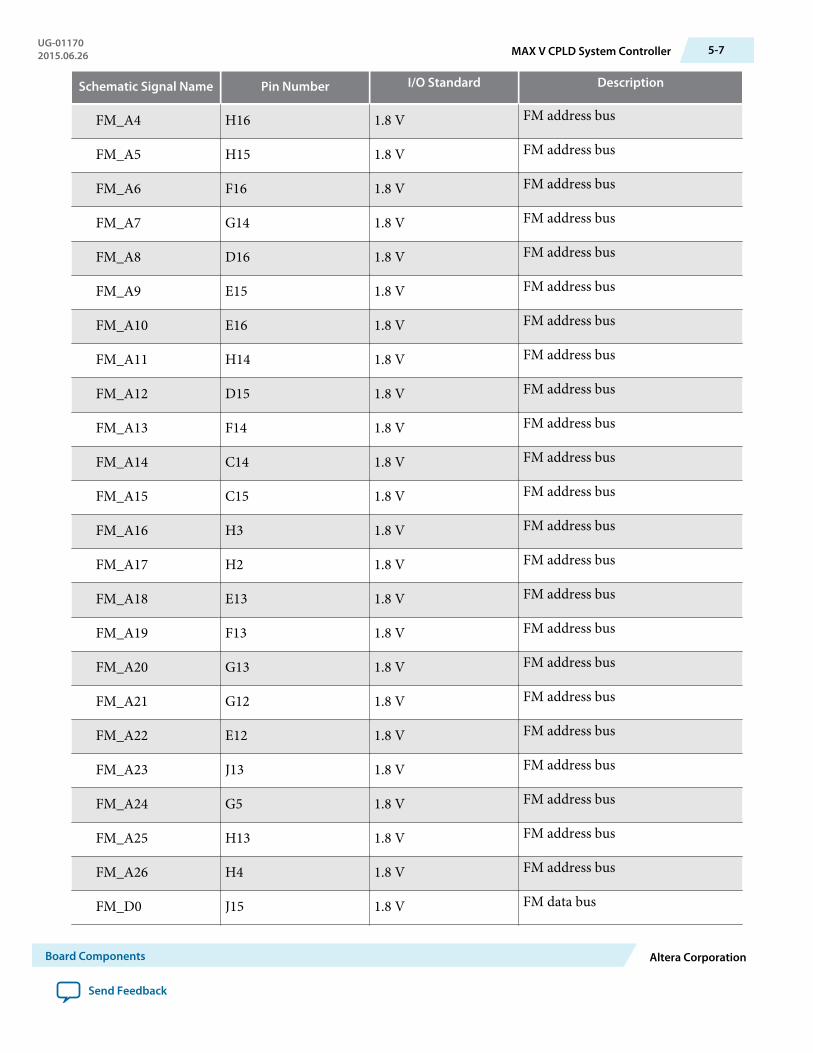
Schematic Signal Name Pin Number I/O Standard Description
FM_A4 H16 1.8 V FM address bus
FM_A5 H15 1.8 V FM address bus
FM_A6 F16 1.8 V FM address bus
FM_A7 G14 1.8 V FM address bus
FM_A8 D16 1.8 V FM address bus
FM_A9 E15 1.8 V FM address bus
FM_A10 E16 1.8 V FM address bus
FM_A11 H14 1.8 V FM address bus
FM_A12 D15 1.8 V FM address bus
FM_A13 F14 1.8 V FM address bus
FM_A14 C14 1.8 V FM address bus
FM_A15 C15 1.8 V FM address bus
FM_A16 H3 1.8 V FM address bus
FM_A17 H2 1.8 V FM address bus
FM_A18 E13 1.8 V FM address bus
FM_A19 F13 1.8 V FM address bus
FM_A20 G13 1.8 V FM address bus
FM_A21 G12 1.8 V FM address bus
FM_A22 E12 1.8 V FM address bus
FM_A23 J13 1.8 V FM address bus
FM_A24 G5 1.8 V FM address bus
FM_A25 H13 1.8 V FM address bus
FM_A26 H4 1.8 V FM address bus
FM_D0 J15 1.8 V FM data bus
UG-011702015.06.26 MAX V CPLD System Controller 5-7
Board Components Altera Corporation
Send Feedback
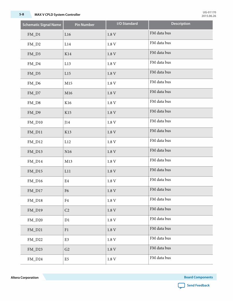
Schematic Signal Name Pin Number I/O Standard Description
FM_D1 L16 1.8 V FM data bus
FM_D2 L14 1.8 V FM data bus
FM_D3 K14 1.8 V FM data bus
FM_D4 L13 1.8 V FM data bus
FM_D5 L15 1.8 V FM data bus
FM_D6 M15 1.8 V FM data bus
FM_D7 M16 1.8 V FM data bus
FM_D8 K16 1.8 V FM data bus
FM_D9 K15 1.8 V FM data bus
FM_D10 J14 1.8 V FM data bus
FM_D11 K13 1.8 V FM data bus
FM_D12 L12 1.8 V FM data bus
FM_D13 N16 1.8 V FM data bus
FM_D14 M13 1.8 V FM data bus
FM_D15 L11 1.8 V FM data bus
FM_D16 E4 1.8 V FM data bus
FM_D17 F6 1.8 V FM data bus
FM_D18 F4 1.8 V FM data bus
FM_D19 C2 1.8 V FM data bus
FM_D20 D1 1.8 V FM data bus
FM_D21 F1 1.8 V FM data bus
FM_D22 E3 1.8 V FM data bus
FM_D23 G2 1.8 V FM data bus
FM_D24 E5 1.8 V FM data bus
5-8 MAX V CPLD System ControllerUG-01170
2015.06.26
Altera Corporation Board Components
Send Feedback

Schematic Signal Name Pin Number I/O Standard Description
FM_D25 C3 1.8 V FM data bus
FM_D26 D3 1.8 V FM data bus
FM_D27 D2 1.8 V FM data bus
FM_D28 E1 1.8 V FM data bus
FM_D29 G3 1.8 V FM data bus
FM_D30 F3 1.8 V FM data bus
FM_D31 F2 1.8 V FM data bus
FMCA_C2M_PG R16 1.8 V FMC port A power good output
FMCA_PRSNTN G1 1.8 V Green LED. Illuminates whenthe FMC port has a board orcable plugged-in. Driven by theadd-in card.
FMCB_C2M_PG L5 1.8 V FMC port B power good output
FMCB_PRSNTN E2 1.8 V Green LED. Illuminates whenthe FMC port has a board orcable plugged-in. Driven by theadd-in card.
FPGA_CONF_DONE
K1 1.8 V FPGA configuration done LED
FPGA_CONFIG_D0
R1 1.8 V FPGA configuration data
FPGA_CONFIG_D1
T2 1.8 V FPGA configuration data
FPGA_CONFIG_D2
N6 1.8 V FPGA configuration data
FPGA_CONFIG_D3
N5 1.8 V FPGA configuration data
FPGA_CONFIG_D4
N7 1.8 V FPGA configuration data
FPGA_CONFIG_D5
N8 1.8 V FPGA configuration data
UG-011702015.06.26 MAX V CPLD System Controller 5-9
Board Components Altera Corporation
Send Feedback

Schematic Signal Name Pin Number I/O Standard Description
FPGA_CONFIG_D6
M12 1.8 V FPGA configuration data
FPGA_CONFIG_D7
T13 1.8 V FPGA configuration data
FPGA_CONFIG_D8
T15 1.8 V FPGA configuration data
FPGA_CONFIG_D9
R13 1.8 V FPGA configuration data
FPGA_CONFIG_D10
P4 1.8 V FPGA configuration data
FPGA_CONFIG_D11
R3 1.8 V FPGA configuration data
FPGA_CONFIG_D12
T10 1.8 V FPGA configuration data
FPGA_CONFIG_D13
P5 1.8 V FPGA configuration data
FPGA_CONFIG_D14
R4 1.8 V FPGA configuration data
FPGA_CONFIG_D15
R5 1.8 V FPGA configuration data
FPGA_CONFIG_D16
M8 1.8 V FPGA configuration data
FPGA_CONFIG_D17
M7 1.8 V FPGA configuration data
FPGA_CONFIG_D18
T5 1.8 V FPGA configuration data
FPGA_CONFIG_D19
P9 1.8 V FPGA configuration data
FPGA_CONFIG_D20
M6 1.8 V FPGA configuration data
FPGA_CONFIG_D21
N9 1.8 V FPGA configuration data
5-10 MAX V CPLD System ControllerUG-01170
2015.06.26
Altera Corporation Board Components
Send Feedback

Schematic Signal Name Pin Number I/O Standard Description
FPGA_CONFIG_D22
R8 1.8 V FPGA configuration data
FPGA_CONFIG_D23
T8 1.8 V FPGA configuration data
FPGA_CONFIG_D24
P7 1.8 V FPGA configuration data
FPGA_CONFIG_D25
R7 1.8 V FPGA configuration data
FPGA_CONFIG_D26
R9 1.8 V FPGA configuration data
FPGA_CONFIG_D27
T9 1.8 V FPGA configuration data
FPGA_CONFIG_D28
T7 1.8 V FPGA configuration data
FPGA_CONFIG_D29
P8 1.8 V FPGA configuration data
FPGA_CONFIG_D30
R6 1.8 V FPGA configuration data
FPGA_CONFIG_D31
P6 1.8 V FPGA configuration data
FPGA_CVP_CONFDONE
M14 1.8 V FPGA Configuration viaProtocol (CvP) done
FPGA_DCLK M9 1.8 V FPGA configuration clock
FPGA_NCONFIG E14 1.8 V FPGA configuration active
FPGA_NSTATUS J4 1.8 V FPGA configuration ready
FPGA_PR_DONE H12 1.8 V FPGA partial reconfigurationdone
FPGA_PR_ERROR K12 1.8 V FPGA partial reconfigurationerror
FPGA_PR_READY P12 1.8 V FPGA partial reconfigurationready
FPGA_PR_REQUEST
T4 1.8 V FPGA partial reconfigurationrequest
UG-011702015.06.26 MAX V CPLD System Controller 5-11
Board Components Altera Corporation
Send Feedback
Schematic Signal Name Pin Number I/O Standard Description
M5_JTAG_TCK P3 1.8 V JTAG chain clock
M5_JTAG_TDI L6 1.8 V JTAG chain data in
M5_JTAG_TDO M5 1.8 V JTAG chain data out
M5_JTAG_TMS N4 1.8 V JTAG chain mode
MAX5_BEN0 R10 1.8 V MAX V Byte Enable 0
MAX5_BEN1 M10 1.8 V MAX V Byte Enable 1
MAX5_BEN2 T12 1.8 V MAX V Byte Enable 2
MAX5_BEN3 P10 1.8 V MAX V Byte Enable 3
MAX5_CLK N11 1.8 V MAX V Clock
MAX5_CSN T11 1.8 V MAX V chip select
MAX5_OEN N10 1.8 V MAX V output enable
MAX5_WEN R11 1.8 V MAX V Write enable
MAX_CONF_DONE
D7 2.5 V On-board USB-Blaster IIconfiguration done LED
MAX_ERROR C7 2.5 V FPGA configuration error LED
MAX_LOAD B6 2.5 V FPGA configuration active LED
MAX_RESETN J3 1.8 V MAX V reset push button
MSEL0 R12 1.8 V FPGA MSEL0 setting
MSEL1 P11 1.8 V FPGA MSEL1 setting
MSEL2 M11 1.8 V FPGA MSEL2 setting
MV_CLK_50 J12 1.8 V MAX V 50 MHz clock
OVERTEMP E11 2.5 V Temperature monitor fan enable
OVERTEMPN B16 2.5 V Temperature monitor fan enable
PGM_CONFIG A6 2.5 V Load the flash memory imageidentified by the PGM LEDs
5-12 MAX V CPLD System ControllerUG-01170
2015.06.26
Altera Corporation Board Components
Send Feedback

Schematic Signal Name Pin Number I/O Standard Description
PGM_LED0 D6 2.5 V Flash memory PGM selectindicator 0
PGM_LED1 C6 2.5 V Flash memory PGM selectindicator 1
PGM_LED2 B7 2.5 V Flash memory PGM selectindicator 2
PGM_SEL A7 2.5 V Toggles the PGM_LED[2:0] LEDsequence
SDI_MF0_BYPASS P13 1.8 V SDI Interface Mode Select 0 /Bypass control
SDI_MF1_AUTO_SLEEP
R14 1.8 V SDI Interface Mode Select 1 /Auto Sleep Control
SDI_MF2_MUTE N12 1.8 V SDI Interface Mode Select 2 /Output Mute
SDI_TX_SD_HDN N13 1.8 V SDI Interface TX Signal Detect
SENSE_CS0N D9 2.5 V SPI Interface Chip Select
SENSE_SCK B9 2.5 V SPI Interface Clock
SENSE_SDI B3 2.5 V SPI Interface Serial Data In
SENSE_SDO C9 2.5 V SPI Interface Serial Data Out
SENSE_SMB_CLK A15 2.5 V I2C Interface Clock
SENSE_SMB_DATA
B13 2.5 V I2C Interface Data
SI516_FS C5 2.5 V Silicon Labs SI516 Clock DeviceFrequency Select
SI570_EN A10 2.5 V Si570 programmable clockenable
TSENSE_ALERTN B14 2.5 V MAX1619 device TemperatureSense Alert Signal
USB_CFG0 M4 1.8 V On-board USB-Blaster IIinterface (reserved for futureuse)
USB_CFG1 M3 1.8 V On-board USB-Blaster IIinterface (reserved for futureuse)
UG-011702015.06.26 MAX V CPLD System Controller 5-13
Board Components Altera Corporation
Send Feedback

Schematic Signal Name Pin Number I/O Standard Description
USB_CFG2 K2 1.8 V On-board USB-Blaster IIinterface (reserved for futureuse)
USB_CFG3 K5 1.8 V On-board USB-Blaster IIinterface (reserved for futureuse)
USB_CFG4 L1 1.8 V On-board USB-Blaster IIinterface (reserved for futureuse)
USB_CFG5 L2 1.8 V On-board USB-Blaster IIinterface (reserved for futureuse)
USB_CFG6 K3 1.8 V On-board USB-Blaster IIinterface (reserved for futureuse)
USB_CFG7 M2 1.8 V On-board USB-Blaster IIinterface (reserved for futureuse)
USB_CFG8 L4 1.8 V On-board USB-Blaster IIinterface (reserved for futureuse)
USB_CFG9 L3 1.8 V On-board USB-Blaster IIinterface (reserved for futureuse)
USB_CFG10 N1 1.8 V On-board USB-Blaster IIinterface (reserved for futureuse)
USB_CFG11 N2 1.8 V On-board USB-Blaster IIinterface (reserved for futureuse)
USB_CFG12 M1 1.8 V On-board USB-Blaster IIinterface (reserved for futureuse)
USB_CFG13 N3 1.8 V On-board USB-Blaster IIinterface (reserved for futureuse)
USB_CFG14 P2 1.8 V On-board USB-Blaster IIinterface (reserved for futureuse)
USB_M5_CLK H5 1.8 V On-board USB-Blaster IIinterface clock
ED8101_ALERT B8 2.5 V ED8101 Alert signal
5-14 MAX V CPLD System ControllerUG-01170
2015.06.26
Altera Corporation Board Components
Send Feedback

Schematic Signal Name Pin Number I/O Standard Description
ED8101_SCL A8 2.5 V ED8101 I2C clock signal
ED8101_SDA A9 2.5 V ED8101 I2C data signal
FPGA Configuration
Configuring the FPGA Using ProgrammerYou can use the Quartus II Programmer to configure the FPGA with your SRAM Object File (.sof).
Ensure the following:
• The Quartus II Programmer and the USB-Blaster II driver are installed on the host computer.• The micro-USB cable is connected to the FPGA development board.• Power to the board is on, and no other applications that use the JTAG chain are running.
1. Start the Quartus II Programmer.2. Click Auto Detect to display the devices in the JTAG chain.3. Click Change File and select the path to the desired .sof.4. Turn on the Program/Configure option for the added file.5. Click Start to download the selected file to the FPGA. Configuration is complete when the progress
bar reaches 100%.
Using the Quartus II programmer to configure a device on the board causes other JTAG-basedapplications such as the Board Test System and the Power Monitor to lose their connection to the board.Restart those applications after configuration is complete.
Status ElementsThe Arria 10 GX FPGA development board includes status LEDs.
Table 5-3: Board-Specific LEDs
Board Reference Schematic Signal Name I/O Standard
D16 MAX_ERROR 2.5 V
D15 MAX_LOAD 2.5 V
D17 MAX_CONF_DONE 2.5 V
D1 FMCA_TX_LED 1.8 V
D2 FMCA_RX_LED 1.8 V
UG-011702015.06.26 FPGA Configuration 5-15
Board Components Altera Corporation
Send Feedback

Board Reference Schematic Signal Name I/O Standard
D12 PGM_LED0 2.5 V
D13 PGM_LED1 2.5 V
D14 PGM_LED2 2.5 V
D11 FMCA_PRSNTn 1.8 V
D18 FMCB_TX_LED 1.8 V
D20 FMCB_RX_LED 1.8 V
D21 FMCB_PRSNTn 1.8 V
D34 PCIE_LED_X1 1.8 V
D35 PCIE_LED_X4 1.8 V
D36 PCIE_LED_X8 1.8 V
D37 PCIE_LED_G2 1.8 V
D38 PCIE_LED_G3 1.8 V
5-16 Status ElementsUG-01170
2015.06.26
Altera Corporation Board Components
Send Feedback
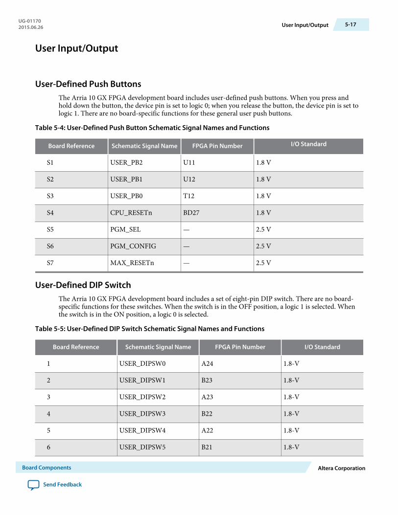
User Input/Output
User-Defined Push ButtonsThe Arria 10 GX FPGA development board includes user-defined push buttons. When you press andhold down the button, the device pin is set to logic 0; when you release the button, the device pin is set tologic 1. There are no board-specific functions for these general user push buttons.
Table 5-4: User-Defined Push Button Schematic Signal Names and Functions
Board Reference Schematic Signal Name FPGA Pin Number I/O Standard
S1 USER_PB2 U11 1.8 V
S2 USER_PB1 U12 1.8 V
S3 USER_PB0 T12 1.8 V
S4 CPU_RESETn BD27 1.8 V
S5 PGM_SEL — 2.5 V
S6 PGM_CONFIG — 2.5 V
S7 MAX_RESETn — 2.5 V
User-Defined DIP SwitchThe Arria 10 GX FPGA development board includes a set of eight-pin DIP switch. There are no board-specific functions for these switches. When the switch is in the OFF position, a logic 1 is selected. Whenthe switch is in the ON position, a logic 0 is selected.
Table 5-5: User-Defined DIP Switch Schematic Signal Names and Functions
Board Reference Schematic Signal Name FPGA Pin Number I/O Standard
1 USER_DIPSW0 A24 1.8-V
2 USER_DIPSW1 B23 1.8-V
3 USER_DIPSW2 A23 1.8-V
4 USER_DIPSW3 B22 1.8-V
5 USER_DIPSW4 A22 1.8-V
6 USER_DIPSW5 B21 1.8-V
UG-011702015.06.26 User Input/Output 5-17
Board Components Altera Corporation
Send Feedback

Board Reference Schematic Signal Name FPGA Pin Number I/O Standard
7 USER_DIPSW6 C21 1.8-V
8 USER_DIPSW7 A20 1.8-V
User-Defined LEDsThe Arria 10 GX FPGA development board includes a set of eight pairs user-defined LEDs. The LEDsilluminate when a logic 0 is driven, and turns off when a logic 1 is driven. There are no board-specificfunctions for these LEDs.
Table 5-6: User-Defined LEDs Schematic Signal Names and Functions
Board Reference Schematic Signal Name FPGA Pin Number I/O Standard
D10 USER_LED_G0 L28 1.8 VD9 USER_LED_G1 K26 1.8 VD8 USER_LED_G2 K25 1.8 VD7 USER_LED_G3 L25 1.8 VD6 USER_LED_G4 J24 1.8 VD5 USER_LED_G5 A19 1.8 VD4 USER_LED_G6 C18 1.8 VD3 USER_LED_G7 D18 1.8 VD10 USER_LED_R0 L27 1.8 VD9 USER_LED_R1 J26 1.8 VD8 USER_LED_R2 K24 1.8 VD7 USER_LED_R3 L23 1.8 VD6 USER_LED_R4 B20 1.8 VD5 USER_LED_R5 C19 1.8 VD4 USER_LED_R6 D19 1.8 VD3 USER_LED_R7 M23 1.8 V
Character LCDThe Arria 10 GX FPGA development board includes a single 10-pin 0.1" pitch single-row header thatinterfaces to a 16 character × 2 line Lumex LCD display. The LCD has a 10-pin receptacle that mountsdirectly to the board's 10-pin header, so it can be easily removed for access to components under thedisplay. You can also use the header for debugging or other purposes.
5-18 User-Defined LEDsUG-01170
2015.06.26
Altera Corporation Board Components
Send Feedback
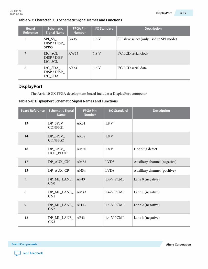
Table 5-7: Character LCD Schematic Signal Names and Functions
BoardReference
SchematicSignal Name
FPGA PinNumber
I/O Standard Description
5 SPI_SS_DISP / DISP_SPISS
BA35 1.8 V SPI slave select (only used in SPI mode)
7 I2C_SCL_DISP / DISP_I2C_SCL
AW33 1.8 V I2C LCD serial clock
8 I2C_SDA_DISP / DISP_I2C_SDA
AY34 1.8 V I2C LCD serial data
DisplayPortThe Arria 10 GX FPGA development board includes a DisplayPort connector.
Table 5-8: DisplayPort Schematic Signal Names and Functions
Board Reference Schematic SignalName
FPGA PinNumber
I/O Standard Description
13 DP_3P3V_CONFIG1
AK31 1.8 V
14 DP_3P3V_CONFIG2
AK32 1.8 V
18 DP_3P3V_HOT_PLUG
AM30 1.8 V Hot plug detect
17 DP_AUX_CN AM35 LVDS Auxiliary channel (negative)
15 DP_AUX_CP AN34 LVDS Auxiliary channel (positive)
3 DP_ML_LANE_CN0
AP43 1.4-V PCML Lane 0 (negative)
6 DP_ML_LANE_CN1
AM43 1.4-V PCML Lane 1 (negative)
9 DP_ML_LANE_CN2
AH43 1.4-V PCML Lane 2 (negative)
12 DP_ML_LANE_CN3
AF43 1.4-V PCML Lane 3 (negative)
UG-011702015.06.26 DisplayPort 5-19
Board Components Altera Corporation
Send Feedback
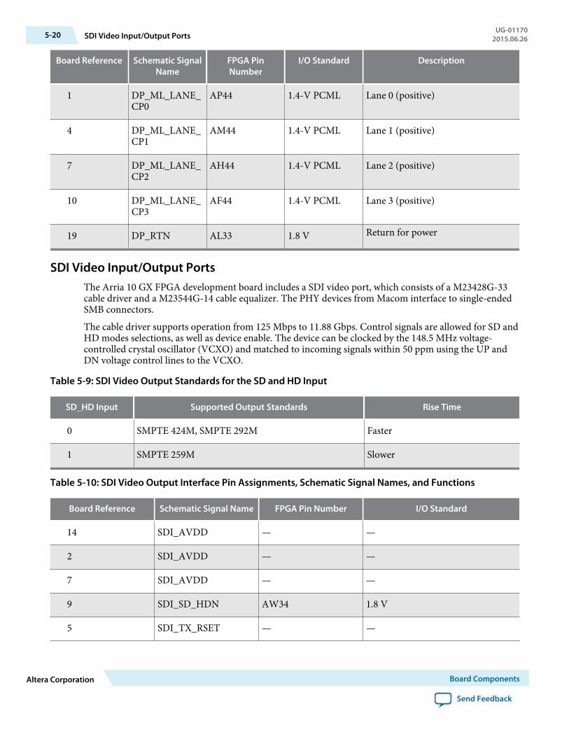
Board Reference Schematic SignalName
FPGA PinNumber
I/O Standard Description
1 DP_ML_LANE_CP0
AP44 1.4-V PCML Lane 0 (positive)
4 DP_ML_LANE_CP1
AM44 1.4-V PCML Lane 1 (positive)
7 DP_ML_LANE_CP2
AH44 1.4-V PCML Lane 2 (positive)
10 DP_ML_LANE_CP3
AF44 1.4-V PCML Lane 3 (positive)
19 DP_RTN AL33 1.8 V Return for power
SDI Video Input/Output PortsThe Arria 10 GX FPGA development board includes a SDI video port, which consists of a M23428G-33cable driver and a M23544G-14 cable equalizer. The PHY devices from Macom interface to single-endedSMB connectors.
The cable driver supports operation from 125 Mbps to 11.88 Gbps. Control signals are allowed for SD andHD modes selections, as well as device enable. The device can be clocked by the 148.5 MHz voltage-controlled crystal oscillator (VCXO) and matched to incoming signals within 50 ppm using the UP andDN voltage control lines to the VCXO.
Table 5-9: SDI Video Output Standards for the SD and HD Input
SD_HD Input Supported Output Standards Rise Time
0 SMPTE 424M, SMPTE 292M Faster
1 SMPTE 259M Slower
Table 5-10: SDI Video Output Interface Pin Assignments, Schematic Signal Names, and Functions
Board Reference Schematic Signal Name FPGA Pin Number I/O Standard
14 SDI_AVDD — —
2 SDI_AVDD — —
7 SDI_AVDD — —
9 SDI_SD_HDN AW34 1.8 V
5 SDI_TX_RSET — —
5-20 SDI Video Input/Output PortsUG-01170
2015.06.26
Altera Corporation Board Components
Send Feedback

Board Reference Schematic Signal Name FPGA Pin Number I/O Standard
1 SDI_TXCAP_N D43 1.4-V PCML
16 SDI_TXCAP_P D44 1.4-V PCML
10 SDI_TXDRV_N — —
11 SDI_TXDRV_P — —
Table 5-11: SDI Cable Equalizer Lengths
The cable equalizer supports operation at 270 Mbit SD, 1.5 Gbit HD, and 3.0, 6.0, and 11.88 Gbit dual-link HDmodes. Control signals are allowed for bypassing or disabling the device, as well as a carrier detect or auto-mutesignal interface.
Cable Type Data Rate (Mbps) Maximum Cable Length (m)
Belden 1694A 270 400
Belden 1694A 1485 140
Belden 1694A 2970 120
Table 5-12: SDI Video Input Interface Pin Assignments, Schematic Signal Names, and Functions
Board Reference Schematic Signal Name FPGA Pin Number I/O Standard
9 AGCN — —
8 AGXP — —
10 MF0_BYPASS AW32 1.8 V
19 MF1_AUTO_SLEEP AY32 1.8 V
21 MF2_MUTE AY35 1.8 V
22 MF3_XSD — —
6 MODE_SEL — —
11 MUTEREF — —
4 SDI_EQIN_N1 — —
3 SDI_EQIN_P1 — —
14 SDO_N / SDI_RX_N H39 1.4-V PCML
UG-011702015.06.26 SDI Video Input/Output Ports 5-21
Board Components Altera Corporation
Send Feedback
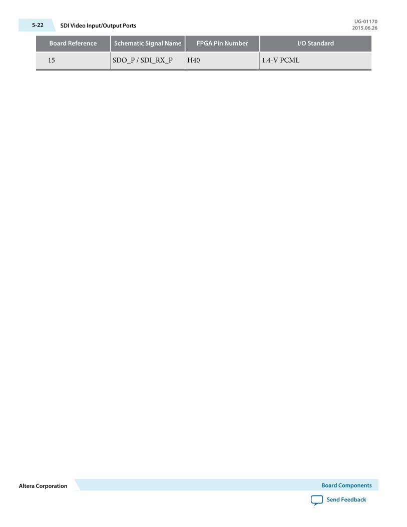
Board Reference Schematic Signal Name FPGA Pin Number I/O Standard
15 SDO_P / SDI_RX_P H40 1.4-V PCML
5-22 SDI Video Input/Output PortsUG-01170
2015.06.26
Altera Corporation Board Components
Send Feedback

Clock Circuitry
On-Board Oscillators
Figure 5-2: Arria 10 GX FPGA Kit Board Clock Inputs and Default Frequencies
B 2A
B 3A
B 2L
B 3H
1C 1D 1E 1F 1G 1H
4D 4E 4F 4G 4H 4I
Bank 3
Bank 2
Si 5338
CLK 0
CLK 1
CLK 2
CLK 3
SL 18860Buffer CLK _50
MV _CLK _50
125 M
Buffer 2:6Si 53301 /Si 53311100 MHz Default
100 M_P /N
REFCLK 4_P /N
SMA
50M
PCIE _OB _REFCLK _P /N
PCIE
_ED
GE
_REF
CLK
_P/N
REFC
LK_D
P_P
/N
REFC
LK_S
FP_P
/N
REFC
LK_Q
SFP
_P/N
REFC
LK_S
DI_
P/N
REFC
LK_F
MCA
_P/N
REFC
LK_F
MCB
_P/N
REFC
LK_S
MA
_P/N
CLK _125 M_P /N
Si 5338
CLK 0
CLK 1
CLK 2
CLK 3
CLK _EMI _P /N
133 .33MHz
644 .53125 MHz
644 .53125 MHz
270 MHz
Si 516 /Si 571
100 MHz
625 MHz
625 MHz
348 MHzSi570
FMCA
_GBT
CLK
_M2C
_P0/
N0
FMCA
_GBT
CLK
_M2C
_P1/
N1
FMCB
_GBT
CLK
_M2C
_P0/
N0
FMCB
_GBT
CLK
_M2C
_P1/
N1 REFCLK 1_P /N
CLK _FPGA _B 3_P /N
REFC
LK1_
P/N
CLK _FPGA _B 2_P /N
SMA
Arria 10GX
UG-011702015.06.26 Clock Circuitry 5-23
Board Components Altera Corporation
Send Feedback

Table 5-13: On-Board Oscillators
Source Schematic Signal Name Frequency I/O Standard Arria 10FPGA PinNumber
Application
U14
REFCLK_SMA_P 302.083333MHz
1.8 V LVDS N37 Transceiver referenceclocks Bank-1HREFCLK_SMA_N 1.8 V LVDS N38
REFCLK_FMCB_P625 MHz
1.8 V LVDS AA8 FMC B referenceclocksREFCLK_FMCB_N 1.8 V LVDS AA7
REFCLK_FMCA_P625 MHz
1.8 V LVDS AN8 FMC A referenceclocksREFCLK_FMCA_N 1.8 V LVDS AN7
PCIE_OB_REFCLK_P100 MHz
1.8 V LVDS AN37PCIE reference clocks
PCIE_OB_REFCLK_N 1.8 V LVDS AN38
U26
CLK_EMI_P133.33 MHz
1.8 V LVDS F34EMI reference clocks
CLK_EMI_N 1.8 V LVDS F35REFCLK_QSFP_P 644.53125
MHz1.8 V LVDS R37
QSFP reference clocksREFCLK_QSFP_N 1.8 V LVDS R38REFCLK_SFP_P 644.53125
MHz1.8 V LVDS AA37
SFP reference clocksREFCLK_SFP_N 1.8 V LVDS AA38REFCLK_DP_P
270 MHz1.8 V LVDS AC37 Display port (DP)
reference clocksREFCLK_DP_N 1.8 V LVDS AC38
X1REFCLK_SDI_P
148.35 MHz2.5 V L37
SDI reference clocksREFCLK_SDI_N 2.5 V L38
X2CLK_125_P
125 MHz2.5 V BD25 125 MHz reference
clocks for Arria 10FPGACLK_125_N 2.5 V BC24
X3100M_OSC_P
100 MHz2.5 V - Programmable
Oscillator default100MHz100M_OSC_N 2.5 V -
U53
MV_CLK_50
50 MHz
1.8 V - MAX V SystemController clock
CLK_50 1.8 V AU33 Arria 10 FPGAreference clock
Off-Board Clock I/OThe development board has input and output clocks which can be driven onto the board. The outputclocks can be programmed to different levels and I/O standards according to the FPGA device’s specifica‐tion.
5-24 Off-Board Clock I/OUG-01170
2015.06.26
Altera Corporation Board Components
Send Feedback
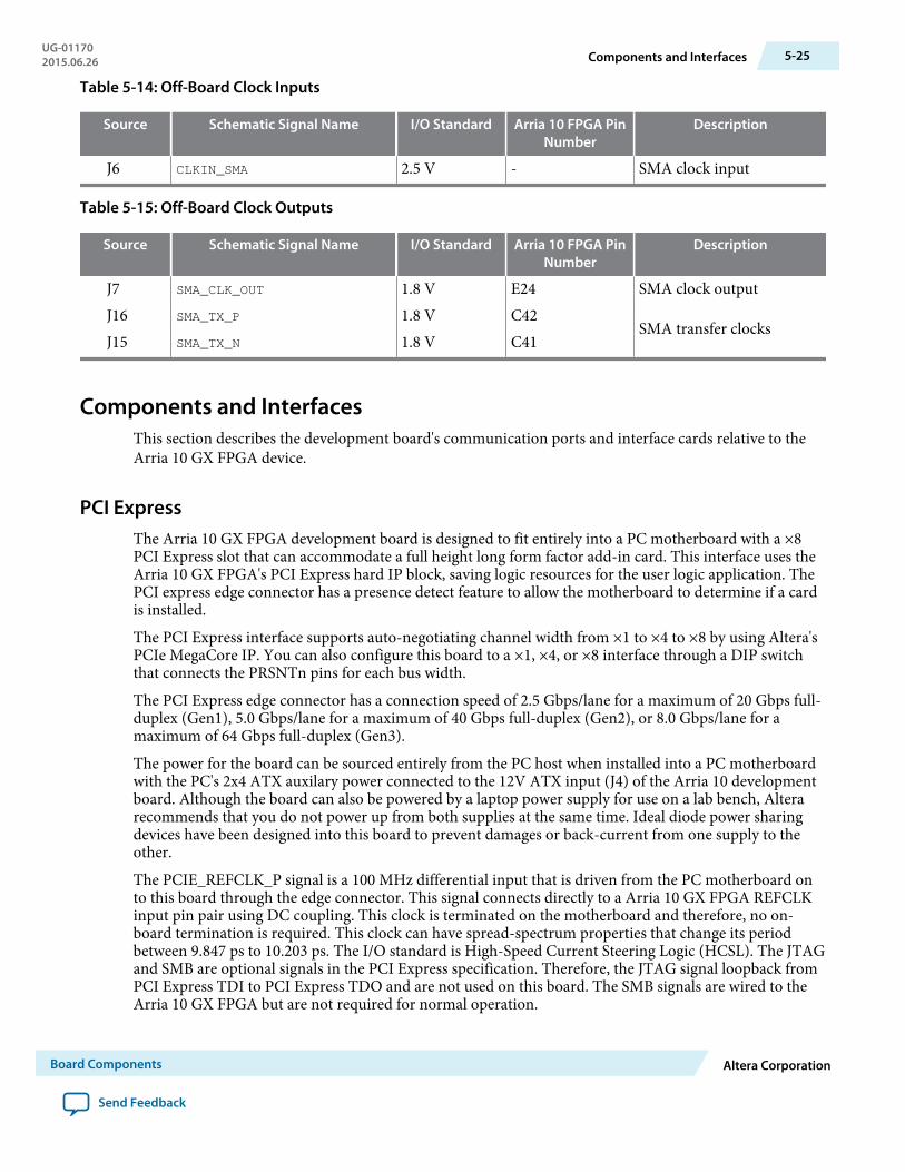
Table 5-14: Off-Board Clock Inputs
Source Schematic Signal Name I/O Standard Arria 10 FPGA PinNumber
Description
J6 CLKIN_SMA 2.5 V - SMA clock input
Table 5-15: Off-Board Clock Outputs
Source Schematic Signal Name I/O Standard Arria 10 FPGA PinNumber
Description
J7 SMA_CLK_OUT 1.8 V E24 SMA clock outputJ16 SMA_TX_P 1.8 V C42
SMA transfer clocksJ15 SMA_TX_N 1.8 V C41
Components and InterfacesThis section describes the development board's communication ports and interface cards relative to theArria 10 GX FPGA device.
PCI ExpressThe Arria 10 GX FPGA development board is designed to fit entirely into a PC motherboard with a ×8PCI Express slot that can accommodate a full height long form factor add-in card. This interface uses theArria 10 GX FPGA's PCI Express hard IP block, saving logic resources for the user logic application. ThePCI express edge connector has a presence detect feature to allow the motherboard to determine if a cardis installed.
The PCI Express interface supports auto-negotiating channel width from ×1 to ×4 to ×8 by using Altera'sPCIe MegaCore IP. You can also configure this board to a ×1, ×4, or ×8 interface through a DIP switchthat connects the PRSNTn pins for each bus width.
The PCI Express edge connector has a connection speed of 2.5 Gbps/lane for a maximum of 20 Gbps full-duplex (Gen1), 5.0 Gbps/lane for a maximum of 40 Gbps full-duplex (Gen2), or 8.0 Gbps/lane for amaximum of 64 Gbps full-duplex (Gen3).
The power for the board can be sourced entirely from the PC host when installed into a PC motherboardwith the PC's 2x4 ATX auxilary power connected to the 12V ATX input (J4) of the Arria 10 developmentboard. Although the board can also be powered by a laptop power supply for use on a lab bench, Alterarecommends that you do not power up from both supplies at the same time. Ideal diode power sharingdevices have been designed into this board to prevent damages or back-current from one supply to theother.
The PCIE_REFCLK_P signal is a 100 MHz differential input that is driven from the PC motherboard onto this board through the edge connector. This signal connects directly to a Arria 10 GX FPGA REFCLKinput pin pair using DC coupling. This clock is terminated on the motherboard and therefore, no on-board termination is required. This clock can have spread-spectrum properties that change its periodbetween 9.847 ps to 10.203 ps. The I/O standard is High-Speed Current Steering Logic (HCSL). The JTAGand SMB are optional signals in the PCI Express specification. Therefore, the JTAG signal loopback fromPCI Express TDI to PCI Express TDO and are not used on this board. The SMB signals are wired to theArria 10 GX FPGA but are not required for normal operation.
UG-011702015.06.26 Components and Interfaces 5-25
Board Components Altera Corporation
Send Feedback
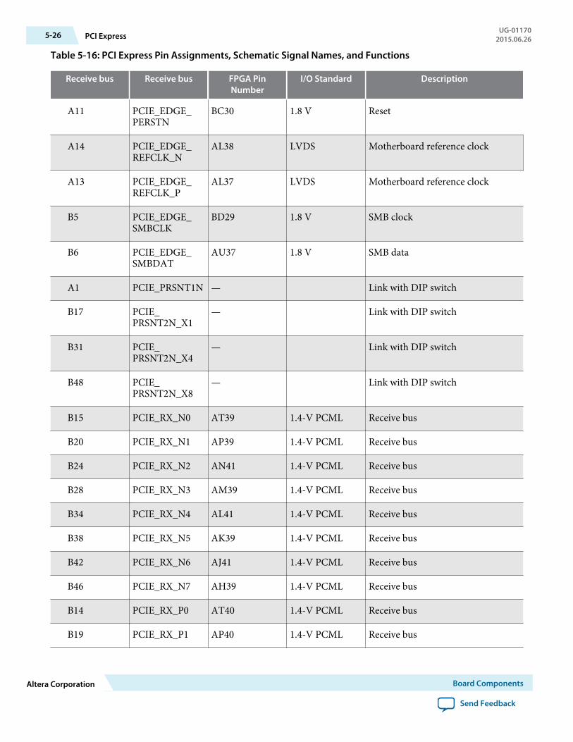
Table 5-16: PCI Express Pin Assignments, Schematic Signal Names, and Functions
Receive bus Receive bus FPGA PinNumber
I/O Standard Description
A11 PCIE_EDGE_PERSTN
BC30 1.8 V Reset
A14 PCIE_EDGE_REFCLK_N
AL38 LVDS Motherboard reference clock
A13 PCIE_EDGE_REFCLK_P
AL37 LVDS Motherboard reference clock
B5 PCIE_EDGE_SMBCLK
BD29 1.8 V SMB clock
B6 PCIE_EDGE_SMBDAT
AU37 1.8 V SMB data
A1 PCIE_PRSNT1N — Link with DIP switch
B17 PCIE_PRSNT2N_X1
— Link with DIP switch
B31 PCIE_PRSNT2N_X4
— Link with DIP switch
B48 PCIE_PRSNT2N_X8
— Link with DIP switch
B15 PCIE_RX_N0 AT39 1.4-V PCML Receive bus
B20 PCIE_RX_N1 AP39 1.4-V PCML Receive bus
B24 PCIE_RX_N2 AN41 1.4-V PCML Receive bus
B28 PCIE_RX_N3 AM39 1.4-V PCML Receive bus
B34 PCIE_RX_N4 AL41 1.4-V PCML Receive bus
B38 PCIE_RX_N5 AK39 1.4-V PCML Receive bus
B42 PCIE_RX_N6 AJ41 1.4-V PCML Receive bus
B46 PCIE_RX_N7 AH39 1.4-V PCML Receive bus
B14 PCIE_RX_P0 AT40 1.4-V PCML Receive bus
B19 PCIE_RX_P1 AP40 1.4-V PCML Receive bus
5-26 PCI ExpressUG-01170
2015.06.26
Altera Corporation Board Components
Send Feedback

Receive bus Receive bus FPGA PinNumber
I/O Standard Description
B23 PCIE_RX_P2 AN42 1.4-V PCML Receive bus
B27 PCIE_RX_P3 AM40 1.4-V PCML Receive bus
B33 PCIE_RX_P4 AL42 1.4-V PCML Receive bus
B37 PCIE_RX_P5 AK40 1.4-V PCML Receive bus
B41 PCIE_RX_P6 AJ42 1.4-V PCML Receive bus
B45 PCIE_RX_P7 AH40 1.4-V PCML Receive bus
A17 PCIE_TX_CN0 BB43 1.4-V PCML Transmit bus
A22 PCIE_TX_CN1 BA41 1.4-V PCML Transmit bus
A26 PCIE_TX_CN2 AY43 1.4-V PCML Transmit bus
A30 PCIE_TX_CN3 AW41 1.4-V PCML Transmit bus
A36 PCIE_TX_CN4 AV43 1.4-V PCML Transmit bus
A40 PCIE_TX_CN5 AU41 1.4-V PCML Transmit bus
A44 PCIE_TX_CN6 AT43 1.4-V PCML Transmit bus
A48 PCIE_TX_CN7 AR41 1.4-V PCML Transmit bus
A16 PCIE_TX_CP0 BB44 1.4-V PCML Transmit bus
A21 PCIE_TX_CP1 BA42 1.4-V PCML Transmit bus
A25 PCIE_TX_CP2 AY44 1.4-V PCML Transmit bus
A29 PCIE_TX_CP3 AW42 1.4-V PCML Transmit bus
A35 PCIE_TX_CP4 AV44 1.4-V PCML Transmit bus
A39 PCIE_TX_CP5 AU42 1.4-V PCML Transmit bus
A43 PCIE_TX_CP6 AT44 1.4-V PCML Transmit bus
A47 PCIE_TX_CP7 AR42 1.4-V PCML Transmit bus
B11 PCIE_WAKEN_R
AY29 1.8 V Wake signal
UG-011702015.06.26 PCI Express 5-27
Board Components Altera Corporation
Send Feedback

10/100/1000 Ethernet PHYThe Arria 10 GX FPGA development board supports 10/100/1000 base-T Ethernet using an externalMarvell 88E1111 PHY and Altera Triple-Speed Ethernet MegaCore MAC function. The PHY-to-MACinterface employs SGMII using the Arria 10 GX FPGA LVDS pins in Soft-CDR mode at 1.25 Gbpstransmit and receive. In 10-Mb or 100-Mb mode, the SGMII interface still runs at 1.25 GHz but thepacket data is repeated 10 or 100 times. The MAC function must be provided in the FPGA for typicalnetworking applications.
The Marvell 88E1111 PHY uses 2.5-V and 1.0-V power rails and requires a 25 MHz reference clock drivenfrom a dedicated oscillator. The PHY interfaces to a HALO HFJ11-1G02E model RJ45 with internalmagnetics that can be used for driving copper lines with Ethernet traffic.
Table 5-17: Ethernet PHY Pin Assignments, Signal Names and Functions
Board Reference(U15)
Schematic SignalName
FPGA PinNumber
I/O Standard Description
23 ENET_2P5V_INTN
AG13 1.8 V Management bus interrupt
25 ENET_2P5V_MDC
AF13 1.8 V Management bus data clock
24 ENET_2P5V_MDIO
AL18 1.8 V Management bus data
28 ENET_2P5V_RESETN
AW23 1.8 V Device reset
59 ENET_LED_LINK10
— 2.5 V 10-Mb link LED
76 ENET_LED_LINK10
— 2.5 V 10-Mb link LED
74 ENET_LED_LINK100
— 2.5 V 100-Mb link LED
60 ENET_LED_LINK1000
— 2.5 V 1000-Mb link LED
73 ENET_LED_LINK1000
— 2.5 V 1000-Mb link LED
58 ENET_LED_RX — 2.5 V RX data active LED
69 ENET_LED_RX — 2.5 V RX data active LED
68 ENET_LED_TX — 2.5 V TX data active LED
5-28 10/100/1000 Ethernet PHYUG-01170
2015.06.26
Altera Corporation Board Components
Send Feedback
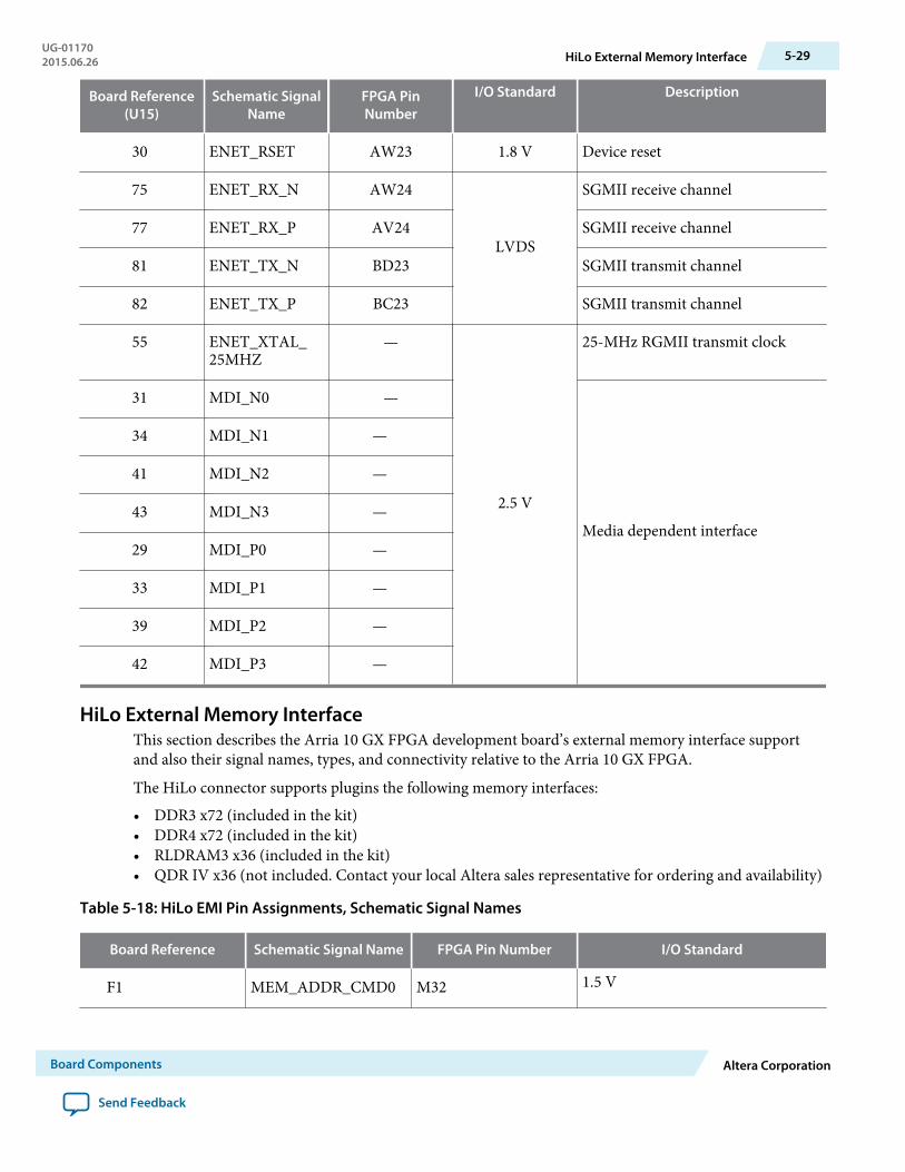
Board Reference(U15)
Schematic SignalName
FPGA PinNumber
I/O Standard Description
30 ENET_RSET AW23 1.8 V Device reset
75 ENET_RX_N AW24
LVDS
SGMII receive channel
77 ENET_RX_P AV24 SGMII receive channel
81 ENET_TX_N BD23 SGMII transmit channel
82 ENET_TX_P BC23 SGMII transmit channel
55 ENET_XTAL_25MHZ
—
2.5 V
25-MHz RGMII transmit clock
31 MDI_N0 —
Media dependent interface
34 MDI_N1 —
41 MDI_N2 —
43 MDI_N3 —
29 MDI_P0 —
33 MDI_P1 —
39 MDI_P2 —
42 MDI_P3 —
HiLo External Memory InterfaceThis section describes the Arria 10 GX FPGA development board’s external memory interface supportand also their signal names, types, and connectivity relative to the Arria 10 GX FPGA.
The HiLo connector supports plugins the following memory interfaces:
• DDR3 x72 (included in the kit)• DDR4 x72 (included in the kit)• RLDRAM3 x36 (included in the kit)• QDR IV x36 (not included. Contact your local Altera sales representative for ordering and availability)
Table 5-18: HiLo EMI Pin Assignments, Schematic Signal Names
Board Reference Schematic Signal Name FPGA Pin Number I/O Standard
F1 MEM_ADDR_CMD0 M32 1.5 V
UG-011702015.06.26 HiLo External Memory Interface 5-29
Board Components Altera Corporation
Send Feedback

Board Reference Schematic Signal Name FPGA Pin Number I/O Standard
H1 MEM_ADDR_CMD1 L32 1.5 V
F2 MEM_ADDR_CMD2 N34 1.5 V
G2 MEM_ADDR_CMD3 M35 1.5 V
H2 MEM_ADDR_CMD4 L34 1.5 V
J2 MEM_ADDR_CMD5 K34 1.5 V
K2 MEM_ADDR_CMD6 M33 1.5 V
G3 MEM_ADDR_CMD7 L33 1.5V
J3 MEM_ADDR_CMD8 J33 1.5 V
L3 MEM_ADDR_CMD9 J32 1.5 V
E4 MEM_ADDR_CMD10 H31 1.5 V
F4 MEM_ADDR_CMD11 J31 1.5 V
G4 MEM_ADDR_CMD12 H34 1.5 V
H4 MEM_ADDR_CMD13 H33 1.5 V
J4 MEM_ADDR_CMD14 G32 1.5 V
K4 MEM_ADDR_CMD15 E32 1.5 V
M1 MEM_ADDR_CMD16 F33 1.5 V
M2 MEM_ADDR_CMD17 G35 1.5 V
N2 MEM_ADDR_CMD18 H35 1.5 V
L4 MEM_ADDR_CMD19 G33 1.5 V
P5 MEM_ADDR_CMD20 U33 1.5 V
M5 MEM_ADDR_CMD21 T33 1.5 V
P1 MEM_ADDR_CMD22 R34 1.5 V
R4 MEM_ADDR_CMD23 P34 1.5 V
M4 MEM_ADDR_CMD24 N33 1.5 V
5-30 HiLo External Memory InterfaceUG-01170
2015.06.26
Altera Corporation Board Components
Send Feedback
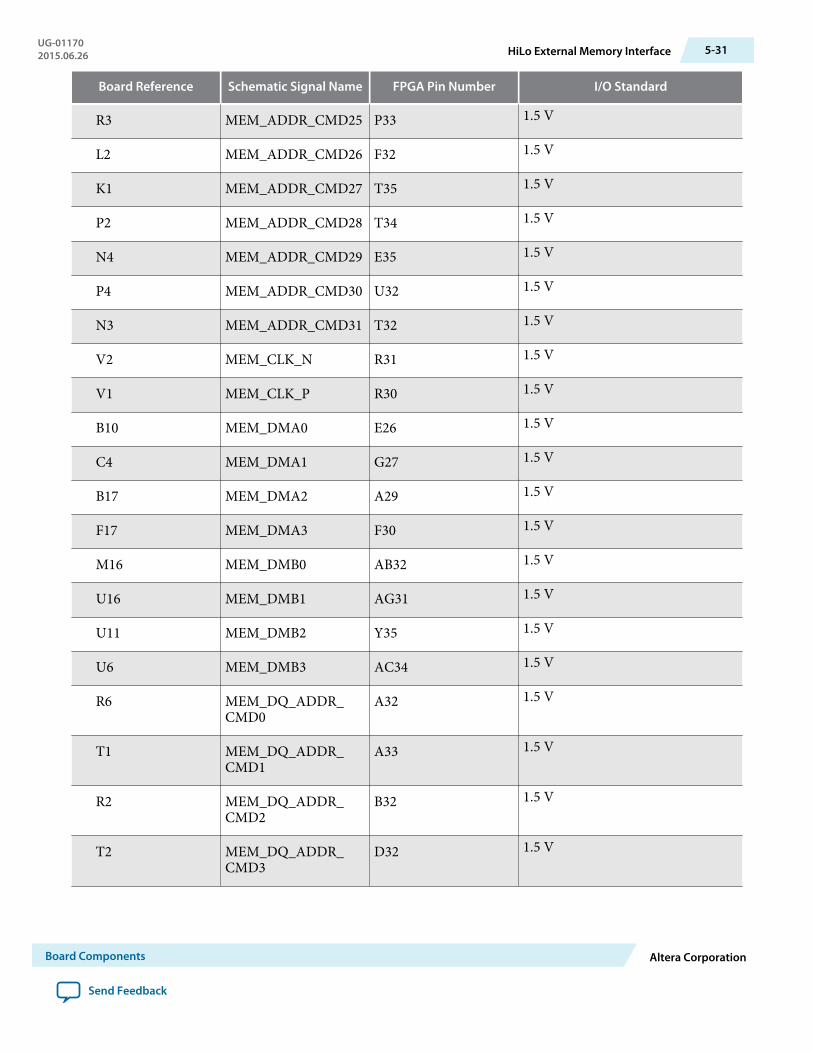
Board Reference Schematic Signal Name FPGA Pin Number I/O Standard
R3 MEM_ADDR_CMD25 P33 1.5 V
L2 MEM_ADDR_CMD26 F32 1.5 V
K1 MEM_ADDR_CMD27 T35 1.5 V
P2 MEM_ADDR_CMD28 T34 1.5 V
N4 MEM_ADDR_CMD29 E35 1.5 V
P4 MEM_ADDR_CMD30 U32 1.5 V
N3 MEM_ADDR_CMD31 T32 1.5 V
V2 MEM_CLK_N R31 1.5 V
V1 MEM_CLK_P R30 1.5 V
B10 MEM_DMA0 E26 1.5 V
C4 MEM_DMA1 G27 1.5 V
B17 MEM_DMA2 A29 1.5 V
F17 MEM_DMA3 F30 1.5 V
M16 MEM_DMB0 AB32 1.5 V
U16 MEM_DMB1 AG31 1.5 V
U11 MEM_DMB2 Y35 1.5 V
U6 MEM_DMB3 AC34 1.5 V
R6 MEM_DQ_ADDR_CMD0
A32 1.5 V
T1 MEM_DQ_ADDR_CMD1
A33 1.5 V
R2 MEM_DQ_ADDR_CMD2
B32 1.5 V
T2 MEM_DQ_ADDR_CMD3
D32 1.5 V
UG-011702015.06.26 HiLo External Memory Interface 5-31
Board Components Altera Corporation
Send Feedback

Board Reference Schematic Signal Name FPGA Pin Number I/O Standard
U2 MEM_DQ_ADDR_CMD4
C33 1.5 V
U3 MEM_DQ_ADDR_CMD5
B33 1.5 V
T4 MEM_DQ_ADDR_CMD6
D34 1.5 V
U4 MEM_DQ_ADDR_CMD7
C35 1.5 V
T5 MEM_DQ_ADDR_CMD8
E34 1.5 V
A4 MEM_DQA0 B28 1.5 V
B4 MEM_DQA1 A28 1.5 V
B5 MEM_DQA2 A27 1.5 V
B6 MEM_DQA3 B27 1.5 V
A8 MEM_DQA4 D27 1.5 V
B8 MEM_DQA5 E27 1.5 V
B9 MEM_DQA6 D26 1.5 V
A10 MEM_DQA7 D28 1.5 V
B1 MEM_DQA8 G25 1.5 V
B2 MEM_DQA9 H25 1.5 V
C2 MEM_DQA10 G26 1.5 V
C3 MEM_DQA11 H26 1.5 V
E3 MEM_DQA12 G28 1.5 V
D4 MEM_DQA13 F27 1.5 V
D1 MEM_DQA14 K27 1.5 V
D2 MEM_DQA15 F28 1.5 V
5-32 HiLo External Memory InterfaceUG-01170
2015.06.26
Altera Corporation Board Components
Send Feedback

Board Reference Schematic Signal Name FPGA Pin Number I/O Standard
A12 MEM_DQA16 D31 1.5 V
B12 MEM_DQA17 E31 1.5 V
B13 MEM_DQA18 B31 1.5 V
B14 MEM_DQA19 C31 1.5 V
C15 MEM_DQA20 A30 1.5 V
A16 MEM_DQA21 E30 1.5 V
B16 MEM_DQA22 B30 1.5 V
A18 MEM_DQA23 D29 1.5 V
C16 MEM_DQA24 K30 1.5 V
D16 MEM_DQA25 H30 1.5 V
E16 MEM_DQA26 G30 1.5 V
F16 MEM_DQA27 K31 1.5 V
D17 MEM_DQA28 H29 1.5 V
C18 MEM_DQA29 K29 1.5 V
D18 MEM_DQA30 J29 1.5 V
E18 MEM_DQA31 F29 1.5 V
E2 MEM_DQA32 J28 1.5 V
G16 MEM_DQA33 G31 1.5 V
H16 MEM_DQB0 AC31 1.5 V
J16 MEM_DQB1 AB31 1.5 V
K16 MEM_DQB2 W31 1.5 V
L16 MEM_DQB3 Y31 1.5 V
H17 MEM_DQB4 AD31 1.5 V
K17 MEM_DQB5 AD32 1.5 V
UG-011702015.06.26 HiLo External Memory Interface 5-33
Board Components Altera Corporation
Send Feedback

Board Reference Schematic Signal Name FPGA Pin Number I/O Standard
K18 MEM_DQB6 AD33 1.5 V
L18 MEM_DQB7 AA30 1.5 V
M17 MEM_DQB8 AE31 1.5 V
N18 MEM_DQB9 AE32 1.5 V
P17 MEM_DQB10 AE30 1.5 V
P18 MEM_DQB11 AF30 1.5 V
R18 MEM_DQB12 AG33 1.5 V
T16 MEM_DQB13 AG32 1.5 V
T17 MEM_DQB14 AH33 1.5 V
T18 MEM_DQB15 AH31 1.5 V
U15 MEM_DQB16 U31 1.5 V
T14 MEM_DQB17 W33 1.5 V
U14 MEM_DQB18 W32 1.5 V
V14 MEM_DQB19 V31 1.5 V
T13 MEM_DQB20 Y34 1.5 V
T12 MEM_DQB21 W35 1.5 V
U12 MEM_DQB22 W34 1.5 V
V12 MEM_DQB23 V34 1.5 V
T10 MEM_DQB24 AH35 1.5 V
U10 MEM_DQB25 AJ34 1.5 V
V10 MEM_DQB26 AJ33 1.5 V
T9 MEM_DQB27 AH34 1.5 V
T8 MEM_DQB28 AD35 1.5 V
U8 MEM_DQB29 AE34 1.5 V
5-34 HiLo External Memory InterfaceUG-01170
2015.06.26
Altera Corporation Board Components
Send Feedback

Board Reference Schematic Signal Name FPGA Pin Number I/O Standard
U7 MEM_DQB30 AC33 1.5 V
V6 MEM_DQB31 AD34 1.5 V
R16 MEM_DQB32 AF32 1.5 V
T6 MEM_DQB33 AB33 1.5 V
V5 MEM_DQS_ADDR_CMD_N
C34 1.5 V
V4 MEM_DQS_ADDR_CMD_P
D33 1.5 V
A7 MEM_DQSA_N0 C26 1.5 V
A3 MEM_DQSA_N1 J27 1.5 V
A15 MEM_DQSA_N2 C29 1.5 V
G18 MEM_DQSA_N3 L29 1.5 V
A6 MEM_DQSA_P0 B26 1.5 V
A2 MEM_DQSA_P1 H28 1.5 V
A14 MEM_DQSA_P2 C30 1.5 V
F18 MEM_DQSA_P3 L30 1.5 V
J18 MEM_DQSB_N0 AA32 1.5 V
V18 MEM_DQSB_N1 AJ31 1.5 V
V17 MEM_DQSB_N2 AA33 1.5 V
V9 MEM_DQSB_N3 AF34 1.5 V
H18 MEM_DQSB_P0 Y32 1.5 V
U18 MEM_DQSB_P1 AJ32 1.5 V
V16 MEM_DQSB_P2 AA34 1.5 V
V8 MEM_DQSB_P3 AF33 1.5 V
A11 MEM_QKA_P0 C28 1.5 V
UG-011702015.06.26 HiLo External Memory Interface 5-35
Board Components Altera Corporation
Send Feedback
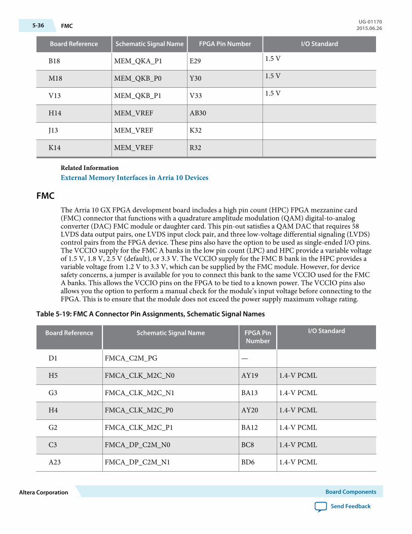
Board Reference Schematic Signal Name FPGA Pin Number I/O Standard
B18 MEM_QKA_P1 E29 1.5 V
M18 MEM_QKB_P0 Y30 1.5 V
V13 MEM_QKB_P1 V33 1.5 V
H14 MEM_VREF AB30
J13 MEM_VREF K32
K14 MEM_VREF R32
Related InformationExternal Memory Interfaces in Arria 10 Devices
FMCThe Arria 10 GX FPGA development board includes a high pin count (HPC) FPGA mezzanine card(FMC) connector that functions with a quadrature amplitude modulation (QAM) digital-to-analogconverter (DAC) FMC module or daughter card. This pin-out satisfies a QAM DAC that requires 58LVDS data output pairs, one LVDS input clock pair, and three low-voltage differential signaling (LVDS)control pairs from the FPGA device. These pins also have the option to be used as single-ended I/O pins.The VCCIO supply for the FMC A banks in the low pin count (LPC) and HPC provide a variable voltageof 1.5 V, 1.8 V, 2.5 V (default), or 3.3 V. The VCCIO supply for the FMC B bank in the HPC provides avariable voltage from 1.2 V to 3.3 V, which can be supplied by the FMC module. However, for devicesafety concerns, a jumper is available for you to connect this bank to the same VCCIO used for the FMCA banks. This allows the VCCIO pins on the FPGA to be tied to a known power. The VCCIO pins alsoallows you the option to perform a manual check for the module’s input voltage before connecting to theFPGA. This is to ensure that the module does not exceed the power supply maximum voltage rating.
Table 5-19: FMC A Connector Pin Assignments, Schematic Signal Names
Board Reference Schematic Signal Name FPGA PinNumber
I/O Standard
D1 FMCA_C2M_PG —
H5 FMCA_CLK_M2C_N0 AY19 1.4-V PCML
G3 FMCA_CLK_M2C_N1 BA13 1.4-V PCML
H4 FMCA_CLK_M2C_P0 AY20 1.4-V PCML
G2 FMCA_CLK_M2C_P1 BA12 1.4-V PCML
C3 FMCA_DP_C2M_N0 BC8 1.4-V PCML
A23 FMCA_DP_C2M_N1 BD6 1.4-V PCML
5-36 FMCUG-01170
2015.06.26
Altera Corporation Board Components
Send Feedback

Board Reference Schematic Signal Name FPGA PinNumber
I/O Standard
A27 FMCA_DP_C2M_N2 BB6 1.4-V PCML
A31 FMCA_DP_C2M_N3 BC4 1.4-V PCML
A35 FMCA_DP_C2M_N4 BB2 1.4-V PCML
A39 FMCA_DP_C2M_N5 BA4 1.4-V PCML
B37 FMCA_DP_C2M_N6 AY2 1.4-V PCML
B33 FMCA_DP_C2M_N7 AW4 1.4-V PCML
B29 FMCA_DP_C2M_N8 AV2 1.4-V PCML
B25 FMCA_DP_C2M_N9 AU4 1.4-V PCML
K23 FMCA_DP_C2M_N10 AT2 1.4-V PCML
K26 FMCA_DP_C2M_N11 AR4 1.4-V PCML
K29 FMCA_DP_C2M_N12 AP2 1.4-V PCML
K32 FMCA_DP_C2M_N13 AM2 1.4-V PCML
K35 FMCA_DP_C2M_N14 AK2 1.4-V PCML
K38 FMCA_DP_C2M_N15 AH2 1.4-V PCML
C2 FMCA_DP_C2M_P0 BC7 1.4-V PCML
A22 FMCA_DP_C2M_P1 BD5 1.4-V PCML
A26 FMCA_DP_C2M_P2 BB5 1.4-V PCML
A30 FMCA_DP_C2M_P3 BC3 1.4-V PCML
A34 FMCA_DP_C2M_P4 BB1 1.4-V PCML
A38 FMCA_DP_C2M_P5 BA3 1.4-V PCML
B36 FMCA_DP_C2M_P6 AY1 1.4-V PCML
B32 FMCA_DP_C2M_P7 AW3 1.4-V PCML
B28 FMCA_DP_C2M_P8 AV1 1.4-V PCML
UG-011702015.06.26 FMC 5-37
Board Components Altera Corporation
Send Feedback

Board Reference Schematic Signal Name FPGA PinNumber
I/O Standard
B24 FMCA_DP_C2M_P9 AU3 1.4-V PCML
K22 FMCA_DP_C2M_P10 AT1 1.4-V PCML
K25 FMCA_DP_C2M_P11 AR3 1.4-V PCML
K28 FMCA_DP_C2M_P12 AP1 1.4-V PCML
K31 FMCA_DP_C2M_P13 AM1 1.4-V PCML
K34 FMCA_DP_C2M_P14 AK1 1.4-V PCML
K37 FMCA_DP_C2M_P15 AH1 1.4-V PCML
C7 FMCA_DP_M2C_N0 AW8 1.4-V PCML
A3 FMCA_DP_M2C_N1 BA8 1.4-V PCML
A7 FMCA_DP_M2C_N2 AY6 1.4-V PCML
A11 FMCA_DP_M2C_N3 AV6 1.4-V PCML
A15 FMCA_DP_M2C_N4 AT6 1.4-V PCML
A19 FMCA_DP_M2C_N5 AP6 1.4-V PCML
B17 FMCA_DP_M2C_N6 AN4 1.4-V PCML
B13 FMCA_DP_M2C_N7 AM6 1.4-V PCML
B9 FMCA_DP_M2C_N8 AL4 1.4-V PCML
B5 FMCA_DP_M2C_N9 AK6 1.4-V PCML
K5 FMCA_DP_M2C_N10 AJ4 1.4-V PCML
K8 FMCA_DP_M2C_N11 AH6 1.4-V PCML
K11 FMCA_DP_M2C_N12 AG4 1.4-V PCML
K14 FMCA_DP_M2C_N13 AF6 1.4-V PCML
K17 FMCA_DP_M2C_N14 AE4 1.4-V PCML
K20 FMCA_DP_M2C_N15 AD6 1.4-V PCML
5-38 FMCUG-01170
2015.06.26
Altera Corporation Board Components
Send Feedback
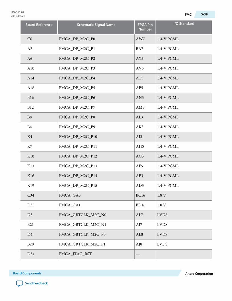
Board Reference Schematic Signal Name FPGA PinNumber
I/O Standard
C6 FMCA_DP_M2C_P0 AW7 1.4-V PCML
A2 FMCA_DP_M2C_P1 BA7 1.4-V PCML
A6 FMCA_DP_M2C_P2 AY5 1.4-V PCML
A10 FMCA_DP_M2C_P3 AV5 1.4-V PCML
A14 FMCA_DP_M2C_P4 AT5 1.4-V PCML
A18 FMCA_DP_M2C_P5 AP5 1.4-V PCML
B16 FMCA_DP_M2C_P6 AN3 1.4-V PCML
B12 FMCA_DP_M2C_P7 AM5 1.4-V PCML
B8 FMCA_DP_M2C_P8 AL3 1.4-V PCML
B4 FMCA_DP_M2C_P9 AK5 1.4-V PCML
K4 FMCA_DP_M2C_P10 AJ3 1.4-V PCML
K7 FMCA_DP_M2C_P11 AH5 1.4-V PCML
K10 FMCA_DP_M2C_P12 AG3 1.4-V PCML
K13 FMCA_DP_M2C_P13 AF5 1.4-V PCML
K16 FMCA_DP_M2C_P14 AE3 1.4-V PCML
K19 FMCA_DP_M2C_P15 AD5 1.4-V PCML
C34 FMCA_GA0 BC16 1.8 V
D35 FMCA_GA1 BD16 1.8 V
D5 FMCA_GBTCLK_M2C_N0 AL7 LVDS
B21 FMCA_GBTCLK_M2C_N1 AJ7 LVDS
D4 FMCA_GBTCLK_M2C_P0 AL8 LVDS
B20 FMCA_GBTCLK_M2C_P1 AJ8 LVDS
D34 FMCA_JTAG_RST —
UG-011702015.06.26 FMC 5-39
Board Components Altera Corporation
Send Feedback
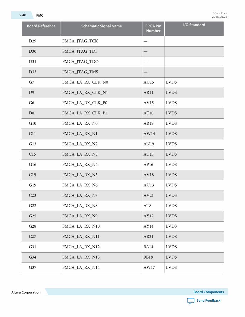
Board Reference Schematic Signal Name FPGA PinNumber
I/O Standard
D29 FMCA_JTAG_TCK —
D30 FMCA_JTAG_TDI —
D31 FMCA_JTAG_TDO —
D33 FMCA_JTAG_TMS —
G7 FMCA_LA_RX_CLK_N0 AU15 LVDS
D9 FMCA_LA_RX_CLK_N1 AR11 LVDS
G6 FMCA_LA_RX_CLK_P0 AV15 LVDS
D8 FMCA_LA_RX_CLK_P1 AT10 LVDS
G10 FMCA_LA_RX_N0 AR19 LVDS
C11 FMCA_LA_RX_N1 AW14 LVDS
G13 FMCA_LA_RX_N2 AN19 LVDS
C15 FMCA_LA_RX_N3 AT15 LVDS
G16 FMCA_LA_RX_N4 AP16 LVDS
C19 FMCA_LA_RX_N5 AV18 LVDS
G19 FMCA_LA_RX_N6 AU13 LVDS
C23 FMCA_LA_RX_N7 AV21 LVDS
G22 FMCA_LA_RX_N8 AT8 LVDS
G25 FMCA_LA_RX_N9 AY12 LVDS
G28 FMCA_LA_RX_N10 AY14 LVDS
C27 FMCA_LA_RX_N11 AR21 LVDS
G31 FMCA_LA_RX_N12 BA14 LVDS
G34 FMCA_LA_RX_N13 BB18 LVDS
G37 FMCA_LA_RX_N14 AW17 LVDS
5-40 FMCUG-01170
2015.06.26
Altera Corporation Board Components
Send Feedback
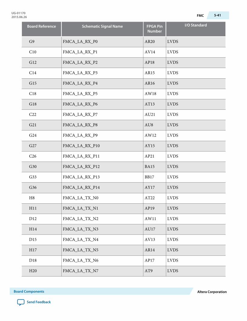
Board Reference Schematic Signal Name FPGA PinNumber
I/O Standard
G9 FMCA_LA_RX_P0 AR20 LVDS
C10 FMCA_LA_RX_P1 AV14 LVDS
G12 FMCA_LA_RX_P2 AP18 LVDS
C14 FMCA_LA_RX_P3 AR15 LVDS
G15 FMCA_LA_RX_P4 AR16 LVDS
C18 FMCA_LA_RX_P5 AW18 LVDS
G18 FMCA_LA_RX_P6 AT13 LVDS
C22 FMCA_LA_RX_P7 AU21 LVDS
G21 FMCA_LA_RX_P8 AU8 LVDS
G24 FMCA_LA_RX_P9 AW12 LVDS
G27 FMCA_LA_RX_P10 AY15 LVDS
C26 FMCA_LA_RX_P11 AP21 LVDS
G30 FMCA_LA_RX_P12 BA15 LVDS
G33 FMCA_LA_RX_P13 BB17 LVDS
G36 FMCA_LA_RX_P14 AY17 LVDS
H8 FMCA_LA_TX_N0 AT22 LVDS
H11 FMCA_LA_TX_N1 AP19 LVDS
D12 FMCA_LA_TX_N2 AW11 LVDS
H14 FMCA_LA_TX_N3 AU17 LVDS
D15 FMCA_LA_TX_N4 AV13 LVDS
H17 FMCA_LA_TX_N5 AR14 LVDS
D18 FMCA_LA_TX_N6 AP17 LVDS
H20 FMCA_LA_TX_N7 AT9 LVDS
UG-011702015.06.26 FMC 5-41
Board Components Altera Corporation
Send Feedback
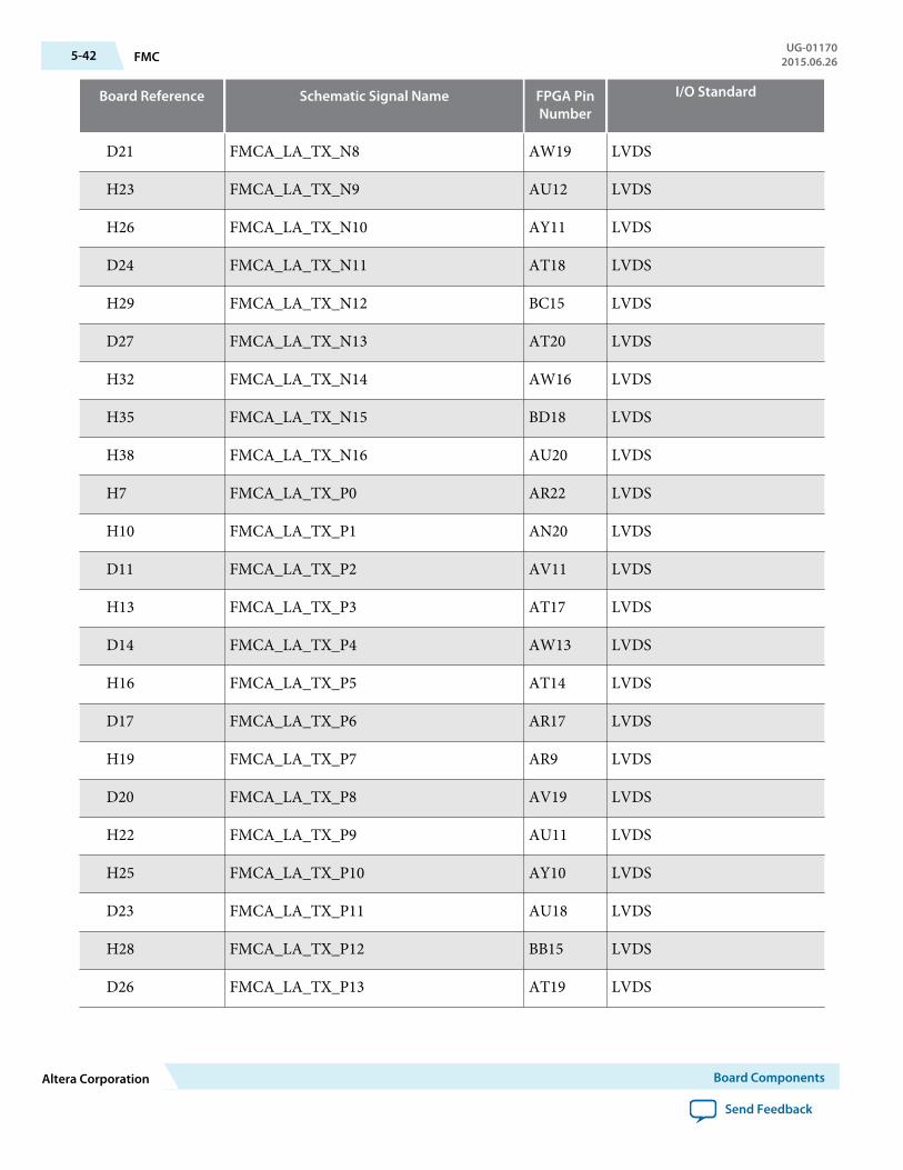
Board Reference Schematic Signal Name FPGA PinNumber
I/O Standard
D21 FMCA_LA_TX_N8 AW19 LVDS
H23 FMCA_LA_TX_N9 AU12 LVDS
H26 FMCA_LA_TX_N10 AY11 LVDS
D24 FMCA_LA_TX_N11 AT18 LVDS
H29 FMCA_LA_TX_N12 BC15 LVDS
D27 FMCA_LA_TX_N13 AT20 LVDS
H32 FMCA_LA_TX_N14 AW16 LVDS
H35 FMCA_LA_TX_N15 BD18 LVDS
H38 FMCA_LA_TX_N16 AU20 LVDS
H7 FMCA_LA_TX_P0 AR22 LVDS
H10 FMCA_LA_TX_P1 AN20 LVDS
D11 FMCA_LA_TX_P2 AV11 LVDS
H13 FMCA_LA_TX_P3 AT17 LVDS
D14 FMCA_LA_TX_P4 AW13 LVDS
H16 FMCA_LA_TX_P5 AT14 LVDS
D17 FMCA_LA_TX_P6 AR17 LVDS
H19 FMCA_LA_TX_P7 AR9 LVDS
D20 FMCA_LA_TX_P8 AV19 LVDS
H22 FMCA_LA_TX_P9 AU11 LVDS
H25 FMCA_LA_TX_P10 AY10 LVDS
D23 FMCA_LA_TX_P11 AU18 LVDS
H28 FMCA_LA_TX_P12 BB15 LVDS
D26 FMCA_LA_TX_P13 AT19 LVDS
5-42 FMCUG-01170
2015.06.26
Altera Corporation Board Components
Send Feedback

Board Reference Schematic Signal Name FPGA PinNumber
I/O Standard
H31 FMCA_LA_TX_P14 AY16 LVDS
H34 FMCA_LA_TX_P15 BC18 LVDS
H37 FMCA_LA_TX_P16 AV20 LVDS
F1 FMCA_M2C_PG —
H2 FMCA_PRSNTN P16 1.8 V
C30 FMCA_SCL AU10 1.8 V
C31 FMCA_SDA AV10 1.8 V
J39 VIO_B_M2C — —
K40 VIO_B_M2C — —
K1 VREF_B_M2C — —
H1 VREF_FMCA — —
Note: The FMC port B has the same pin assignments as port A but on a different board referencedesignation. For example, the pin assignments for FMCA_LA_TX_P1 is J1.H10 andFMCB_LA_TX_P1 is J2.H10.
QSFPThe Arria 10 GX FPGA development board includes a QSFP module.
Table 5-20: QSFP Pin Assignments, Schematic Signal Names, and Functions
Board Reference Schematic SignalName
FPGA PinNumber
I/O Standard Description
28 QSFP_3P3V_INTERRUPTN
AL34 1.8 V QSFP interrupt
31 QSFP_3P3V_LP_MODE
AK34 1.8 V QSFP low power mode
27 QSFP_3P3V_MOD_PRSN
AU36 1.8 V Module present
8 QSFP_3P3V_MOD_SELN
AU35 1.8 V Module select
UG-011702015.06.26 QSFP 5-43
Board Components Altera Corporation
Send Feedback
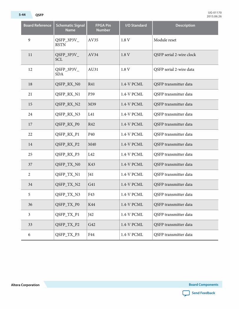
Board Reference Schematic SignalName
FPGA PinNumber
I/O Standard Description
9 QSFP_3P3V_RSTN
AV35 1.8 V Module reset
11 QSFP_3P3V_SCL
AV34 1.8 V QSFP serial 2-wire clock
12 QSFP_3P3V_SDA
AU31 1.8 V QSFP serial 2-wire data
18 QSFP_RX_N0 R41 1.4-V PCML QSFP transmitter data
21 QSFP_RX_N1 P39 1.4-V PCML QSFP transmitter data
15 QSFP_RX_N2 M39 1.4-V PCML QSFP transmitter data
24 QSFP_RX_N3 L41 1.4-V PCML QSFP transmitter data
17 QSFP_RX_P0 R42 1.4-V PCML QSFP transmitter data
22 QSFP_RX_P1 P40 1.4-V PCML QSFP transmitter data
14 QSFP_RX_P2 M40 1.4-V PCML QSFP transmitter data
25 QSFP_RX_P3 L42 1.4-V PCML QSFP transmitter data
37 QSFP_TX_N0 K43 1.4-V PCML QSFP transmitter data
2 QSFP_TX_N1 J41 1.4-V PCML QSFP transmitter data
34 QSFP_TX_N2 G41 1.4-V PCML QSFP transmitter data
5 QSFP_TX_N3 F43 1.4-V PCML QSFP transmitter data
36 QSFP_TX_P0 K44 1.4-V PCML QSFP transmitter data
3 QSFP_TX_P1 J42 1.4-V PCML QSFP transmitter data
33 QSFP_TX_P2 G42 1.4-V PCML QSFP transmitter data
6 QSFP_TX_P3 F44 1.4-V PCML QSFP transmitter data
5-44 QSFPUG-01170
2015.06.26
Altera Corporation Board Components
Send Feedback

SFP+The Arria 10 GX FPGA development board includes one SFP+ module that uses transceiver channelsfrom the FPGA. This module takes in serial data from the FPGA and transform them into optical signals.The Arria 10 GX FPGA development board includes one SFP+ cage assembly for the SFP+ port that isused by the device.
Table 5-21: SFP+ Pin Assignments, Schematic Signal Names, and Functions
BoardReference (J12)
Schematic Signal Name FPGA PinNumber
I/O Standard Description
6 SFP_3P3V_MOD0_PRSNTN
AT30 1.8 V Module present indicator
7 SFP_3P3V_RS0 AN31 1.8 V SFP+ rate select 0
9 SFP_3P3V_RS1 AT34 1.8 V SFP+ rate select 1
8 SFP_3P3V_RX_LOS AU30 1.8 V Signal present indicator
3 SFP_3P3V_TX_DIS AR35 1.8 V Transmitter disable
2 SFP_3P3V_TX_FLT AT35 1.8 V Transmitter fault
12 SFP_RX_N AA41 1.4-V PCML Receiver data
13 SFP_RX_P AA42 1.4-V PCML Receiver data
5 SFP_SCL — 1.8 V Serial 2-wire clock
4 SFP_SDA — 1.8 V Serial 2-wire data
19 SFP_TX_N AB43 1.4-V PCML Transmitter data
18 SFP_TX_P AB44 1.4-V PCML Transmitter data
I2CI2C supports communication between integrated circuits on a board. It is a simple two-wire bus thatconsists of a serial data line (SDA) and a serial clock (SCL). The MAX V and Arria 10 devices use the I2Cfor reading and writing to the character LCD. You can use the Arria 10 or MAX V as the I2C host toaccess the PLLs and clocks.
UG-011702015.06.26 SFP+ 5-45
Board Components Altera Corporation
Send Feedback
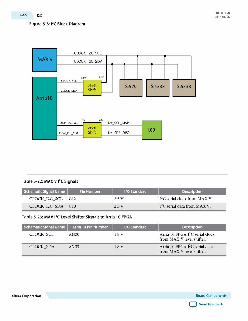
Figure 5-3: I2C Block Diagram
MAX V
Arria10
LCDi2c_SCL_DISP
i2c_SDA_DISP
CLOCK_I2C_SDA
CLOCK_I2C_SCL
Level Shift
Level Shift
CLOCK_SCL
CLOCK_SDA
DISP_I2C_SCL
DISP_I2C_SDA
Si570 Si5338 Si5338
1.8V
1.8V 5.0V
2.5V
Table 5-22: MAX V I2C Signals
Schematic Signal Name Pin Number I/O Standard Description
CLOCK_I2C_SCL C12 2.5 V I2C serial clock from MAX V.CLOCK_I2C_SDA C10 2.5 V I2C serial data from MAX V.
Table 5-23: MAV I2C Level Shifter Signals to Arria 10 FPGA
Schematic Signal Name Arria 10 Pin Number I/O Standard Description
CLOCK_SCL AN30 1.8 V Arria 10 FPGA I2C serial clockfrom MAX V level shifter.
CLOCK_SDA AV33 1.8 V Arria 10 FPGA I2C serial datafrom MAX V level shifter.
5-46 I2CUG-01170
2015.06.26
Altera Corporation Board Components
Send Feedback

Table 5-24: Arria 10 I2C Signals
Schematic Signal Name Pin Number I/O Standard Description
DISP_I2C_SCL AW33 1.8 V Arria 10 I2C serial clock to levelshifter.
DISP_I2C_SDA AY34 1.8 V Arria 10 I2C serial data to levelshifter.
Table 5-25: Arria 10 I2C Level Shifter to LCD Signals
Schematic Signal Name LCD Pin Number I/O Standard Description
I2C_SCL_DISP 7 5.0 V LCD I2C serial clock from Arria10 FPGA level shifter.
I2C_SDA_DISP 8 5.0 V LCD I2C serial data from Arria10 FPGA level shifter.
UG-011702015.06.26 I2C 5-47
Board Components Altera Corporation
Send Feedback
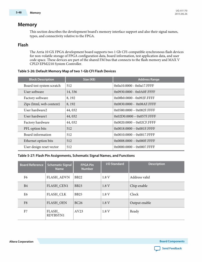
MemoryThis section describes the development board's memory interface support and also their signal names,types, and connectivity relative to the FPGA.
FlashThe Arria 10 GX FPGA development board supports two 1 Gb CFI-compatible synchronous flash devicesfor non-volatile storage of FPGA configuration data, board information, test application data, and usercode space. These devices are part of the shared FM bus that connects to the flash memory and MAX VCPLD EPM2210 System Controller.
Table 5-26: Default Memory Map of two 1-Gb CFI Flash Devices
Block Description Size (KB) Address Range
Board test system scratch 512 0x0a10.0000 - 0x0a17.FFFFUser software 14, 336 0x0930.0000 - 0x0A0F.FFFFFactory software 8, 192 0x08b0.0000 - 0x092F.FFFFZips (html, web content) 8, 192 0x0830.0000 - 0x08AF.FFFFUser hardware2 44, 032 0x0580.0000 – 0x082F.FFFFUser hardware1 44, 032 0x02D0.0000 – 0x057F.FFFFFactory hardware 44, 032 0x0020.0000 – 0x02CF.FFFFPFL option bits 512 0x0018.0000 – 0x001F.FFFFBoard information 512 0x0010.0000 – 0x0017.FFFFEthernet option bits 512 0x0008.0000 – 0x000F.FFFFUser design reset vector 512 0x0000.0000 – 0x0007.FFFF
Table 5-27: Flash Pin Assignments, Schematic Signal Names, and Functions
Board Reference Schematic SignalName
FPGA PinNumber
I/O Standard Description
F6 FLASH_ADVN BB22 1.8 V Address valid
B4 FLASH_CEN1 BB23 1.8 V Chip enable
E6 FLASH_CLK BB25 1.8 V Clock
F8 FLASH_OEN BC26 1.8 V Output enable
F7 FLASH_RDYBSYN1
AV23 1.8 V Ready
5-48 MemoryUG-01170
2015.06.26
Altera Corporation Board Components
Send Feedback

Board Reference Schematic SignalName
FPGA PinNumber
I/O Standard Description
D4 FLASH_RESETN
BA23 1.8 V Reset
G8 FLASH_WEN BD26 1.8 V Write enable
C6 FLASH_WPN — 1.8 V Write protect
A1 FM_A1 AM11 1.8 V Address bus
B1 FM_A2 AM12 1.8 V Address bus
C1 FM_A3 AL12 1.8 V Address bus
D1 FM_A4 AN13 1.8 V Address bus
D2 FM_A5 AM13 1.8 V Address bus
A2 FM_A6 AE12 1.8 V Address bus
C2 FM_A7 AN15 1.8 V Address bus
A3 FM_A8 AL10 1.8 V Address bus
B3 FM_A9 AR10 1.8 V Address bus
C3 FM_A10 AP11 1.8 V Address bus
D3 FM_A11 AL13 1.8 V Address bus
C4 FM_A12 AH11 1.8 V Address bus
A5 FM_A13 AN14 1.8 V Address bus
B5 FM_A14 AG11 1.8 V Address bus
C5 FM_A15 AH10 1.8 V Address bus
D7 FM_A16 AF14 1.8 V Address bus
D8 FM_A17 AF15 1.8 V Address bus
A7 FM_A18 AH14 1.8 V Address bus
B7 FM_A19 AJ12 1.8 V Address bus
C7 FM_A20 AJ14 1.8 V Address bus
UG-011702015.06.26 Flash 5-49
Board Components Altera Corporation
Send Feedback
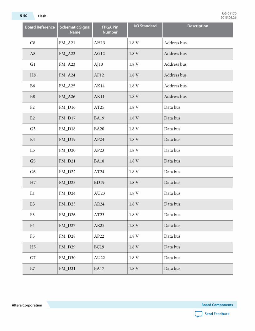
Board Reference Schematic SignalName
FPGA PinNumber
I/O Standard Description
C8 FM_A21 AH13 1.8 V Address bus
A8 FM_A22 AG12 1.8 V Address bus
G1 FM_A23 AJ13 1.8 V Address bus
H8 FM_A24 AF12 1.8 V Address bus
B6 FM_A25 AK14 1.8 V Address bus
B8 FM_A26 AK11 1.8 V Address bus
F2 FM_D16 AT25 1.8 V Data bus
E2 FM_D17 BA19 1.8 V Data bus
G3 FM_D18 BA20 1.8 V Data bus
E4 FM_D19 AP24 1.8 V Data bus
E5 FM_D20 AP23 1.8 V Data bus
G5 FM_D21 BA18 1.8 V Data bus
G6 FM_D22 AT24 1.8 V Data bus
H7 FM_D23 BD19 1.8 V Data bus
E1 FM_D24 AU23 1.8 V Data bus
E3 FM_D25 AR24 1.8 V Data bus
F3 FM_D26 AT23 1.8 V Data bus
F4 FM_D27 AR25 1.8 V Data bus
F5 FM_D28 AP22 1.8 V Data bus
H5 FM_D29 BC19 1.8 V Data bus
G7 FM_D30 AU22 1.8 V Data bus
E7 FM_D31 BA17 1.8 V Data bus
5-50 FlashUG-01170
2015.06.26
Altera Corporation Board Components
Send Feedback
Board Power SupplyThis section describes the Arria 10 GX FPGA development board’s power supply. A laptop style DCpower supply is provided with the development kit. Use only the supplied power supply. The powersupply has an auto sensing input voltage range of 100 ~ 240 VAC and will output 12 VDC power at 16 Ato the development board. The 12 VDC input power is then stepped down to various power rails used bythe board components.
An on-board multi-channel analog-to-digital converter (ADC) measures both the voltage and current forseveral specific board rails. The power utilization is displayed on a graphical user interface (GUI) that cangraph power consumption versus time.
Power Distribution SystemThe following figure below shows the power distribution system on the A10 FPGA development board.Regulator efficiencies and sharing are reflected in the currents shown, which are at conservative absolutemaximum levels.
UG-011702015.06.26 Board Power Supply 5-51
Board Components Altera Corporation
Send Feedback
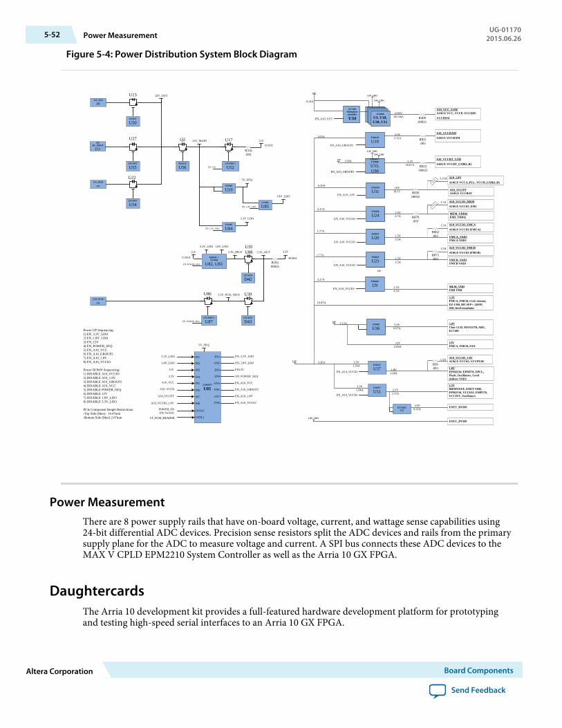
Figure 5-4: Power Distribution System Block Diagram
12V DC_INPUT
J13
LTC4357
U55
LTC4357
U54
ISL6115
U56
12V_MAIN
EN_12V
12V_PCIE
J22
LT4357
U50
12V_ATX
J4
12V_OUT
LTC4352
D43
3.3V_PCIE
J22
ED8101 +ET4040
U82, U83
LTC4352
D42
LTC4365-1
U52
12V
A10_VCC_LOWA10GX VCC, VCCP, VCCHIP,
VCCHSSI
A10_VCCRAM
A10GX VCCRAM
A10_VCCRT_GXB
A10GX VCCRT_GXB(L,R)
EC7401Multiphase controller
U34ET4040
U3, U18, U30, U11
EN63A0
U10
ED8101 + ET4040
U33, U90
EN63A0
U31
EN6360
U24
EN6347
U20
EN6347
U23
EN6360
U9
1.1V16.67A
1.8V10.23
1.5V4.7A
0.95V105.06A
12V
12V
0.955.12A
A10_1.8V
A10GX VCCA_PLL, VCCH_GXB(L,R)
A10_VCCPTA10GX VCCBAT
BEAD3.13A
A10_VCCIO_MEM
A10GX VCCIO_EMI
MEM_VDDQEMI_VDDQ
BEAD1.5A
1.5V3.5A
A10_VCCIO_FMCA
A10GX VCCIO (FMCA)
FMCA_VADJFMCA VADJ
1.5A
1.5V3.5A
A10_VCCIO_FMCB
A10GX VCCIO (FMCB)
FMCB_VADJFMCB VADJ
1.5A
1.5V4.5A
MEM_VDDEMI VDD
3.3VFMCA, FMCB, CLK cleaner, EZ-USB, DP, SFP+, QSFP, SDI, level translator
10.87A
LT3082
U365.0VChar LCD, MAX3378, ADC, EC7401
5.0V0.07A
12VFMCA, FMCB, FAN
EN6337
U57
A10_VCCIO_1.8VA10GX VCCIO, VCCPGM
EN6337
U51 2.5V2.31A
1.8VEPM2210, EPM570, EPCL, Flash, Oscillators, Level shifters VADJ
2.5VMEMVEXT, ENET VDD, EPM2210, VCCIO1, EMP570, VCCINT, Oscillators
1.5A
1.8V2.08A
3.3V1.26A
3.3V1.94A
LTC3025U25
ENET_DVDD1.0V0.21A
EN_POWER_SEQ
3.3V_LDO
LT1965
U84
3.3V_MUX 3.3V
3.3V_LDO 1.8V_LDO
R408.00025
R811.003
R823.00025
R850.00025
R879.003
R862.003
R871.003
R95.003
12V
3.3V
3.3V_LDO
1.8V_LDO
ENET_DVDD1.8V_LDO
EN_POWER_SEQ
LTC4365-1
U87
EN_3.3V_LDO
LT1965
U19
5V_SEQ
LTM2977
U81
5V_SEQ
EN1
EN2
EN3
EN4
EN5
EN6
EN7
EN8
EN_3.3V_LDO
EN_1.8V_LDO
EN_POWER_SEQ
CNTL0
CNTL1
POWER_EN(On Switch)
LT_PGM_HEADER
EN_A10_VCC
EN_A10_GROUP2
EN_A10_1.8V
EN_A10_VCCIO
EN_A10_VCC
EN_A10_GROUP2
EN_A10_GROUP2
EN_A10_1.8V
EN_A10_VCCIO
EN_A10_VCCIO
EN_A10_VCCIO
EN_A10_VCCIO
EN_A10_VCCIO
EN_A10_VCCIO
12V
EN12V
Power UP Sequencing:1) EN_3.3V_LDO2) EN_1.8V_LDO3) EN_12V4) EN_POWER_SEQ5) EN_A10_VCC6) EN_A10_GROUP27) EN_A10_1.8V8) EN_A10_VCCIO
Power DOWN Sequencing:1) DISABLE A10_VCCIO2) DISABLE A10_1.8V3) DISABLE A10_GROUP24) DISABLE A10_VCC5) DISABLE POWER_SEQ6) DISABLE 12V7) DISABLE 1.8V_LDO8) DISABLE 3.3V_LDO
PCIe Component Height Restrictions:-Top Side (Max): 14.47mm-Bottom Side (Max) 2.67mm
3.3V_LDO
1.8V_LDO
12V
3.3V
A10_VCC
A10_VCCR
A10_VCCPT
A10_VCCIO_1.8V
IN1
IN2
IN3
IN4
IN5
IN6
IN7
IN8
U13
U27
U22
Q2 U17
U35 U88
U39
12V2.09A
U86 3.3V_PCIE_MUX
1.63A
1.69A
6.20A
2.37A
1.77A
1.77A
2.27A
3.20A
30.08A
9.24A
11.05A
12V
3.3V_LDO
1.8V_LDO
2.12A
13.05A
R316.003
R165.00025
3.3V_OUT
1.8V_LDO
LT1965
U85EN_1.8V_LDO
Power MeasurementThere are 8 power supply rails that have on-board voltage, current, and wattage sense capabilities using24-bit differential ADC devices. Precision sense resistors split the ADC devices and rails from the primarysupply plane for the ADC to measure voltage and current. A SPI bus connects these ADC devices to theMAX V CPLD EPM2210 System Controller as well as the Arria 10 GX FPGA.
DaughtercardsThe Arria 10 development kit provides a full-featured hardware development platform for prototypingand testing high-speed serial interfaces to an Arria 10 GX FPGA.
5-52 Power MeasurementUG-01170
2015.06.26
Altera Corporation Board Components
Send Feedback
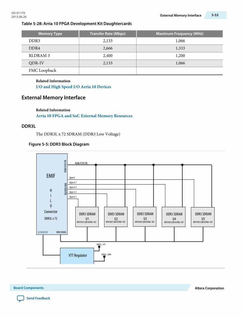
Table 5-28: Arria 10 FPGA Development Kit Daughtercards
Memory Type Transfer Rate (Mbps) Maximum Frequency (MHz)
DDR3 2,133 1,066DDR4 2,666 1,333RLDRAM 3 2,400 1,200QDR-IV 2,133 1,066FMC Loopback
Related InformationI/O and High Speed I/O Arria 10 Devices
External Memory Interface
Related InformationArria 10 FPGA and SoC External Memory Resources
DDR3L
The DDR3L x 72 SDRAM (DDR3 Low Voltage)
Figure 5-5: DDR3 Block Diagram
VDD/VDDQ
EMIF
HILO
Connector
DDR3L x 72DDR3 SDRAM
U1DDR3 SDRAM
U2DDR3 SDRAM
U3DDR3 SDRAM
U4DDR3 SDRAM
U5
Byte 8
Byte 6-7
Byte 4-5
Byte 2-3
Byte 0-1
DQ/D
QS/D
MAd
dr/C
trl/cl
k
Addr/Ctrl/clk
3.3 V/2.5 V
VTT Regulator
DDR3L_VTT
DDR3L_VREF
MT41K512M16TNA-107 MT41K512M16TNA-107 MT41K512M16TNA-107 MT41K512M16TNA-107 MT41K512M16TNA-107
UG-011702015.06.26 External Memory Interface 5-53
Board Components Altera Corporation
Send Feedback

DDR4
DDR4 x 72 SDRAM
Figure 5-6: DDR4 Block Diagram
VDD/2.5 V
EMIF
HILO
Connector
DDR4 x 72DDR4 SDRAM
U1DDR4 SDRAM
U2DDR4 SDRAM
U3DDR4 SDRAM
U4DDR4 SDRAM
U5
Byte 8
Byte 6-7
Byte 4-5
Byte 2-3
Byte 0-1
DQ/D
QS/D
MAd
dr/C
trl/cl
k
RLDRAM 3
The RLDRAM 3 x 36 (reduced latency DRAM) controller is designed for use in applications requringhigh memory throughput, high clock rates and full programmablity.
5-54 DDR4UG-01170
2015.06.26
Altera Corporation Board Components
Send Feedback
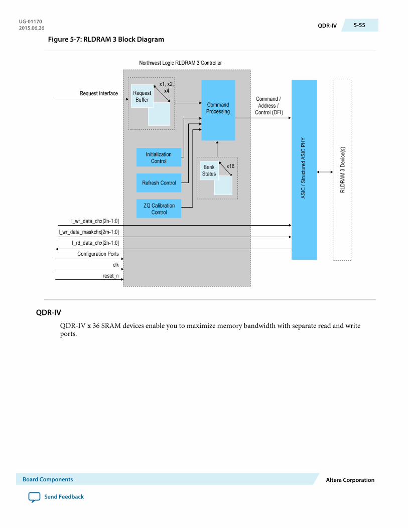
Figure 5-7: RLDRAM 3 Block Diagram
QDR-IV
QDR-IV x 36 SRAM devices enable you to maximize memory bandwidth with separate read and writeports.
UG-011702015.06.26 QDR-IV 5-55
Board Components Altera Corporation
Send Feedback
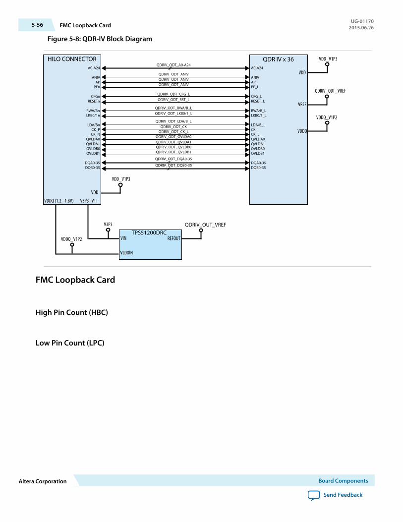
Figure 5-8: QDR-IV Block Diagram
V3P3_VTTVDDQ (1.2 - 1.8V)
VDD
VLDOIN
VIN
V3P3
VDD_V1P3
VDDQ_V1P2 REFOUTTPS51200DRC
QDRIV_OUT_VREF
HILO CONNECTORA0-A24
ANIVAP
PEn
CFGnRESETn
RWA/BnLKB0/1n
LDA/BnCK_PCK_N
QVLDA0QVLDA1QVLDB0QVLDB1
DQA0-35DQB0-35
A0-A24
ANIVAPPE_L
CFG_LRESET_L
RWA/B_LLKB0/1_L
LDA/B_LCKCK_LQVLDA0QVLDA1QVLDB0QVLDB1
DQA0-35DQB0-35
QDR IV x 36
VDD
VREF
VDDQ
VDD_V1P3
QDRIV_ODT_VREF
VDDQ_V1P2
QDRIV_ODT_A0-A24
QDRIV_ODT_DQA0-35
QDRIV_ODT_DQB0-35
QDRIV_ODT_ANIV
QDRIV_ODT_CFG_LQDRIV_ODT_RST_L
QDRIV_ODT_RWA/B_LQDRIV_ODT_LKB0/1_L
QDRIV_ODT_LDA/B_LQDRIV_ODT_CK
QDRIV_ODT_CK_LQDRIV_ODT_QVLDA0QDRIV_ODT_QVLDA1QDRIV_ODT_QVLDB0QDRIV_ODT_QVLDB1
QDRIV_ODT_ANIVQDRIV_ODT_ANIV
FMC Loopback Card
High Pin Count (HBC)
Low Pin Count (LPC)
5-56 FMC Loopback CardUG-01170
2015.06.26
Altera Corporation Board Components
Send Feedback

Additional Information A2015.06.26
UG-01170 Subscribe Send Feedback
Board & User Guide Revision History
Table A-1: Arria 10 FPGA Development Kit User Guide Revision History
Date Version Changes
June 2015 2015.06.26 Initial release.
Compliance and Conformity Statements
CE EMI Conformity CautionThis board is delivered conforming to relevant standards mandated by Directive 2004/108/EC. Because ofthe nature of programmable logic devices, it is possible for the user to modify the kit in such a way as togenerate electromagnetic interference (EMI) that exceeds the limits established for this equipment. AnyEMI caused as the result of modifications to the delivered material is the responsibility of the user.
© 2015 Altera Corporation. All rights reserved. ALTERA, ARRIA, CYCLONE, ENPIRION, MAX, MEGACORE, NIOS, QUARTUS and STRATIX words and logos aretrademarks of Altera Corporation and registered in the U.S. Patent and Trademark Office and in other countries. All other words and logos identified astrademarks or service marks are the property of their respective holders as described at www.altera.com/common/legal.html. Altera warrants performanceof its semiconductor products to current specifications in accordance with Altera's standard warranty, but reserves the right to make changes to anyproducts and services at any time without notice. Altera assumes no responsibility or liability arising out of the application or use of any information,product, or service described herein except as expressly agreed to in writing by Altera. Altera customers are advised to obtain the latest version of devicespecifications before relying on any published information and before placing orders for products or services.
ISO9001:2008Registered
www.altera.com101 Innovation Drive, San Jose, CA 95134


